tsek03 lab 1: lna simulation using cadence spectrerf · 1.2 cadence and pdk setup guidelines 1....
TRANSCRIPT
TSEK03 Integrated Radio Frequency Circuits 2018/Ted Johansson 1/26
TSEK03 LAB 1:
LNA simulation using Cadence SpectreRF
Ver. 2018-09-18 for Cadence 6 & MMSIM 14
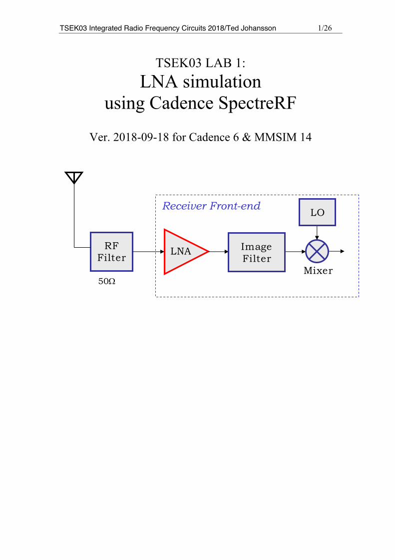
RF Filter LNA Image
Filter
Receiver Front-end
50W
LO
Mixer
TSEK03 Integrated Radio Frequency Circuits 2018/Ted Johansson 2/26
1. Introduction This lab describes how to use Cadence SpectreRF in Analog Design Environment to simulate parameters that are important in design and verification of Low Noise Amplifiers (LNAs). The lab is based on a Cadence SpectreRF Workshop session and its manual "LNA Design Using SpectreRF" (previous called Application Note) which is found on the course page. To characterize the LNA, following figure of merits are usually measured or simulated:
1. Power Consumption and Supply Voltage 2. Gain 3. Noise 4. Input and Output Impedance Matching 5. Reverse Isolation 6. Stability 7. Linearity
We will use S-Parameters (SP), Harmonic Balance (hb), and hbnoise analysis available in SpectreRF to simulate the parameters listed above. Usually there is more than one method available to simulate the desired parameter in the Application Note. Some alternative simulation methods are discussed. Simulation lab overview:
1. S-Parameter Analysis (sp) • Small Signal Gain (S21, GA, GT, GP) • Small Signal Stability (Kf and ∆ or Bif ) • Small Signal Noise (SP and Pnoise) • Input and Output Matching (S11, S22, Z11, Z22)
2. Large Signal Noise Simulation (hb and hbnoise) 3. Gain Compression (Swept hb and Xdb) 4. IP3 Measurement: hb Analysis with Two Tones
1.1 Lab Instruction If the lab is not finished in the scheduled time slot, you can complete it in your own time. If there is any problem, send an email or show up in the office of the instructor. You must answer the questions in the lab manual’s section 2 before you start the lab, this will help you to comprehend the lab material and simulations methodology.
There are also a questions during the lab after some of the simulations that you must answer!

TSEK03 Integrated Radio Frequency Circuits 2018/Ted Johansson 3/26
1.2 Cadence and PDK Setup Guidelines 1. Please read the complete lab manual and the Cadence Workshop document
before you start the software. You will be using Cadence 6 (6.16 + MMSIM 14.1) and AMS 0.35 um CMOS (c35b4) process (PDK) in this lab.
• Open a terminal session and establish a ssh connection to the ixtab server through the command: ssh ixtab, then input your credentials.
• Remove any previously loaded Cadence modules (Type module on command prompt and read the instruction. This instruction will guide you how to list, load and remove the modules), or simply start a new terminal window.
• Create a new directory 'tsek03_lab1' where your simulation data will be stored: mkdir tsek03_lab1.
• cd tsek03_lab1, then do the rest of the steps from this directory. • Load the cadence files: module add cadence/6.16.090 • Load the AMS PDK files: module add ams/4.10 • Set variable IUSDIR to your library: setenv IUSDIR .
(please note the space and period (.) after IUSDIR) • Start cadence with the AMS PDK:
ams_cds -tech c35b4 -mode fb & • You must now choose a technology the first time you run this. In the
CIW window: HIT-KIT Utilities à Select Process Option and then choose C35B4C3 PIP VG5 HIRES.
2. When creating schematics, use the RF NMOS transistors from library PRIMLIBRF. The transistor models are valid up to 6 GHz. The models provided in PRIMLIB are only valid up to 1 GHz. The maximum allowable size of NMOS in SpectreRF is 200 um (20 fingers of 10 um or 40 fingers of 5 um). If you need larger transistors, use two transistors in parallel.
3. Use analogLib for other active and passive components. In Library Manager
click on Show Categories box on the top of window, this will show you the categories of components.
4. There are many views available when you place the symbol in schematic, use Symbol or Spectre view only.

TSEK03 Integrated Radio Frequency Circuits 2018/Ted Johansson 4/26
2. Background preparation Please read the Application Note “Spectre RF Workshop, LNA Design Using SpectreRF” (SpectreRF_LNA_MMSIM141.pdf), pp. 5-13, available on the course page, and together with the lecture material answer the following questions before you attend the lab. • Define Transducer Power Gain (GT), Operating Power Gain (GP), and Available
Power Gain (GA) for a two-port network.
• How can we relate the S-Parameters to the gain, input impedance and output impedance of any two-port network?
• Why is the reverse isolation gain important in the LNA design? Which S-parameter directly characterizes the reverse isolation gain?
• What is Stern stability factor? What is minimum condition of stability for an amplifier?

TSEK03 Integrated Radio Frequency Circuits 2018/Ted Johansson 5/26
3. LNA Simulation
3.1 Circuit Simulation Setup • Load cadence and PDK and start using instructions given in section 1.
Make a new library rf_lab1 in Cadence Library Manager and attach this library to the TECH_C35B4 technology file.
• Create and draw the schematic LNA as shown in Fig. 1. The components values are listed below.
• M1, M2 = 200 um/0.35 um, choose ”number of gates” to have larger width of transistors, Mbias = 60 um/0.35 um.
• Ls = 700 pH, Lg = 12 nH, Ld = 6 nH, Rd = 700 Ω.
Fig. 1. LNA Circuit Diagram (Source Inductor Degenerated LNA)
TSEK03 Integrated Radio Frequency Circuits 2018/Ted Johansson 6/26 • Once you have entered the schematic, make sure that can be saved without
errors. • Before you can place the LNA in a design hierarchy, you must create a
symbol. From the schematic window go to: Create à Cellview à From Cellview. You can either use the generic symbol or edit/draw a new one.
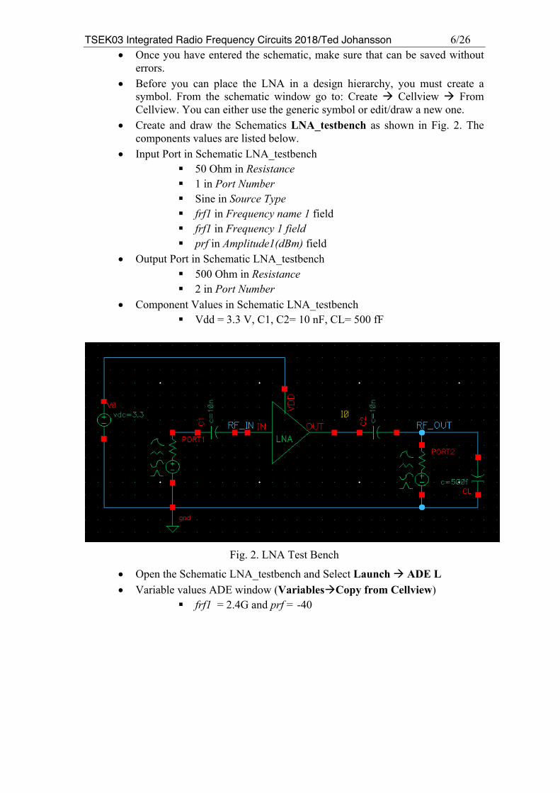
• Create and draw the Schematics LNA_testbench as shown in Fig. 2. The components values are listed below.
• Input Port in Schematic LNA_testbench § 50 Ohm in Resistance § 1 in Port Number § Sine in Source Type § frf1 in Frequency name 1 field § frf1 in Frequency 1 field § prf in Amplitude1(dBm) field
• Output Port in Schematic LNA_testbench § 500 Ohm in Resistance § 2 in Port Number
• Component Values in Schematic LNA_testbench § Vdd = 3.3 V, C1, C2= 10 nF, CL= 500 fF
Fig. 2. LNA Test Bench
• Open the Schematic LNA_testbench and Select Launch à ADE L • Variable values ADE window (VariablesàCopy from Cellview)
§ frf1 = 2.4G and prf = -40

TSEK03 Integrated Radio Frequency Circuits 2018/Ted Johansson 7/26
3.2 Small Signal Gain, NF, Impedance Matching and Stability using S-parameters
• In the ADE L window, select Analyses à Choose. The Choosing Analyses window shows:
§ Select sp for Analysis § In port field click on Select and then activate the schematic (if
not activated automatically), choose the input port first and then the output port. The names of two selected ports will appear in Ports field.
§ Sweep Variable: Frequency § Sweep Range (start-stop): 1G to 5G § Sweep Type: Automatic § Do Noise: Yes § Select Input and output ports accordingly by clicking Select
and then clicking at the appropriate Port in Schematic § Make sure that Enabled Box is checked then click OK.
• In the ADE L window click on Simulation à Netlist and Run to start the
simulation. Make sure that simulation completes without errors. Check the log in the CIW carefully! There may be an error, such as "ERROR (ADE-3036): Errors encountered during simulation". If so, try SetupàEnvironment. Set Run with 64 bit binary in the ADE L Window and run again.
• Now in the ADE L window click on the Resultsà Direct plotà Main Form
TSEK03 Integrated Radio Frequency Circuits 2018/Ted Johansson 8/26
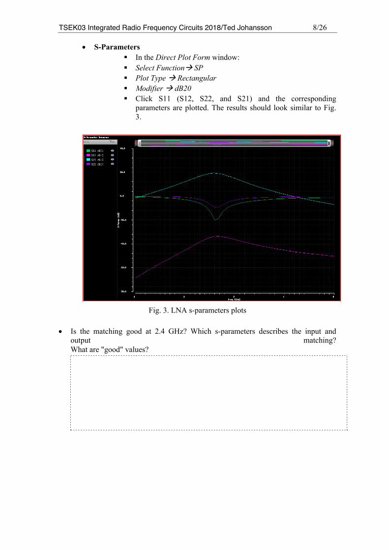
• S-Parameters § In the Direct Plot Form window: § Select Functionà SP § Plot Type à Rectangular § Modifier à dB20 § Click S11 (S12, S22, and S21) and the corresponding
parameters are plotted. The results should look similar to Fig. 3.
Fig. 3. LNA s-parameters plots
• Is the matching good at 2.4 GHz? Which s-parameters describes the input and output matching? What are "good" values?

TSEK03 Integrated Radio Frequency Circuits 2018/Ted Johansson 9/26 • GT, GA and GP (different type of Gains)
§ In the Direct Plot Form window: § Select Functionà GT, GA and GP (one by one) § Modifier à dB10 § Press the PLOT button; the result should be similar to Fig. 4.
Fig 4. GT, GA, and GP The power gain GP is closer to the transducer gain GT than the available gain GA, which means that the input matching network is properly designed, i.e. s11 is close to zero.
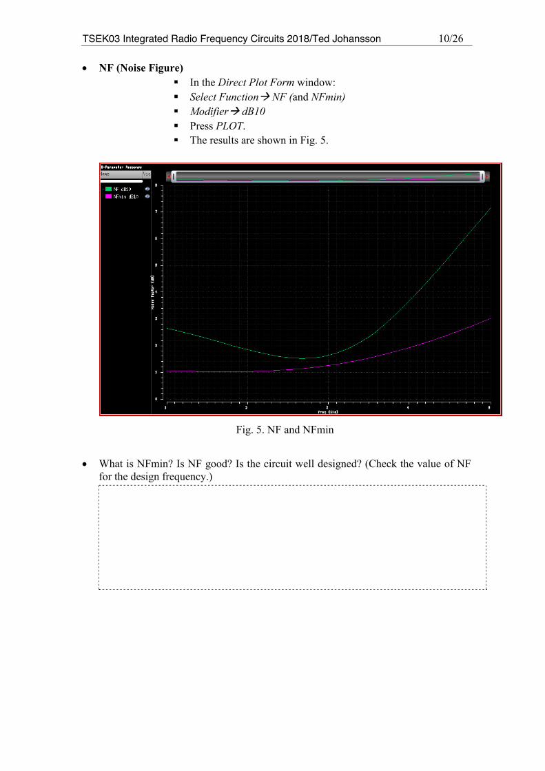
TSEK03 Integrated Radio Frequency Circuits 2018/Ted Johansson 10/26 • NF (Noise Figure)
§ In the Direct Plot Form window: § Select Functionà NF (and NFmin) § Modifierà dB10 § Press PLOT. § The results are shown in Fig. 5.
Fig. 5. NF and NFmin
• What is NFmin? Is NF good? Is the circuit well designed? (Check the value of NF
for the design frequency.)
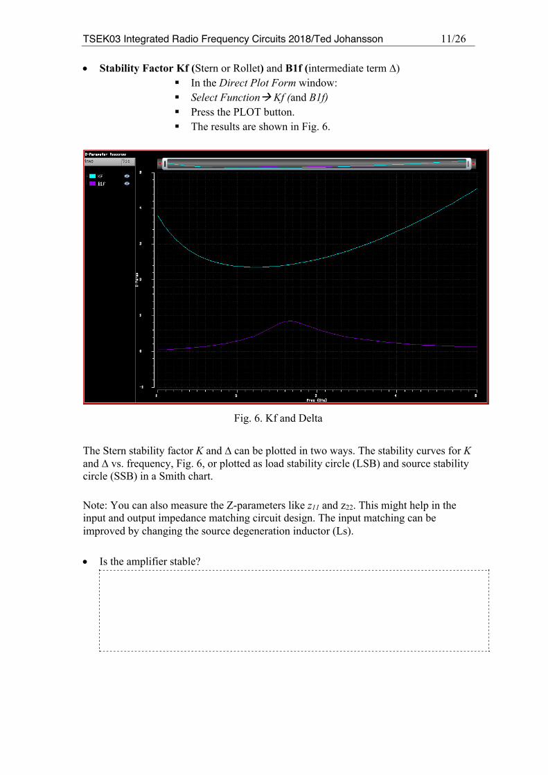
TSEK03 Integrated Radio Frequency Circuits 2018/Ted Johansson 11/26 • Stability Factor Kf (Stern or Rollet) and B1f (intermediate term ∆)
§ In the Direct Plot Form window: § Select Functionà Kf (and B1f) § Press the PLOT button. § The results are shown in Fig. 6.
Fig. 6. Kf and Delta
The Stern stability factor K and ∆ can be plotted in two ways. The stability curves for K and ∆ vs. frequency, Fig. 6, or plotted as load stability circle (LSB) and source stability circle (SSB) in a Smith chart.
Note: You can also measure the Z-parameters like z11 and z22. This might help in the input and output impedance matching circuit design. The input matching can be improved by changing the source degeneration inductor (Ls).
• Is the amplifier stable?

TSEK03 Integrated Radio Frequency Circuits 2018/Ted Johansson 12/26
3.3 NF by Large Signal Noise Simulation (hb and hbnoise Analysis) Use the hb and hbnoise analyses for large-signal and nonlinear noise analyses, where the circuits are linearized around the periodic steady-state operating point (the Noise and SP analyses are used for small-signal and linear noise analyses, where the circuits are linearized around the DC operating point.) As the input power level increases, the circuit becomes nonlinear, harmonics are generated, and the noise spectrum is folded. Therefore, you should use the hb and hbnoise analyses. When the input power level remains low, the NF calculated from the hbnoise, hbsp, Noise, and SP analyses should all match.
• Verify the variable values in the ADE L window
§ frf1 = 2.4 GHz § pr1f = -20
• In the ADE L window, select Analysesà Choose • The Choose Analyses window shows
§ Select hb for Analysis § See Fig. 7 for parameter settings § Make sure that Enabled Box is checked then click OK.
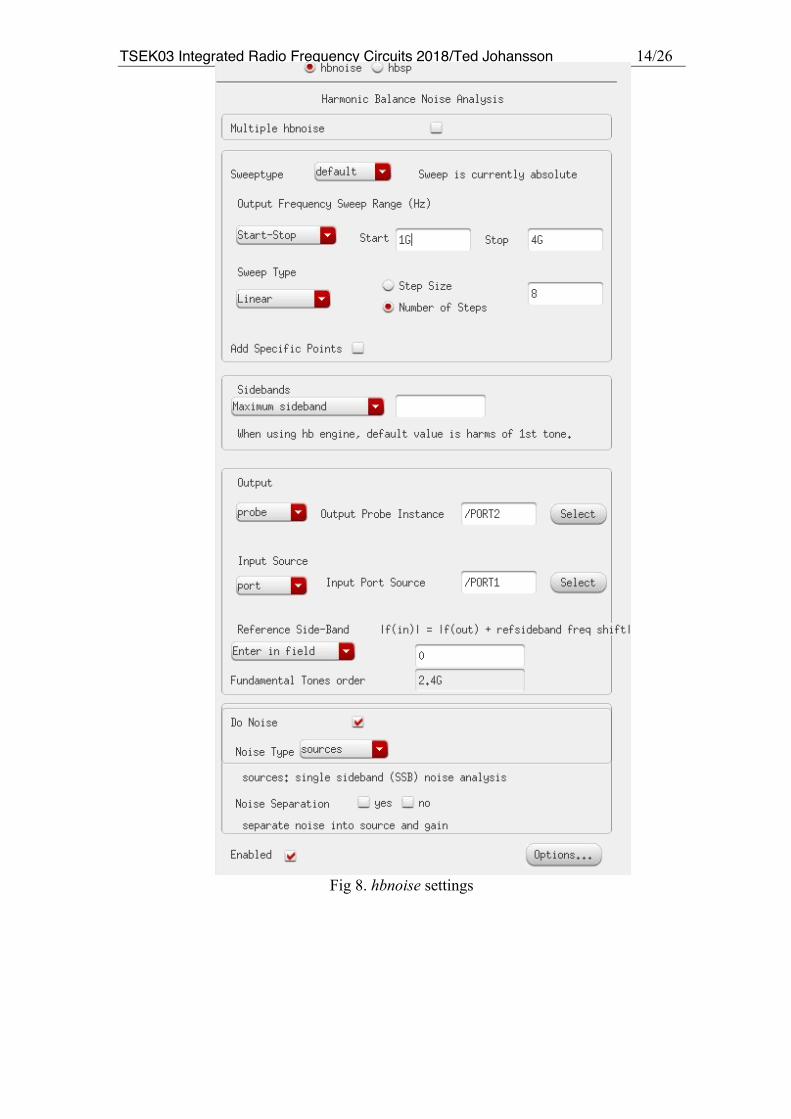
• And again, select Analysesà Choose § Select hbnoise for Analysis § See Fig. 8 for parameter settings § Enable Box in the bottom should be checked. § Click OK

TSEK03 Integrated Radio Frequency Circuits 2018/Ted Johansson 13/26
Fig 7. hb settings
TSEK03 Integrated Radio Frequency Circuits 2018/Ted Johansson 14/26
Fig 8. hbnoise settings

TSEK03 Integrated Radio Frequency Circuits 2018/Ted Johansson 15/26
• In the ADE L window click on Simulation à Netlist and Run to start the simulation. Make sure that simulation completes without errors. Check the log in the CIW carefully! There may be an error, such as "ERROR (ADE-3036): Errors encountered during simulation". If so, choose SetupàEnvironment. Set Run with 64 bit binary in the ADE L Window.
• When the simulations is (reasonably) successful (check the log!), in the ADE L window click on the Resultsà Direct Plot à Main Form
• The Direct Plot Form window appears. § Plotting mode à Append § Analysis à hbnoise § Function à Noise Figure § Add to Output à Box Unchecked § Click on the Plot Button and confirm that the results are similar
to Fig. 9. § Repeat and add the Input Noise and the Output Noise
(Magnitude).
Fig. 9. NF, Input and Output Noise using hbnoise Analysis
TSEK03 Integrated Radio Frequency Circuits 2018/Ted Johansson 16/26 • The simulated Noise Figure should be similar to the SP analysis (Fig. 5). • If you use a high value of prf (the input power) in the hb/hbnoise analysis, the LNA
can shows some weak nonlinearity and noise as other high harmonics are convoluted.
• Run the simulation again with e.g. prf=-10 dBm and -40 dBm to see this effect!
• The Noise summary shows you the contributions of different noise sources in the total noise. This is very powerful feature to focus the effort to improve the noise performance of the device that contributes the maximum noise.
• Now to see noise contribution in the ADE L window, click on the Results à Print à Noise Summary
§ Type à Spot Noise § Frequency Spot à 2.4G § Click on Include All Types button so that all entries are
highlighted § Truncate à None § Leave all other field as it is and press APPLY § The Noise Contribution of Different Sources appears in new
window
• Fill in the table below indicating the dominant noise contribution of different components.
Component Contribution [%]
TSEK03 Integrated Radio Frequency Circuits 2018/Ted Johansson 17/26
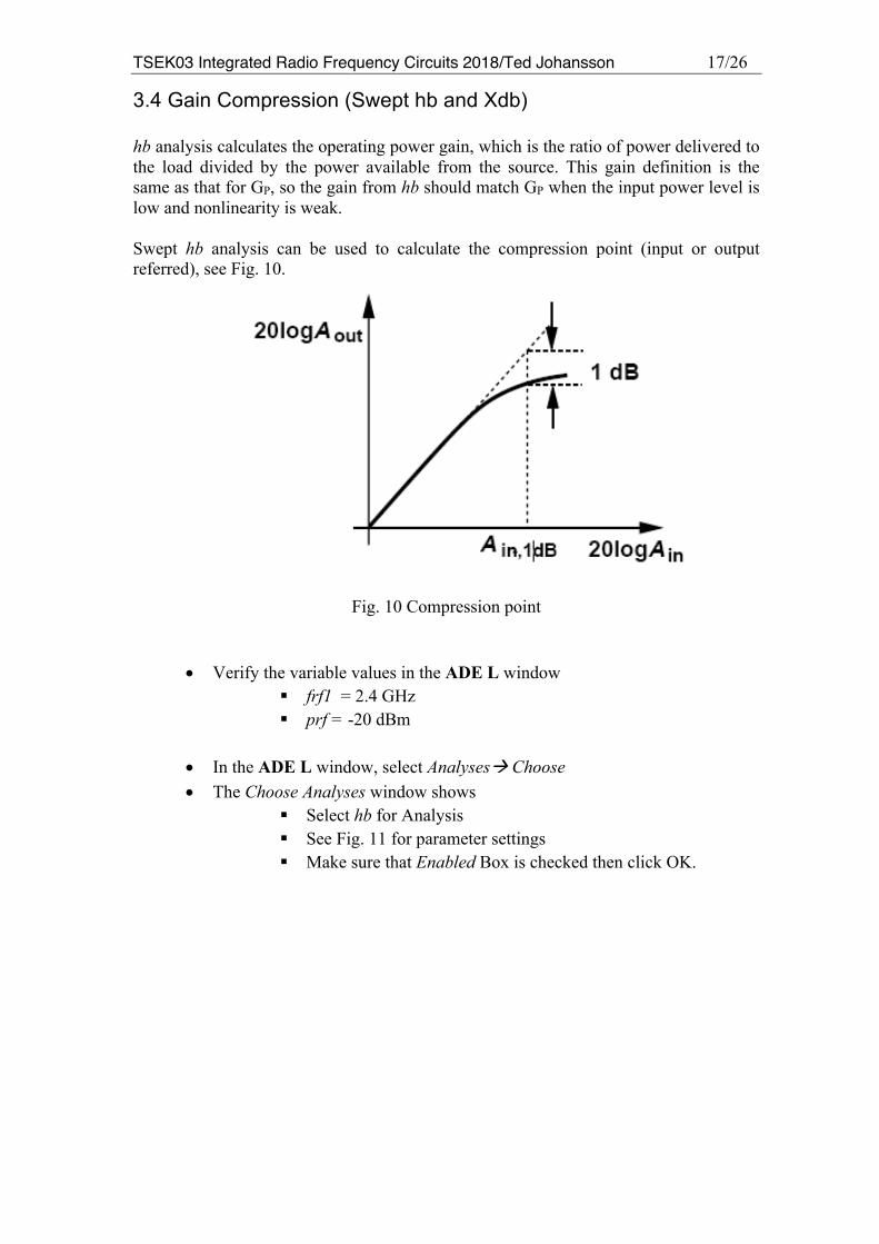
3.4 Gain Compression (Swept hb and Xdb) hb analysis calculates the operating power gain, which is the ratio of power delivered to the load divided by the power available from the source. This gain definition is the same as that for GP, so the gain from hb should match GP when the input power level is low and nonlinearity is weak. Swept hb analysis can be used to calculate the compression point (input or output referred), see Fig. 10.
Fig. 10 Compression point
• Verify the variable values in the ADE L window § frf1 = 2.4 GHz § prf = -20 dBm
• In the ADE L window, select Analysesà Choose • The Choose Analyses window shows
§ Select hb for Analysis § See Fig. 11 for parameter settings § Make sure that Enabled Box is checked then click OK.

TSEK03 Integrated Radio Frequency Circuits 2018/Ted Johansson 18/26
Fig 11. hb settings for swept analysis

TSEK03 Integrated Radio Frequency Circuits 2018/Ted Johansson 19/26
• In the ADE L window click on Simulationà Netlist and Run to start the simulation, make sure that simulation completes without too many errors in the log.
• The Direct Plot Form window shows
§ Analysis à hb § Function à Compression point § Format à Output Power § Compression point /Curve à Input-referred § 1st order Harmonic à 1 2.4G § Select the output port on the schematic § Compression curve and Compression point are automatically
plotted, see Fig. 12
Fig 12. Compression curve and Compression point
• How much is the output-referred compression point?
Starting from MMSIM13.1 (version number for the spectre simulator, the executable that runs the simulations), a dedicated Xdb compression option is integrated in the hb

TSEK03 Integrated Radio Frequency Circuits 2018/Ted Johansson 20/26 analysis form. It calculates compression points and compression curves directly, without the need for post processing or manual setup of power sweeps. It supports voltage and power-based compression point calculation. It is extremely useful when a large number of compression simulations are needed such as in the corner simulations or MC (Monte Carlo) analysis.
• Verify the variable values in the ADE L window § frf 1 = 2.4 GHz § prf = -20 dBm
• In the ADE L window, select Analysesà Choose • The Choose Analyses window shows
§ Select hb for Analysis § See Fig. 13 for general parameter settings § Check the Compression box and enter additional parameters
according to Fig. 14 § Make sure that Enabled Box is checked then click OK.
• In the ADE L window click on Simulationà Netlist and Run to start the
simulation, make sure that simulation completes without too many errors in the log.
• In the ADE L window, select Resultsà Direct Plotà Main Form • The Direct Plot Form window shows
§ Analysis à xdb § Function à Power/voltage/gain § Plot § Compression curve and Compression point are plotted, see Fig.
15

TSEK03 Integrated Radio Frequency Circuits 2018/Ted Johansson 21/26
Fig 13. hb settings

TSEK03 Integrated Radio Frequency Circuits 2018/Ted Johansson 22/26
Fig 14. Compression point settings in hb analysis
Fig 15. Compression curve and Compression point using Xdb analysis.
TSEK03 Integrated Radio Frequency Circuits 2018/Ted Johansson 23/26
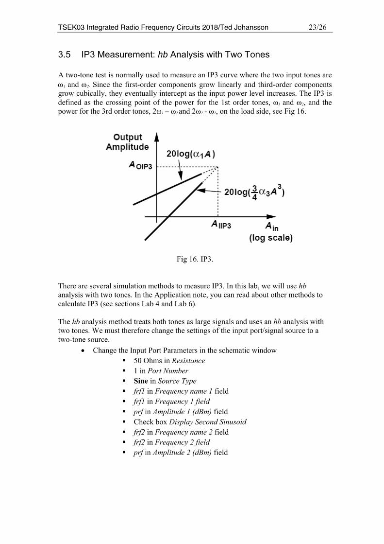
3.5 IP3 Measurement: hb Analysis with Two Tones A two-tone test is normally used to measure an IP3 curve where the two input tones are w1 and w2. Since the first-order components grow linearly and third-order components grow cubically, they eventually intercept as the input power level increases. The IP3 is defined as the crossing point of the power for the 1st order tones, ω1 and ω2, and the power for the 3rd order tones, 2ω1 – ω2 and 2ω2 - ω1, on the load side, see Fig 16.
Fig 16. IP3.
There are several simulation methods to measure IP3. In this lab, we will use hb analysis with two tones. In the Application note, you can read about other methods to calculate IP3 (see sections Lab 4 and Lab 6). The hb analysis method treats both tones as large signals and uses an hb analysis with two tones. We must therefore change the settings of the input port/signal source to a two-tone source.
• Change the Input Port Parameters in the schematic window § 50 Ohms in Resistance § 1 in Port Number § Sine in Source Type § frf1 in Frequency name 1 field § frf1 in Frequency 1 field § prf in Amplitude 1 (dBm) field § Check box Display Second Sinusoid § frf2 in Frequency name 2 field § frf2 in Frequency 2 field § prf in Amplitude 2 (dBm) field

TSEK03 Integrated Radio Frequency Circuits 2018/Ted Johansson 24/26
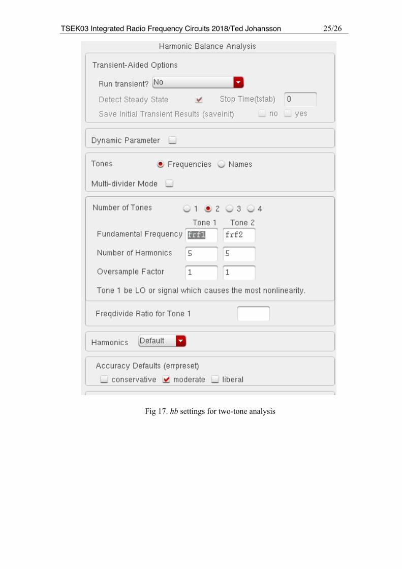
• Verify the variable values in the ADE L window § frf1 = 2.4 GHz § frf2 = 2.44 GHz § prf = -40 dBm
• In the ADE L window, select Analysesà Choose • The Choosing Analyses window shows
§ Select hb for Analysis § See Fig. 17 for the parameter settings § Make sure that Enabled Box is checked then click OK.
• Click OK In the ADE L window click on Simulationà Netlist and Run to
start the simulation, make sure that simulation completes without errors.
• In the ADE L window, select Resultsà Direct Plotà Main Form • The Direct Plot Form window shows
§ Function à IPN Curves § Select Port (Fixed R (Port)) § Single Point Input Power Value à -40 dB § Highlight Input Referred IP3 § Order à 3rd § 3rd Order Harmonic à 2.48G § 1st Order Harmonic à 2.4G § Activate the Schematic Window and click on Output port to
view the results as shown in Fig. 18.
TSEK03 Integrated Radio Frequency Circuits 2018/Ted Johansson 25/26
Fig 17. hb settings for two-tone analysis

TSEK03 Integrated Radio Frequency Circuits 2018/Ted Johansson 26/26
Fig. 18. Input-referred IIP3
• How much is the OIP3?
This concludes the LNA simulation lab!