tsv stress-aware full-chip mechanical reliability analysis ... · tsv stress-aware full-chip...
TRANSCRIPT

TSV Stress-aware Full-Chip Mechanical ReliabilityAnalysis and Optimization for 3D IC
Moongon Jung1, Joydeep Mitra2, David Z. Pan2, and Sung Kyu Lim1
1 School of ECE, Georgia Institute of Technology, Atlanta, GA, USA2 Department of ECE, University of Texas at Austin, Austin, TX, USA
[email protected], {joydeep, dpan}@ece.utexas.edu, [email protected]
ABSTRACTIn this work, we propose an efficient and accurate full-chip thermo-mechanical stress and reliability analysis tool and design optimiza-tion methodology to alleviate mechanical reliability issues in 3DICs. First, we analyze detailed thermo-mechanical stress inducedby TSVs in conjunction with various associated structures such aslanding pad and dielectric liner. Then, we explore and validatethe use of the linear superposition principle of stress tensors anddemonstrate the accuracy of this method against detailed finite el-ement analysis (FEA) simulations. Next, we apply this linear su-perposition method to full-chip stress simulation and a reliabilitymetric named the von Mises yield criterion. Finally, we propose adesign optimization methodology to mitigate the mechanical reli-ability problems in 3D ICs. Our experimental results demonstratethe effectiveness of our methodology.
Categories and Subject Descriptors
General TermsDesign
Keywords3D IC, TSV, stress, mechanical reliability
1. INTRODUCTIONDue to the coefficients of thermal expansion (CTE) mismatch be-
tween a TSV fill material such as copper (Cu) and silicon substrate,thermo-mechanical stress is induced during fabrication process andthermal cycling of TSV structures, which can affect device perfor-mance [7] or drive crack growth in 3D interconnects [4, 6]. Mostprevious works focused on modeling the thermo-mechanical stressand reliability of a single TSV in isolation. These simulations areperformed using FEA methods which are computationally expen-sive or infeasible for full-chip analysis. Furthermore, some worksused unrealistic TSV structures such as an extremely large landingpad (LP), mainly because the design context is not considered.
Even though there are several works on thermo-mechanical relia-bility issues induced by TSV stress, this is the first work addressingTSV thermo-mechanical stress and reliability issues on a full-chipscale to the best of our knowledge. In this paper, we propose a TSVthermo-mechanical stress and reliability analysis flow as well as a
Permission to make digital or hard copies of all or part of this work forpersonal or classroom use is granted without fee provided that copies arenot made or distributed for profit or commercial advantage and that copiesbear this notice and the full citation on the first page. To copy otherwise, torepublish, to post on servers or to redistribute to lists, requires prior specificpermission and/or a fee.DAC ’11, Jun 05-10 2011, San Diego, California, USACopyright 2011 ACM 978-1-4503-0636-2/11/06 ...$10.00.
Figure 1: Baseline TSV structure. (a) 4X TSV cell that occupies4 standard cell rows (KOZ = 2.44 µm). (b) 3X TSV cell (KOZ= 1.205 µm).
design optimization methodology to reduce mechanical reliabilityproblems in TSV based 3D ICs. We use von Mises yield criterionas a mechanical reliability metric, and show impacts of design pa-rameters such as TSV size, landing pad size, liner thickness andkeep-out-zone (KOZ) size on the mechanical reliability.
The main contributions of this work include the following: (1)Modeling: Compared with existing works, we simulate more de-tailed and realistic TSV structures and study their impact on stressas well as a mechanical reliability metric. We also model the impactof chip operating temperature on stress and reliability. (2) Full-chipanalysis: We, for the first time, validate the principle of linear su-perposition of stress tensors against FEA simulations, and applythis methodology to generate a stress map and a reliability metricmap on a full-chip scale. (3) Design optimization: We present de-sign methods to reduce von Mises stress, which is a mechanicalreliability metric, on full-chip 3D IC designs by tuning design pa-rameters such as landing pad size, liner thickness, KOZ size, andTSV placement.
2. DETAILED BASELINE MODELINGThe analytical 2D radial stress model, known as Lame stress so-
lution, was employed to address the TSV thermo-mechanical stresseffect on device performance in [7]. Even though this closed-formformula is easy to handle, it does not capture the 3D nature of astress field near a wafer surface around TSVs where devices arelocated [6]. Moreover, the TSV/substrate interface region near thewafer surface is known to be a highly problematic area for mechan-
B.7.2 [Hardware, Integrated Circuits]: Design Aids
188
12.1

TSV liner
landing pad edge
TS
V
Figure 2: Effect of TSV structures on σrr stress.
ical reliability [6]. In our study, wafer surface means the siliconsurface right below substrate (Si)/dielectric layer (SiO2) interface.
Though the authors in [6] proposed a semi-analytic 3D stressmodel, it is only valid for a TSV with a high aspect ratio. Fur-thermore, since their model is only applicable to a single TSV inisolation and their TSV structure only includes TSV and siliconsubstrate, it cannot be directly used to assess mechanical reliabilityissues in a full-chip scale as well as a TSV which contains a land-ing pad and a dielectric liner because of the change in boundaryconditions.
2.1 3D FEA SimulationSince there is no known analytical stress model for a realistic
TSV structure, 3D FEA models for a TSV structure are created toinvestigate the stress distribution near wafer surface. To realisti-cally examine the thermo-mechanical stress induced by TSVs, ourbaseline simulation structure of a TSV is based on the fabricatedand the published data [1], as shown in Figure 1. We construct twoTSV cells, i.e. 4X TSV and 3X TSV, which occupy four and threestandard cell rows in 45 nm technology. We define 2.44 µm and1.205 µm from TSV edge as keep-out-zone (KOZ) in which nocell is allowed to be placed for TSV 4X and TSV 3X cells, respec-tively. Our baseline TSV diameter, height, landing pad size, andliner thickness are 5 µm, 30 µm, 6 µm, and 125 nm, respectively,unless specified, which are close to the data in [1]. We use SiO2 asa baseline liner material, and ignore Cu diffusion barrier materialsuch as Ta and Ti in these experiments since this barrier thicknessis negligible compared to SiO2 liner, hence its impact on stress dis-tribution is negligible. Material properties used for our experimentsare as follows: CTE (ppm/K) for Cu = 17, Si = 2.3, SiO2 = 0.5, andBCB = 40; Young’s modulus (GPa) for Cu = 110, Si = 130, SiO2
= 71, and BCB = 3. We use the FEA simulation tool ABAQUSto perform experiments, and all materials are assumed to be linearelastic.
Before discussing the detailed stress modeling results, we intro-duce the concept of a stress tensor. Stress at a point in an object canbe defined by the nine-component stress tensor:
σ = σij =
[σ11 σ12 σ13
σ21 σ22 σ23
σ31 σ32 σ33
]The first index i indicates that the stress acts on a plane normal to
the axis, and the second index j denotes the direction in which thestress acts. If index i and j are same we call this a normal stress,otherwise a shear stress. Since we adopt a cylindrical coordinatesystem in this modeling, index 1, 2, and 3 represent r, θ, and z,respectively.
2.2 Impact of TSV Liner and Landing PadFigure 2 shows FEA simulation results of a normal stress com-
ponent σrr along an arbitrary radial line from the TSV center atthe wafer surface with -250◦C of thermal load. That is, we assumeTSV structure is annealed at 275◦C and cooled down to 25◦C to
125nm liner edge
500nm liner edge
SiO2 liner (t = 125nm)
SiO2 liner (t = 500nm)
BCB liner (t = 125nm)
BCB liner (t = 500nm)
Figure 3: Effect of liner material/thickness on σrr stress.
mimic the manufacturing process [2, 5, 6]. We also assume thatthe entire TSV structure is stress free at the annealing temperature.We first observe the huge discrepancy between 2D solution and 3Dstress results at the TSV edge. It is widely known that most of me-chanical reliability failures occur at the interface between differentmaterials. Therefore, 2D solution does not predict mechanical fail-ure mechanism for TSVs correctly. Also, SiO2 liner, which acts asa stress buffer layer, reduces σrr stress at the TSV edge by 35 MPacompared with the case without landing pad and liner. The landingpad also helps decrease stress magnitude at the TSV edge.
We also employ benzocyclobutene (BCB), a polymer dielectricmaterial, as an alternative TSV liner material [5, 6]. Since Young’smodulus, which is a measure of the stiffness of an isotropic elasticmaterial, of BCB is much lower than Cu, Si, and SiO2, this BCBliner can absorb the stress effectively from the CTE mismatch. Fig-ure 3 shows the impact of liner material and thickness on σrr stresscomponent. As liner thickness increases, stress magnitude at theTSV edge decreases noticeably, especially for the BCB liner case.
It is evident from these experiments that modeling stress dis-tribution considering surrounding structures such as a liner and alanding pad is important to analyze the thermo-mechanical stressaround TSVs more accurately. We construct a stress library byvarying TSV diameter/height, landing pad size, and liner mate-rial/thickness to enable full-chip thermo-mechanical stress and re-liability analysis with different TSV structures.
3. FULL-CHIP RELIABILITY ANALYSISFEA simulation of thermo-mechanical stress for multiple TSVs
require huge computing resources and time, thus it is not suitablefor full-chip analysis. In this section, we present full-chip stressand reliability analysis flow. To enable a full-chip stress analysis,we first explore and validate the principle of linear superpositionof stress tensors from individual TSVs. Based on the linear su-perposition method, we build full-chip stress map. Then from thisfull-chip stress map, we compute von Mises yield metric to predictmechanical reliability problems in 3D ICs.
3.1 Full-chip Analysis with Multiple TSVsFirst, based on the observation that the stress field of a single
TSV in isolation is radially symmetrical due to the cylindrical shapeof a TSV, we obtain stress distribution around a TSV from a set ofstress tensors along an arbitrary radial line from the TSV centerin a cylindrical coordinate system. To evaluate a stress tensor at apoint affected by multiple TSVs, a conversion of a stress tensor toa Cartesian coordinate system is required. This is due to the factthat we extract stress tensors from a TSV whose center is the originin the cylindrical coordinate system; hence we cannot perform avector sum of stress tensors at a point from each TSV which has adifferent center location. Then, we compute a stress tensor at thepoint of interest by adding up stress tensors from TSVs affectingthis point. We set a TSV stress influence zone as 25 µm from thecenter of a TSV, since the magnitude of stress components becomes
189
12.1

-350
-290
-230
-170
-110
-60
0
50
100
150
200
(MPa)
(a) (b)
str
ess (
MP
a)
200
180
160
140
120
100
80
60
40
20
00 1 2 3 4 5 6 7 8 9 10
(c)
Center of the top-left TSV
Center of the top-right TSV
FEA
ours
Figure 4: Sample stress comparison between FEA simulation and linear superposition method. (a) FEA result (σxx). (b) ours (σxx).(c) FEA vs. ours (σxx) along the white line in (a).
σv =
√(σxx − σyy)2 + (σyy − σzz)2 + (σzz − σxx)2 + 6(σ2
xy + σ2yz + σ2
zx)
2(1)
negligible beyond this distance.Let the stress tensor in Cartesian and cylindrical coordinate sys-
tem be Sxyz and Srθz , respectively.
Sxyz =
[σxx σxy σxz
σyx σyy σyz
σzx σzy σzz
], Srθz =
[σrr σrθ σrz
σθr σθθ σθz
σzr σzθ σzz
]The transform matrix Q is the form:
Q =
[cos θ − sin θ 0sin θ cos θ 00 0 1
]where, θ is the angle between the x-axis and a line from the TSVcenter to the simulation point. A stress tensor in a cylindrical co-ordinate system can be converted to a Cartesian coordinate systemusing conversion matrices: Sxyz = QSrθzQ
T .We validate the linear superposition of stress tensors against FEA
simulations by varying the number of TSVs and their arrangement.We observe that % error between the linear superposition methodand FEA simulations is less than 5 % down to the TSV pitch of 7µm. As we further decrease TSV pitch, due to strong TSV-to-TSVinteraction % error starts to increase. However, since the minimumTSV pitch achievable in the current process is around 10 µm [1],this linear superposition method is valid in a practical sense. Fig-ure 4 shows one of test cases which contains three TSVs, and itclearly shows our linear superposition method matches well withthe FEA simulation result. Even though we only show σxx compo-nent due to space limit, other stress tensor components also matchwell with FEA simulation results.
3.2 Mechanical Reliability AnalysisIn order to evaluate if computed stresses indicate possible relia-
bility concerns, a critical value for a potential mechanical failuremust be chosen. The von Mises yield criterion is known to beone of the most widely used mechanical reliability metric [8]. Ifthe von Mises stress exceeds a yielding strength, material yield-ing starts. Prior to the yielding strength, the material will deformelastically and will return to its original shape when the appliedstress is removed. However, if the von Mises stress exceeds theyield point, some fraction of the deformation will be permanentand non-reversible.
There is a large variation of yield strength of Cu in the literature,from 225 MPa to 600 MPa, and it has been reported to dependupon thickness, grain size, and temperature [8]. We use 600 MPaas a Cu yielding strength in our experiments. The yield strength ofsilicon is 7000 MPa, which will not be reliability concerns for thevon Mises yield criterion.
input : TSV list T , stress library, thermal map (optional)output: stress map, von Mises stress mapfor each TSV t in T do
c←− center of tr ←− FindStressInfluenceZone(c)for each point r′ in r do
r′.TSV ←− tend
endfor each simulation point p do
if p.TSV = ∅ thenfor each t ∈ p.TSV do
d←− distance(t, p)Scyl ←− FindStressTensor(d, temperature)θ ←− FindAngle(line tp, x axis)Q←− SetConversionMatrix(θ)SCart ←− QScylQ
T
p.SCart ←− p.SCart + SCart
endendvonMises(p)←− ComputeVonMises(p.Scart)
endAlgorithm 1: Full Chip Stress and Reliability Analysis Flow
The von Mises stress is a scalar value at a point that can be com-puted using components of a stress tensor shown in Equation (1).By evaluating von Mises stress at the interface between a TSV anda liner, where highest von Mises stress occurs, we can predict me-chanical failures in TSVs.
Our full-chip stress and reliability analysis flow is shown in Al-gorithm 1. We first start to find a stress influence zone from eachTSV. Then, we associate the points in the influence zone with theaffecting TSV. Next, for each simulation point under consideration,we look up the stress tensor from the TSV found in the associationstep, and use the coordinate conversion matrices to obtain stresstensors in the Cartesian coordinate system. We visit an individualTSV affecting this simulation point and add up their stress contri-butions. Once we finish the stress computation at a point, we obtainthe von Mises stress value using Equation (1). The complexity ofthis algorithm is O(n), where n is number of simulation points.
4. FULL-CHIP SIMULATION RESULTSWe implement a TSV-aware full-chip stress and reliability anal-
ysis flow in JAVA and C++. Four variations of an industrial circuit,
190
12.1

Table 1: Benchmark circuitsTSV TSV cell size wirelength area
circuit placement (µm× µm) (mm) (µm× µm)Irreg3X Irregular 7.41× 7.41 9060 960× 960Reg3X Regular 7.41× 7.41 9547 960× 960Irreg4X Irregular 9.88× 9.88 8884 1000× 1000Reg4X Regular 9.88× 9.88 9648 1000× 1000
Figure 5: Impact of TSV structure, TSV placement style, andKOZ size on the maximum von Mises stress. (a) designs with3X TSV cell (KOZ = 1.205 µm). (b) 4X TSV cell (KOZ = 2.44µm).
with changes in TSV placement style and TSV cell size, are usedfor our analysis, which are listed in Table 1. The number of TSVsand gates are 1472 and 370K, respectively, for all cases. Thesecircuits are synthesized using Synopsys Design Compiler with thephysical library of 45 nm technology, and designed using CadenceSoC Encounter to two-die stacked 3D ICs.
In the regular TSV placement scheme, we pre-place TSVs uni-formly on each die, and then place cells, while TSVs and cells areplaced simultaneously in the irregular TSV placement scheme. Theirregular TSV placement shows better wirelength than the regularcase [3]. We use a gate-level 3D IC design methodology for thesecircuits as a baseline, and compare these with block-level designsin section 4.6.
Even though we simulate 25M points for all test cases, it takesless than 10 minutes since this requires a linear time computationproportional to the number of simulation points on the grid, while atypical FEA simulation for a single TSV structure takes from sev-eral minutes to hours depending on the mesh structure. We alsovalidate our analysis results against FEA simulations by compar-ing a small section of a design which contains a small group ofTSVs, which shows less than 2% error in terms of the maximumstress value. The proposed full-chip stress and reliability analysisbased on linear superposition of stress tensors is fast and accurateenough to be used for iterative optimization purpose.
4.1 Overall ComparisonIn this section, we discuss the impact of TSV structure, TSV
placement style, and KOZ size on the thermo-mechanical stress
Figure 6: Close-up shots of layouts and von Mises stress maps.(a) Irreg3X. (b) Reg3X. (c) Von Mises stress map of Irreg3X.(d) Von Mises stress map of Reg3X.
Table 2: Impact of TSV size on the maximum von Mises stress.The numbers in parentheses are % reduction compared to TSVlarge case.
max von Mises stress (MPa)TSV placement TSV large TSV medium TSV smallIrregular 1241.87 1141.9 (8% ↓) 924.16 (26% ↓)Regular 754.9 659.37 (12% ↓) 456.47 (40% ↓)
and the mechanical reliability in 3D ICs. We perform full-chipstress and reliability analysis on our benchmark circuits based onour stress modeling results with different TSV structures.
Figure 5 shows the maximum von Mises stress in our bench-mark circuits. We first observe that designs with irregular TSVplacement show worse maximum von Mises stress than those withthe regular TSV placement. This is mainly because TSVs can beplaced closely in case of the irregular TSV placement scheme tominimize wirelength. Figure 6 shows the part of von Mises stressmaps of Irreg3X and Reg3X circuits, and we see that most of TSVsin the Irreg3X circuit exceed Cu yielding strength (600 MPa). Sec-ond, as the KOZ size becomes larger stress level reduces signifi-cantly for the irregular TSV placement case. By enlarging KOZsize, interference from nearby TSVs is reduced. However, for theregular TSV placement case, since TSV pitch of Reg3X (23.5 µm)and Reg4X (25 µm) is similar and also interference from nearbyTSVs is negligible at this distance, there is no noticeable differencein maximum von Mises stress. Third, these results show the impor-tance of using an accurate TSV stress model to assess the mechani-cal reliability of 3D ICs. There are significant differences in the vonMises stress depending on the existence of structures surroundinga TSV, such as a landing pad or a liner. It is possible that we mightoverestimate the reliability problems by using a simple TSV stressmodel not considering a landing pad or a liner. However, most ofthese test cases violate the von Mises yield criterion for Cu TSV.Section 4.4 shows how TSV liners help reduce the violations.
4.2 Impact of TSV SizeTo investigate the effect of the TSV size, we use three different
sizes of TSV with a same aspect ratio of 6; TSV small (H/D =15/2.5 µm), TSV medium (H/D = 30/5 µm), and TSV large(H/D = 60/10 µm), where H/D is TSV height/diameter. Also,
191
12.1

Table 3: Impact of a landing pad size on von Mises criterion.The numbers in parentheses are % reduction compared to LP6× 6 µm2 case.
LP 6× 6 µm2 LP 8× 8 µm2
max von Mises # violating max von Mises # violatingcircuit stress (MPa) TSVs stress (MPa) TSVsIrreg4X 852.83 1472 827.06 (3% ↓) 1472 (0% ↓)Reg4X 659.84 1472 612.45 (7% ↓) 1472 (0% ↓)
Table 4: Impact of liner thickness on the number of TSVs vio-lating von Mises criterion. The numbers in parentheses are %reduction compared to the 125 nm thick liner case.
liner # violating TSVscircuit material 125 nm 250 nm 500 nmIrreg3X SiO2 1467 1433 (2% ↓) 1297 (11% ↓)
BCB 1407 1172 (17% ↓) 357 (75% ↓)Reg3X SiO2 1472 0 (100% ↓) 0 (100% ↓)
BCB 0 0 (-) 0 (-)Irreg4X SiO2 1472 1272 (14% ↓) 97 (93% ↓)
BCB 1044 535 (49% ↓) 0 (100% ↓)Reg4X SiO2 1472 0 (100% ↓) 0 (100% ↓)
BCB 0 0 (-) 0 (-)
to suppress the effect of KOZ size, we use 2X TSV cell (KOZ1.22 µm) for TSV small, 3X TSV cell (KOZ 1.202 µm) for TSVmedium, and 5X TSV cell (KOZ 1.175 µm) for TSV large. Ad-ditionally, we set the landing pad width is 1 µm larger than thecorresponding TSV diameter, and use a 125 nm thick SiO2 linerfor all cases for fair comparisons. Table 2 shows the maximumvon Mises stress. For both irregular and regular TSV placementschemes benefit from smaller TSV diameter significantly. This ismainly because the magnitude of normal stress components decayproportional to (D/2r)2, where r is the distance from the TSVcenter.
4.3 Impact of Landing Pad SizeIn this section, we explore the impact of landing pad size, which
is normally determined by considering TSV alignment, on reliabil-ity issues. Designs with 4X TSV cells with 125 nm thick SiO2
liner are used. We compare the maximum von Mises stress andthe number of violating TSVs with two different landing pad sizeshown in Table 3. These results show that the regular TSV place-ment benefits more von Mises stress reduction from the larger land-ing pad size. This is because the stress reduction in a single TSVdirectly translates to the overall stress magnitude decrease in a full-chip scale for the regular TSV placement case. However, increas-ing the landing pad size does not improve von Mises stress signifi-cantly. Also we see that all TSVs do not satisfy von Mises criterionfor every test case. This is because only the magnitude of σrr stresscomponent at the wafer surface is reduced due to Cu landing pad,while other stress components hardly changes with a larger landingpad size.
4.4 Impact of Liner ThicknessIn this section, we examine the impact of liner thickness on von
Mises stress. We use designs with both 3X TSV cells and 4X TSVcells, and set the landing pad size 6×6 µm2 and 8×8 µm2, respec-tively. Figure 7 shows the maximum von Mises stress results withliner thickness of 125 nm, 250 nm, and 500 nm. We observe thatliner thickness has a huge impact on the von Mises stress magni-tude, since the thicker liner effectively absorbs thermo-mechanicalstress at the TSV/liner interface. Especially, the BCB liner showssignificant reduction in the maximum von Mises stress comparedwith SiO2 liner due to extremely low Young’s modulus shown inSection 2.1. For example, 500 nm thick BCB liner reduces themaximum von Mises stress by 29% for the Irreg3X and satisfiesthe von Mises yield criterion for all circuits with a regular TSVplacement.
Table 4 shows the number of TSVs violating von Mises criterion.
Figure 7: Impact of liner thickness on the maximum von Misesstress of circuits with 3X TSV cell.
60
55
50
45
Figure 8: Impact of temperature (◦C) during a chip operationon von Mises stress. (a) layout of Reg3X. TSV landing pads arewhite rectangles. (b) thermal map.
Even though there are still many TSVs not satisfying von Misescriterion for the Irreg3X circuit, it is possible to reduce von Misesstress if we place TSVs carefully considering this reliability metricduring a placement stage.
4.5 Impact of Chip Operation TemperatureUp to this point, we only consider the residual stress caused by
the manufacturing process. In this section, we examine the reliabil-ity problem during the chip operation phase. Our full-chip thermalsimulation flow is as follows. We first generate a power map usingSoC Encounter, and then feed this to ANSYS Fluent with in-houseadd-ons which enable a steady-state thermal analysis for GDSIIlevel 3D ICs shown in Figure 8(b). Depending on the temperaturedistribution across the die area, each TSV experiences a differentthermal load. Thus, the significance of mechanical reliability prob-lems of an individual TSV might be different from each other. Tosupport temperature dependent stress analysis, we build stress li-brary with wide range of thermal load.
We use the Reg3X circuit for this experiment since TSVs in theregular TSV placement scheme show uniform von Mises stress dis-tribution, which enables us to observe the impact of an operatingtemperature across the die easily. We use a 500 nm thick BCBliner for this experiment. The cool spot experiences higher vonMises stress, since the temperature difference from the stress freetemperature, 275◦C in our case, is larger in the cool spot than inthe hot spot. However, since the maximum temperature differenceacross the die is only 20◦C, the impact of an operating tempera-ture on the TSV reliability across the die is not significant. In ourtest case, the difference of the maximum von Mises stress betweentwo spots is 31.8 MPa. Also, both the hot and the cool spot ex-perience less maximum von Mises stress compared to the residualstress case, again due to the reduced thermal load. However, thereduction of von Mises stress during a chip operation cannot re-cover the material yielding failure if it already exists, since this is a
192
12.1
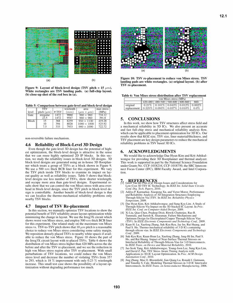
Figure 9: Layout of block-level design (TSV pitch = 15 µm).White rectangles are TSV landing pads. (a) full-chip layout.(b) close-up shot of the red box in (a).
Table 5: Comparison between gate-level and block-level designTSV wirelenth area max stress
level pitch (µm) # TSV (mm) (µm× µm) (MPa)Gate irregular 1472 9060 960× 960 734.12
23.5 1472 9547 960× 960 391.8Block 15 368 8259 950× 1130 419.28
10 394 8028 1080× 1000 525.927.5 333 7933 980× 1090 722.72
non-reversible failure mechanism.
4.6 Reliability of Block-Level 3D DesignEven though the gate-level 3D design has the potential of high-
est optimization, the block-level design is attractive in the sensethat we can reuse highly optimized 2D IP blocks. In this sec-tion, we study the reliability issues in block-level 3D designs. 3Dblock-level designs are generated using an in-house 3D floorplan-ner which treats a group of TSVs as a block shown in Figure 9.We use a 500 nm thick BCB liner for this experiment. We varythe TSV pitch inside TSV blocks to examine its impact on lay-out quality as well as reliability issues. Table 5 shows that block-level designs use less number of TSVs, show shorter wirelength,and occupy more area than gate-level designs. Experimental re-sults show that we can control the von Mises stress with area over-head in block-level design, since the TSV pitch in block-level de-sign is controllable. Another benefit of block-level design is thatwe can localize the thermo-mechanical reliability problems onlynearby TSV blocks.
4.7 Impact of TSV Re-placementIn this section, we manually optimize TSV locations to show the
potential benefit of TSV reliability aware layout optimization whileminimizing the change in layout. We use the Irreg3X circuit whichshows worst von Mises stress, and employ 500 nm thick BCB linerfor this experiment. Our related study on the maximum von Misesstress vs. TSV-to-TSV pitch shows that 10 µm pitch is a reasonablechoice to reduce von Mises stress considering some safety margin.We reposition densely placed TSVs to nearby white spaces if avail-able to reduce the von Mises stress. Figure 10 shows the part ofthe Irreg3X circuit layout with re-placed TSVs. Table 6 shows thedistribution of von Mises stress higher than 420 MPa across the diebefore and after the TSV re-placement, and we see the reduction inhigh von Mises stress region after TSV re-placement. With smallperturbations of TSV locations, we could reduce the von Misesstress level and decrease the number of violating TSVs from 357to 293, which is 18 % improvement with only 0.23 % wirelengthincrease. This small test case shows the possibility of a layout op-timization without degrading performance too much.
Figure 10: TSV re-placement to reduce von Mises stress. TSVlanding pads are white rectangles. (a) original layout. (b) afterTSV re-placement.
Table 6: Von Mises stress distribution after TSV replacementvon Mises stress (MPa)
420-480 480-540 540-600 600-660 660-original 0.21% 0.101% 0.043% 0.012% 0.002%replacement 0.225% 0.093% 0.037% 0.010% 0.0%
5. CONCLUSIONSIn this work, we show how TSV structures affect stress field and
a mechanical reliability in 3D ICs. We also present an accurateand fast full-chip stress and mechanical reliability analysis flow,which can be applicable to placement optimization for 3D ICs. Ourresults show that KOZ size, TSV size, liner material/thickness, andTSV placement are key design parameters to reduce the mechanicalreliability problems in TSV based 3D ICs.
6. ACKNOWLEDGMENTSWe would like to acknowledge Dae Hyun Kim and Krit Athikul-
wongse for providing their 3D floorplanner and thermal analyzer.This work is supported in part by the National Science Foundationunder Grants No. CCF-1018216, CCF-1018750, the SRC Intercon-nect Focus Center (IFC), IBM Faculty Award, and Intel Corpora-tion.
7. REFERENCES[1] Geert Van der Plas et al. Design Issues and Considerations for
Low-Cost 3D TSV IC Technology. In IEEE Int. Solid-State CircuitsConf. Dig. Tech. Papers, 2010.
[2] Aditya P. Karmarkar, Xiaopeng Xu, and Victor Moroz. Performanceand Reliability Analysis of 3D-Integration Structures EmployingThrough Silicon Via (TSV. In IEEE Int. Reliability PhysicsSymposium, 2009.
[3] Dae Hyun Kim, Krit Athikulwongse, and Sung Kyu Lim. A Study ofThrough-Silicon-Via Impact on the 3D Stacked IC Layout. In Proc.IEEE Int. Conf. on Computer-Aided Design, 2009.
[4] Xi Liu, Qiao Chen, Pradeep Dixit, Ritwik Chatterjee, Rao R.Tummala, and Suresh K. Sitaraman. Failure Mechanisms andOptimum Design for Electroplated Copper Through-Silicon Vias(TSV). In IEEE Electronic Components and Technology Conf., 2009.
[5] Kuan H. Lu, Xuefeng Zhang, Suk-Kyu Ryu, Jay Im, Rui Huang, andPaul S. Ho. Thermo-mechanical reliability of 3-D ICs containingthrough silicon vias. In IEEE Electronic Components and TechnologyConf., 2009.
[6] Suk-Kyu Ryu, Kuan-Hsun Lu, Xuefeng Zhang, Jang-Hi Im, Paul S.Ho, and Rui Huang. Impact of Near-Surface Thermal Stresses onInterfacial Reliability of Through-Silicon-Vias for 3-D Interconnects.In IEEE Trans. on Device and Material Reliability, 2010.
[7] Jae-Seok Yang, Krit Athikulwongse, Young-Joon Lee, Sung Kyu Lim,and David Z. Pan. TSV Stress Aware Timing Analysis withApplications to 3D-IC Layout Optimization. In Proc. ACM DesignAutomation Conf., 2010.
[8] Jing Zhang, Max O. Bloomfield, Jian-Qiang Lu, Ronald J. Gutmann,and Timothy S. Cale. Modeling Thermal Stresses in 3-D IC InterwaferInterconnects. In IEEE Trans. on Semiconductor Manufacturing, 2006.
193
12.1