tubingen, 9 november 2005c.cattadori infn milano & lngs gerda meeting tg3 status report on...
TRANSCRIPT

Tubingen, 9 November 2005 C.Cattadori INFN Milano & LNGS GERDA meeting
TG3 Status Report On behalf of TG3 working group

Tubingen, 9 November 2005 C.Cattadori INFN Milano & LNGS GERDA meeting
The front-end solutions for GERDA
Existing devices under test for GERDA: OK for PHASE I
• BF862 FET (inside LN bath) + Milano-Agata Hybrid preamplifiers (outside LN bath)
• Integrated monolithic JFET preamplifier IPA4 with internal or with external JFET. (both inside LN bath)
• BF862 + Amptek 250 preamplifier (both inside LN bath)
R&D on ASIC CMOS Circuits. Maybe ready for Phase I, necessary for PHASE II
Tubingen, 9 November 2005 C.Cattadori INFN Milano & LNGS GERDA meeting
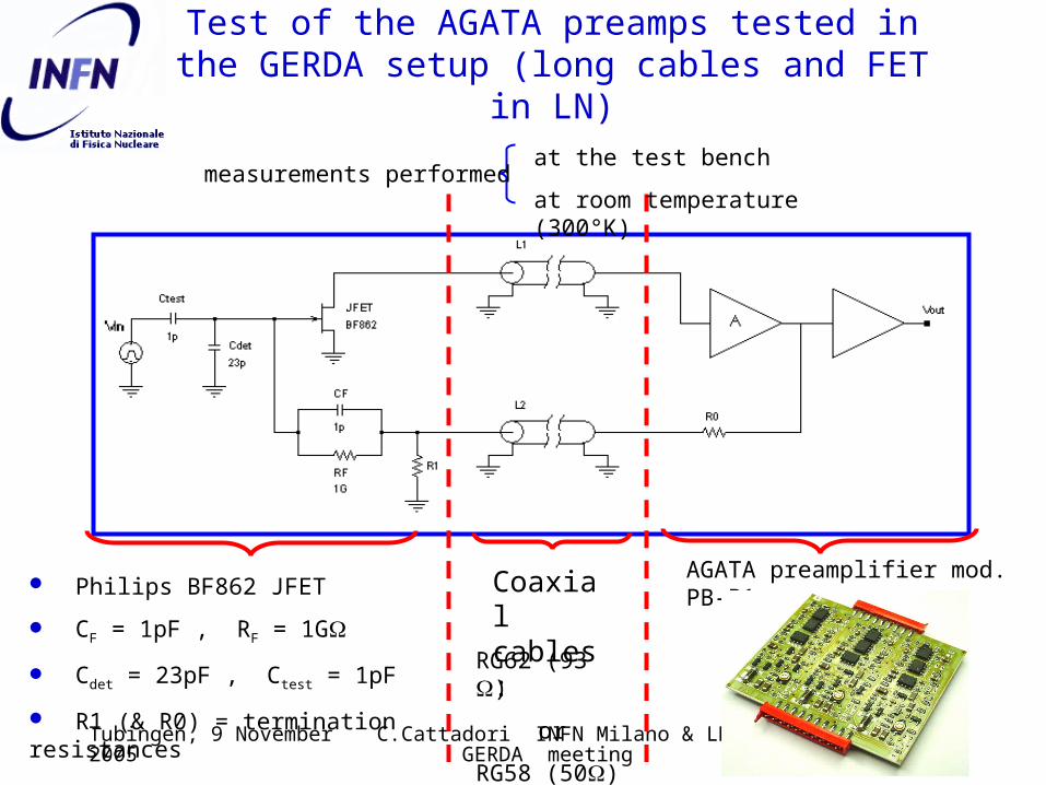
Test of the AGATA preamps tested in the GERDA setup (long cables and FET in LN)
Coaxial cables :
Philips BF862 JFET
CF = 1pF , RF = 1G
Cdet = 23pF , Ctest = 1pF
R1 (& R0) = termination resistances
RG62 (93 )
or
RG58 (50)
AGATA preamplifier mod. PB-B1
at the test bench
at room temperature (300°K)
measurements performed
Tubingen, 9 November 2005 C.Cattadori INFN Milano & LNGS GERDA meeting
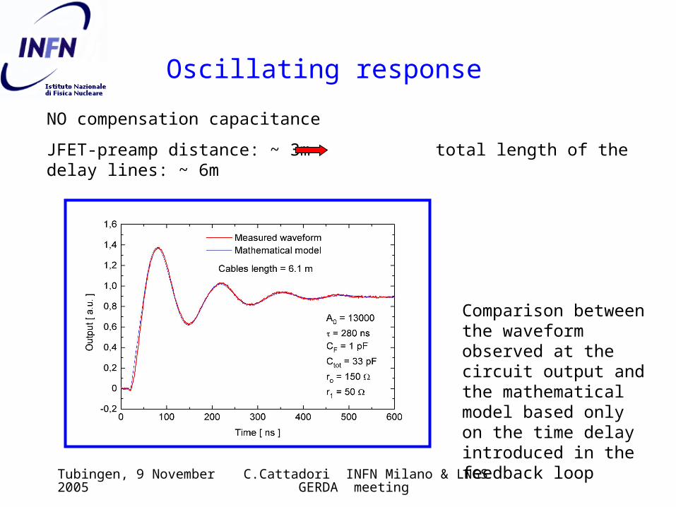
Oscillating response
NO compensation capacitance
JFET-preamp distance: ~ 3m total length of the delay lines: ~ 6m
Comparison between the waveform observed at the circuit output and the mathematical model based only on the time delay introduced in the feedback loop
Tubingen, 9 November 2005 C.Cattadori INFN Milano & LNGS GERDA meeting
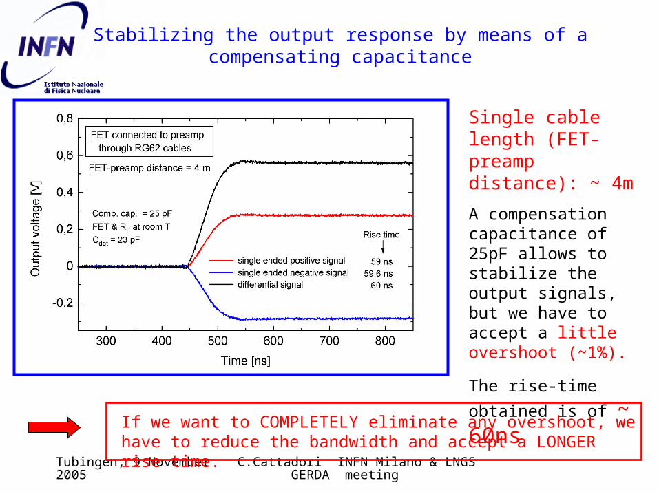
Stabilizing the output response by means of a compensating capacitance
Single cable length (FET-preamp distance): ~ 4m
A compensation capacitance of 25pF allows to stabilize the output signals, but we have to accept a little overshoot (~1%).
The rise-time
obtained is of ~ 60nsIf we want to COMPLETELY eliminate any overshoot, we have
to reduce the bandwidth and accept a LONGER rise time.

Tubingen, 9 November 2005 C.Cattadori INFN Milano & LNGS GERDA meeting
Comparison of RG62 with RG58 cables to connect JFEt to the amplifier
Rise time values vs. different FET-preamp distances in complete absence of any overshoot
Better performance of RG62 (93 ohm) cables !
The main cause is the difference in the time delay they introduced in the signal transmission:
RG62: 4 ns/m
RG58: 5 ns/m
Tubingen, 9 November 2005 C.Cattadori INFN Milano & LNGS GERDA meeting
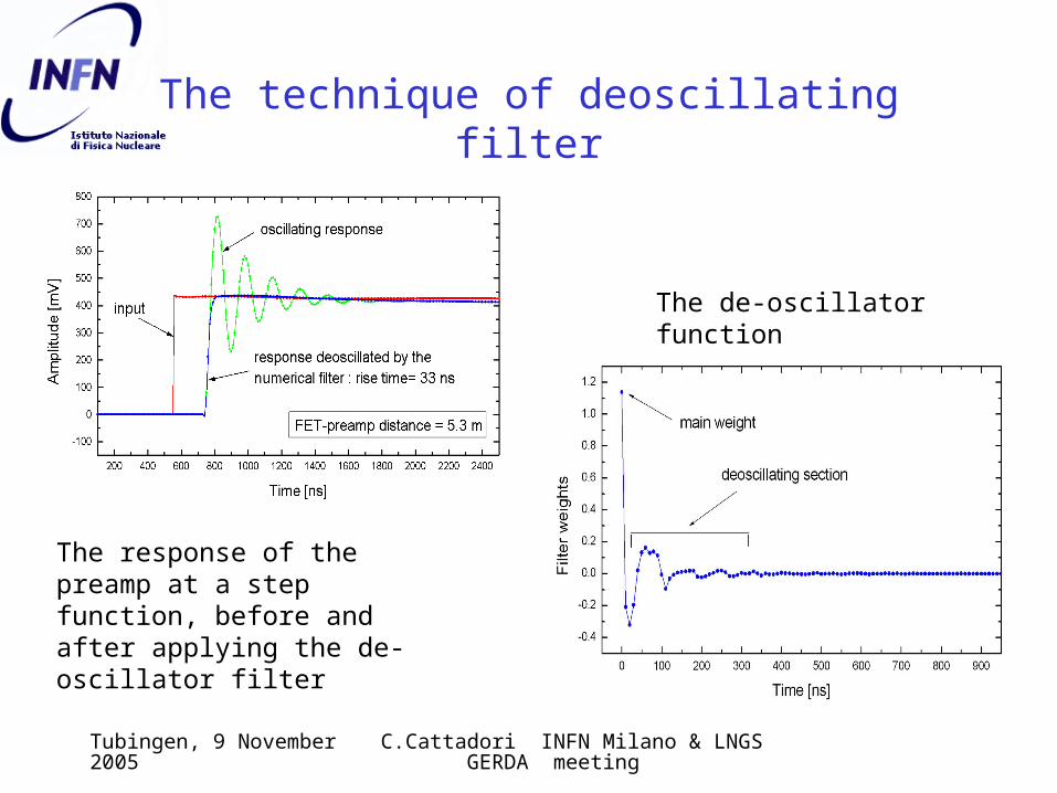
The technique of deoscillating filter
The response of the preamp at a step function, before and after applying the de-oscillator filter
The de-oscillator function
Tubingen, 9 November 2005 C.Cattadori INFN Milano & LNGS GERDA meeting
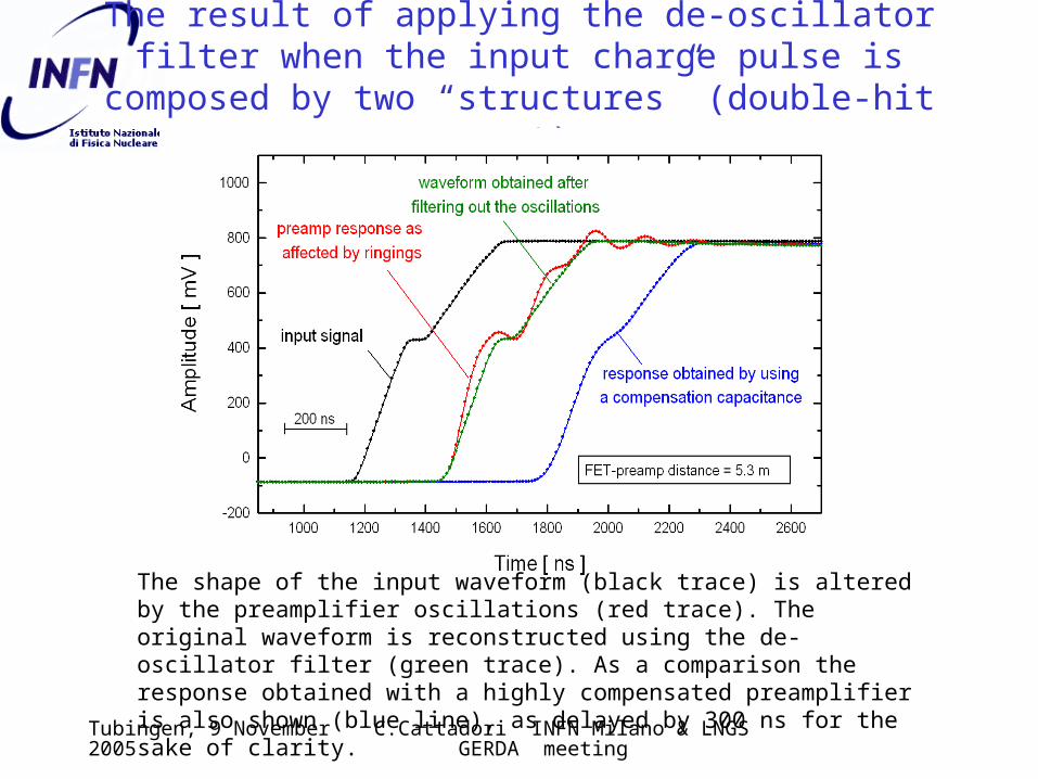
The result of applying the de-oscillator filter when the input charge pulse is composed by two
“structures” (double-hit event)
The shape of the input waveform (black trace) is altered by the preamplifier oscillations (red trace). The original waveform is reconstructed using the de-oscillator filter (green trace). As a comparison the response obtained with a highly compensated preamplifier is also shown (blue line), as delayed by 300 ns for the sake of clarity.
Tubingen, 9 November 2005 C.Cattadori INFN Milano & LNGS GERDA meeting
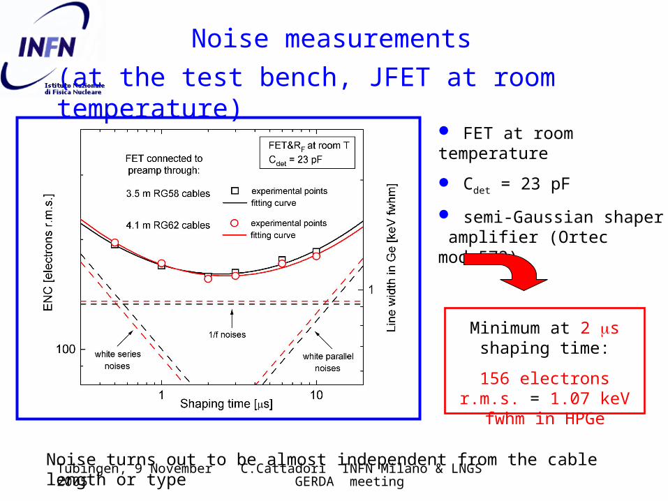
Noise measurements
FET at room temperature
Cdet = 23 pF
semi-Gaussian shaper amplifier (Ortec mod.572)
Minimum at 2 s shaping time:
156 electrons r.m.s. = 1.07 keV fwhm in
HPGe
Noise turns out to be almost independent from the cable length or type
(at the test bench, JFET at room temperature)
Tubingen, 9 November 2005 C.Cattadori INFN Milano & LNGS GERDA meeting
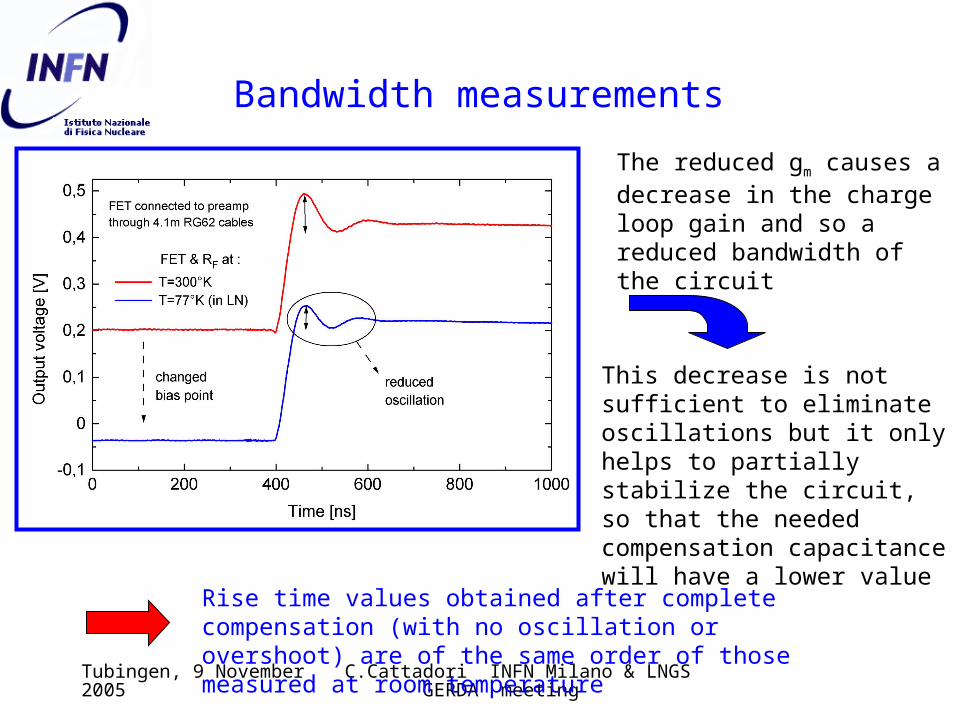
Bandwidth measurements
The reduced gm causes a decrease in the charge loop gain and so a reduced bandwidth of the circuit
This decrease is not sufficient to eliminate oscillations but it only helps to partially stabilize the circuit, so that the needed compensation capacitance will have a lower value
Rise time values obtained after complete compensation (with no oscillation or overshoot) are of the same order of those measured at room temperature
Tubingen, 9 November 2005 C.Cattadori INFN Milano & LNGS GERDA meeting
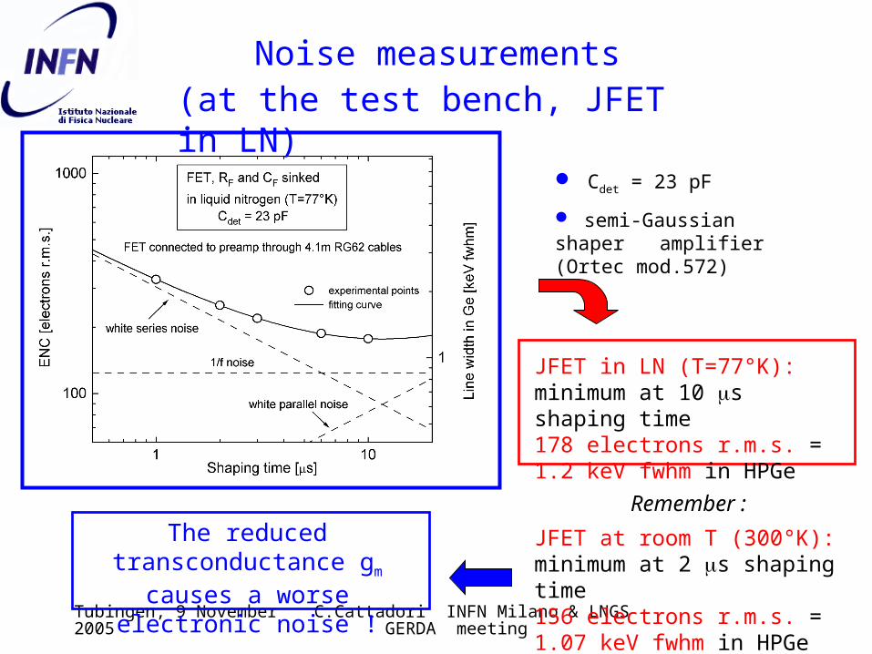
Noise measurements
Cdet = 23 pF
semi-Gaussian shaper amplifier (Ortec mod.572)
JFET at room T (300°K):minimum at 2 s shaping time156 electrons r.m.s. = 1.07 keV fwhm in HPGe
JFET in LN (T=77°K):minimum at 10 s shaping time178 electrons r.m.s. = 1.2 keV fwhm in HPGe
Remember :The reduced
transconductance gm causes a worse electronic noise !
(at the test bench, JFET in LN)
Tubingen, 9 November 2005 C.Cattadori INFN Milano & LNGS GERDA meeting
Conclusions on the use of AGATA preamps applied for GERDA
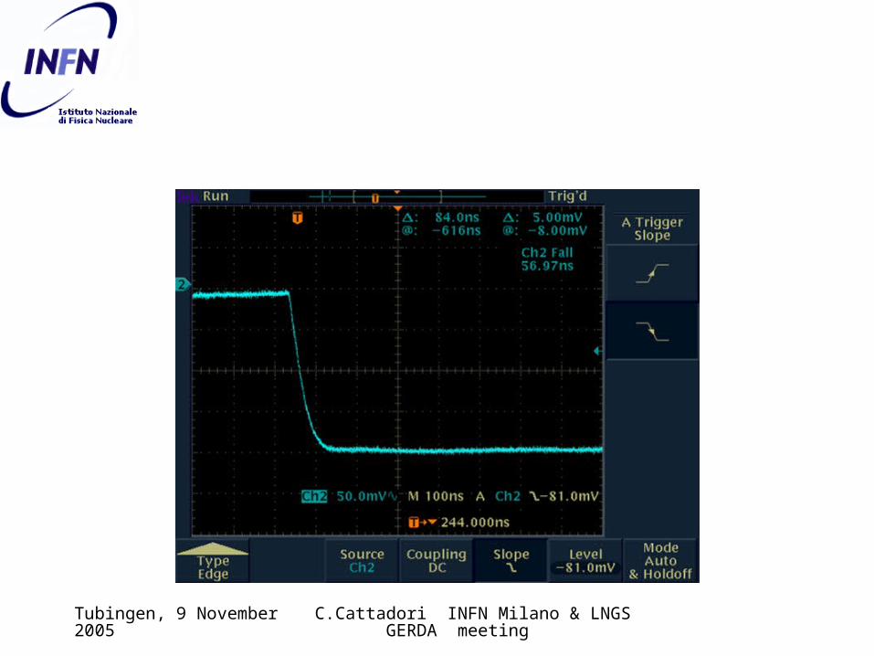
The AGATA hybrids preamps have adequate performances for GERDA but can be placed only outside the LN bath or in a vacuum insulated box inside the LN bath. In the first case they have to be connected to the front-end JFET by 2 x 6 m long cables (93 Ohms or 50 Ohms have been tested) to close the feedback loop. The delays introduced in the feedback loop by the long cables induce oscillations in the output pulse. These oscillations can be managed either compensating the capacitance in the amplifier or applying a newly developped de-oscillating technique. With the latter a rise time of the order of 33 ns has been reached with a Cdet=23 pF.

Tubingen, 9 November 2005 C.Cattadori INFN Milano & LNGS GERDA meeting
Conclusions on the use of AGATA preamps applied for GERDA
The noise of the preamplifier is 156 e- (rms) when the FET is at room temperature and 178 e- (rms) at LN temperature. This correspond respectively to 1.05 keV and 1.2 kEV FWHM in Germanium
In liquid nitrogen the JFET transconductance decreases: this fact helps to stabilize the circuit against the oscillations due to the delay lines in the charge loop BUT causes an increase in the electronic noise. The performance would improve by warming the JFET a little bit.

Tubingen, 9 November 2005 C.Cattadori INFN Milano & LNGS GERDA meeting
The monolithic N-JFET preamplifierThe monolithic N-JFET preamplifier
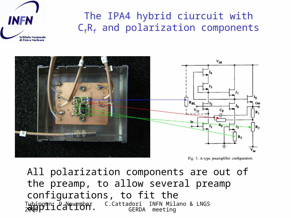
The IPA4 polarization circuit.V. Re, co-author of the IPA4 circuit, provided us several IPA4 chip in SOIC plastic case + 1 polarization board, and several useful discussions.
Shielding boxLEMO RG58
cables
Developed in the ’90s in a joint reasearch project between BNL, Italian MURST and INFN, for LAr, LKr calorimetry.

Tubingen, 9 November 2005 C.Cattadori INFN Milano & LNGS GERDA meeting
The preamps is integrated, all JFET realized with the buried-layer technology (very good noise performances in principle better than than CMOS but slow devices technology. Developped for LAr and LKr applications).
The circuital layout of the I(ntegrated)P(re)A(mplifier)4 N-JFETmonolithic preamplifier: input device J1 is dimensioned to match detectors of 10 <Cd<100 pF
Tubingen, 9 November 2005 C.Cattadori INFN Milano & LNGS GERDA meeting
The IPA4 hybrid ciurcuit with CfRf and polarization components
All polarization components are out of the preamp, to allow several preamp configurations, to fit the application.

Tubingen, 9 November 2005 C.Cattadori INFN Milano & LNGS GERDA meeting
The IPA4 N-JFET monolithic preamplifierThe IPA4 N-JFET monolithic preamplifier
Sensitivity ~ 2 -2.5 V/pC with Cf = 0.5 pF 120 mV/1 MeV in Ge
A(f) 75 dB – 60 dB (depending on the adopted configuration)
gm J1 9.7 mA/V
W,L of J1 1820 m, 15 m
Sf of J1 1.52 nV/Hz1/2
Ci 9 pFr 450 ns with Cf = 0.5 pF Output Single ended. Do not drive 50 load.Power consumption ~ 50 mWPolarity positive and NegativeV+,V- +12 V, -6 V

Tubingen, 9 November 2005 C.Cattadori INFN Milano & LNGS GERDA meeting
Published noise figure of IPA4 preamp. Never measured at LN or
LAr.
Tubingen, 9 November 2005 C.Cattadori INFN Milano & LNGS GERDA meeting
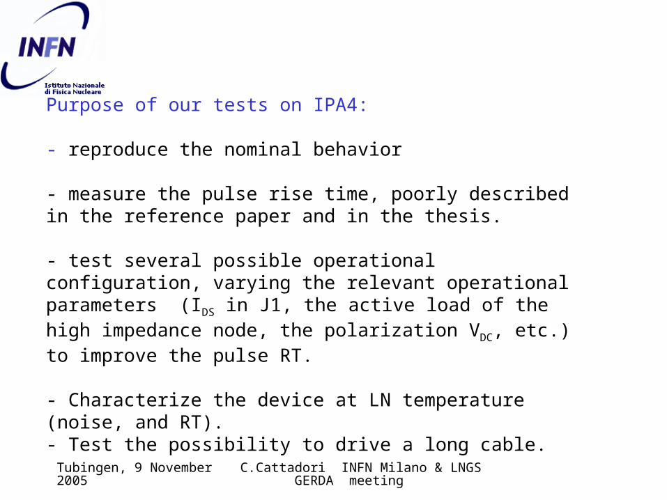
Purpose of our tests on IPA4:
- reproduce the nominal behavior
- measure the pulse rise time, poorly described in the reference paper and in the thesis.
- test several possible operational configuration, varying the relevant operational parameters (IDS in J1, the active load of the high impedance node, the polarization VDC, etc.) to improve the pulse RT.
- Characterize the device at LN temperature (noise, and RT).- Test the possibility to drive a long cable.
Tubingen, 9 November 2005 C.Cattadori INFN Milano & LNGS GERDA meeting
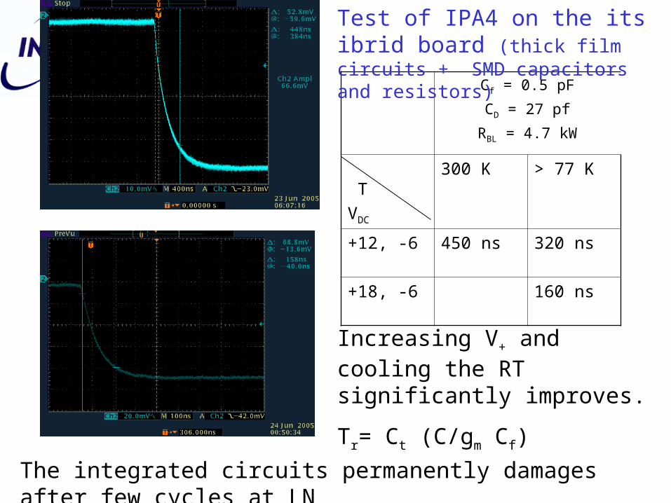
Cf = 0.5 pF
CD = 27 pf
RBL = 4.7 kW
T
VDC
300 K > 77 K
+12, -6 450 ns 320 ns
+18, -6 160 ns
Test of IPA4 on the its ibrid board (thick film circuits + SMD capacitors and resistors)
Increasing V+ and cooling the RT significantly improves.
Tr= Ct (C/gm Cf)
Measured sensitivity: 2.6 V/pCThe integrated circuits permanently damages after few cycles at LN

Tubingen, 9 November 2005 C.Cattadori INFN Milano & LNGS GERDA meeting
Test of IPA4 mounted on a newly build PCB board
• To vary safely the relevant components to vary IDSS, Cf, Cd etc, and because the thermal cycles damaged the ibrid board, we built in our lab a printed board. Performed the following tests:
• Vary RBL 4,7 k, 2,7 k, 1,8 kto increase the IDSNo significant variation of RT.
• Substitute J3 with resistor (2.5 k, 1.6 k) to reduce the active load. No significant variation of RT.
• Change CFas expected significant variation.
REMARK: All our measurements preformed with Teflon RG316 cables
Tubingen, 9 November 2005 C.Cattadori INFN Milano & LNGS GERDA meeting
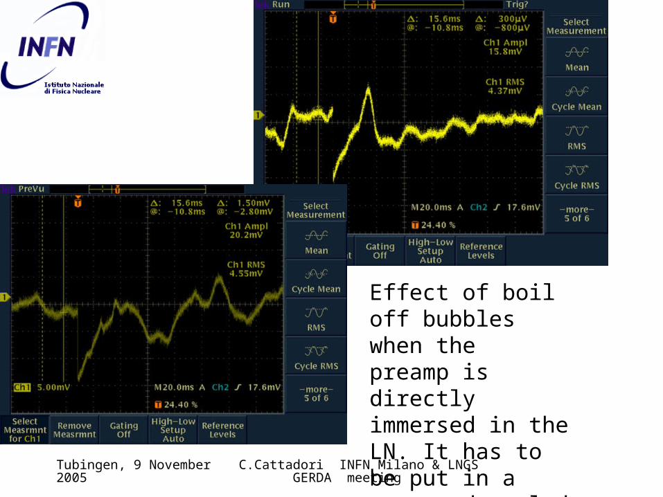
Effect of boil off bubbles when the preamp is directly immersed in the LN. It has to be put in a cage and cooled down through a cold finger.
Tubingen, 9 November 2005 C.Cattadori INFN Milano & LNGS GERDA meeting
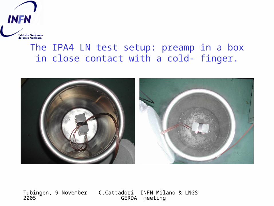
The IPA4 LN test setup: preamp in a box in close contact with a cold- finger.
Tubingen, 9 November 2005 C.Cattadori INFN Milano & LNGS GERDA meeting
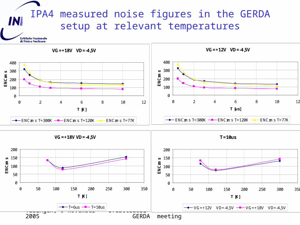
IPA4 measured noise figures in the GERDA setup at relevant temperatures
VG=+18V VD=-4,5V
0
100
200
300
400
0 2 4 6 8 10 12
T [K]
EN
Crm
s
ENCrms T=300K ENCrms T=120K ENCrms T=77K
VG=+12V VD=-4,5V
0
100
200
300
400
0 2 4 6 8 10 12
T [us]
EN
Crm
s
ENCrms T=300K ENCrms T=120K ENCrms T=77K
VG=+18V VD=-4,5V
0
50
100
150
200
0 50 100 150 200 250 300 350
T [K]
EN
Crm
s
T=6us T=10us
T=10us
0
50
100
150
200
0 50 100 150 200 250 300 350
T [K]
EN
Crm
s
VG=+12V VD=-4,5V VG=+18V VD=-4,5V
Tubingen, 9 November 2005 C.Cattadori INFN Milano & LNGS GERDA meeting
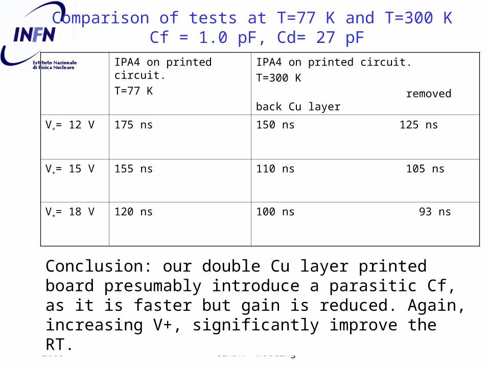
Comparison of tests at T=77 K and T=300 K Cf = 1.0 pF, Cd= 27 pF
IPA4 on printed circuit.
T=77 K
IPA4 on printed circuit.
T=300 K
removed back Cu layer
V+= 12 V 175 ns 150 ns 125 ns
V+= 15 V 155 ns 110 ns 105 ns
V+= 18 V 120 ns 100 ns 93 ns
Conclusion: our double Cu layer printed board presumably introduce a parasitic Cf, as it is faster but gain is reduced. Again, increasing V+, significantly improve the RT.

Tubingen, 9 November 2005 C.Cattadori INFN Milano & LNGS GERDA meeting
Noise measurements at T=300 KV+= 12 V,Cf=1.0 pF, Rf=10 G,Cd=27 pF
[s]
ENCrms
[e-]
0.5 300
1.0 225
2.0 185
3.0 138
6.0 115
10.0 107
[s]
ENCrms
[e-]
0.5 293
1.0 230
2.0 211
3.0 206
6.0 196
10.0 135
T=300 K T=77 K preliminar
At LN difficult to perform measurements due to microfony caused by bubbles on chip and board. Then built a rudimental cold finger, but still not perfect
Tubingen, 9 November 2005 C.Cattadori INFN Milano & LNGS GERDA meeting
Tubingen, 9 November 2005 C.Cattadori INFN Milano & LNGS GERDA meeting
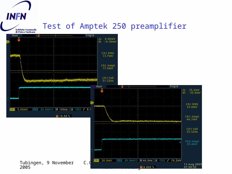
Test of Amptek 250 preamplifier
Tubingen, 9 November 2005 C.Cattadori INFN Milano & LNGS GERDA meeting
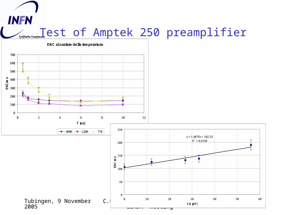
Test of Amptek 250 preamplifierENC al variare della temperatura
0
100
200
300
400
500
600
700
0 2 4 6 8 10 12
T [us]
EN
Crm
s
300K 120K 77K
y = 1,4078x + 102,35
R2 = 0,9198
0
50
100
150
200
250
0 10 20 30 40 50 60
Cd [pF]
EN
C r
ms

Tubingen, 9 November 2005 C.Cattadori INFN Milano & LNGS GERDA meeting
Comparison of the three preamps features
T[K]
Energy Sensitivity [mV/MeV (Ge)]
RT[ns]
ENCrms
[n.electrons]
Power[mW]
(AGATA+BF682)A
short cable300 150 6.5 145 ( = 2 s)
220 (AGATA+BF682)C
long cable30077
150 80 156 ( = 2 s)180 ( =10 s)
(AGATA+BF682)D
long cable77 150 33
IPA4E
300 150 (Cf = 0.5 pF) 400 (V+=12V) 110 ( =10 s)
130300 75 200 (V+=12V)
150 (V+=18V)
114 ( =10 s)
~77 75 140 (V+=12V)
60 (V+=18V)
130 ( =10 s)
~120 75 80 (V+=12V)
40 (V+=18V)
75 ( =10 s)
20AMPTEK 250 +
BF862F
300 55 27 144 ( =2 s)
77 55 55 168 ( =2 s)A CD = 27 pF, Cf = 1.5 pF 120 55 27 100B CD = 23 pF, Cf = 1.0 pF, 2x3 m cable between JFET and preamp, Ccomp=33 pFD CD = 23 pF, Cf = 1.0 pF, 2x3 m cable between JFET and preamp, no compensating capacitance.E,F CD = 27 pF, Cf = 1.0 pF

Tubingen, 9 November 2005 C.Cattadori INFN Milano & LNGS GERDA meeting
Conclusions
• Work is ongoing to look for the preamps suitable to work in our experimental conditions and a couple of solution are pursued.
• Open issue:
choice of mounting (preamp nearby cristal or in junction box), cables, gamma ray -measurements of feedback components, and of IPA4 preamplifiers in the die configuration, long term stability measurements, etc….
Tubingen, 9 November 2005 C.Cattadori INFN Milano & LNGS GERDA meeting
CMOS ASIC circuit R&D program
• Milano: AMS 0.8 m, 5 V technology
• Hd: AMS 0.6 m technology
Tubingen, 9 November 2005 C.Cattadori INFN Milano & LNGS GERDA meeting
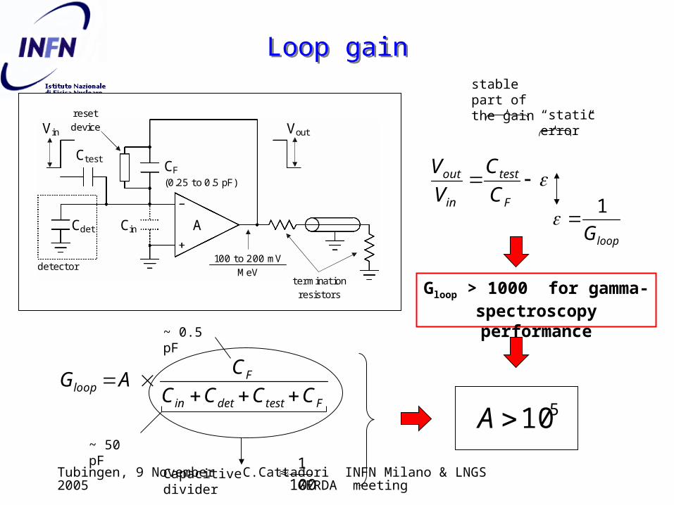
Loop gainLoop gain
F
test
in
out
C
C
V
V
loopG
1
Ftestdetin
Floop CCCC
CAG
stable part of the gain
“static error”
100
1Capacitive divider
510A~ 50 pF
~ 0.5 pF
Gloop > 1000 for gamma-spectroscopy performance
Ctest CF (0.25 to 0.5 pF)
Cin Cdet
detector
Vin Vout reset device
A
termination resistors
100 to 200 mV MeV
Tubingen, 9 November 2005 C.Cattadori INFN Milano & LNGS GERDA meeting
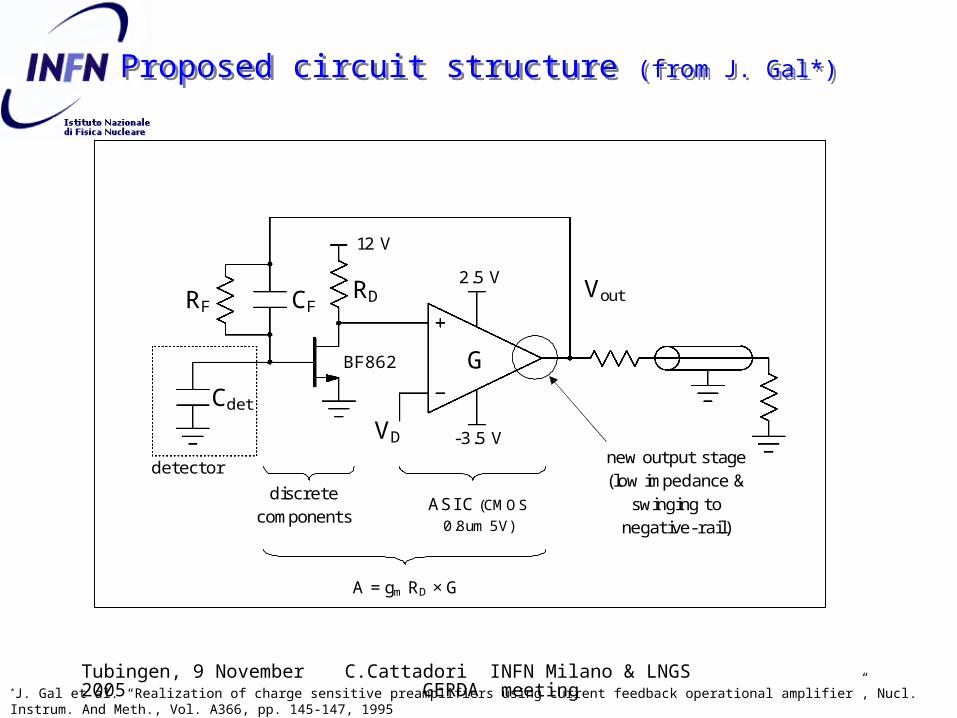
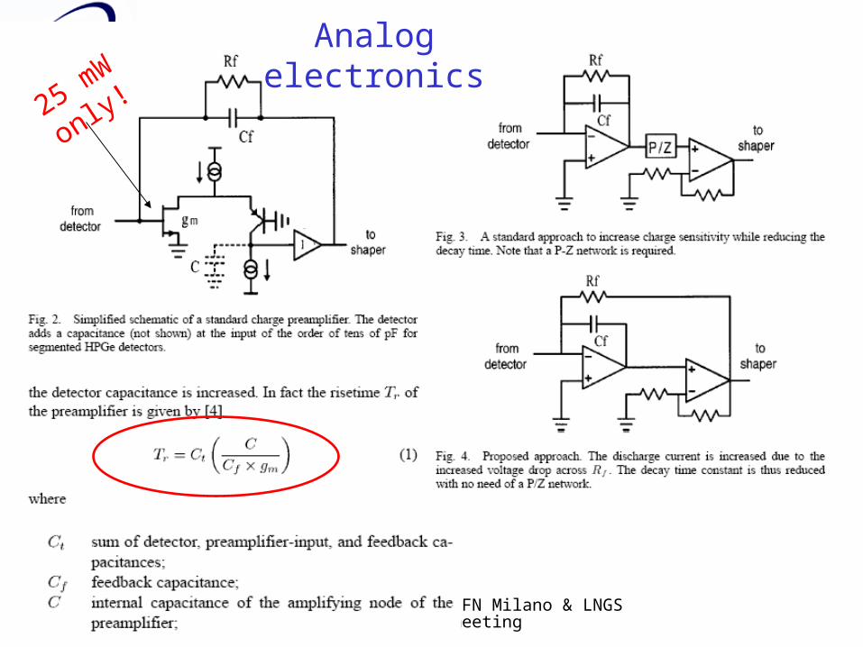
Proposed circuit structure (from J. Gal*)Proposed circuit structure (from J. Gal*)
*J. Gal et al. “Realization of charge sensitive preamplifiers using current feedback operational amplifier”, Nucl. Instrum. And Meth., Vol. A366, pp. 145-147, 1995
RD CF
BF862
Cdet
detector
Vout
G
new output stage (low impedance &
swinging to negative-rail)
RF 2.5 V
-3.5 V VD
discrete components
ASI C (CMOS 0.8um 5V)
12 V
A = gm RD × G

Tubingen, 9 November 2005 C.Cattadori INFN Milano & LNGS GERDA meeting
Spice simulation of proposed circuitSpice simulation of proposed circuit
Spice simulation
Temperature = 25 C
Cdet = 17 pF
Rise time < 10 ns with 50 Ohm cable Negative swing = -3.3V
Input referred total noise is low enough:
ENCinf = 91 el. r.m.s.
Tubingen, 9 November 2005 C.Cattadori INFN Milano & LNGS GERDA meeting
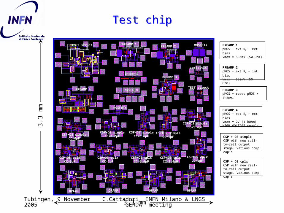
Test chipTest chip
3.3
mm
3.3 mm
MOSFETs
resistors
MOSFETs
MOSFETs
MOSFETs
PREAMP 2pMOS + ext RF + int biasVmax = 550mV (50 Ohm)
PREAMP 1pMOS + ext RF + ext biasVmax = 550mV (50 Ohm)
PREAMP 1PREAMP 2
PREAMP 3pMOS + reset pMOS + shaper
PREAMP 3
PREAMP 4
PREAMP 4pMOS + ext RF + ext biasVmax = 2V (1 kOhm)HIGH VOLTAGE comp’s
TEST struct
TEST struct
CSP+OS simple CC=0pF
CSP+OS simple CC=0.2pF
CSP+OS simple CC=0.6pF
CSP+OS simple CC=1pF
CSP+OS simple CC=1.4pF
CSP+OS cplx CC=0pF
CSP+OS cplx CC=2pF
CSP+OS cplx CC=0.4pF
CSP+OS cplx CC=1.4pF
CSP+OS cplx CC=1pF
OPAMP OPAMP OPAMP OPAMP
CSP + OS simpleCSP with new rail-to-rail output stage. Various comp cap’s
CSP + OS cplxCSP with new rail-to-rail output stage. Various comp cap’s
Tubingen, 9 November 2005 C.Cattadori INFN Milano & LNGS GERDA meeting
ConclusionConclusion
• A few issues must be addressed before a complete design of an integrated preamplifier for GERDA can be made
• The output stage must be able to drive a 6m long cable maintaining its bandwidth and a large negative voltage swing
• A test chip has been designed to address the most critical issues of this design, which will be delivered in the next months
Tubingen, 9 November 2005 C.Cattadori INFN Milano & LNGS GERDA meeting
Tubingen, 9 November 2005 C.Cattadori INFN Milano & LNGS GERDA meeting
Analog electronics
25 mW only!