tunneling characteristics of graphene characteristics of graphene . ... 14. the deforming ......
TRANSCRIPT
- 1 -
Tunneling characteristics of graphene
Young Jun Shin,1,2 Gopinadhan Kalon,1,2 Jaesung Son,1 Jae Hyun Kwon,1,2 Jing Niu,1 Charanjit S. Bhatia,1 Gengchiau Liang,1 and Hyunsoo Yang 1,2,a)
1Department of Electrical and Computer Engineering, National University of
Singapore, Singapore
2NUSNNI-NanoCore, National University of Singapore, Singapore
Negative differential conductance and tunneling characteristics of two-terminal graphene
devices are observed before and after electric breakdown, respectively. The former is
caused by the strong scattering under a high E-field, and the latter is due to the
appearance of a tunneling barrier in graphene channel induced by a structural
transformation from crystalline graphene to disordered graphene because of the
breakdown. Using Raman spectroscopy and imaging, the presence of non-uniform
disordered graphene is confirmed. A memory switching effect of 100000% ON/OFF ratio
is demonstrated in the tunneling regime which can be employed in various applications.
a) e-mail address: [email protected]

- 2 -
Graphene, a single layer of carbon atoms, has attracted tremendous attention in the
last few years due to its potential applications in the area of ultrafast devices.1, 2 The
successful demonstration of 100 GHz graphene transistor and the success of various
methods to produce large scale graphene are indicating that graphene can be a promising
material in the post-silicon era.3, 4 Although graphene has superior physical properties such
as very high mobility (Fermi velocity vF~106 m/s), a low ON/OFF ratio due to its
semi-metallic property prevents graphene from being engineered as logic and memory
devices. Two-terminal devices coupled with a nonlinear current-voltage (I-V)
characteristic can be a solution to overcome this shortcoming.5-7
In this Letter, the tunneling behavior in graphene at a high bias voltage is reported. A
high voltage bias is applied across the electrodes to induce a breakdown in the graphene
channel. Negative differential conductance is found just before the breakdown as a
symptom of the tunneling behavior. Understanding the behavior of carrier transport in
graphene under a high bias voltage is important since graphene holds promising future as
various components including interconnects because of its high current carrying capacity.
After the breakdown, non-linear I-V curves, which have the same characteristic as
tunneling diodes, are measured. Graphene is examined by Raman spectroscopy and it
appears that crystal graphene is transformed into non-uniform disordered graphene under
the application of high bias. Reproducible tunneling behavior and current hysteresis with a
100000% ON/OFF ratio are observed after the breakdown. The tunneling effect can be
attributed to a non-uniform disordered system which introduces energy barriers in the
graphene channel. To confirm this further, glassy carbon is uniformly deposited by pulsed
laser deposition (PLD) and is subjected to the similar high bias voltage. The linear I-V

- 3 -
characteristics of glassy carbon under a high bias condition indicate that the tunneling
diode effect is a unique property of non-uniform disordered graphene.
Mechanical exfoliation is used to prepare single and multi-layer graphene.8
Mechanically cleaved graphene is transferred to a highly p-doped Si substrate covered by
a 300nm thick SiO2 layer. Number of layers and quality of graphene is determined by
Raman spectroscopy. Further details on the sample preparation and identification can be
found in our earlier work.9 Electrodes are patterned by standard lithography and Cr/Au (5
nm/80 nm) is deposited by a thermal evaporator. The contact deposition is followed by
standard lift-off procedures. The I-V measurements with a two-probe configuration are
carried out with a closed cycle helium cryostat under a base pressure of less than 1 × 10⁻⁸
Torr at 3.8 K.
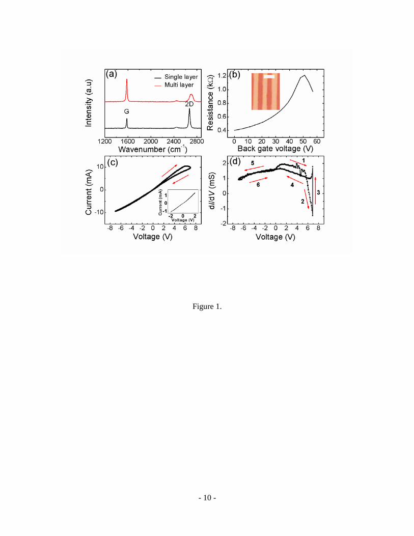
Single and multi-layer graphene samples are identified by Raman spectra as shown in
Fig. 1(a) and the transport data from single layer graphene are reported in this work.
In-plane vibrational G band (1580 cm-1) and two-phonon 2D band (2670 cm-1) are clearly
visible without any indication of disorder D band peak and the number of layers of the
graphene sample is determined by estimating the width of 2D peak.10 Figure 1(b) shows
the two-terminal resistance as a function of back gate voltage. From the shift of the Dirac
point to the positive side of the applied back gate voltage, graphene is identified to be hole
dominant. The Dirac point is shifted due to unintentional doping such as the adsorption of
water molecules making graphene p-type.8 The inset of Fig. 1(b) shows the optical image
of a graphene device on top of a Si wafer with 300nm thick SiO2 after the Cr/Au electrode
deposition. The inset of Fig. 1(c) shows the typical linear I-V curve with the low bias
voltage less than 2 V in graphene devices. As shown in Fig. 1(c), the I-V curve is linear at a

- 4 -
low bias voltage, but becomes non-linear and slightly hysteretic at a higher bias.11 Also the
current starts to decrease as the applied voltage is continuously increased above 6 V. When
the current reaches a maximum (dI/dV = 0), the current density is ~1.9×10⁸ A/cm2 with a
sample width of 16 µm and a thickness of 0.35 nm. When the I-V curve is numerically
differentiated, we can clearly identify a negative differential conductance behavior as
shown in Fig. 1(d). This negative differential conductance might be attributed to the
self-heating effects caused by strong electron scattering due to hot non-equilibrium optical
phonons similar to what is observed in carbon nanotubes.12
After the observation of negative differential conductance, the sweep voltage is
increased further to induce a breakdown in graphene channel as was reported recently that
graphene nanoribbons exhibit a breakdown current density, on the order of 108 A/cm2.13 As
can be seen in Fig. 2(a), the voltage sweep is halted as soon as the breakdown occurs.
Figure 2(b) shows non-linear I-V behavior of graphene devices instead of linear increase in
current with increasing the bias voltage, when graphene undergoes the breakdown. It can
be clearly seen in the logarithmic scale that current starts increasing drastically when the
bias exceed the threshold voltage of 7 V as shown in Fig. 2(c). After the measurement,
graphene is examined by Raman spectroscopy and we find out that crystalline graphene is
converted to disordered graphene. Interestingly, this disordered system is very different
from typical disordered graphene created by an oxygen plasma treatment. Compared to the
typical disordered system, the transformed graphene by an electrical breakdown has mixed
phases such as amorphous-like (the upper inset of Fig. 2(a)) and graphene-like (the lower
inset of Fig. 2(a)) phases. From the investigation by Raman spectroscopy, the breakdown
can be considered as a “deforming process”, which is the opposite concept of the forming
- 5 -
process, the change in the spatial distribution of oxygen ions by applying the bias voltage,
in the oxide resistance switching devices.14 The deforming process introduces randomly
distributed energy barriers caused by amorphous-like phase in the graphene channel.
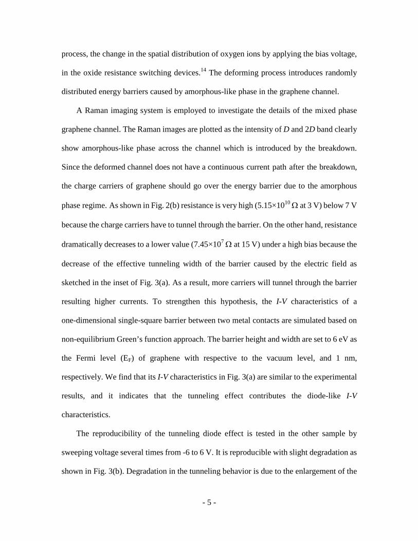
A Raman imaging system is employed to investigate the details of the mixed phase
graphene channel. The Raman images are plotted as the intensity of D and 2D band clearly
show amorphous-like phase across the channel which is introduced by the breakdown.
Since the deformed channel does not have a continuous current path after the breakdown,
the charge carriers of graphene should go over the energy barrier due to the amorphous
phase regime. As shown in Fig. 2(b) resistance is very high (5.15×10¹⁰ Ω at 3 V) below 7 V
because the charge carriers have to tunnel through the barrier. On the other hand, resistance
dramatically decreases to a lower value (7.45×10⁷ Ω at 15 V) under a high bias because the
decrease of the effective tunneling width of the barrier caused by the electric field as
sketched in the inset of Fig. 3(a). As a result, more carriers will tunnel through the barrier
resulting higher currents. To strengthen this hypothesis, the I-V characteristics of a
one-dimensional single-square barrier between two metal contacts are simulated based on
non-equilibrium Green’s function approach. The barrier height and width are set to 6 eV as
the Fermi level (EF) of graphene with respective to the vacuum level, and 1 nm,
respectively. We find that its I-V characteristics in Fig. 3(a) are similar to the experimental
results, and it indicates that the tunneling effect contributes the diode-like I-V
characteristics.
The reproducibility of the tunneling diode effect is tested in the other sample by
sweeping voltage several times from -6 to 6 V. It is reproducible with slight degradation as
shown in Fig. 3(b). Degradation in the tunneling behavior is due to the enlargement of the

- 6 -
barrier width caused by Joule heating. More than 20 devices are tested and it turns out that
each device has a different threshold voltage since the breakdown is a random process.
When the bias voltage is swept for even higher bias in the tunneling regime, current
hysteresis is observed as plotted in Fig. 3(c). The range of the ON/OFF ratio is from 1000%
to 100000%. Current hysteresis is repeatable but degraded gradually. To understand better
and engineer the current hysteresis from the mixed phase channel, further studies are
required.
In order to verify the unique nature of disordered graphene by the breakdown, we
further study the I-V characteristics from other carbon thin films. For this a 2 nm thick
glassy carbon film is deposited by pulsed laser deposition and tested in the same
measurement conditions. From the inset of Fig. 3(d), the structure of deposited glassy
carbon, strong D peak and weak 2D peak in Raman spectra, is similar to the structure of
graphene after the breakdown. However, a complete mapping by Raman spectroscopy
reveals that the glassy structure is very uniform unlike to the disordered graphene by the
breakdown. When a high bias is applied across the glassy carbon channel, linear I-V
characteristics are observed in Fig. 3(d), which demonstrates that the tunneling
characteristic is a unique property of non-uniform disordered graphene. If the tunneling
behavior in resistance of Fig. 2(b) is caused by electrical annealing, it should not be
reversible and reproducible.15 Non-linear I-V characteristics of graphene and carbon
nanotubes due to a mechanical discontinuity have been reported.5, 16, 17 We carefully check
all our devices by scanning electron microscopy after the breakdown, but any mechanical
discontinuity is not found as can be seen in the inset of Fig. 2(c).

- 7 -
In conclusion, we report the tunneling characteristic of graphene from the
two-terminal devices after the breakdown. Negative differential conductance is also
observed when a high voltage bias is applied across the graphene channel. The tunneling
behavior could be attributed to the formation of non-uniform disordered graphene, which
is created by the breakdown. We propose that the non-uniform disordered structure can
introduce energy barriers in the graphene channel. This hypothesis is supported by the
Raman images and the simulated results of the I-V characteristics from a one-dimensional
single-square barrier. A 2 nm thick glassy carbon film, which is uniformly disordered, is
compared and linear I-V characteristics of grassy carbon prove that the tunneling
characteristic is a unique property of non-uniform disordered graphene. The observed
memory switching effect up to a 100000% ON/OFF ratio may open up new possibilities
for various graphene based applications and the tunneling effect paves a way to study
graphene disordered characteristics such as defect magnetism or a weak localization in
graphene.18
This work was supported by the Singapore Ministry of Education Academic
Research Fund Tier 2 (MOE2008-T2-1-105).
- 8 -
References 1 A. K. Geim, Science 324, 1530 (2009). 2 A. K. Geim and K. S. Novoselov, Nat. Mater. 6, 183 (2007). 3 Y. M. Lin, C. Dimitrakopoulos, K. A. Jenkins, D. B. Farmer, H. Y. Chiu, A. Grill, and P.
Avouris, Science 327, 662 (2010). 4 S. Bae, H. Kim, Y. Lee, X. Xu, J.-S. Park, Y. Zheng, J. Balakrishnan, T. Lei, H. Ri Kim,
Y. I. Song, Y.-J. Kim, K. S. Kim, B. Ozyilmaz, J.-H. Ahn, B. H. Hong, and S. Iijima, Nat. Nanotechnol. 5, 574 (2010).
5 B. Standley, W. Bao, H. Zhang, J. Bruck, C. N. Lau, and M. Bockrath, Nano Lett. 8, 3345 (2008).
6 I. Meric, M. Y. Han, A. F. Young, B. Ozyilmaz, P. Kim, and K. L. Shepard, Nat. Nanotechnol. 3, 654 (2008).
7 J. Yao, Z. Jin, L. Zhong, D. Natelson, and J. M. Tour, ACS Nano 3, 4122 (2009). 8 K. S. Novoselov, A. K. Geim, S. V. Morozov, D. Jiang, Y. Zhang, S. V. Dubonos, I. V.
Grigorieva, and A. A. Firsov, Science 306, 666 (2004). 9 Y. J. Shin, Y. Wang, H. Huang, G. Kalon, A. T. S. Wee, Z. Shen, C. S. Bhatia, and H.
Yang, Langmuir 26, 3798 (2010). 10 A. C. Ferrari, J. C. Meyer, V. Scardaci, C. Casiraghi, M. Lazzeri, F. Mauri, S. Piscanec,
D. Jiang, K. S. Novoselov, S. Roth, and A. K. Geim, Phys. Rev. Lett. 97, 187401 (2006). 11 A. Barreiro, M. Lazzeri, J. Moser, F. Mauri, and A. Bachtold, Phys. Rev. Lett. 103,
076601 (2009). 12 E. Pop, D. Mann, J. Cao, Q. Wang, K. Goodson, and H. Dai, Phys. Rev. Lett. 95, 155505
(2005). 13 R. Murali, Y. Yang, K. Brenner, T. Beck, and J. D. Meindl, Appl. Phys. Lett. 94, 243114
(2009). 14 R. Waser and M. Aono, Nat. Mater. 6, 833 (2007). 15 H. L. Wang, X. R. Wang, X. L. Li, and H. J. Dai, Nano Res. 2, 336 (2009). 16 Y. Li, A. Sinitskii, and J. M. Tour, Nat. Mater. 7, 966 (2008). 17 P. G. Collins, M. Hersam, M. Arnold, R. Martel, and P. Avouris, Phys. Rev. Lett. 86,
3128 (2001). 18 O. V. Yazyev, Phys. Rev. Lett. 101, 037203 (2008).
- 9 -
Figure Captions
Figure 1. (a) Raman spectra of single layer and multi-layer graphene. (b) Resistance vs.
back gate voltage of a graphene sample. The inset in (b) shows the optical image
of graphene with gold contacts (the scale bar is 8 µm). (c) I-V curve in the high
bias range. The inset in (c) shows I-V curve in the low bias range. (d)
Differential conductance versus bias voltage.
Figure 2. (a) I-V curve through an electrical breakdown. The insets in (a) show different
Raman spectra measured at two different locations in the graphene channel
after the breakdown. (b) I-V curve after breakdown. (c) Absolute value of
current as a function of bias voltage in a logarithmic scale. The inset in (c)
shows a scanning electron microscopy image of the graphene channel after the
breakdown (the scale bar is 1 µm). (d) Optical image of the sample (top panel)
and Raman images plotted by the intensity of D and 2D band (the scale bar is 4
µm). The dotted red line indicates the area of Raman imaging. The blue arrows
show the direction of current flow through the graphene channel.
Figure 3. (a) Simulated I-V data. The insets show the energy diagrams of disordered
graphene system without and with the bias voltage. (b) Repeated I-V curves
after the breakdown. (c) I-V curve in the high bias range after the breakdown.
The inset in (c) shows I-V curve in a low bias range after the breakdown. (d)
I-V curve of a glassy carbon film. The inset in (d) shows the Raman spectra of
glassy carbon.
- 10 -
Figure 1.

- 11 -
Figure 2.

- 12 -
Figure 3.