tusb522p datasheet - ti.com · os2 4 i, cmos sets the output swing (differential voltage amplitude)...
TRANSCRIPT

20"
RedriverUSB HostUSB
Connector
20" 1"-6"
Main PCB
Main PCB
RedriverUSB Host Device
Device PCBConnector
3m USB3.0 Cable
Receiver/Equalizer
Driver
EQCNTRL
LFPSCONTROLLER
DEMPCNTRL
DriverReceiver/Equalizer
Dua
lT
erm
inat
ion
Dua
lT
erm
inat
ion
DetectOS
Cntrl.
Detect
Dua
lT
erm
inat
ion
Dua
lT
erm
inat
ion
EN_RXD
CHANNEL 1
CHANNEL 2
RX1P
RX1N
EQ1
EQ2
DE1
DE2
TX1P
TX1N
RX2P
RX2N
TX2N
TX2N
OS1 OS2
Copyright © 2016, Texas Instruments Incorporated
Product
Folder
Order
Now
Technical
Documents
Tools &
Software
Support &Community
An IMPORTANT NOTICE at the end of this data sheet addresses availability, warranty, changes, use in safety-critical applications,intellectual property matters and other important disclaimers. PRODUCTION DATA.
TUSB522PSLLSEV9B –JULY 2016–REVISED NOVEMBER 2017
TUSB522P 3.3 V Dual-Channel USB 3.1 GEN 1 Redriver, Equalizer
1
1 Features1• USB3.1 GEN1 5 Gbps, Dual-Channel Re-Driver
with 3.3-V Power Supply• Ultra-Low-Power Architecture
– Active: 98 mA– U2, U3: 1.2 mA– Disconnect 265 µA– Shutdown 60 µA
• Optimal Receiver Equalization– of 3, 6, 9 dB at 2.5 GHz
• Output Driver De-emphasis of 0, 3.5, and 6 dB• Automatic LFPS De-Emphasis Control to Meet
USB 3.1 Certification Requirements• No Host/Device-Side Requirement• Hot-Plug Capable• Industrial Temperature Range: –40ºC to 85ºC
TUSB522PI• Commercial Temperature Range: 0ºC to 70ºC
TUSB522P
2 Applications• Cell Phones• Tablets• Notebooks• Desktops• Docking Stations• Backplanes and Active Cables
3 DescriptionThe TUSB522P is a fourth generation, dual-channel,single-lane USB 3.1 GEN1 redriver and signalconditioner supporting 5 Gbps. The device offers lowpower consumption on a 3.3 V supply with its ultra-low-power architecture. The redriver also supportsthe USB 3.1 low power modes, which further reducesidle power consumption.
The dual-channel capability enables the system tomaintain signal integrity on both transmit and receivedata paths. The receiver equalization has three gainsettings to overcome channel degradation frominsertion loss and inter-symbol interference. Thesesettings are controlled from the EQ pins. Tocompensate for transmission line losses, the outputdriver supports configuration of De-Emphasis withpins DE. Additionally, automatic LFPS De-Emphasiscontrol allows for full USB 3.1 compliance. Thesesettings allow optimal performance, increasedsignaling distance, and flexibility in placement of theTUSB522P in theUSB 3.1 GEN1 path.
Device Information(1)
PART NUMBER PACKAGE BODY SIZE (NOM)TUSB522P
VQFN (24) 4.00 mm x 4.00 mmTUSB522PI
(1) For all available packages, see the orderable addendum atthe end of the data sheet.
SPACER
Simplified Schematic
2
TUSB522PSLLSEV9B –JULY 2016–REVISED NOVEMBER 2017 www.ti.com
Product Folder Links: TUSB522P
Submit Documentation Feedback Copyright © 2016–2017, Texas Instruments Incorporated
Table of Contents1 Features .................................................................. 12 Applications ........................................................... 13 Description ............................................................. 14 Revision History..................................................... 25 Pin Configuration and Functions ......................... 36 Specifications......................................................... 4
6.1 Absolute Maximum Ratings ...................................... 46.2 ESD Ratings.............................................................. 46.3 Recommended Operating Conditions....................... 46.4 Thermal Information .................................................. 56.5 Electrical Characteristics, Power Supply .................. 56.6 Electrical Characteristics, DC ................................... 56.7 Electrical Characteristics, AC.................................... 6
7 Detailed Description .............................................. 87.1 Overview ................................................................... 87.2 Functional Block Diagram ......................................... 87.3 Feature Description................................................... 9
7.4 Device Functional Modes........................................ 108 Application and Implementation ........................ 11
8.1 Application Information............................................ 118.2 Typical Application ................................................. 11
9 Power Supply Recommendations ...................... 1310 Layout................................................................... 14
10.1 Layout Guidelines ................................................. 1410.2 Layout Example .................................................... 14
11 Device and Documentation Support ................. 1511.1 Documentation Support ....................................... 1511.2 Related Links ........................................................ 1511.3 Receiving Notification of Documentation Updates 1511.4 Community Resources.......................................... 1511.5 Trademarks ........................................................... 1511.6 Electrostatic Discharge Caution............................ 1511.7 Glossary ................................................................ 15
12 Mechanical, Packaging, and OrderableInformation ........................................................... 15
4 Revision History
Changes from Revision A (October 2016) to Revision B Page
• Changed the values in the FOR OS = HIGH column of Table 1 ......................................................................................... 10
Changes from Original (July 2016) to Revision A Page
• Changed the device From Preview To: Production................................................................................................................ 1

6 5 4 3 2 1
13 14 15 16 17 18
19
20
21
22
23
24
12
11
10
9
8
7
CH1
CH2
PAD
(must be soldered to GND)
VCCOS2 DE2 EQ1EN_RXDNC
NC
RX1N
RX1P
TX2N
GND
TX2P
VCC NC
GND
TX1N
TX1P
RX2N
RX2P
NC
OS1 DE1 EQ2RSV
3
TUSB522Pwww.ti.com SLLSEV9B –JULY 2016–REVISED NOVEMBER 2017
Product Folder Links: TUSB522P
Submit Documentation FeedbackCopyright © 2016–2017, Texas Instruments Incorporated
5 Pin Configuration and Functions
RGE Package24-Pin (VQFN)
Top View
Pin FunctionsPIN
I/O DESCRIPTIONNAME NO.RX1N 8 Differential I Differential input for 5 Gbps negative signal on Channel 1RX1P 9 Differential I Differential input for 5 Gbps positive signal on Channel 1TX1N 23 Differential O Differential output for 5 Gbps negative signal on Channel 1TX1P 22 Differential O Differential output for 5 Gbps positive signal on Channel 1RX2N 20 Differential I Differential input for 5 Gbps negative signal on Channel 2RX2P 19 Differential I Differential input for 5 Gbps positive signal on Channel 2TX2N 11 Differential O Differential output for 5 Gbps negative signal on Channel 2TX2P 12 Differential O Differential output for 5 Gbps positive signal on Channel 2
EQ1 2 I, CMOS
Sets the receiver equalizer gain for Channel 1. 3-state input with integrated pull-up and pull-down resistors.EQ1 = Low = 3 dBEQ1 = Mid = 6 dBEQ1 = High = 9 dB
DE1 16 I, CMOS
Sets the output de-emphasis for Channel 1. 3-state input with integrated pull-up and pull-down resistors.DE1 = Low = 0 dBDE1 = Mid = -3.5 dBDE1 = High = -6.2 dBNote: When OS = Low
OS1 15 I, CMOS
Sets the output swing (differential voltage amplitude) for Channel 1. 2-state input with anintegrated pull down resistor.OS1 = Low = 0.9 mVOS1 = High = 1.1 mV
EQ2 17 I, CMOS
Sets the receiver equalizer gain for Channel 2. 3-state input with integrated pull-up and pull-down resistors.EQ2 = Low = 3 dBEQ2 = Mid = 6 dBEQ2 = High = 9 dB

4
TUSB522PSLLSEV9B –JULY 2016–REVISED NOVEMBER 2017 www.ti.com
Product Folder Links: TUSB522P
Submit Documentation Feedback Copyright © 2016–2017, Texas Instruments Incorporated
Pin Functions (continued)PIN
I/O DESCRIPTIONNAME NO.
DE2 3 I, CMOS
Sets the output de-emphasis for Channel 2. 3-state input with integrated pull-up and pull-down resistors.DE2 = Low = 0 dBDE2 = Mid = -3.5 dBDE2 = High = -6.2 dBNote: When OS = Low
OS2 4 I, CMOS
Sets the output swing (differential voltage amplitude) for Channel 2. 2-state input with anintegrated pull down resistor.OS2 = Low = 0.9 mVOS2 = High = 1.1 mV
EN_RXD 5 I, CMOSEnable. The device has a 660-kΩ pulldown resistor. Device is active when EN_RXD = High.Drive actively high or install a pullup resistor (recommend 4.7 KΩ) for normal operation. Doesreset state machine.
RSV 14 I, CMOS Reserved. Can be left as No-connect.VCC 1, 13 P Positive Power Supply. Power Supply is 3.3 V.
GND 10, 21, PAD G Ground. PAD must be connected to Ground. Pins 10, 21 can be connected to Ground or leftunconnected.
NC 6, 7, 18, 24 No Connection. These pins can be tied to any desired voltages including connecting them toGND.
(1) Stresses beyond those listed under Absolute Maximum Ratings may cause permanent damage to the device. These are stress ratingsonly, which do not imply functional operation of the device at these or any other conditions beyond those indicated under RecommendedOperating Conditions. Exposure to absolute-maximum-rated conditions for extended periods may affect device reliability.
(2) All voltage values are with respect to the GND terminals.
6 Specifications
6.1 Absolute Maximum Ratingsover operating free-air temperature range (unless otherwise noted) (1)
MIN MAX UNITSupply Voltage Range (2) VCC –0.5 4 V
Voltage Range at any input or output terminalDifferential I/O –0.5 1.5 VCMOS Inputs –0.5 4 V
Junction temperature, TJ 105 °CStorage temperature, Tstg –65 150 °C
(1) JEDEC document JEP155 states that 500-V HBM allows safe manufacturing with a standard ESD control process.(2) JEDEC document JEP157 states that 250-V CDM allows safe manufacturing with a standard ESD control process.
6.2 ESD RatingsVALUE UNIT
V(ESD) Electrostatic dischargeHuman-body model (HBM), per ANSI/ESDA/JEDEC JS-001 (1) ±2000
VCharged-device model (CDM), per JEDEC specification JESD22-C101 (2) ±500
6.3 Recommended Operating Conditionsover operating free-air temperature range (unless otherwise noted)
MIN NOM MAX UNIT
VCCMain power supply 3 3.3 3.6 VSupply Ramp Requirement 100 ms
V(PSN) Supply Noise on VCC Terminals 100 mV
TA Operating free-air temperatureTUSB522P 0 70 °CTUSB522PI –40 85 °C
C(AC) AC coupling capacitor 75 100 200 nF

5
TUSB522Pwww.ti.com SLLSEV9B –JULY 2016–REVISED NOVEMBER 2017
Product Folder Links: TUSB522P
Submit Documentation FeedbackCopyright © 2016–2017, Texas Instruments Incorporated
(1) For more information about traditional and new thermal metrics, see the Semiconductor and IC Package Thermal Metrics applicationreport.
6.4 Thermal Information
THERMAL METRIC (1)TUSB522P
UNITRGE (VQFN)24 PINS
RθJA Junction-to-ambient thermal resistance 51.2 °C/WRθJC(top) Junction-to-case (top) thermal resistance 55.9 °C/WRθJB Junction-to-board thermal resistance 28.3 °C/WψJT Junction-to-top characterization parameter 2.0 °C/WψJB Junction-to-board characterization parameter 28.3 °C/WRθJC(bot) Junction-to-case (bottom) thermal resistance 9.7 °C/W
6.5 Electrical Characteristics, Power Supplyover operating free-air temperature range (unless otherwise noted)
PARAMETER TEST CONDITIONS MIN TYP MAX UNIT
ICC(ACTIVE) Average active current
Link in U0 with GEN1 data transmission.RSV, EQ cntrl pins = NC, EN_RXD = VCC,k28.5 pattern at 5 Gbps,VID = 1000 mVpp, OS = 900 mV and DE =3.5 dB
98 mA
ICC(U2U3) Average current in U2/U3 Link in U2 or U3 1.2 mA
ICC(NC) Average current disconnect mode Link in Disconnect mode 265 µA
ICC(SHUTDOWN) Average shutdown current EN_RXD = L 60 µA
6.6 Electrical Characteristics, DCover operating free-air temperature range (unless otherwise noted)
PARAMETER TEST CONDITIONS MIN TYP MAX UNIT
3-State CMOS Inputs(EQ1/2, DE1/2)
VIH High-level input voltage VCC x 0.8 V
VIM Mid-level input voltage VCC / 2. V
VIL Low-level input voltage VCC x 0.2 V
VF Floating voltage VIN = High impedance 0.36 x VCC V
RPU Internal pull-up resistance 410 kΩ
RPD Internal pull-down resistance 240 kΩ
IIH High-level input current VIN = 3.6 V 26 µA
IIL Low-level input current VIN = GND, VCC = 3.6.V –26 µA
2-State CMOS Input (OS1/2, EN_RXD)
VIH High-level input voltage VCC x 0.7 V
VIL Low-level input voltage VCC x 0.3 V
RPD Internal pull-down resistance 660 kΩ
IIH Low-level input current VIN = 3.6 V 25 µA
IIL Low-level input current VIN = GND, VCC = 3.6.V –10 µA

6
TUSB522PSLLSEV9B –JULY 2016–REVISED NOVEMBER 2017 www.ti.com
Product Folder Links: TUSB522P
Submit Documentation Feedback Copyright © 2016–2017, Texas Instruments Incorporated
6.7 Electrical Characteristics, ACover operating free-air temperature range (unless otherwise noted)
PARAMETER TEST CONDITIONS MIN TYP MAX UNIT
Differential Receiver (RXP, RXN)
V(RX-DIFF-PP)
Input differential voltage swing.AC-coupled differential peak-to-peaksignal measured post CTLE through areference channel
100 1200 mVpp
V(RX-DC-CM)Common-mode voltage bias in thereceiver (DC) 0.7 V
R(RX-DIFF-DC) Differential input impedance (DC)Present after a GEN1 device isdetected on TXP/TXN
72 120 Ω
R(RX-CM-DC)Receiver DC Common Modeimpedance 18 30 Ω
Z(RX-HIGH-IMP-DC-POS) Common-mode input impedance withtermination disabled (DC)
Present when no GEN1 device isdetected on TXP/TXN. Measured overthe range of 0-500 mV with respect toGND.
25 kΩ
V(RX-SIGNAL-DET-DIFF-PP)Input Differential peak-to-peak SignalDetect Assert Level At 5 Gbps, no input channel loss clock
pattern
85 mV
V(RX-IDLE-DET-DIFF-PP)Input Differential peak-to-peak SignalDetect De-assert Level 85 mV
V(RX-LFPS-DET-DIFF-PP)Low Frequency Periodic Signaling(LFPS) Detect Threshold Below the minimum is squelched. 100 300 mV
V(RX-CM-AC-P) Peak RX AC common mode voltage Measured at package pin 150 mV
V(detect) Voltage change to allow receiver detect Positive voltage to sense receivertermination 600 mV
C(RX-PARASITIC) Voltage change to allow receiver detect At 2.5 GHz 0.17 0.63 0.99 pF
RL(RX-DIFF) Differential Return Loss50 MHz – 1.25 GHz at 90 Ω –19 dB
2.5 GHz at 90 Ω –14 dB
RL(RX-CM) Common Mode Return Loss 50 MHz – 1.25 GHz at 90 Ω –13 dB
Differential Transmitter (TXP, TXN)
V(TX-DIFF-PP)Transmitter differential voltage swing(transition-bit)
OS Low, 0dB DE 0.8 0.9 Vpp
OS High, 0dB DE 1.1 1.2 Vpp
V(TX-DIFF-PP-LFPS) LFPS differential voltage swing OS Low, High 0.8 1.2 Vpp
V(TX-DE-RATIO)Transmitter differential voltage De-Emphasis ratio
DE = Low 0 dB
DE = Floating –3.5 dB
DE = High –6.2 dB
V(TX-RCV-DETECT)Amount of voltage change allowedduring Receiver Detection 600 mV
V(TX-CM-IDLE-DELTA)
Transmitter idle common-mode voltagechange while in U2/U3 and not activelytransmitting LFPS
–600 600 mV
V(TX-DC-CM)Common-mode voltage bias in thetransmitter (DC) 0.7 V
V(TX-CM-AC-PP-ACTIVE) Tx AC Common-mode voltage active Max mismatch from Txp + Txn for bothtime and amplitude 100 mVpp
V(TX-IDLE-DIFF-AC-PP)AC Electrical idle differential peak-to-peak output voltage At package pins 0 10 mV
V(TX-IDLE-DIFF-DC)DC Electrical idle differential outputvoltage
At package pins after low pass filter toremove AC component 0 10 mV
V(TX-CM-DC-ACTIVE-IDLE-DELTA)
Absolute DC common mode voltagebetween U1 and U0 At package pin 200 mV
C(TX) TX input capacitance to GND At 2.5 GHz 1.25 pF
R(TX-DIFF) Differential impedance of the driver 72 120 Ω
R(TX-CM)Common-mode impedance of thedriver
Measured with respect to AC groundover 0-500 mV 18 30 Ω
I(TX-SHORT) TX short circuit current TX± shorted to GND 60 mA
C(TX-PARASITIC) TX input capacitance for return loss Package Pins 0.63 1.02 F
RL(RX-DIFF) Differential Return Loss50 MHz – 1.25 GHz at 90 Ω 12 dB
1.25 – 2.5 GHz at 90 Ω 8 dB

7
TUSB522Pwww.ti.com SLLSEV9B –JULY 2016–REVISED NOVEMBER 2017
Product Folder Links: TUSB522P
Submit Documentation FeedbackCopyright © 2016–2017, Texas Instruments Incorporated
Electrical Characteristics, AC (continued)over operating free-air temperature range (unless otherwise noted)
PARAMETER TEST CONDITIONS MIN TYP MAX UNIT
RL(RX-CM) Common Mode Return Loss50 MHz – 1.25 GHz at 90 Ω 13 dB
1.25 –2.5 GHz 11 dB
AC Characteristic
Xtalk Differential Cross Talk between TX andRX signal Pairs At 2.5 GHz –40 dB
V(CM-TX-AC)AC Common-mode voltage swing inactive mode Within U0 and within LFPS 100 mVpp
V(TX-IDLE-DIFF -AC-PP)Differential voltage swing duringelectrical idle Tested with a high-pass filter 0 10 V
RL(TX-DIFF) Differential Return Lossf = 50 MHz - 1.25 GHz 12 dB
1.25 –2.5 Ghz 8 dB
RL(TX-CM) Common Mode Return Lossf = 50 MHz - 1.25 GHz 16 dB
1.25 –2.5 GHz 13 dB
tJ Total Jitter Minimum input and output trace at 2.5GHz, VCC = 3.3 V 15 ps
V(TX-CM-ΔU1-U0)Absolute delta of DC CM voltage duringactive and idle states 100 mV
V(TX-IDLE-DIFF-DC)DC Electrical idle differential outputvoltage
Voltage must be low pass filtered toremove any AC component 0 12 mV

Te
rmin
ati
on
RX1+
RX1-1
De
tec
t
TX1+
TX1-
CHANNEL 1
EQ1 DE1
Driver
OS1
Receiver/
Equalizer
Te
rmin
ati
on
Te
rmin
ati
on
RX2+
RX2-
De
tec
t
TX2+
TX2-
CHANNEL 2
EQ2DE2
Driver
OS2
Receiver/
Equalizer
Te
rmin
ati
on
4th Generation
State Machine
LFPS
Controller
VCC
GND
Copyright © 2016, Texas Instruments Incorporated
8
TUSB522PSLLSEV9B –JULY 2016–REVISED NOVEMBER 2017 www.ti.com
Product Folder Links: TUSB522P
Submit Documentation Feedback Copyright © 2016–2017, Texas Instruments Incorporated
7 Detailed Description
7.1 OverviewThe TUSB522P is designed to overcome channel loss due to inter-symbol interference and crosstalk when 5Gbps USB3.1 GEN1 signals travel across a PCB or cable. The dual channel architecture is a one-chip, low-power solution, extending the possible channel length for transmit and receive data paths in an application. For aHost application, this enables the system to pass both transmitter compliance and receiver jitter tolerance tests.
The re-driver recovers incoming data by applying equalization that compensates for channel loss, and drives outsignals with a high differential voltage. Each channel has a receiver equalizer with selectable gain settings. Theequalization should be set based on the amount of insertion loss in channel 1 or 2 before the TUSB522Preceivers. Likewise, the output drivers support configuration of De-Emphasis. Independent equalization and de-emphasis control for each channel can be set using EQ1/2 and DE1/2 pins.
The TUSB522P advanced state machine makes it transparent to hosts and devices. After power up, theTUSB522P periodically performs receiver detection on the TX pairs. If it detects a USB3.1 GEN1 receiver, theRX termination is enabled, and the TUSB522P is ready to re-drive.
The device ultra-low-power architecture operates at a 3.3-V power supply and achieves Enhanced performance.The automatic LFPS De-Emphasis control further enables the system to be USB3.1 compliant.
7.2 Functional Block Diagram

9
TUSB522Pwww.ti.com SLLSEV9B –JULY 2016–REVISED NOVEMBER 2017
Product Folder Links: TUSB522P
Submit Documentation FeedbackCopyright © 2016–2017, Texas Instruments Incorporated
7.3 Feature Description
7.3.1 Receiver EqualizationThe purpose of receiver equalization is to compensate for channel insertion loss and inter-symbol interference inthe system before the input of the TUSB522P. The receiver overcomes these losses by attenuating the lowfrequency components of the signals with respect to the high frequency components. The proper gain settingshould be selected to match the channel insertion loss before the input of the TUSB522P receivers. The gainsetting may differ for channel 1 and channel 2.
7.3.2 De-Emphasis Control and Output SwingThe differential driver output provides selectable de-emphasis and output swing control in order to achieveUSB3.1 compliance. The TUSB522P offers a unique way to adjust output de-emphasis and transmitter swingbased on the OS1/2 and DE1/2 pins. The level of de-emphasis required in the system depends on the channellength after the output of the re-driver. The output swing and de-emphasis levels may differ for channel 1 andchannel 2.
Figure 1. Transmitter Differential Voltage, OS = Floating
7.3.3 Automatic LFPS DetectionThe TUSB522P features an intelligent low frequency periodic signaling (LFPS) controller. The controller sensesthe low frequency signals and automatically disables the driver de-emphasis, for full USB3.1 compliance.

10
TUSB522PSLLSEV9B –JULY 2016–REVISED NOVEMBER 2017 www.ti.com
Product Folder Links: TUSB522P
Submit Documentation Feedback Copyright © 2016–2017, Texas Instruments Incorporated
7.4 Device Functional Modes
7.4.1 Device Configuration
Table 1. Control Pin Settings (Typical Values)PIN DESCRIPTION LOGIC STATE GAIN
EQ1/EQ2 Equalization AmountLow 3 dB
Floating 6 dBHigh 9 dB
PIN DESCRIPTION LOGIC STATE OUTPUT DIFFERENTIAL VOLTAGE FORTHE TRANSISTION BIT
OS1/OS2 Output Swing AmplitudeLOW 0.9 VppHIGH 1.1 Vpp
PIN DESCRIPTION LOGIC STATEDE-EMPHASIS RATIO
FOR OS = LOW FOR OS = HIGH
DE1/DE2 De-Emphasis AmountLow 0 dB 0 dB
Floating –3.5 dB –3.5 dBHigh –6.2 dB –6.2 dB
7.4.2 Power ModesThe TUSB522P has 3 primary power modes:
7.4.2.1 U0 Mode (Active Power Mode)During active power mode, U0, the device is transmitting USB SS data or USB LFPS signaling. The U0 mode isthe highest power state of the TUSB522P. Anytime super-speed traffic is being received, the TUSB522P remainsin this mode.
7.4.2.2 U2/U3 (Low Power Mode)While in this mode, the TUSB522P periodically performs far-end receiver detection.
7.4.2.3 Disconnect Mode - RX DetectIn this state, the TUSB522P periodically checks for far-end receiver termination on both TX. Upon detection ofthe far-end receiver’s termination on both ports, the TUSB522P will transition to U0 mode.
7.4.2.4 Shutdown ModeShutdown mode is entered when the EN_RXD pin is driven low. This is lowest power setting for the device.

Copyright © 2016, Texas Instruments Incorporated
DN
DP
TXN
TXP
RXP
RXN
USB Host
0.1 Fm
0.1 Fm
0.1 Fm
0.1 Fm
10 Fm 0.1 Fm0.1 Fm
3.3 V NCNC
NCNC
NCThermal Pad
3.3 V
0.1 Fm
0.1 Fm
47 kW
47 kW
TX1N
TX1P
RX1N
RX1P
VCC
NC
RSV
GND
TUSB522P
TX1N
TX1P
RX2N
RX2P
OS1
DE1
EQ1
DE2
OS2
EQ2
EN_RXD
USB3.1 Type-AReceptacle
SSRXP
SSRXN
SSTXP
SSTXN
DP
DN2
3
8
9
5
6
22
23
20
19
15
16
2
4
3
17
510
21
14
18
6
24
7
13
13.3 V
13
12
11
9
8
11
TUSB522Pwww.ti.com SLLSEV9B –JULY 2016–REVISED NOVEMBER 2017
Product Folder Links: TUSB522P
Submit Documentation FeedbackCopyright © 2016–2017, Texas Instruments Incorporated
8 Application and Implementation
NOTEInformation in the following applications sections is not part of the TI componentspecification, and TI does not warrant its accuracy or completeness. TI’s customers areresponsible for determining suitability of components for their purposes. Customers shouldvalidate and test their design implementation to confirm system functionality.
8.1 Application InformationThe TUSB522P is a dual-channel single-lane re-driver and signal conditioner designed to compensate for ISIjitter caused by attenuation through passive mediums such as traces or cables. The TUSB522P has twoindependent channels to allow optimization in both upstream and downstream directions through three EQ andsix De-Emphasis settings.
8.2 Typical Application
Figure 2. Embedded Host Application

12
TUSB522PSLLSEV9B –JULY 2016–REVISED NOVEMBER 2017 www.ti.com
Product Folder Links: TUSB522P
Submit Documentation Feedback Copyright © 2016–2017, Texas Instruments Incorporated
Typical Application (continued)8.2.1 Design RequirementsFor this design example, use the parameters shown in Table 2.
Table 2. Design ParametersPARAMETERS VALUE
VCC Supply (3 V – 3.6 V) 3.3 VAC Coupling Capacitor (75nF to 265nF) 100 nFHost to TUSB522P FR4 Length (Inches) 20
Host to TUSB522P FR4 Trace Width (mils) 4TUSB522P to Connector FR4 Length (Inches) 6
TUSB522P to Connector FR4 Trace Width (mils) 4EQ1 (RX1P/RX1N) 9 dB (EQ1 = High)
De-Emphasis 2 (TX2P/TX2N) -6.2 dB (OS2 = Low, DE2 = High)EQ2 (RX2P/RX2N) 6 dB (EQ2 = Floating)
De-Emphasis 1 (TX1P/TX1N) -3.5 dB (OS1 = Low, DE1 = Floating)Output Swing 1 (OS1) 900 mV (OS1 = Low)Output Swing 2 (OS2) 900 mV (OS2 = Low)
8.2.2 Detailed Design ProcedureThe TUSB522P differential receivers and transmitters have internal BIAS and termination. Due to this, theTUSB522P must be connected to the USB Host and receptacle through ac-coupling capacitors. In this example,as depicted in Table 1, 100 nF capacitors are placed on TX2P, TX2N, RX1P, RX1N, TX1P and TX1N. No ac-coupling capacitors are placed on the RX2P and RX2N pins because it is assumed the device downstream of theTUSB522P will have ac-coupling capacitors on its transmitter as defined by the USB 3.1 specification.

MP1800 BERT5Gbps, 680mVpp
PRBS7
Input PCB trace
25" FR-4
-10.5dB Loss
Output PCB trace
1.0" FR-4
-0.8dB Loss
DCAX35GHz BW
PTB
TUSB522RX2 > TX2
EQ = H, OS = L, DE = L
1ft SMP-SMP cable
1ft SMP-SMP cable 1ft SMP-SMP cable
BERT > 24"6mil > char-board > RX2-to-TX2 > char-board > Scope
13
TUSB522Pwww.ti.com SLLSEV9B –JULY 2016–REVISED NOVEMBER 2017
Product Folder Links: TUSB522P
Submit Documentation FeedbackCopyright © 2016–2017, Texas Instruments Incorporated
8.2.3 Application Curves
9 Power Supply RecommendationsThe TUSB522P is designed to operate with a 3.3-V power supply. Levels above those listed in the AbsoluteRatings table should not be used. If using a higher voltage system power supply, a voltage regulator can be usedto step down to 3.3 V. Decoupling capacitors should be used to reduce noise and improve power supply integrity.A 0.1-µF capacitor should be used on each power pin.

14
TUSB522PSLLSEV9B –JULY 2016–REVISED NOVEMBER 2017 www.ti.com
Product Folder Links: TUSB522P
Submit Documentation Feedback Copyright © 2016–2017, Texas Instruments Incorporated
10 Layout
10.1 Layout Guidelines• RXP/N and TXP/N pairs should be routed with controlled 90-Ω differential impedance (±15%).• Keep away from other high speed signals.• Intra-pair routing should be kept to within 2mils.• Length matching should be near the location of mismatch.• Each pair should be separated at least by 3 times the signal trace width.• The use of bends in differential traces should be kept to a minimum. When bends are used, the number of left
and right bends should be as equal as possible and the angle of the bend should be ≥ 135 degrees. This willminimize any length mismatch causes by the bends and therefore minimize the impact bends have on EMI.
• Route all differential pairs on the same of layer.• The number of VIAS should be kept to a minimum. It is recommended to keep the VIAS count to 2 or less.• Keep traces on layers adjacent to ground plane.• Do NOT route differential pairs over any plane split.• Adding Test points will cause impedance discontinuity; and will therefore, negatively impact signal
performance. If test points are used, they should be placed in series and symmetrically. They must not beplaced in a manner that causes a stub on the differential pair.
• The 100-nF capacitors on the TXP and SSTXN nets must be placed close to the USB connector (Type A,Type B, and so forth).
• The ESD and EMI protection devices (if used) must also be placed as close as possible to the USBconnector.
• Place voltage regulators as far away as possible from the differential pairs.• In order to minimize crosstalk, TI recommends keeping high-speed signals away from each other. Each pair
must be separated by at least 5 times the signal trace width. Separating with ground also helps minimizecrosstalk.
10.2 Layout Example
Figure 3. Example Layout

15
TUSB522Pwww.ti.com SLLSEV9B –JULY 2016–REVISED NOVEMBER 2017
Product Folder Links: TUSB522P
Submit Documentation FeedbackCopyright © 2016–2017, Texas Instruments Incorporated
11 Device and Documentation Support
11.1 Documentation Support
11.1.1 Related DocumentationFor related documentation see the following
11.2 Related LinksThe table below lists quick access links. Categories include technical documents, support and communityresources, tools and software, and quick access to sample or buy.
11.3 Receiving Notification of Documentation UpdatesTo receive notification of documentation updates, navigate to the device product folder on ti.com. In the upperright corner, click on Alert me to register and receive a weekly digest of any product information that haschanged. For change details, review the revision history included in any revised document.
11.4 Community ResourcesThe following links connect to TI community resources. Linked contents are provided "AS IS" by the respectivecontributors. They do not constitute TI specifications and do not necessarily reflect TI's views; see TI's Terms ofUse.
TI E2E™ Online Community TI's Engineer-to-Engineer (E2E) Community. Created to foster collaborationamong engineers. At e2e.ti.com, you can ask questions, share knowledge, explore ideas and helpsolve problems with fellow engineers.
Design Support TI's Design Support Quickly find helpful E2E forums along with design support tools andcontact information for technical support.
11.5 TrademarksE2E is a trademark of Texas Instruments.All other trademarks are the property of their respective owners.
11.6 Electrostatic Discharge CautionThis integrated circuit can be damaged by ESD. Texas Instruments recommends that all integrated circuits be handled withappropriate precautions. Failure to observe proper handling and installation procedures can cause damage.
ESD damage can range from subtle performance degradation to complete device failure. Precision integrated circuits may be moresusceptible to damage because very small parametric changes could cause the device not to meet its published specifications.
11.7 GlossarySLYZ022 — TI Glossary.
This glossary lists and explains terms, acronyms, and definitions.
12 Mechanical, Packaging, and Orderable InformationThe following pages include mechanical, packaging, and orderable information. This information is the mostcurrent data available for the designated devices. This data is subject to change without notice and revision ofthis document. For browser-based versions of this data sheet, refer to the left-hand navigation.

www.ti.com
PACKAGE OUTLINE
C
SEE TERMINALDETAIL 24X
0.300.18
2.8 0.1
24X0.50.3
1 MAX
(0.2) TYP
0.050.00
20X 0.5
2X
2.5
2X 2.5
A4.13.9
B
4.13.9
0.300.18
0.50.3
4222437/A 12/2015
VQFN - 1 mm max heightRGE0024FPLASTIC QUAD FLATPACK - NO LEAD
PIN 1 INDEX AREA
0.08
SEATING PLANE
1
613
18
7 12
24 19
(OPTIONAL)PIN 1 ID 0.1 C A B
0.05
EXPOSEDTHERMAL PAD
25
NOTES:
1. All linear dimensions are in millimeters. Any dimensions in parenthesis are for reference only. Dimensioning and tolerancingper ASME Y14.5M.
2. This drawing is subject to change without notice.3. The package thermal pad must be soldered to the printed circuit board for thermal and mechanical performance.4. Reference JEDEC registration MO-220.
SCALE 3.300
DETAILOPTIONAL TERMINAL
TYPICAL
16
TUSB522PSLLSEV9B –JULY 2016–REVISED NOVEMBER 2017 www.ti.com
Product Folder Links: TUSB522P
Submit Documentation Feedback Copyright © 2016–2017, Texas Instruments Incorporated

www.ti.com
EXAMPLE BOARD LAYOUT
0.05 MINALL AROUND
0.05 MAXALL AROUND
24X (0.24)
24X (0.6)
( ) TYPVIA
0.2
20X (0.5)
(3.8)
(3.8)
(1.15)TYP
( 2.8)
(R )ALL PAD CORNERS
0.05
4222437/A 12/2015
SYMM
VQFN - 1 mm max heightRGE0024FPLASTIC QUAD FLATPACK - NO LEAD
1
6
7 12
13
18
1924
SYMM
LAND PATTERN EXAMPLESCALE:18X
25
NOTES: (continued)
5. This package is designed to be soldered to a thermal pad on the board. For more information, see Texas Instruments literaturenumber SLUA271 (www.ti.com/lit/slua271).
6. Vias are optional depending on application, refer to device data sheet. If some or all are implemented, recommended via locationsare shown.
SOLDER MASKOPENING
METAL UNDERSOLDER MASK
SOLDER MASKDEFINED
METAL
SOLDER MASKOPENING
NON SOLDER MASK
SOLDER MASK DETAILS
DEFINED(PREFERRED)
17
TUSB522Pwww.ti.com SLLSEV9B –JULY 2016–REVISED NOVEMBER 2017
Product Folder Links: TUSB522P
Submit Documentation FeedbackCopyright © 2016–2017, Texas Instruments Incorporated

www.ti.com
EXAMPLE STENCIL DESIGN
24X (0.6)
24X (0.24)
20X (0.5)
(3.8)
(3.8)
4X ( 1.23)
(0.715) TYP
(0.715) TYP
(R ) TYP0.05
4222437/A 12/2015
VQFN - 1 mm max heightRGE0024FPLASTIC QUAD FLATPACK - NO LEAD
NOTES: (continued)
7. Laser cutting apertures with trapezoidal walls and rounded corners may offer better paste release. IPC-7525 may have alternatedesign recommendations.
25
SYMM
METALTYP
BASED ON 0.125 mm THICK STENCILSOLDER PASTE EXAMPLE
EXPOSED PAD 25:77% PRINTED SOLDER COVERAGE BY AREA
SCALE:25X
SYMM
1
6
7 12
13
18
1924
18
TUSB522PSLLSEV9B –JULY 2016–REVISED NOVEMBER 2017 www.ti.com
Product Folder Links: TUSB522P
Submit Documentation Feedback Copyright © 2016–2017, Texas Instruments Incorporated

PACKAGE OPTION ADDENDUM
www.ti.com 2-Nov-2017
Addendum-Page 1
PACKAGING INFORMATION
Orderable Device Status(1)
Package Type PackageDrawing
Pins PackageQty
Eco Plan(2)
Lead/Ball Finish(6)
MSL Peak Temp(3)
Op Temp (°C) Device Marking(4/5)
Samples
TUSB522PIRGER ACTIVE VQFN RGE 24 3000 Green (RoHS& no Sb/Br)
CU NIPDAU Level-2-260C-1 YEAR -40 to 85 TUSB522P
TUSB522PIRGET ACTIVE VQFN RGE 24 250 Green (RoHS& no Sb/Br)
CU NIPDAU Level-2-260C-1 YEAR -40 to 85 TUSB522P
TUSB522PRGER ACTIVE VQFN RGE 24 3000 Green (RoHS& no Sb/Br)
CU NIPDAU Level-2-260C-1 YEAR 0 to 70 TUSB522P
TUSB522PRGET ACTIVE VQFN RGE 24 250 Green (RoHS& no Sb/Br)
CU NIPDAU Level-2-260C-1 YEAR 0 to 70 TUSB522P
(1) The marketing status values are defined as follows:ACTIVE: Product device recommended for new designs.LIFEBUY: TI has announced that the device will be discontinued, and a lifetime-buy period is in effect.NRND: Not recommended for new designs. Device is in production to support existing customers, but TI does not recommend using this part in a new design.PREVIEW: Device has been announced but is not in production. Samples may or may not be available.OBSOLETE: TI has discontinued the production of the device.
(2) RoHS: TI defines "RoHS" to mean semiconductor products that are compliant with the current EU RoHS requirements for all 10 RoHS substances, including the requirement that RoHS substancedo not exceed 0.1% by weight in homogeneous materials. Where designed to be soldered at high temperatures, "RoHS" products are suitable for use in specified lead-free processes. TI mayreference these types of products as "Pb-Free".RoHS Exempt: TI defines "RoHS Exempt" to mean products that contain lead but are compliant with EU RoHS pursuant to a specific EU RoHS exemption.Green: TI defines "Green" to mean the content of Chlorine (Cl) and Bromine (Br) based flame retardants meet JS709B low halogen requirements of <=1000ppm threshold. Antimony trioxide basedflame retardants must also meet the <=1000ppm threshold requirement.
(3) MSL, Peak Temp. - The Moisture Sensitivity Level rating according to the JEDEC industry standard classifications, and peak solder temperature.
(4) There may be additional marking, which relates to the logo, the lot trace code information, or the environmental category on the device.
(5) Multiple Device Markings will be inside parentheses. Only one Device Marking contained in parentheses and separated by a "~" will appear on a device. If a line is indented then it is a continuationof the previous line and the two combined represent the entire Device Marking for that device.
(6) Lead/Ball Finish - Orderable Devices may have multiple material finish options. Finish options are separated by a vertical ruled line. Lead/Ball Finish values may wrap to two lines if the finishvalue exceeds the maximum column width.
Important Information and Disclaimer:The information provided on this page represents TI's knowledge and belief as of the date that it is provided. TI bases its knowledge and belief on informationprovided by third parties, and makes no representation or warranty as to the accuracy of such information. Efforts are underway to better integrate information from third parties. TI has taken and

PACKAGE OPTION ADDENDUM
www.ti.com 2-Nov-2017
Addendum-Page 2
continues to take reasonable steps to provide representative and accurate information but may not have conducted destructive testing or chemical analysis on incoming materials and chemicals.TI and TI suppliers consider certain information to be proprietary, and thus CAS numbers and other limited information may not be available for release.
In no event shall TI's liability arising out of such information exceed the total purchase price of the TI part(s) at issue in this document sold by TI to Customer on an annual basis.
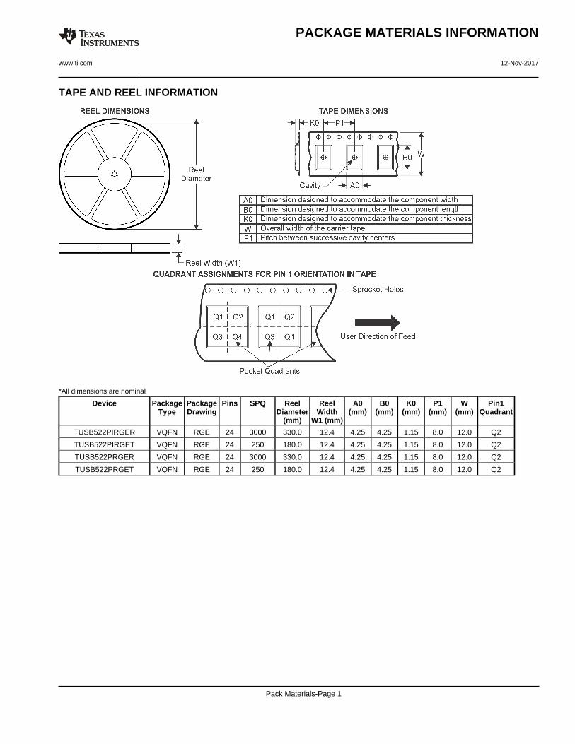
TAPE AND REEL INFORMATION
*All dimensions are nominal
Device PackageType
PackageDrawing
Pins SPQ ReelDiameter
(mm)
ReelWidth
W1 (mm)
A0(mm)
B0(mm)
K0(mm)
P1(mm)
W(mm)
Pin1Quadrant
TUSB522PIRGER VQFN RGE 24 3000 330.0 12.4 4.25 4.25 1.15 8.0 12.0 Q2
TUSB522PIRGET VQFN RGE 24 250 180.0 12.4 4.25 4.25 1.15 8.0 12.0 Q2
TUSB522PRGER VQFN RGE 24 3000 330.0 12.4 4.25 4.25 1.15 8.0 12.0 Q2
TUSB522PRGET VQFN RGE 24 250 180.0 12.4 4.25 4.25 1.15 8.0 12.0 Q2
PACKAGE MATERIALS INFORMATION
www.ti.com 12-Nov-2017
Pack Materials-Page 1

*All dimensions are nominal
Device Package Type Package Drawing Pins SPQ Length (mm) Width (mm) Height (mm)
TUSB522PIRGER VQFN RGE 24 3000 367.0 367.0 35.0
TUSB522PIRGET VQFN RGE 24 250 210.0 185.0 35.0
TUSB522PRGER VQFN RGE 24 3000 367.0 367.0 35.0
TUSB522PRGET VQFN RGE 24 250 210.0 185.0 35.0
PACKAGE MATERIALS INFORMATION
www.ti.com 12-Nov-2017
Pack Materials-Page 2

IMPORTANT NOTICE
Texas Instruments Incorporated (TI) reserves the right to make corrections, enhancements, improvements and other changes to itssemiconductor products and services per JESD46, latest issue, and to discontinue any product or service per JESD48, latest issue. Buyersshould obtain the latest relevant information before placing orders and should verify that such information is current and complete.TI’s published terms of sale for semiconductor products (http://www.ti.com/sc/docs/stdterms.htm) apply to the sale of packaged integratedcircuit products that TI has qualified and released to market. Additional terms may apply to the use or sale of other types of TI products andservices.Reproduction of significant portions of TI information in TI data sheets is permissible only if reproduction is without alteration and isaccompanied by all associated warranties, conditions, limitations, and notices. TI is not responsible or liable for such reproduceddocumentation. Information of third parties may be subject to additional restrictions. Resale of TI products or services with statementsdifferent from or beyond the parameters stated by TI for that product or service voids all express and any implied warranties for theassociated TI product or service and is an unfair and deceptive business practice. TI is not responsible or liable for any such statements.Buyers and others who are developing systems that incorporate TI products (collectively, “Designers”) understand and agree that Designersremain responsible for using their independent analysis, evaluation and judgment in designing their applications and that Designers havefull and exclusive responsibility to assure the safety of Designers' applications and compliance of their applications (and of all TI productsused in or for Designers’ applications) with all applicable regulations, laws and other applicable requirements. Designer represents that, withrespect to their applications, Designer has all the necessary expertise to create and implement safeguards that (1) anticipate dangerousconsequences of failures, (2) monitor failures and their consequences, and (3) lessen the likelihood of failures that might cause harm andtake appropriate actions. Designer agrees that prior to using or distributing any applications that include TI products, Designer willthoroughly test such applications and the functionality of such TI products as used in such applications.TI’s provision of technical, application or other design advice, quality characterization, reliability data or other services or information,including, but not limited to, reference designs and materials relating to evaluation modules, (collectively, “TI Resources”) are intended toassist designers who are developing applications that incorporate TI products; by downloading, accessing or using TI Resources in anyway, Designer (individually or, if Designer is acting on behalf of a company, Designer’s company) agrees to use any particular TI Resourcesolely for this purpose and subject to the terms of this Notice.TI’s provision of TI Resources does not expand or otherwise alter TI’s applicable published warranties or warranty disclaimers for TIproducts, and no additional obligations or liabilities arise from TI providing such TI Resources. TI reserves the right to make corrections,enhancements, improvements and other changes to its TI Resources. TI has not conducted any testing other than that specificallydescribed in the published documentation for a particular TI Resource.Designer is authorized to use, copy and modify any individual TI Resource only in connection with the development of applications thatinclude the TI product(s) identified in such TI Resource. NO OTHER LICENSE, EXPRESS OR IMPLIED, BY ESTOPPEL OR OTHERWISETO ANY OTHER TI INTELLECTUAL PROPERTY RIGHT, AND NO LICENSE TO ANY TECHNOLOGY OR INTELLECTUAL PROPERTYRIGHT OF TI OR ANY THIRD PARTY IS GRANTED HEREIN, including but not limited to any patent right, copyright, mask work right, orother intellectual property right relating to any combination, machine, or process in which TI products or services are used. Informationregarding or referencing third-party products or services does not constitute a license to use such products or services, or a warranty orendorsement thereof. Use of TI Resources may require a license from a third party under the patents or other intellectual property of thethird party, or a license from TI under the patents or other intellectual property of TI.TI RESOURCES ARE PROVIDED “AS IS” AND WITH ALL FAULTS. TI DISCLAIMS ALL OTHER WARRANTIES ORREPRESENTATIONS, EXPRESS OR IMPLIED, REGARDING RESOURCES OR USE THEREOF, INCLUDING BUT NOT LIMITED TOACCURACY OR COMPLETENESS, TITLE, ANY EPIDEMIC FAILURE WARRANTY AND ANY IMPLIED WARRANTIES OFMERCHANTABILITY, FITNESS FOR A PARTICULAR PURPOSE, AND NON-INFRINGEMENT OF ANY THIRD PARTY INTELLECTUALPROPERTY RIGHTS. TI SHALL NOT BE LIABLE FOR AND SHALL NOT DEFEND OR INDEMNIFY DESIGNER AGAINST ANY CLAIM,INCLUDING BUT NOT LIMITED TO ANY INFRINGEMENT CLAIM THAT RELATES TO OR IS BASED ON ANY COMBINATION OFPRODUCTS EVEN IF DESCRIBED IN TI RESOURCES OR OTHERWISE. IN NO EVENT SHALL TI BE LIABLE FOR ANY ACTUAL,DIRECT, SPECIAL, COLLATERAL, INDIRECT, PUNITIVE, INCIDENTAL, CONSEQUENTIAL OR EXEMPLARY DAMAGES INCONNECTION WITH OR ARISING OUT OF TI RESOURCES OR USE THEREOF, AND REGARDLESS OF WHETHER TI HAS BEENADVISED OF THE POSSIBILITY OF SUCH DAMAGES.Unless TI has explicitly designated an individual product as meeting the requirements of a particular industry standard (e.g., ISO/TS 16949and ISO 26262), TI is not responsible for any failure to meet such industry standard requirements.Where TI specifically promotes products as facilitating functional safety or as compliant with industry functional safety standards, suchproducts are intended to help enable customers to design and create their own applications that meet applicable functional safety standardsand requirements. Using products in an application does not by itself establish any safety features in the application. Designers mustensure compliance with safety-related requirements and standards applicable to their applications. Designer may not use any TI products inlife-critical medical equipment unless authorized officers of the parties have executed a special contract specifically governing such use.Life-critical medical equipment is medical equipment where failure of such equipment would cause serious bodily injury or death (e.g., lifesupport, pacemakers, defibrillators, heart pumps, neurostimulators, and implantables). Such equipment includes, without limitation, allmedical devices identified by the U.S. Food and Drug Administration as Class III devices and equivalent classifications outside the U.S.TI may expressly designate certain products as completing a particular qualification (e.g., Q100, Military Grade, or Enhanced Product).Designers agree that it has the necessary expertise to select the product with the appropriate qualification designation for their applicationsand that proper product selection is at Designers’ own risk. Designers are solely responsible for compliance with all legal and regulatoryrequirements in connection with such selection.Designer will fully indemnify TI and its representatives against any damages, costs, losses, and/or liabilities arising out of Designer’s non-compliance with the terms and provisions of this Notice.
Mailing Address: Texas Instruments, Post Office Box 655303, Dallas, Texas 75265Copyright © 2017, Texas Instruments Incorporated