tutorial introduction - nxp semiconductors€¦ · shift register spte sprf sptie sprie xxxx xxxx 0...
TRANSCRIPT

Tutorial Introduction
PURPOSE- To explain how to configure and use the Serial Peripheral Interface Module
OBJECTIVES:- Describe the uses and features of the Serial Peripheral Module.- Identify the steps to configure the Serial Peripheral Module.- Describe the master-slave data transmission process.- Write a program to configure a master module for data transmission.
CONTENTS:- 17 pages- 2 questions- 1 off-line programming exercise
LEARNING TIME:- 30 minutes
PREREQUESITE:- 68HC08 CPU Training Module
Welcome to this tutorial on the 68HC08 Serial Peripheral Interface (SPI) Module. This tutorial describes the features and configuration of the SPI Module. Please note that on subsequent pages, you will find reference buttons in the upper right of the content window that access additional content.
Upon completion of this tutorial, you’ll be able to describe the uses and features of the SPI Module, configure the SPI to operate in master or slave mode, and describe the master-slave data transmission process. You’ll also write a program to configure a master SPI for data transmission.
The recommended prerequisite for this tutorial is the 68HC08 CPU training module. Click the Forward arrow when you’re ready to begin the tutorial.

SPI Uses and Features
• Full-duplex synchronous serial operation• Smaller packages• Lower cost
• Maximum master mode frequency = bus frequency / 2 • Maximum slave mode frequency = bus frequency• Serial clock with programmable polarity and phase• Two separately enabled interrupts:
• SPRF (SPI Receiver Full)• SPTE (SPI Transmitter Empty)
Let’s begin this tutorial with a discussion of the uses and features of the SPI Module.
The SPI is a full-duplex synchronous serial communications module. It is intended primarily for communications within a PCB board at relatively high speeds. The SPI provides a cost effective way to interface serially with external peripherals. Some examples are: serial EEPROM, higher resolution analog-to-digital converters, digital-to-analog converters, LCD Modules, and shift registers. By communicating serially, the MCU and the peripherals require fewer pins. This results in smaller packages and usually lowers the cost. You can also use the SPI to communicate with other MCUs or processors.
The SPI operates in either master mode or slave mode. In master mode, the SPI generates the synchronous communication clock at one of four master frequencies. The maximum master mode frequency is half the bus frequency. For most 68HC08 MCUs, the maximum bus frequency is 8 MHz, allowing up to 4 MHz master mode clock rates.
In slave mode, the SPI can operate at clock rates up to the bus frequency, or 8 MHz in most 68HC08 MCUs.
The SPI is configurable for both polarity and phase enabling the SPI to communicate with most serial peripherals.
You can configure the SPI to generate two separate interrupt events: transmitter empty and receiver full. Each interrupt has a separate vector allowing for efficient transfers.
The remainder of this tutorial covers the configuration of the SPI for master-slave operations.

CLOCKLOGIC
TRANSMIT DATA REGISTER
RECIVE DATA REGISTER
INTERNAL BUS
SHIFT REGISTER
x x x x x x x x
SPSCK
MISO
MOSI
PINCONTROL
LOGIC
M
S
Master MCU Slave MCU
SS VDD
SS
SHIFT REGISTER
SPTE SPRF
SPRIESPTIE
x x x x x x x x
0 0
0 0
1 1
Master-Slave Overview
TRANSMIT DATA REGISTER
RECIVE DATA REGISTER
INTERNAL BUS
The SPI is built around a double buffered 8-bit shift register with both ends of the shift register brought out to MCU pins. One end of the shift register is connected to the master-in slave-out pin, MISO. This pin acts as an input for the master SPI Module and as an output for the slave SPI Module. The other end of the shift register is connected to MOSI pin.
The CPU begins a serial SPI transfer by writing a byte of data to the master’s SPI transmit data register. All 8-bits of data will be automatically transferred serially out the master’s MOSI pin synchronized to the master’s SPSCK clock output. For each bit shifted out of the master’s MOSI pin, a bit is shifted in through the master’s MISO pin allowing full duplex communication. A more detailed transfer example will be shown after we review the SPI module further.

3
BAUD RATEGENERATOR
SHIFT REGISTER
SHIFT REGISTER
MASTER MCU SLAVE MCU
SPSCK
MISO
MOSI
MISO
MOSISPSCK
SS VDDSS
Master-Slave Connections
Next, let’s look at the SPI master-slave connections. Connect the master MCU to the slave as shown in the figure. Note that before you enable the SPI Modules, you must configure them as a master and slave SPI.
Enable the master SPI by tying the master's slave select pin, SS, to VDD.
Before enabling the slave SPI, tie the slave's SS pin to ground. This allows a master to select which slave to communicate with. Typically, the master will use its I/O pins to drive the slave’s SS pin. Note that if a slave’s SS pin is set to 1, the slave's MISO pin is placed in a high-impedance state. When this occurs, the slave will ignore all incoming SPSCK clocks, even if it is already in the middle of a transmission.
You can configure and monitor SPI operations using the three SPI Module registers. Let‘s look at each register in detail, beginning with the SPI control register.

SPI Control Register (SPCR)
SPRIE - SPI Interrupt Enable Bit
1 - SPRF CPU interrupt requests enabled0 - SPRF CPU interrupt requests disabled
The figure shows the the SPI control register, SPCR. Let’s review each control bit in detail.
The receiver interrupt enable bit, SPRIE, is a read/write bit that enables CPU interrupt requests. When the SPRIE bit is set to 1, an interrupt is generated when the SPI receiver full bit, SPRF, is set. The SPRF bit is set when a byte of data is transferred to the SPI receive data register.
The DMA select bit, DMAS, is a read-only bit that has no effect on 68HC08 MCUs that do not have a DMA controller.
The SPI master bit, SPMSTR, is a read/write bit that selects the SPI mode of operation. Set the bit to 1 to select master mode and 0 to select slave mode.
The clock polarity bit, CPOL, is a read/write bit that determines the logic state of the SPSCK pin between transmissions. To transmit data between two SPI modules, the SPI modules must have identical CPOL values.

SPI Control Register (SPCR)
SPRIE - SPI Interrupt Enable Bit
1 - SPRF CPU interrupt requests enabled0 - SPRF CPU interrupt requests disabled
The clock phase bit, CPHA, is a read/write bit that controls the timing relationship between the serial clock and SPI data. To transmit data between two SPI modules, the SPI modules must have identical CPHA values. We will examine phase and polarity later in the tutorial.
The wired-OR mode bit, SPWOM, is a read/write bit that disables the pullup devices on pins SPSCK, MOSI, and MISO so that these pins become open-drain outputs.
The SPI enable bit, SPE, is a read/write bit that enables the SPI module. Note, you must disable the SPI before changing clock phase or polarity by writing to the CPOL or the CPHA bit.
The SPI transmit interrupt enable bit, SPTIE, is a read/write bit that enables CPU interrupt requests to be generated when a byte transfers from the transmit data register to the shift register.

SPI Status and Control Register (SPSCR)
Display bit annotation here.
The SPI Status and Control Register, SPSCR, contains status flags and additional control bits.
The SPI receiver full bit, SPRF, is a read-only bit that is set each time a byte transfers from the shift register to the receive data register. If the SPRIE bit in the SPCR is set, setting SPRF generates a CPU interrupt request. During an SPRF CPU interrupt, the CPU clears SPRF by reading the SPI status and control register with the SPRF bit set and then reading the SPI data register.
The error interrupt enable bit, ERRIE, is a read/write bit that enables the SPI to generate interrupts on error conditions to take corrective actions. The two error conditions are overflow and mode fault.
The overflow bit, OVRF, is a read-only bit that is set when the software does not read the byte in the receive data register before the next full byte enters the shift register. In an overflow condition, the last byte that was shifted is lost. You can clear the OVRF bit by reading the SPI status and control register with the OVRF set and then reading the receive data register.
The mode fault bit, MODF, is a read-only flag that is set when a mode fault error occurs during transmission and the mode fault enable bit, MODFEN, bit is set to 1. The conditions under which the MODF flag is set are different for master and slave SPIs. In a master SPI, the MODF bit is set whenever the SS pin goes low. In a slave SPI, the MODF bit is set when the SS pin goes high during transmission.
The transmitter empty bit, SPTE, is a read-only bit that is set each time the transmit data register transfers a byte to the shift register. Setting SPTE generates an interrupt if enabled by SPTIE. Note, you shouldn’t write to the SPI data register unless the SPTE bit is set.
The SPI Baud Rate Select Bits, SPR1 and SPR0, are read/write bits that select one of four baud rate divisors. Since the clock is driven only in master mode, these bits have no effect in slave mode.

Master Baud Rate Selection
Let’s take a closer look at how the baud rate is calculated. The table shows the bit codes for selecting one of four baud rate divisors using the SPI baud rate select bits (SPR1 and SPR0). The baud rate is calculated by dividing the bus frequency by two times the baud rate divisor.
For example, let’s assume a bus frequency of 8 Mhz. Setting both SPR1 and SPR0 to 0 selects the baud rate divisor 2. The bus frequency, 8 Mhz, divided by two times the baud rate divisor, or 4, gives a baud rate of 2 Mhz.

SPI Data Register (SPDR)
The SPI data register is actually two registers that you access with one address. The two registers are the receive data register and the transmit data register. These are separate registers that contain different values. You access the individual registers using the read/write actions. Reading the SPI data register reads data from the receive data register. Writing to the SPI data register writes data into the transmit data register.
Do not use read-modify-write instructions on the SPI data register since the register read is not the same as the register written.
On reset, the state of the registers is undefined.

Master-Slave Initialization
Step Control Bits
1) Initialize SPI clock frequency. SPR1 and SPR0 in SPSCR2) Configure the clock. CPOL and CPHA in SPSCR3) Select master/slave mode. SPMSTR in SPCR4) Enable interrupts if desired. SPTIE and SPRIE in SPCR 5) Enable master SPI. SPE in SPCR6) Enable slave SPIs. SPE in SPCR
Next, let’s review the steps to configure the SPI for data transmission using SPSCR and the SPCR.
First, select the SPI clock frequency using the baud rate select bits (SPR1-SPR0). Then configure the clock with the clock polarity bit (CPOL) and clock phase bit (CPHA).
Select the mode for each SPI using the SPI master bit (SPMSTR). Set the bit to 1 for the master SPI and 0 for the slave SPI. If interrupt driven operation is desired, enable interrupts using the SPI transmit interrupt enable bit (SPTIE) and the SPI receive interrupt enable bit (SPRIE).
Finally, enable the SPI system using SPI enable bit (SPE) in the control register. Make sure that the master SPI is enabled before the slave SPIs.

CLOCKLOGIC
TRANSMIT DATA REGISTER
RECIVE DATA REGISTER
INTERNAL BUS
SHIFT REGISTER
x x x x x x x x
SPSCK
MISO
MOSI
PINCONTROL
LOGICM
S
1 0 1 0 1 0 1 0
SHIFT REGISTER
1 0 1 0 1 0 1 0
MOSI
Master MCU Slave MCU
SS VDD
SS
SHIFT REGISTER
SPTE SPRF
SPRIESPTIE
x x x x x x x x1 0 1 0 1 0 1 0
0 0
0 0
1 1
Data Transmission Example
TRANSMIT DATA REGISTER
RECIVE DATA REGISTER1 0 1 0 1 0 1 0
INTERNAL BUS
Now that we’ve configured the SPI, let’s look at an example of master-slave data transmission.
The software begins an SPI transmission by writing a byte to the SPI transmit data register.
If the shift register is empty, the byte is immediately transferred to the shift register. Otherwise, the transfer begins when the shift register finishes transferring the previous byte.
Once the byte is transferred from the SPI transmit register to the shift register, the SPTE bit is set indicating that another byte can be written to the SPI transmit data register. The SPTE bit generates a CPU interrupt if the SPTIE bit is set to 1. This allows interrupt driven transmissions of multi-byte transfers. In this example, the SPTIE bit is set to 0, so that interrupts are disabled.
The byte begins shifting out a bit at a time on the MOSI pin synchronized with the master clock signal, SPSCK. The transfer will continue for 8 SPSCK clock cycles, transferring all 8-bits. As the byte shifts out from the master, another byte shifts in from the slave on the MISO pin. In this example, we will disregard the byte of information being shifted from the slave SPI to the master SPI.
The transmission ends when the whole byte is shifted out of the master SPI shift register and into the slave SPI shift register. The slave shift register is then automatically transferred to the slave SPI receive data register if it is empty, allowing another byte to transfer if one is pending.
The SPRF is set indicating that the SPI receive register is full and waiting to be read. If the SPRIE bit is set to 1, a SPI receive interrupt request is also generated. In this example, the SPRIE bit is set to 0.
To avoid overflow, the slave must read the receive data register prior to the master attempting to transfer more than one additional byte. For example, if the master has successfully transmitted a byte that is waiting to be read in the receive data register, the master may transfer an additional byte. This additional byte will be held in the shift register and not loaded into the receive register since the previous byte has not been read by the CPU. If the master attempts to serially transmit another byte prior to reading the receive data register, the data in the slave shift register will be overwritten causing an overflow error condition. The byte in the receive data register is not overwritten.
SPSCK cycle #from reference
SPSCK; CPOL = 0
SPSCK; CPOL =1
MOSIfrom master
MISOfrom slave
SS; to slave
Capture strobe
1 2 3 4 5 6 7 8
MSB
MSB
BIT 6
BIT 6
BIT 5
BIT 5
BIT 4
BIT 4
BIT 3
BIT 3
LSB
LSBBIT 1
BIT 1
BIT 2
BIT 2
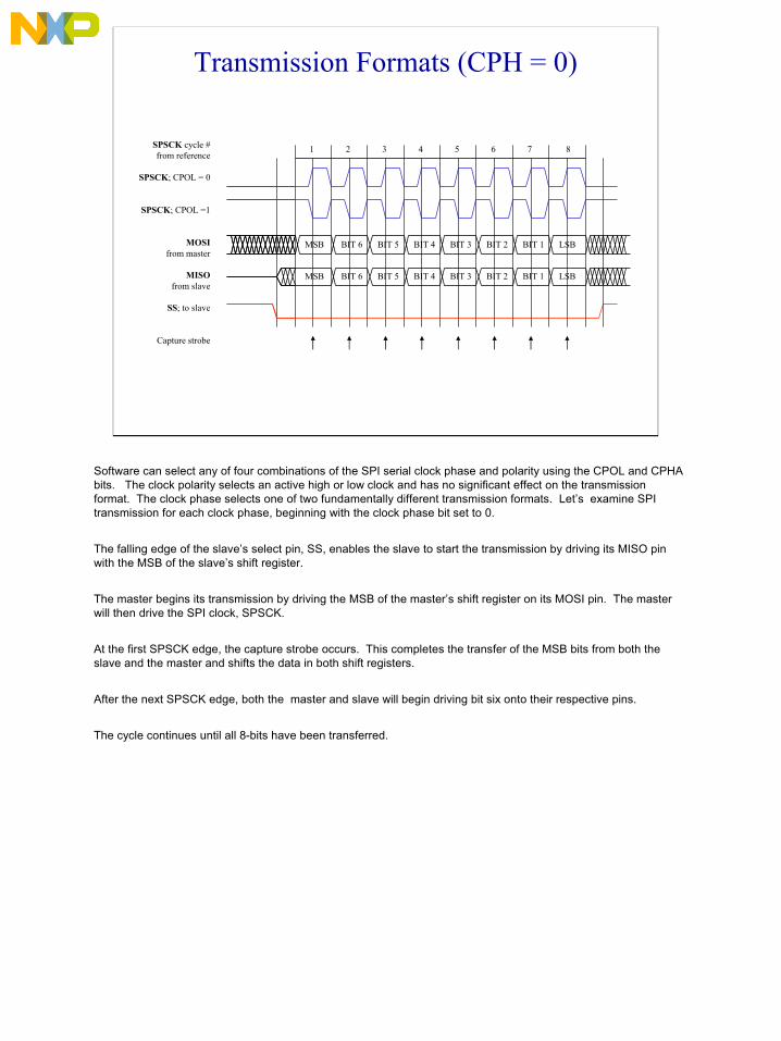
Transmission Formats (CPH = 0)
Software can select any of four combinations of the SPI serial clock phase and polarity using the CPOL and CPHA bits. The clock polarity selects an active high or low clock and has no significant effect on the transmission format. The clock phase selects one of two fundamentally different transmission formats. Let’s examine SPI transmission for each clock phase, beginning with the clock phase bit set to 0.
The falling edge of the slave’s select pin, SS, enables the slave to start the transmission by driving its MISO pin with the MSB of the slave’s shift register.
The master begins its transmission by driving the MSB of the master’s shift register on its MOSI pin. The master will then drive the SPI clock, SPSCK.
At the first SPSCK edge, the capture strobe occurs. This completes the transfer of the MSB bits from both the slave and the master and shifts the data in both shift registers.
After the next SPSCK edge, both the master and slave will begin driving bit six onto their respective pins.
The cycle continues until all 8-bits have been transferred.

Transmission Formats (CPH = 1)
SPSCK cycle #from reference
SPSCK; CPOL = 0
SPSCK; CPOL =1
MOSIfrom master
MISOfrom slave
SS; to slave
Capture strobe
1 2 3 4 5 6 7 8
MSB
MSB
BIT 6
BIT 6
BIT 5
BIT 5
BIT 4
BIT 4
BIT 3
BIT 3
LSB
LSBBIT 1
BIT 1
BIT 2
BIT 2MSB
MSB
BIT 6
BIT 6
BIT 5
BIT 5
BIT 4
BIT 4
BIT 3
BIT 3
LSB
LSBBIT 1
BIT 1
BIT 2
BIT 2
Next, we’ll examine SPI transmissions with the clock phase polarity set to 1.
When the slave’s SS pin goes low, the slave waits until the first edge of SPSCK to drive its MISO pin.
The MSB bits from the master and the slave are driven on their respective pins at the first edge of SPSCK.
The capture strobe occurs at the second edge of SPSCK with CPH set to 1 instead of the first edge when CPH is cleared to 0.
Finally, the cycle continues until all 8-bits have been transferred.

Question
With the bus frequency set to 16 Mhz and the SPI baud rate select bits set to10, what is the master SPI baud rate?
a) 0.25 MHzb) 1 MHzc) 2 MHzd) 4 MHz
Let’s consider a couple of questions to check your understanding of the material.
With the bus frequency set to 16 Mhz and the SPI baud rate select bits set to 10, what is the master SPI baud rate? Click on your choice.
Answer: The baud rate is the bus frequency divided by two times the baud rate divisor. The bit code 10 selects the baud rate divisor 32. Dividing the bus frequency, 16 MHz, by two times the baud rate divisor, or 64, gives a baud rate of 0.25 MHz.

Question
What happens when the master SPI attempts to send another byte to theslave SPI, when the slave SPI receive data register contains a byte of datapreviously transmitted but not yet read by the slave CPU? Click on yourchoice.
a) No transmission occursb) All 8-bits are transfered from the master’s shift register to the
slave’s shift register, while data in the slave’s receive data register is overwritten.
c) All 8-bits transferred from the master’s shift register to the slave’s shift register, while data in the slave’s receive data register is not overwritten until the CPU first reads the slave’s receivedata register.
What happens when the master SPI attempts to send another byte to the slave SPI, when the slave SPI receive data register contains a byte of data previously transmitted but not yet read by the slave CPU? Click on your choice.
Answer: All 8-bits are transferred from the master’s shift register to the slave’s shift register, while data in the slave’s receive data register is not overwritten until the CPU first reads the slave’s receive data register. This double buffering allows one extra byte to be transmitted prior to reading the previous transmission with no loss of data.

Programming Exercise
• Configure a non-interrupt driven master.• Transmit the value $55.• Use a serial-in/parallel-out, 8-bit shift register:
• Register is chip-selected with the port PB3 line at a low voltage level.• Verify that the PB3 line is high between transfers.
• Configure the SPI clock: • Idle low and take data on rising clock edges.• SPI clock frequency < 300 kHz.• Assume system clock frequency of 8 MHz.
Let’s complete this tutorial with an off-line programming exercise. Let’s write a program to configure the master SPI for data transmission. In this exercise, we’ll perform a polled SPI transfer of one byte to a serial-in/parallel-out 8-bit shift register. We could use this program to provide additional latched I/O ports through the shift register.
In your program, configure the SPI as a non-interrupt driven master. Transmit one byte of data containing the value $55. The shift register should be chip-selected with the port B3 line using a low voltage select. Make sure that the BP3 line remains high between transfers .
Configure the SPI clock to idle low and take data on rising clock edges. Also, configure the SPI clock frequency to stay under 300 kHz, assuming a system clock frequency of 8 Mhz.
Take a moment to review the exercise instructions. When you are finished writing your program, click the Forward arrow to continue the tutorial and review the exercise solution.

PTB EQU $01 ; Port B Data register DDRB EQU $05 ; Port B Data Direction registerSPCR EQU $10 ; SPI Control register SPSCR EQU $11 ; SPI Status and Control registerSPDR EQU $12 ; SPI Data (Read=rcv, Write=xmt)
;; Select Port B inputs/outputs & levels:;
BSET #3,PTB ; Make PB3 output value high BSET #3,DDRB ; Make PB3 an outputLDA #$06 ; Load accumulator (ACC) with:
; " MOSI & SPSCK = outputs" value; " MISO & SS* = inputs" value
STA DDRF ; Store ACC to DDRF register;; Select master mode, clock, and enable SPI:
LDA #$02 ; Load ACC with value that selects 300 kHzSTA SPSCR ; Store ACC to SPSCRLDA #$22 ; Load ACC with value to configure SPSCRSTA SPCR ; Store ACC to SPCR
;; Send $55 to shift register:;
BCLR #3,PORTB ; Make PB3 output low (chip-select register)LDA #$55 ; Load ACC with $55STA SPDR ; Store ACC to SPDR
WAIT BRCLR #7,SPSCR,WAIT ; Wait until transmission is completeBSET #3,PORTB ; Make PB3 output high (deselect register)
DONE BRA DONE ; Done, stay here
SPI Exercise Solution
Next, compare your main program with the one provided in the solution.

Tutorial Completion
- SPI Uses and Features - SPI Configuration- SPI Master-Slave Data Transmission
In this tutorial, you’ve had an opportunity to work with the 68HC08 SPI Module. You’ve learned how to configure the SPI Module for master mode and slave mode. You’ve also written a program to configure a non-interrupt driven master SPI to transfer data to a chip-selected shift register.