tutorial: working with the xilinx tools 14
TRANSCRIPT
Tutorial: Working with the Xilinx tools 14.4
This tutorial will show you how to:
Part I: Set up a new project in ISE
Part II: Implement a function using Schematics
Part III: Implement a function using Verilog
Part IV: Simulate the schematic/Verilog circuit using the ISIM and a Verilog test fixture
Part V: Synthesize, Implement, Generate, and program the Nexys 3 FPGA board
I assume that you’re using a DSL lab machine, or that you’ve installed Xilinx ISE 14.4 on your own
machine as some of the following procedures may be different depending on the version of ISE.
Part I: Setting up a New Project
Attention: Make sure to use the appropriate version of the ISE, 64 bit navigator for a 64 bit
OS, and 32 bit for 32 bit. If you don’t pay attention to this, there will be
unexpected behavior in the ISE software and thing may not work properly!
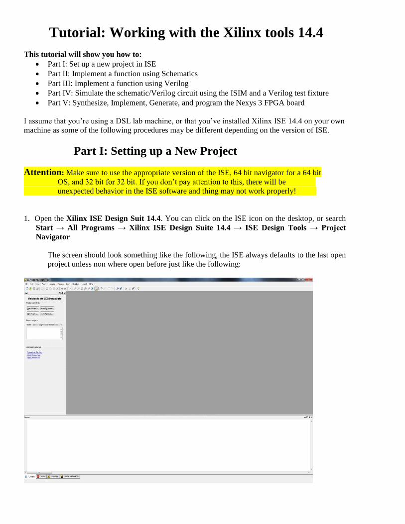
1. Open the Xilinx ISE Design Suit 14.4. You can click on the ISE icon on the desktop, or search
Start → All Programs → Xilinx ISE Design Suite 14.4 → ISE Design Tools → Project
Navigator
The screen should look something like the following, the ISE always defaults to the last open
project unless non where open before just like the following:

2. Now either press the New Project tab or select File → New Project… and change the Name
and Location to whatever you like.
Attention: Xilinx does not allow spaces in path or file names! For example “C:\ECE 3700
will not work, same for the file name! Use the under_score for spaces if you need to.
The selected Top Level Source Type is Schematic because that’s what we’re planning on
using first. This is not critical, as you can always add a new source file of any type later. The
dialog box for the project wizard looks like:
3. Click NEXT and in the next dialog box you should fill in the fields as shown here. You can
do this in two ways, one is to select an “Evaluation Development Board” from the drop
down list, in our case you should select “Nexys 3”. This will automatically fill out the board
information in the next five sections. If the board does not exist in the list then you can set
correct choises according to following image.
We are using a General Purpose Product in the Xilinx Spartan6 family. The specific chip
on our board is an XC6SLX16 in a CSG324 package and the –3 speed grade.
Attention: If you fail to set the correct options in this part, you will not be able to
implement your design and program it on the Nexys 3 board!
Please make sure that the Synthesis Tool is XST, the Simulator is the ISIM, and the
Preferred Language is Verilog. This is very important for proper operation
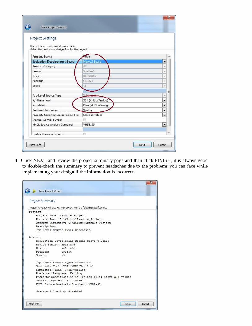
4. Click NEXT and review the project summary page and then click FINISH, it is always good
to double-check the summary to prevent headaches due to the problems you can face while
implementing your design if the information is incorrect.

Part II: Implement a function using Schematics
1. Now you should have a new project that targets the correct Xilinx part and other features of
the ISE system. Notice the window to the left, and also notice the four tabs Start, Design,
Files, …, and in the case of an open schematic a Symbols tab will appear. Ensure that the
“Implementation” choise is selected on the design pane.
2. Now you want to create a new schematic in your project. Choose Project → New Source
or right click on the Hierarchy section of the design windows to get the dialog box that
adds a new source file to your project (or use the New Source widget on the left vertical
tool bar). Source files can be of many types. We’ll add a Schematic named simple_logic.
Make sure to both fill in the File Name and select the Schematic type from the list on the
left. I’ve filled in my dialog box as shown below. Now click NEXT and after observing the
summary page click FINISH.
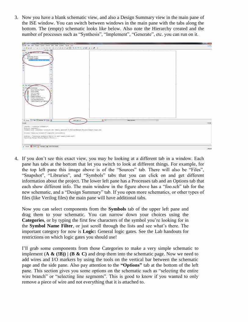
3. Now you have a blank schematic view, and also a Design Summary view in the main pane of
the ISE window. You can switch between windows in the main pane with the tabs along the
bottom. The (empty) schematic looks like below. Also note the Hierarchy created and the
number of processes such as “Synthesis”, “Implement”, “Generate”, etc. you can run on it.
4. If you don’t see this exact view, you may be looking at a different tab in a window. Each
pane has tabs at the bottom that let you switch to look at different things. For example, for
the top left pane this image above is of the “Sources” tab. There will also be “Files”,
“Snapshot”, “Libraries”, and “Symbols” tabs that you can click on and get different
information about the project. The lower left pane has a Processes tab and an Options tab that
each show different info. The main window in the figure above has a “foo.sch” tab for the
new schematic, and a “Design Summary” tab. If you open more schematics, or other types of
files (like Verilog files) the main pane will have additional tabs.
Now you can select components from the Symbols tab of the upper left pane and
drag them to your schematic. You can narrow down your choices using the
Categories, or by typing the first few characters of the symbol you’re looking for in
the Symbol Name Filter, or just scroll through the lists and see what’s there. The
important category for now is Logic: General logic gates. See the Lab handouts for
restrictions on which logic gates you should use!
I’ll grab some components from those Categories to make a very simple schematic to
implement (A & (!B)) | (B & C) and drop them into the schematic page. Now we need to
add wires and I/O markers by using the tools on the vertical bar between the schematic
page and the side pane. Also pay attention to the “Options” tab at the bottom of the left
pane. This section gives you some options on the schematic such as “selecting the entire
wire branch” or “selecting line segments”. This is good to know if you wanted to only
remove a piece of wire and not everything that it is attached to.

5. Use the wiring tool to wire up the components. It is in the tool bar and looks like a red
line and a pencil. You could also use Add →Wire from the menu. I’m using the following
components (from the Logic category) in this example:
a. and2: a two-input AND gate
b. or2: a two-input OR gate
c. inv: an inverter
6. Now place I/O Markers to the inputs and outputs. I’ve used the I/O Marker widget
that looks like two little labels. You can also use the Add → I/O Marker command from the
menu. Click on the endpoints of the wire to add the marker.
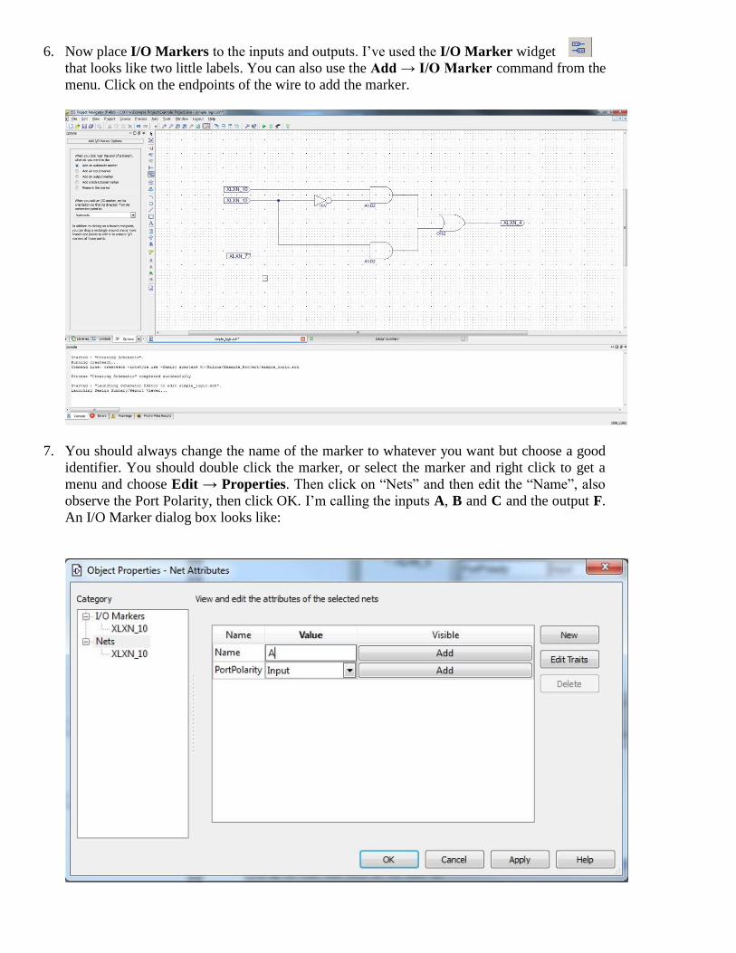
7. You should always change the name of the marker to whatever you want but choose a good
identifier. You should double click the marker, or select the marker and right click to get a
menu and choose Edit → Properties. Then click on “Nets” and then edit the “Name”, also
observe the Port Polarity, then click OK. I’m calling the inputs A, B and C and the output F.
An I/O Marker dialog box looks like:
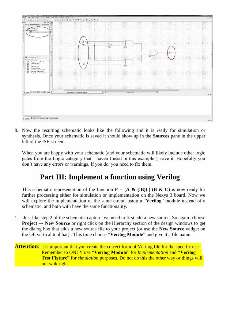
8. Now the resulting schematic looks like the following and it is ready for simulation or
synthesis. Once your schematic is saved it should show up in the Sources pane in the upper
left of the ISE screen.
When you are happy with your schematic (and your schematic will likely include other logic
gates from the Logic category that I haven’t used in this example!), save it. Hopefully you
don’t have any errors or warnings. If you do, you need to fix them.
Part III: Implement a function using Verilog
This schematic representation of the function F = (A & (!B)) | (B & C) is now ready for
further processing either for simulation or implementation on the Nexys 3 board. Now we
will explore the implementation of the same circuit using a “Verilog” module instead of a
schematic, and both with have the same functionality.
1. Just like step 2 of the schematic capture, we need to first add a new source. So again choose
Project → New Source or right click on the Hierarchy section of the design windows to get
the dialog box that adds a new source file to your project (or use the New Source widget on
the left vertical tool bar) . This time choose “Verilog Module” and give it a file name.
Attention: it is important that you create the correct form of Verilog file for the specific use.
Remember to ONLY use “Verilog Module” for Implementation and “Verilog
Test Fixture” for simulation purposes. Do not do this the other way or things will
not wok right
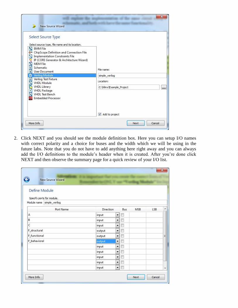
2. Click NEXT and you should see the module definition box. Here you can setup I/O names
with correct polarity and a choice for buses and the width which we will be using in the
future labs. Note that you do not have to add anything here right away and you can always
add the I/O definitions to the module’s header when it is created. After you’re done click
NEXT and then observe the summary page for a quick review of your I/O list.
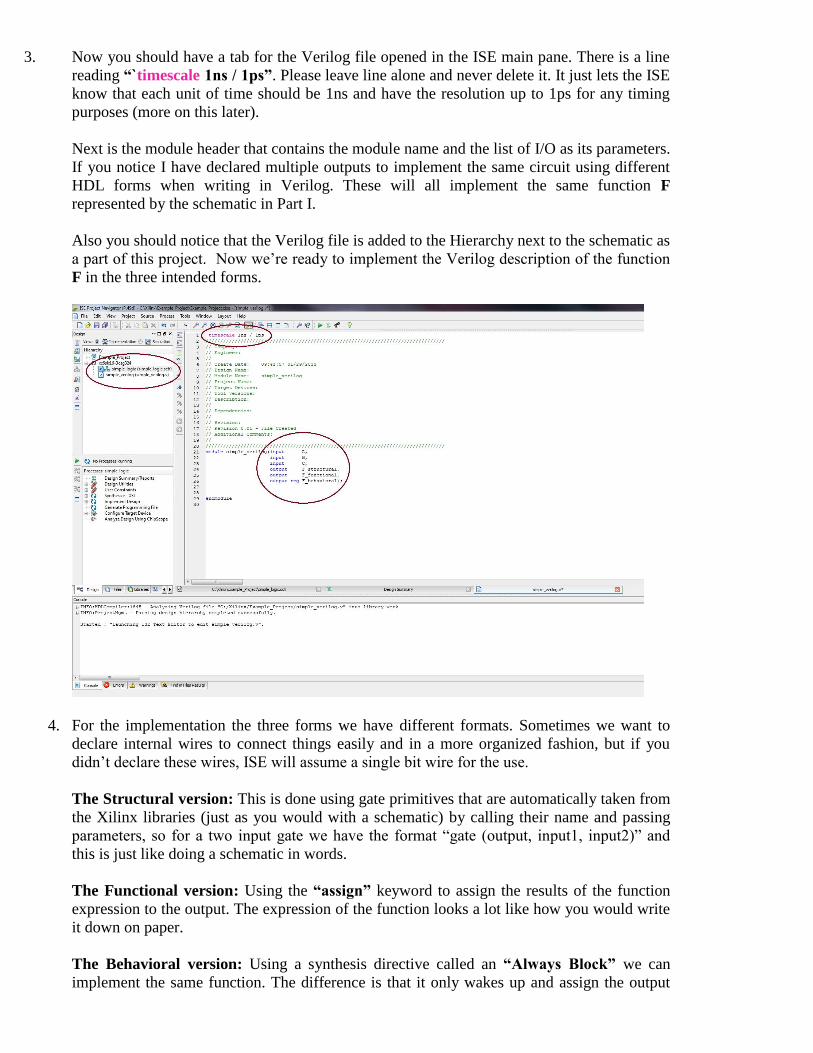
3. Now you should have a tab for the Verilog file opened in the ISE main pane. There is a line
reading “`timescale 1ns / 1ps”. Please leave line alone and never delete it. It just lets the ISE
know that each unit of time should be 1ns and have the resolution up to 1ps for any timing
purposes (more on this later).
Next is the module header that contains the module name and the list of I/O as its parameters.
If you notice I have declared multiple outputs to implement the same circuit using different
HDL forms when writing in Verilog. These will all implement the same function F
represented by the schematic in Part I.
Also you should notice that the Verilog file is added to the Hierarchy next to the schematic as
a part of this project. Now we’re ready to implement the Verilog description of the function
F in the three intended forms.
4. For the implementation the three forms we have different formats. Sometimes we want to
declare internal wires to connect things easily and in a more organized fashion, but if you
didn’t declare these wires, ISE will assume a single bit wire for the use.
The Structural version: This is done using gate primitives that are automatically taken from
the Xilinx libraries (just as you would with a schematic) by calling their name and passing
parameters, so for a two input gate we have the format “gate (output, input1, input2)” and
this is just like doing a schematic in words.
The Functional version: Using the “assign” keyword to assign the results of the function
expression to the output. The expression of the function looks a lot like how you would write
it down on paper.
The Behavioral version: Using a synthesis directive called an “Always Block” we can
implement the same function. The difference is that it only wakes up and assign the output
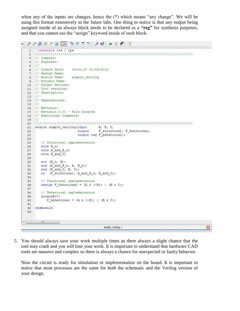
when any of the inputs are changes, hence the (*) which means “any change”. We will be
using this format extensively in the future labs. One thing to notice is that any output being
assigned inside of an always block needs to be declared as a “reg” for synthesis purposes,
and that you cannot use the “assign” keyword inside of such block.
5. You should always save your work multiple times as there always a slight chance that the
tool may crash and you will lose your work. It is important to understand that hardware CAD
tools are massive and complex so there is always a chance for unexpected or faulty behavior.
Now the circuit is ready for simulation or implementation on the board. It is important to
notice that most processes are the same for both the schematic and the Verilog version of
your design.

Part IV: Simulate the schematic/Verilog circuit
using the ISIM and a Verilog test fixture
Now that you have a saved schematic, you need to simulate its behavior. The simulator
we’ll use is the ISE built in simulator, which is essentially a Verilog simulator. The
schematic that you just drew will be saved as a piece of Verilog behind your back if you
choose to simulate it. In order to simulate the circuit you need:
Testbench: is a file that becomes a top module to your design and applies inputs to your
circuit, and potentially checks that the outputs are correct. This will be another Verilog file
written slightly differently than circuit implementation. The testbench will instantiate one
copy of your circuit, and call it UUT for “Unit Under Test”. You will then write the
Verilog statements that set the inputs to your circuit (the UUT), and looks at the outputs
produced by your circuit. You need to know only very basic Verilog syntax to do this.
1. First you need to ensure that the ISE more is changed to “Simulation” from implementation.
Go to the top left pane and change the “View” field to simulation. The design window will
then change slightly with different options. Referring back to the same step in creating a
“New Source” create a “Verilog Test Fixture” to create a Verilog file that will contain the
test code.
2. Click NEXT and choose which design you want to associate the test bench with. This is very
important as you will have multiple modules or schematics in the future and you need to be
sure which design will be going under test using the test bench. In this case I will just choose
the “simple_verilog” module to be tested. The procedure for testing the schematic version is
exactly the same, you just have to choose the appropriate source to be associated with the test
bench.
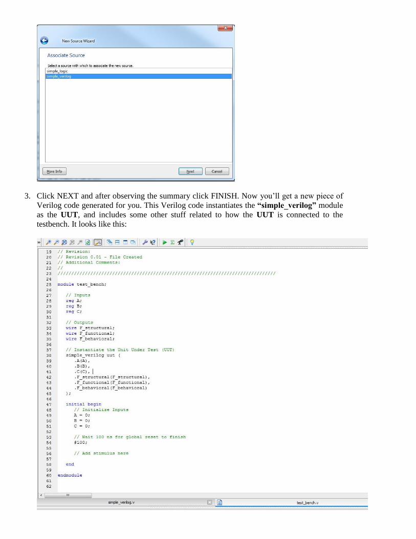
3. Click NEXT and after observing the summary click FINISH. Now you’ll get a new piece of
Verilog code generated for you. This Verilog code instantiates the “simple_verilog” module
as the UUT, and includes some other stuff related to how the UUT is connected to the
testbench. It looks like this:

4. You can now write your test bench code as an initial block right before the endmodule.
Basically you set the values of your inputs, and tell the simulator how long to wait
between each change on the inputs. The results will eventually be plotted on a waveform
for you. Verilog syntax for setting a variable is very simple, and the #50 notation just
means for the simulation to wait for 50 ticks of the simulation clock before moving on to
the next statement. A very simple test bench for this circuit looks like the following. I
added the lines between initial and end to drive the inputs with different values so that we
can see what the circuit result is. Note that each statement in Verilog ends with a
semicolon, and you can put multiple statements on a line if you like.
Later in upcoming labs we will explore different options that we can write the sequencing
of the inputs to prevent having to hardcode lots of input changes, you can see that if we
had two more inputs then we had to write out 32 different possibilities for 5 inputs. We
will see how using a “For” loop in the test bench will make things a lot and shorter.
5. We usually want to test all possible inputs to be able to draw a better conclusion on
whether the circuit is functioning correctly. After you’re satisfied with the input setting of
your test bench make sure to save. Always observe the console window to look out for
errors after saving.
Now you are ready to simulate your Verilog circuit. Observe that the test bench Verilog
file is now the top module to your “simple_verilog” module in the simulation design
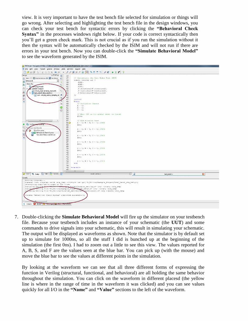
view. It is very important to have the test bench file selected for simulation or things will
go wrong. After selecting and highlighting the test bench file in the design windows, you
can check your test bench for syntactic errors by clicking the “Behavioral Check
Syntax” in the processes windows right below. If your code is correct syntactically then
you’ll get a green check mark. This is not crucial as if you run the simulation without it
then the syntax will be automatically checked by the ISIM and will not run if there are
errors in your test bench. Now you can double-click the “Simulate Behavioral Model”
to see the waveform generated by the ISIM.
7. Double-clicking the Simulate Behavioral Model will fire up the simulator on your testbench
file. Because your testbench includes an instance of your schematic (the UUT) and some
commands to drive signals into your schematic, this will result in simulating your schematic.
The output will be displayed as waveforms as shown. Note that the simulator is by default set
up to simulate for 1000ns, so all the stuff I did is bunched up at the beginning of the
simulation (the first 0ns). I had to zoom out a little to see this view. The values reported for
A, B, S, and F are the values seen at the blue bar. You can pick up (with the mouse) and
move the blue bar to see the values at different points in the simulation.
By looking at the waveform we can see that all three different forms of expressing the
function in Verilog (structural, functional, and behavioral) are all holding the same behavior
throughout the simulation. You can click on the waveform in different placesd (the yellow
line is where in the range of time in the waveform it was clicked) and you can see values
quickly for all I/O in the “Name” and “Value” sections to the left of the waveform.

The simulation is now done. You can always go back to the test bench and make a more
complicated set of tests and re-simulate the circuit.
It is good to observe the other capabilities of your simulation windows. The console is where
all of the simulator messages will be printed. Look for errors or warning about your design.
The left panes will allow you to dig into your design hierarchy to grab signals that are deep in
the design and may not be set in the top module, recall that the test bench is only created for
one module, so if you have a multiple level hierarchy then you need to use these windows to
navigate to the desired signal and drag-and-drop into the simulation windows.
Sometimes we want the values of the test bench results for the Verilog module’s output to be
printed into the console of the simulator windows. We can then add the Verilog print
statement called $display in between our test bench code. This will allow us to monitor
signals in large designs and long waveforms with many signals being looked at. We can also
format the printed statement to what we want it to show on the console for better readability
of the results.
Below are some $display statements added to the current test bench to show the effects it will
have. Never the less, you should always put a $display statement at the beginning and the end
of your test code to indicate the starting and actual finishing of the simulations.
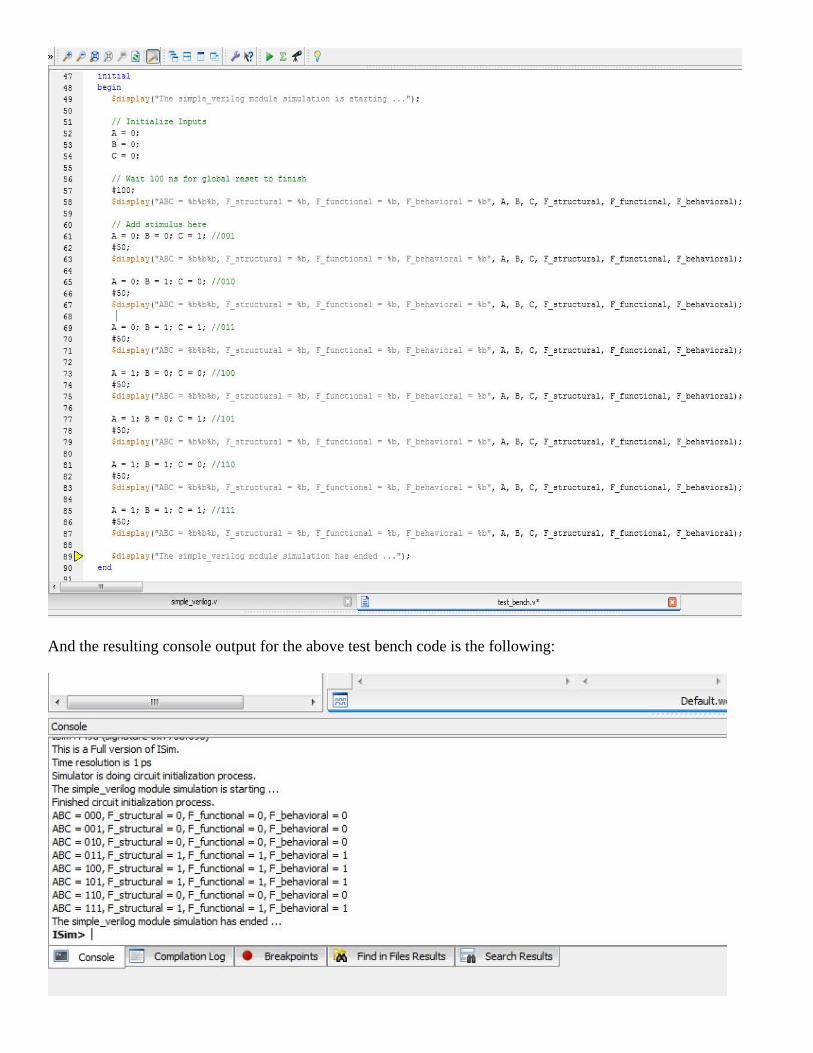
And the resulting console output for the above test bench code is the following:

Part V: Synthesize, Implement, Generate Bitstream,
and program the Nexys 3 FPGA board