tvp6000c data manual - digi-key sheets/texas instruments pdfs... · 2.11.41 dppl 2–33 ... 2–9...
TRANSCRIPT

TVP6000CData Manual
NTSC/PAL Digital Video Encoder
SLAS184July 1998
Printed on Recycled Paper

IMPORTANT NOTICE
Texas Instruments and its subsidiaries (TI) reserve the right to make changes to their products or to discontinueany product or service without notice, and advise customers to obtain the latest version of relevant informationto verify, before placing orders, that information being relied on is current and complete. All products are soldsubject to the terms and conditions of sale supplied at the time of order acknowledgement, including thosepertaining to warranty, patent infringement, and limitation of liability.
TI warrants performance of its semiconductor products to the specifications applicable at the time of sale inaccordance with TI’s standard warranty. Testing and other quality control techniques are utilized to the extentTI deems necessary to support this warranty. Specific testing of all parameters of each device is not necessarilyperformed, except those mandated by government requirements.
CERTAIN APPLICATIONS USING SEMICONDUCTOR PRODUCTS MAY INVOLVE POTENTIAL RISKS OFDEATH, PERSONAL INJURY, OR SEVERE PROPERTY OR ENVIRONMENTAL DAMAGE (“CRITICALAPPLICATIONS”). TI SEMICONDUCTOR PRODUCTS ARE NOT DESIGNED, AUTHORIZED, ORWARRANTED TO BE SUITABLE FOR USE IN LIFE-SUPPORT DEVICES OR SYSTEMS OR OTHERCRITICAL APPLICATIONS. INCLUSION OF TI PRODUCTS IN SUCH APPLICATIONS IS UNDERSTOOD TOBE FULLY AT THE CUSTOMER’S RISK.
In order to minimize risks associated with the customer’s applications, adequate design and operatingsafeguards must be provided by the customer to minimize inherent or procedural hazards.
TI assumes no liability for applications assistance or customer product design. TI does not warrant or representthat any license, either express or implied, is granted under any patent right, copyright, mask work right, or otherintellectual property right of TI covering or relating to any combination, machine, or process in which suchsemiconductor products or services might be or are used. TI’s publication of information regarding any thirdparty’s products or services does not constitute TI’s approval, warranty or endorsement thereof.
Copyright 1998, Texas Instruments Incorporated

iii
ContentsSection Title Page
1 Introduction 1–1. . . . . . . . . . . . . . . . . . . . . . . . . . . . . . . . . . . . . . . . . . . . . . . . . . . . . . . . . . . . . . . 1.1 Features 1–1. . . . . . . . . . . . . . . . . . . . . . . . . . . . . . . . . . . . . . . . . . . . . . . . . . . . . . . . . . . . . . 1.2 Applications 1–2. . . . . . . . . . . . . . . . . . . . . . . . . . . . . . . . . . . . . . . . . . . . . . . . . . . . . . . . . . . 1.3 Functional Block Diagram 1–2. . . . . . . . . . . . . . . . . . . . . . . . . . . . . . . . . . . . . . . . . . . . . . . 1.4 Terminal Assignments 1–3. . . . . . . . . . . . . . . . . . . . . . . . . . . . . . . . . . . . . . . . . . . . . . . . . . 1.5 Ordering Information 1–4. . . . . . . . . . . . . . . . . . . . . . . . . . . . . . . . . . . . . . . . . . . . . . . . . . . 1.6 Terminal Functions 1–4. . . . . . . . . . . . . . . . . . . . . . . . . . . . . . . . . . . . . . . . . . . . . . . . . . . . .
2 Detailed Description 2–1. . . . . . . . . . . . . . . . . . . . . . . . . . . . . . . . . . . . . . . . . . . . . . . . . . . . . . . 2.1 Initialization 2–1. . . . . . . . . . . . . . . . . . . . . . . . . . . . . . . . . . . . . . . . . . . . . . . . . . . . . . . . . . . 2.2 I2C Interface 2–3. . . . . . . . . . . . . . . . . . . . . . . . . . . . . . . . . . . . . . . . . . . . . . . . . . . . . . . . . . 2.3 Data Manager 2–4. . . . . . . . . . . . . . . . . . . . . . . . . . . . . . . . . . . . . . . . . . . . . . . . . . . . . . . . . 2.4 Scaling Processor 2–5. . . . . . . . . . . . . . . . . . . . . . . . . . . . . . . . . . . . . . . . . . . . . . . . . . . . . 2.5 Video Encoder 2–6. . . . . . . . . . . . . . . . . . . . . . . . . . . . . . . . . . . . . . . . . . . . . . . . . . . . . . . . .
2.5.1 Luminance Encoding 2–6. . . . . . . . . . . . . . . . . . . . . . . . . . . . . . . . . . . . . . . . . . . 2.5.2 Luminance Low-Pass and Interpolation Filter 2–6. . . . . . . . . . . . . . . . . . . . . . 2.5.3 Cross Color Reduction Filter 2–8. . . . . . . . . . . . . . . . . . . . . . . . . . . . . . . . . . . . 2.5.4 Chrominance Encoding 2–8. . . . . . . . . . . . . . . . . . . . . . . . . . . . . . . . . . . . . . . .
2.6 Closed Caption 2–9. . . . . . . . . . . . . . . . . . . . . . . . . . . . . . . . . . . . . . . . . . . . . . . . . . . . . . . . 2.7 Clock Generation 2–11. . . . . . . . . . . . . . . . . . . . . . . . . . . . . . . . . . . . . . . . . . . . . . . . . . . . . 2.8 Analog Output 2–11. . . . . . . . . . . . . . . . . . . . . . . . . . . . . . . . . . . . . . . . . . . . . . . . . . . . . . . . 2.9 Video Port Interface 2–12. . . . . . . . . . . . . . . . . . . . . . . . . . . . . . . . . . . . . . . . . . . . . . . . . . .
2.9.1 RCV1 2–12. . . . . . . . . . . . . . . . . . . . . . . . . . . . . . . . . . . . . . . . . . . . . . . . . . . . . . . 2.9.2 RCV2 2–12. . . . . . . . . . . . . . . . . . . . . . . . . . . . . . . . . . . . . . . . . . . . . . . . . . . . . . . 2.9.3 RCM1 2–12. . . . . . . . . . . . . . . . . . . . . . . . . . . . . . . . . . . . . . . . . . . . . . . . . . . . . . . 2.9.4 RCM2 2–13. . . . . . . . . . . . . . . . . . . . . . . . . . . . . . . . . . . . . . . . . . . . . . . . . . . . . . .
2.10 Modes of Operation 2–13. . . . . . . . . . . . . . . . . . . . . . . . . . . . . . . . . . . . . . . . . . . . . . . . . . . 2.10.1 Master Mode 2–13. . . . . . . . . . . . . . . . . . . . . . . . . . . . . . . . . . . . . . . . . . . . . . . . . 2.10.2 Slave Mode 2–13. . . . . . . . . . . . . . . . . . . . . . . . . . . . . . . . . . . . . . . . . . . . . . . . . . 2.10.3 Demand Mode 2–14. . . . . . . . . . . . . . . . . . . . . . . . . . . . . . . . . . . . . . . . . . . . . . . 2.10.4 Genlock Mode 2–14. . . . . . . . . . . . . . . . . . . . . . . . . . . . . . . . . . . . . . . . . . . . . . .
2.11 Register Descriptions 2–15. . . . . . . . . . . . . . . . . . . . . . . . . . . . . . . . . . . . . . . . . . . . . . . . . . 2.11.1 DEV_ID 2–17. . . . . . . . . . . . . . . . . . . . . . . . . . . . . . . . . . . . . . . . . . . . . . . . . . . . . 2.11.2 REV_ID 2–17. . . . . . . . . . . . . . . . . . . . . . . . . . . . . . . . . . . . . . . . . . . . . . . . . . . . . 2.11.3 STATUS 2–17. . . . . . . . . . . . . . . . . . . . . . . . . . . . . . . . . . . . . . . . . . . . . . . . . . . . . 2.11.4 F_CONTROL 2–18. . . . . . . . . . . . . . . . . . . . . . . . . . . . . . . . . . . . . . . . . . . . . . . . 2.11.5 C_PHASE 2–19. . . . . . . . . . . . . . . . . . . . . . . . . . . . . . . . . . . . . . . . . . . . . . . . . . . 2.11.6 GAIN_U 2–19. . . . . . . . . . . . . . . . . . . . . . . . . . . . . . . . . . . . . . . . . . . . . . . . . . . . . 2.11.7 GAIN_V 2–19. . . . . . . . . . . . . . . . . . . . . . . . . . . . . . . . . . . . . . . . . . . . . . . . . . . . . 2.11.8 BLACK_LEVEL 2–19. . . . . . . . . . . . . . . . . . . . . . . . . . . . . . . . . . . . . . . . . . . . . . 2.11.9 BLANK_LEVEL 2–20. . . . . . . . . . . . . . . . . . . . . . . . . . . . . . . . . . . . . . . . . . . . . .

iv
Contents (Continued)
Section Title Page
2.11.10 GAIN_Y 2–20. . . . . . . . . . . . . . . . . . . . . . . . . . . . . . . . . . . . . . . . . . . . . . . . . . . . . 2.11.11 X_COLOR 2–20. . . . . . . . . . . . . . . . . . . . . . . . . . . . . . . . . . . . . . . . . . . . . . . . . . . 2.11.12 M_CONTROL 2–21. . . . . . . . . . . . . . . . . . . . . . . . . . . . . . . . . . . . . . . . . . . . . . . . 2.11.13 BSTAMP 2–21. . . . . . . . . . . . . . . . . . . . . . . . . . . . . . . . . . . . . . . . . . . . . . . . . . . . 2.11.14 S_CARR1, 2, 3, 4 2–22. . . . . . . . . . . . . . . . . . . . . . . . . . . . . . . . . . . . . . . . . . . . 2.11.15 LINE21_O0 2–23. . . . . . . . . . . . . . . . . . . . . . . . . . . . . . . . . . . . . . . . . . . . . . . . . . 2.11.16 LINE21_O1 2–23. . . . . . . . . . . . . . . . . . . . . . . . . . . . . . . . . . . . . . . . . . . . . . . . . . 2.11.17 LINE21_E0 2–23. . . . . . . . . . . . . . . . . . . . . . . . . . . . . . . . . . . . . . . . . . . . . . . . . . 2.11.18 LINE21_E1 2–23. . . . . . . . . . . . . . . . . . . . . . . . . . . . . . . . . . . . . . . . . . . . . . . . . . 2.11.19 LN_SEL 2–23. . . . . . . . . . . . . . . . . . . . . . . . . . . . . . . . . . . . . . . . . . . . . . . . . . . . . 2.11.20 SYN_CTRL0 2–24. . . . . . . . . . . . . . . . . . . . . . . . . . . . . . . . . . . . . . . . . . . . . . . . . 2.11.21 RCM_L21 2–26. . . . . . . . . . . . . . . . . . . . . . . . . . . . . . . . . . . . . . . . . . . . . . . . . . . 2.11.22 HTRIGGER0 2–28. . . . . . . . . . . . . . . . . . . . . . . . . . . . . . . . . . . . . . . . . . . . . . . . . 2.11.23 HTRIGGER1 2–28. . . . . . . . . . . . . . . . . . . . . . . . . . . . . . . . . . . . . . . . . . . . . . . . . 2.11.24 VTRIGGER 2–28. . . . . . . . . . . . . . . . . . . . . . . . . . . . . . . . . . . . . . . . . . . . . . . . . . 2.11.25 BMRQ 2–29. . . . . . . . . . . . . . . . . . . . . . . . . . . . . . . . . . . . . . . . . . . . . . . . . . . . . . 2.11.26 EMRQ 2–29. . . . . . . . . . . . . . . . . . . . . . . . . . . . . . . . . . . . . . . . . . . . . . . . . . . . . . 2.11.27 BEMRQ 2–29. . . . . . . . . . . . . . . . . . . . . . . . . . . . . . . . . . . . . . . . . . . . . . . . . . . . . 2.11.28 BRCV 2–29. . . . . . . . . . . . . . . . . . . . . . . . . . . . . . . . . . . . . . . . . . . . . . . . . . . . . . . 2.11.29 ERCV 2–30. . . . . . . . . . . . . . . . . . . . . . . . . . . . . . . . . . . . . . . . . . . . . . . . . . . . . . . 2.11.30 BERCV 2–30. . . . . . . . . . . . . . . . . . . . . . . . . . . . . . . . . . . . . . . . . . . . . . . . . . . . . 2.11.31 FLEN 2–30. . . . . . . . . . . . . . . . . . . . . . . . . . . . . . . . . . . . . . . . . . . . . . . . . . . . . . . 2.11.32 FAL 2–30. . . . . . . . . . . . . . . . . . . . . . . . . . . . . . . . . . . . . . . . . . . . . . . . . . . . . . . . . 2.11.33 LAL 2–31. . . . . . . . . . . . . . . . . . . . . . . . . . . . . . . . . . . . . . . . . . . . . . . . . . . . . . . . . 2.11.34 FLAL 2–31. . . . . . . . . . . . . . . . . . . . . . . . . . . . . . . . . . . . . . . . . . . . . . . . . . . . . . . 2.11.35 SYN_CTRL1 2–31. . . . . . . . . . . . . . . . . . . . . . . . . . . . . . . . . . . . . . . . . . . . . . . . . 2.11.36 SCM 2–32. . . . . . . . . . . . . . . . . . . . . . . . . . . . . . . . . . . . . . . . . . . . . . . . . . . . . . . . 2.11.37 SLPF 2–32. . . . . . . . . . . . . . . . . . . . . . . . . . . . . . . . . . . . . . . . . . . . . . . . . . . . . . . 2.11.38 SPPL 2–33. . . . . . . . . . . . . . . . . . . . . . . . . . . . . . . . . . . . . . . . . . . . . . . . . . . . . . . 2.11.39 SLPH 2–33. . . . . . . . . . . . . . . . . . . . . . . . . . . . . . . . . . . . . . . . . . . . . . . . . . . . . . . 2.11.40 DLPF 2–33. . . . . . . . . . . . . . . . . . . . . . . . . . . . . . . . . . . . . . . . . . . . . . . . . . . . . . . 2.11.41 DPPL 2–33. . . . . . . . . . . . . . . . . . . . . . . . . . . . . . . . . . . . . . . . . . . . . . . . . . . . . . . 2.11.42 DLPH 2–34. . . . . . . . . . . . . . . . . . . . . . . . . . . . . . . . . . . . . . . . . . . . . . . . . . . . . . . 2.11.43 VDTAL 2–34. . . . . . . . . . . . . . . . . . . . . . . . . . . . . . . . . . . . . . . . . . . . . . . . . . . . . . 2.11.44 VDTAH 2–34. . . . . . . . . . . . . . . . . . . . . . . . . . . . . . . . . . . . . . . . . . . . . . . . . . . . . . 2.11.45 HDTAL 2–34. . . . . . . . . . . . . . . . . . . . . . . . . . . . . . . . . . . . . . . . . . . . . . . . . . . . . . 2.11.46 HDTAH 2–35. . . . . . . . . . . . . . . . . . . . . . . . . . . . . . . . . . . . . . . . . . . . . . . . . . . . . 2.11.47 VOFS 2–35. . . . . . . . . . . . . . . . . . . . . . . . . . . . . . . . . . . . . . . . . . . . . . . . . . . . . . . 2.11.48 HOFS 2–35. . . . . . . . . . . . . . . . . . . . . . . . . . . . . . . . . . . . . . . . . . . . . . . . . . . . . . . 2.11.49 NLR 2–35. . . . . . . . . . . . . . . . . . . . . . . . . . . . . . . . . . . . . . . . . . . . . . . . . . . . . . . . 2.11.50 TEST1, TEST2, TEST3 2–35. . . . . . . . . . . . . . . . . . . . . . . . . . . . . . . . . . . . . . .

v
Contents (Continued)Section Title Page
3 Electrical Characteristics 3–1. . . . . . . . . . . . . . . . . . . . . . . . . . . . . . . . . . . . . . . . . . . . . . . . . . 3.1 Absolute Maximum Ratings Over Operating Free-Air Temperature Range 3–1. . . . . 3.2 Recommended Operating Conditions 3–1. . . . . . . . . . . . . . . . . . . . . . . . . . . . . . . . . . . . . 3.3 DC Electrical Characteristics, TA = 25°C, DVDD = AVDD = 5 V 3–1. . . . . . . . . . . . . . . 3.4 AC Electrical Characteristics, TA = 25°C, DVDD = AVDD = 5 V 3–2. . . . . . . . . . . . . . . 3.5 Timing Requirements 3–2. . . . . . . . . . . . . . . . . . . . . . . . . . . . . . . . . . . . . . . . . . . . . . . . . . . 3.6 Demand Mode Timing 3–2. . . . . . . . . . . . . . . . . . . . . . . . . . . . . . . . . . . . . . . . . . . . . . . . . . 3.7 Switching Characteristics 3–2. . . . . . . . . . . . . . . . . . . . . . . . . . . . . . . . . . . . . . . . . . . . . . .
A Example Register Settings A–1. . . . . . . . . . . . . . . . . . . . . . . . . . . . . . . . . . . . . . . . . . . . . . . . .
B Mechanical Data B–1. . . . . . . . . . . . . . . . . . . . . . . . . . . . . . . . . . . . . . . . . . . . . . . . . . . . . . . . . . .
List of IllustrationsFigure Title Page
1–1 Terminal Assignments 1–3. . . . . . . . . . . . . . . . . . . . . . . . . . . . . . . . . . . . . . . . . . . . . . . . . . . . . .
2–1 Block Diagram 2–2. . . . . . . . . . . . . . . . . . . . . . . . . . . . . . . . . . . . . . . . . . . . . . . . . . . . . . . . . . . . . 2–2 I2C Start and Stop Conditions 2–3. . . . . . . . . . . . . . . . . . . . . . . . . . . . . . . . . . . . . . . . . . . . . . . 2–3 I2C Access Cycles 2–3. . . . . . . . . . . . . . . . . . . . . . . . . . . . . . . . . . . . . . . . . . . . . . . . . . . . . . . . . 2–4 I2C Write Cycle 2–4. . . . . . . . . . . . . . . . . . . . . . . . . . . . . . . . . . . . . . . . . . . . . . . . . . . . . . . . . . . . 2–5 I2C Read Cycle 2–4. . . . . . . . . . . . . . . . . . . . . . . . . . . . . . . . . . . . . . . . . . . . . . . . . . . . . . . . . . . . 2–6 Luma Path Frequency Response 2–7. . . . . . . . . . . . . . . . . . . . . . . . . . . . . . . . . . . . . . . . . . . . 2–7 Luma Cross Color Reduction Filter 2–7. . . . . . . . . . . . . . . . . . . . . . . . . . . . . . . . . . . . . . . . . . . 2–8 Chroma Path Frequency Response 2–9. . . . . . . . . . . . . . . . . . . . . . . . . . . . . . . . . . . . . . . . . . 2–9 NTSC CCIR601 Rate Closed Caption Line 2–10. . . . . . . . . . . . . . . . . . . . . . . . . . . . . . . . . . . 2–10 PAL CCIR601 Pixel Rate Closed Caption Line 2–10. . . . . . . . . . . . . . . . . . . . . . . . . . . . . . . 2–11 NTSC Square Pixel Rate Closed Caption Line 2–11. . . . . . . . . . . . . . . . . . . . . . . . . . . . . . . 2–12 PAL Square Pixel Rate Closed Caption Line 2–11. . . . . . . . . . . . . . . . . . . . . . . . . . . . . . . . . 2–13 Output Filter 2–12. . . . . . . . . . . . . . . . . . . . . . . . . . . . . . . . . . . . . . . . . . . . . . . . . . . . . . . . . . . . . 2–14 Transmission Timing 2–15. . . . . . . . . . . . . . . . . . . . . . . . . . . . . . . . . . . . . . . . . . . . . . . . . . . . .
3–1 Data Setup and Hold Timing 3–3. . . . . . . . . . . . . . . . . . . . . . . . . . . . . . . . . . . . . . . . . . . . . . . . . 3–2 Demand Mode Timing 3–3. . . . . . . . . . . . . . . . . . . . . . . . . . . . . . . . . . . . . . . . . . . . . . . . . . . . . .

vi
List of TablesTable Title Page
2–1 16-Bit Video Port YUV 4:2:2 2–5. . . . . . . . . . . . . . . . . . . . . . . . . . . . . . . . . . . . . . . . . . . . . . . . . 2–2 8-Bit Multiplexed Video Port CCIR656 YUV 4:2:2 2–5. . . . . . . . . . . . . . . . . . . . . . . . . . . . . . . 2–3 100/100 Color Bar in Twos Complement 2–5. . . . . . . . . . . . . . . . . . . . . . . . . . . . . . . . . . . . . . 2–4 Master Mode 2–13. . . . . . . . . . . . . . . . . . . . . . . . . . . . . . . . . . . . . . . . . . . . . . . . . . . . . . . . . . . . . 2–5 Crystal Frequencies 2–13. . . . . . . . . . . . . . . . . . . . . . . . . . . . . . . . . . . . . . . . . . . . . . . . . . . . . . . 2–6 Slave Mode Signals 2–14. . . . . . . . . . . . . . . . . . . . . . . . . . . . . . . . . . . . . . . . . . . . . . . . . . . . . . . 2–7 Base Addresses 2–15. . . . . . . . . . . . . . . . . . . . . . . . . . . . . . . . . . . . . . . . . . . . . . . . . . . . . . . . . . 2–8 Register Bit Allocation Map 2–15. . . . . . . . . . . . . . . . . . . . . . . . . . . . . . . . . . . . . . . . . . . . . . . . . 2–9 Input Format and Data Sampling 2–18. . . . . . . . . . . . . . . . . . . . . . . . . . . . . . . . . . . . . . . . . . . . 2–10 Chroma Channel Delays 2–20. . . . . . . . . . . . . . . . . . . . . . . . . . . . . . . . . . . . . . . . . . . . . . . . . . 2–11 Total Horizontal Pixel Selection 2–22. . . . . . . . . . . . . . . . . . . . . . . . . . . . . . . . . . . . . . . . . . . . 2–12 S_CARR Values 2–22. . . . . . . . . . . . . . . . . . . . . . . . . . . . . . . . . . . . . . . . . . . . . . . . . . . . . . . . . 2–13 RCV1 Pin Configurations 2–25. . . . . . . . . . . . . . . . . . . . . . . . . . . . . . . . . . . . . . . . . . . . . . . . . 2–14 RCV1 Symbols and Signal Descriptions 2–25. . . . . . . . . . . . . . . . . . . . . . . . . . . . . . . . . . . . 2–15 RCV2 Pin Configurations 2–25. . . . . . . . . . . . . . . . . . . . . . . . . . . . . . . . . . . . . . . . . . . . . . . . . 2–16 RCV2 Symbols and Signal Descriptions 2–26. . . . . . . . . . . . . . . . . . . . . . . . . . . . . . . . . . . . 2–17 RCM1 Output Signals 2–27. . . . . . . . . . . . . . . . . . . . . . . . . . . . . . . . . . . . . . . . . . . . . . . . . . . . 2–18 RCM2 Pin Configurations 2–27. . . . . . . . . . . . . . . . . . . . . . . . . . . . . . . . . . . . . . . . . . . . . . . . . 2–19 Encoding Setting 2–27. . . . . . . . . . . . . . . . . . . . . . . . . . . . . . . . . . . . . . . . . . . . . . . . . . . . . . . . 2–20 Phase Reset Modes 2–28. . . . . . . . . . . . . . . . . . . . . . . . . . . . . . . . . . . . . . . . . . . . . . . . . . . . . . 2–21 Active Video Modes 2–32. . . . . . . . . . . . . . . . . . . . . . . . . . . . . . . . . . . . . . . . . . . . . . . . . . . . . .

1–1
1 IntroductionThe TVP6000 is a digital video encoder designed for multimedia systems requiring high-quality flicker freedisplay of computer graphics, video, and internet content.
The TVP6000 provides advanced horizontal and vertical scaling for overscan compensation. It features a3 tap antiflicker filter. The encoder has different filters in the luma and the chroma channels. Additionally,the output is interpolated to twice the pixel frequency. All of these features combine to produce a high-qualitydisplay of non-interlaced data on a traditional interlaced TV.
The TVP6000 converts Y Cb Cr video data to base-band analog video output. The input can come from avideo decoder (such as the TI TVP5010/TVP5020), a 3D graphics controller (such as the TI 4020), or aMPEG decoding device. Simultaneous composite and S-video (Y, C separated) provides high-quality videooutput.
1.1 Features• Digital Input Formats:
– YUV 4:2:2 on a 16-Bit Port
– CCIR-656 YUV 4:2:2 on an 8-Bit Port
– YUV 4:2:2 on an 8-Bit Port
• CCIR601 or Square Pixel Operation
• Analog Output Formats:
– NTSC-M
– PAL-B,D,G,H,I
– PAL-M
– PAL-N
– PAL-Nc
• Simultaneous S-Video and CVBS (Composite Baseband Video) Output
• 2x Over-Sampling
• 3-Tap Antiflicker Filter
• Triple 10-Bit DACs
• Overscan Compensation
• Programmable Video Port Interface
• Supports Master, Slave, CCIR656 and Demand Mode Video Port Interface
• Programmable Blank Level, Black Level, and Color Burst Amplitude
• Programmable Luminance and Chrominance Gains
• Programmable Subcarrier Frequency
• Programmable SCH
• Subcarrier Genlock Capability

1–2
• Programmable Luminance Delay
• I2C Serial Interface
• On Chip Color Bar Generation
• Closed Caption Support
• Software Detection of TV Connection
• On Chip Voltage Reference
• Cross Color Reduction Filter
• Power Down Mode
• 80-pin TQFP Package
• 5-V Operation
• Supports PC98 Hardware Design Specification
• SMPTE 170M NTSC Composite Video Specification Compliant
• CCIR624/CCIR601 PAL Composite Video Specification Compliant
1.2 Applications• Digital Entertainment/ Set Top Box
• Internet PC
• Internet Appliance
• PC-to-TV Appliance
• Digital Video Disk (DVD)
• Digital Video Camera
1.3 Functional Block Diagram
DataManager Scaling Filter
SerialInterface
ClockGeneration
VP1(0–7)
VP2(0–7)
SDA
SCL
XTAL1XTAL2
Y
CVBS
C
COMP
ClosedCaption
Modulatorand GainControl
Cross ColorReduction
Timing andSynchronization
REF FSADJRCM1 RCM2 RCV1 RCV2

1–3
1.4 Terminal Assignments
2 3
NCAVDDCVBSAGNDAVDDYAGNDAVDDCAGNDNCNCNCNCNCNCNCNCNCNC
40
39
38
37
36
35
34
33
32
31
30
29
27
27
26
25
24
23
22
214
61
62
63
64
65
66
67
68
69
70
71
72
73
74
75
76
77
78
79
80
NCNCNC
XDACCCIR
NTSQPASQDVDDVP1[7]DGNDVP1[6]VP1[5]DGNDVP1[4]DVDDVP1[3]VP1[2]VP1[1]VP1[0]
NC5 6 7 8
PFP PACKAGE(TOP VIEW)
VS
UB
59 58 57 56 5560 54V
P2[
2]V
P2[
3]V
P2[
4]V
P2[
5]V
P2[
6]V
P2[
7]
SD
EN
XTA
L1
RC
M2
RC
V2
CR
EF
DG
ND
LLC
RE
S
52 51 5053
9 10 11 12 13
49 48
1
RC
M1
DG
ND
47 46 45 44
14 15 16 17
XTA
L2 SA
SC
LS
DA
INV
GN
DR
EF
VR
EF
GN
DF
SA
DJ
VP
2[0]
VP
2[1]
CD
IRD
GN
D
18 19 20
DR
EF
VR
EF
43 42 41
CO
MP
RC
V1
TS
T
GLC
ID
GN
D
DV
DD
DV
DD
DV
DD
DD
DV
DD
Figure 1–1. Terminal Assignments
1–4
1.5 Ordering InformationDevice TVP6000CPFP
PFP: Plastic Flat Pack With Power Pad
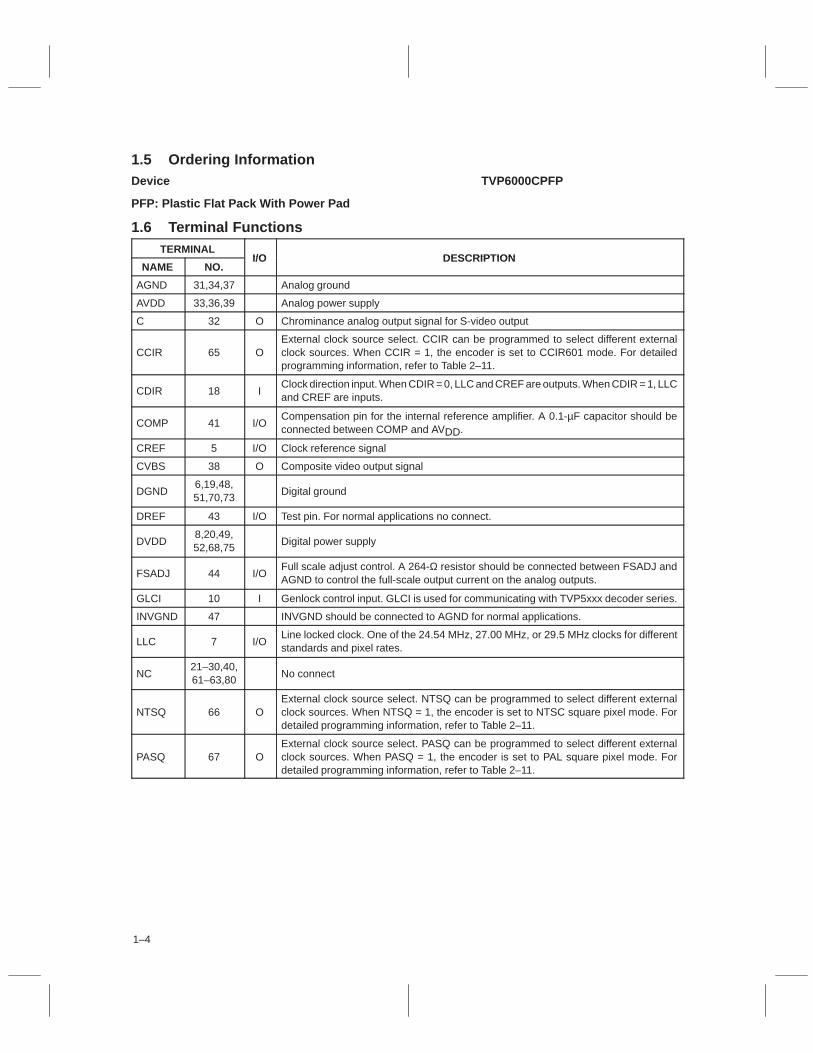
1.6 Terminal FunctionsTERMINAL
I/O DESCRIPTIONNAME NO.
I/O DESCRIPTION
AGND 31,34,37 Analog ground
AVDD 33,36,39 Analog power supply
C 32 O Chrominance analog output signal for S-video output
CCIR 65 OExternal clock source select. CCIR can be programmed to select different externalclock sources. When CCIR = 1, the encoder is set to CCIR601 mode. For detailedprogramming information, refer to Table 2–11.
CDIR 18 IClock direction input. When CDIR = 0, LLC and CREF are outputs. When CDIR = 1, LLCand CREF are inputs.
COMP 41 I/OCompensation pin for the internal reference amplifier. A 0.1-µF capacitor should beconnected between COMP and AVDD.
CREF 5 I/O Clock reference signal
CVBS 38 O Composite video output signal
DGND6,19,48,51,70,73
Digital ground
DREF 43 I/O Test pin. For normal applications no connect.
DVDD8,20,49,52,68,75
Digital power supply
FSADJ 44 I/OFull scale adjust control. A 264-Ω resistor should be connected between FSADJ andAGND to control the full-scale output current on the analog outputs.
GLCI 10 I Genlock control input. GLCI is used for communicating with TVP5xxx decoder series.
INVGND 47 INVGND should be connected to AGND for normal applications.
LLC 7 I/OLine locked clock. One of the 24.54 MHz, 27.00 MHz, or 29.5 MHz clocks for differentstandards and pixel rates.
NC21–30,40,61–63,80
No connect
NTSQ 66 OExternal clock source select. NTSQ can be programmed to select different externalclock sources. When NTSQ = 1, the encoder is set to NTSC square pixel mode. Fordetailed programming information, refer to Table 2–11.
PASQ 67 OExternal clock source select. PASQ can be programmed to select different externalclock sources. When PASQ = 1, the encoder is set to PAL square pixel mode. Fordetailed programming information, refer to Table 2–11.

1–5
1.6 Terminal Functions (Continued)TERMINAL
I/O DESCRIPTIONNAME NO.
I/O DESCRIPTION
RCM1 1 OProgrammable video vertical timing signal. For detailed programming information,see the RCM_L21 register definition.
RCM2 3 I/OProgrammable video horizontal timing signal (can also be programmed for horizontalactive video signal. For detailed programming information, see RCM_L21 registerdefinition.
RCV1 2 I/OProgrammable video vertical timing signal. For programming infromation, seeSYN_CTRL0 register definition.
RCV2 4 I/OProgrammable video horizontal timing signal (can also be programmed for horizontalactive video signal). For detailed programming infromation, see SYN_CTRL0register definition.
VREF 42 I/OTest pin. VREF can be used for bandgap voltage output. For normal operation noconnection.
REFGND 45 Reference ground of output DACs. REFGND should be connected to AGND.
REFVDD 46 Reference power supply of the DACs. REFVDD should be connected to AVDD.
RES 9 I Reset input, active low
SA 15 I I2C slave address select
SCL 16 I/O I2C serial clock input. Maximum clock rate of 400 kHz.
SDA 17 I/O I2C serial data line
SDEN 11 I Test pin. For normal applications connect to DGND.
TST 12 I Test pin. For normal applications connect to DGND.
VP1[7:0]69,71,72,74,76–79
IY input port in 16-bit mode. For 8-bit multiplexed mode, VP1[7:0] is either the YUVmultiplexed port or should be left unconnected based on the FMT(2) register bit.
VP2[7:0] 53–60 IUV input port in 16-bit mode. For 8-bit multiplexed mode, VP2[7:0] is either the YUVmultiplexed port or should be left unconnected based on the FMT(2) register bit.
VSUB 50 VSUB should be connected to AGND.
XDAC 64 IXDAC sets the initial mode of operation for the output DACs immediately after reset. IfXDAC = GND the DACs will be in normal operation mode after reset. If XDAC = VDD,the DACs will be in power down mode.
XTAL1 13 I Crystal or oscillator input. CMOS input levels
XTAL2 14 I Crystal input. Crystal is connected between XTAL1 and XTAL2.
Y 35 O Luminance analog output signal for S-video output

1–6
2–1
2 Detailed DescriptionThe TVP6000 is a digital video encoder designed for systems requiring high-quality display of computergraphics, video, video conferencing, and Internet content. It is designed to convert a digital video input datastream into NTSC or PAL composite video output. Digital input formats include 8 or 16 bit YUV 4:2:2 or 8bit CCIR–656 YUV. Analog output formats are NTSC and PAL.
The encoder provides picture quality enhancement features such as overscan compensation, which allowsup to a 12.5% down scaling of pixels (horizontal) and lines (vertical) to allow fitting a VGA frame on a NTSC.A 3-tap antiflicker filter greatly reduces annoying flicker associated with displaying progressive scangraphics data or text on an interlace display, like TV. The output has simultaneous S-video and compositebaseband video (CVBS) via three 10-bit DACs. Programmable features such as blank levels, color burstamplitude, luminance and chrominance gains, subcarrier frequency, luminance delay allow for easyoptimization of picture quality and subcarrier genlock capability when used with a compatible video decoderprovides accurate color reproduction even with nonstandard or unstable video sources such as a VCR.
See Figure 2–1 for an overview of the major functional blocks of the TVP6000.
2.1 InitializationUpon power up, the TVP6000 is initialized by the internal logic to display a color bar. With this feature, theTVP6000 is able to demonstrate basic functionality while using only a 27-MHz clock signal at the LLC pinor the XTAL1 and XTAL2 crystal pins. No software programming is required for this initial operation. Thisserves as a quick diagnostic tool during the initial debug of a system.
The DACs can also be optionally turned off immediately after reset by connecting the XDAC pin (pin 64) toVDD if the initial color bar display is not desired. In this case, video is not output after reset. See Section 2.11,Register Descriptions for details about the default values immediately after power up.

2–2
Figure 2–1. Block Diagram
Dat
aM
anag
erU
nit
Sca
ling
Pro
cess
or
I2C
Con
trol
Logi
c
Low
Pas
san
dIn
terp
olat
ion
Filt
ers
(5.7
MH
z)
Y
Cr/
Cb
Y UV
Low
Pas
san
dIn
terp
olat
ion
Filt
ers
(1.3
MH
z)
Syn
c. C
lock
Gen
erat
or
+
Clo
sed
Cap
tion
Gen
erat
or
Mod
ulat
oran
dG
ain
Con
trol
sin
sin
cos
SIN
/CO
SL.
U.T
.
Cro
ss C
olor
+10
-Bit
DA
C
10-B
itD
AC
10-B
itD
AC
Y CV
BS
C CO
MP
35 38 32 41
4244
VR
EF
FS
AD
J
Y
Cr/
Cb
69,7
1,72
,74
76–7
9
53–6
0
Y
Cr/
Cb
16 17
SC
L
SD
A
Red
uctio
nF
ilter
2–3
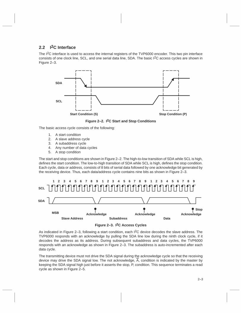
2.2 I2C InterfaceThe I2C interface is used to access the internal registers of the TVP6000 encoder. This two pin interfaceconsists of one clock line, SCL, and one serial data line, SDA. The basic I2C access cycles are shown inFigure 2–3.
Start Condition (S) Stop Condition (P)
SDA
SCL
Figure 2–2. I 2C Start and Stop Conditions
The basic access cycle consists of the following:
1. A start condition2. A slave address cycle3. A subaddress cycle4. Any number of data cycles5. A stop condition
The start and stop conditions are shown in Figure 2–2. The high-to-low transition of SDA while SCL is high,defines the start condition. The low-to-high transition of SDA while SCL is high, defines the stop condition.Each cycle, data or address, consists of 8 bits of serial data followed by one acknowledge bit generated bythe receiving device. Thus, each data/address cycle contains nine bits as shown in Figure 2–3.
SCL
SDA
MSB
Slave Address Subaddress Data
Stop
1 2 3 4 5 6 7 8 9 1 2 3 4 5 6 7 8 9 1 2 3 4 5 6 7 8 9
Acknowledge Acknowledge Acknowledge
Figure 2–3. I 2C Access Cycles
As indicated in Figure 2–3, following a start condition, each I2C device decodes the slave address. TheTVP6000 responds with an acknowledge by pulling the SDA line low during the ninth clock cycle, if itdecodes the address as its address. During subsequent subaddress and data cycles, the TVP6000responds with an acknowledge as shown in Figure 2–3. The subaddress is auto-incremented after eachdata cycle.
The transmitting device must not drive the SDA signal during the acknowledge cycle so that the receivingdevice may drive the SDA signal low. The not acknowledge, A, condition is indicated by the master bykeeping the SDA signal high just before it asserts the stop, P, condition. This sequence terminates a readcycle as shown in Figure 2–5.

2–4
The slave address consists of 7 bits of address along with 1 bit of read/write information as shown inFigures 2–4 and 2–5. For the TVP6000, the possible slave addresses (including the read/write bit) are 0x40or 0x42 for write cycles or 0x41 and 0x43. Refer to Table 2–7 for additional base address information.
S Slave Address W Sub Address A Data A PA Data A
From Transmitter
From Receiver
A = No Acknowledge (SDA High)A = AcknowledgeS = Start ConditionP = Stop ConditionW = Write
Figure 2–4. I 2C Write Cycle
A = No Acknowledge (SDA High)A = AcknowledgeS = Start ConditionP = Stop ConditionW = WriteR = Read
S Slave Address W A PA
TransmitterReceiver
Sub Address
S Slave Address R A PA Data A Data
TransmitterReceiver
Figure 2–5. I 2C Read Cycle
2.3 Data ManagerThe data manager resides at the very beginning of the processing pipeline. It receives the Y Cb Cr pixel datafrom the pixel bus and converts it to its internal YUV representation. Register F_CONTROL at subaddress3A and the SCN bit of the SCM register at subaddress 90 define the function of the data manager.
The data manager can receive data on either an 8-bit or 16-bit video port. In the 8-bit format, it receives dataat port VP1 or VP2 (both 8-bits wide) depending on register bit FMT2, at every rising edge of LLC if scanconversion is disabled, and at every (rising and falling) edge of LLC if scan conversion is enabled. In the16-bit format, it receives luminance information on the VP1 port and chrominance information on the VP2port, at alternate rising edges of LLC (qualified by CREF) if scan conversion is disabled, or at every risingedge of LLC if scan conversion is enabled. Additionally, the data manager can generate pixels internally fora 100/100 color bar if the CBAR bit is set. The Y, U, and V values for this color bar are shown in Table 2–3.

2–5
Table 2–1. 16-Bit Video Port YUV 4:2:2
TIME 0 1 2 3 4 5 6 7
VP1[7:0] Y0 Y1 Y2 Y3
VP2[7:0] Cb0 Cb1 Cb2 Cb3
Luma pixel number 0 1 2 3
Chroma pixel number 0 2
Table 2–2. 8-Bit Multiplexed Video Port CCIR656 YUV 4:2:2
TIME 0 1 2 3 4 5 6 7
VP1[7:0] or VP2[7:0] Cb0 Y0 Cr0 Y1 Cb2 Y2 Cr2 Y3
Luma pixel number 0 1 2 3
Chroma pixel number 0 2
Table 2–3. 100/100 Color Bar in Twos Complement
COLOR Y (hex) Cb (hex) Cr (hex)
White 6B 00 00
Yellow 52 90 12
Cyan 2A 26 90
Green 11 B6 A2
Magenta EA 4A 5E
Red D1 DA 70
Blue A9 70 EE
Black 90 00 00
The SCN bit in the SCM register enables or disables scan conversion. When scan conversion is disabled(SCN = 0), the input scan lines are interlaced at a field rate of 60 Hz for 525-line systems or 50 Hz for 625-linesystems. When scan conversion is enabled (SCN = 1), the input scan lines are non-interlaced at a framerate of 60 Hz or 50 Hz.
2.4 Scaling ProcessorThe scaling processor scales down the input image in both horizontal and vertical directions. In addition toscaling, the scaling processor filters the image in the vertical direction and removes annoying flickers, whichare common when a computer-generated graphics or text, especially a static image, is displayed on TV. Thescaling processor uses a 3-tap adaptive filter, whose coefficients are dynamically adjusted on a line-by-linebasis to maintain optimal performance.
The scaling processor is enabled by setting the SCN register bit to 1. When scan conversion is enabled,the data manager receives non-interlaced pixel data via the demand mode interface and passes pixel dataon to the scaling processor for overscan-compensation processing. The output of the scaling processorfeeds the video encoder core for encoding. See Section 2.5, Video Encoder for a detailed description.
When the scaling processor is disabled, SCN reset to 0, the data manager receives pixel data via masteror slave mode and passes pixel data directly to the video encoder core, bypassing the scaling processor.
The scaling processor, when enabled, is controlled by the following registers: SPPL, DPPL, SLPF, andDLPF. These registers define the size of the image before and after scaling. The SPPL register defines thenumber of active pixels per line before scaling and the DPPL register defines the number of active pixelsper line after scaling. The SLPF register defines the number of active lines before scaling and the DLPFregister defines the number of active lines after scaling. Refer to Section 2.11, Register Descriptions foradditional information on these registers.

2–6
Vertical and horizontal over-scan compensation ratios are independently controlled by two pairs of registers.The VDTAH and VDTAL register pair define the vertical scaling ratio and the HDTAH and HDTAL registerpair define the horizontal scaling ratio. The scaling ratio equations are given in the register descriptionsection. An over-scan compensation ratio up to 12.5% in both vertical and horizontal directions is supported.
When enabled, three modes of vertical scaling and two modes of horizontal scaling are provided for optimalperformance of the target application. For computer graphics and text intensive static images, mode 2vertical scaling (VSC[1:0] = 2) should be used for maximum flicker reduction. For DVD playback, mode 3(VSC[1:0] =3) should be used for sharpness. The nearest neighbor mode is provided only for comparisonand diagnostic purposes, and should not be used for normal applications.
Finally, the scaled image can be placed on the TV screen at a location defined by the VOFS and HOFSregisters. VOFS and HOFS define the location of the upper left corner of the output image. See thedefinitions of the VOFS and HOFS registers for details.
Note that the SWPF bit is provided for test and diagnostic purposes. For normal applications, this bit mustbe set to 0 at all times.
2.5 Video Encoder2.5.1 Luminance Encoding
Programmable gain is first applied to the luminance data output from the data manger or scaling processordepending on whether the TVP6000 is in regular or scan-conversion mode. The luminance gain is definedby the GAIN_Y register at subaddresses 5F and 60. The horizontal sync, vertical sync, and setup insertionare then performed. Both black level and blank level are programmable through the BLACK_LEVEL andBLANK_LEVEL registers at subaddresses 5D and 5E, respectively.
All of the transition edges of the luminance signal such as the sync edges and active video edges areproperly shaped and filtered to limit the bandwidth within the standards.
2.5.2 Luminance Low-Pass and Interpolation Filter
After all of the necessary components of the luminance signal have been added, the resultant signal islow-passed and interpolated to a 2x pixel rate. This 2x interpolation simplifies the external analogreconstruction filter design and improves the signal-to-noise ratio. Refer to Figure 2–6 for the filter frequencyresponse.

2–7
G –
Gai
n –
dB –1
–1.5
–2
–2.5
0 1 2 3 4 5 6
–0.5
0
0.5
7 8 9 10–3
f – Frequency – MHz
NTSC_SQP
PAL_SQPPAL_CCIR/NTSC_CCIR
Figure 2–6. Luma Path Frequency Response
–15
–20
–25
–35
0 1 2 3 4 5 6
G –
Gai
n –
dB
–5
0
f – Frequency – MHz
7 8 9 10–40
–10
–30 NTSC_CCIRNTSC_SQPPAL_SQPPAL_CCIR
Figure 2–7. Luma Cross Color Reduction Filter

2–8
2.5.3 Cross Color Reduction Filter
An optional cross color reduction filter can be applied to the luminance signal before the luminance signalcombines with the chrominance signal to form the composite signal. The cross color reduction filter reducesthe interference between the luminance and chrominance in the composite signal. The cross reduction filterdoes not apply to S-video.
2.5.4 Chrominance Encoding
The time-multiplexed U/V signal is adjusted by a pair of programmable gains. The gain for U and the gainfor V are independently controlled by the GAIN_U and GAIN_V register bits respectively at subaddresses5B, 5C, 5D, and 5E. The gain-adjusted signal then passes through a chrominance low-pass filter to limit thebandwidth of the U/V signal. The chrominance low-pass filter can be optionally bypassed by setting the CBWbit of the M_CONTROL register at subaddress 61 to 0. This setting enlarges the bandwidth on U/V forS-video output.
The low-passed U/V signal is then subjected to a 1-to-4 interpolation through an interpolation filter. The datarate for both U and V is now at a 2x pixel rate.
The U and V signals are then quadrature-modulated by the internally generated subcarrier signal to formthe chrominance (C) signal. The subcarrier reference signal color burst is inserted right before the activevideo.
The frequency, the phase of the modulating subcarrier, and the amplitude of the color burst are allprogrammable. When genlock is disabled (the GLCE bit of the M_CONTROL register set to 0), thesubcarrier frequency is controlled by the S_CARR registers at subaddresses 63, 64, 65, and 66. The valuesof the registers are computed based on the desired subcarrier frequency and the LLC clock using theequation in the register description. Table 2–12 lists the most commonly used values for various standards.When genlock is enabled (GLCE set to 1), the subcarrier frequency is updated once every scan line usingthe frequency control bits serially shifted in at the GLCI pin.
The C_PHASE register at subaddress 5A controls the phase of the subcarrier. The phase of the colorsubcarrier is reset to C_PHASE when enabled. Four modes of color subcarrier reset are provided: resetevery two lines, every two fields, every eight fields, or at a reset bit input at the GLCI pin if genlock is enabled.Users can use the C_PHASE register to adjust the subcarrier-to-horizontal sync phase. The bits BSTAP[6:0]of the BSTAMP register at subaddress 62 sets the amplitude of the color burst. The PAL bit of theM_CONTROL register enables phase alternation line encoding. A sweeping subcarrier is generated toencode the chrominance signal when the PAL bit is set to 1. Otherwise a normal subcarrier is generated.Phase alternation line refers to an encoding scheme in which the subcarrier alternates between two differentphases every scan line. There are two possible alternate sequences and the PALPHS bit of theM_CONTROL register selects one of the sequences.
2–9
–30
–40
–50
–60
0 0.5 1 1.5 2 2.5 3
G –
Gai
n –
dB
–20
–10
f – Frequency – MHz
0
3.5 4 4.5 5
NTSC_SQPPAL_SQPPAL_CCIR/NTSC_CCIR
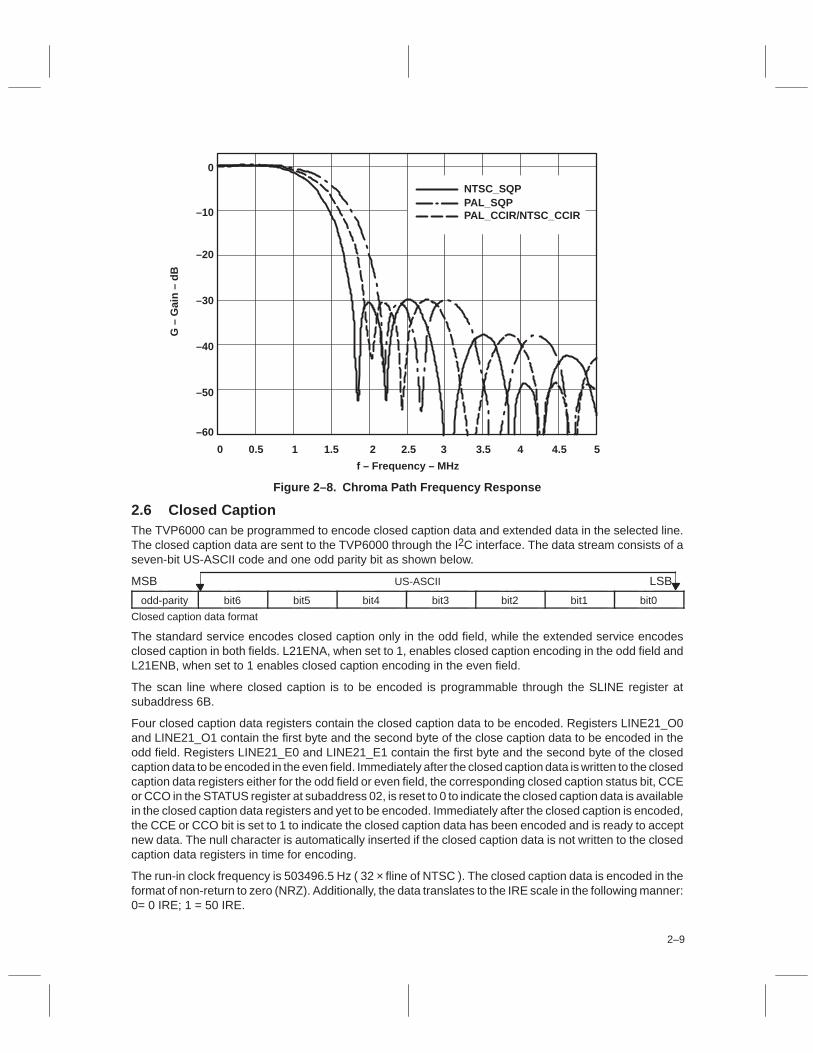
Figure 2–8. Chroma Path Frequency Response
2.6 Closed CaptionThe TVP6000 can be programmed to encode closed caption data and extended data in the selected line.The closed caption data are sent to the TVP6000 through the I2C interface. The data stream consists of aseven-bit US-ASCII code and one odd parity bit as shown below.
MSB US-ASCII LSB
odd-parity bit6 bit5 bit4 bit3 bit2 bit1 bit0
Closed caption data format
The standard service encodes closed caption only in the odd field, while the extended service encodesclosed caption in both fields. L21ENA, when set to 1, enables closed caption encoding in the odd field andL21ENB, when set to 1 enables closed caption encoding in the even field.
The scan line where closed caption is to be encoded is programmable through the SLINE register atsubaddress 6B.
Four closed caption data registers contain the closed caption data to be encoded. Registers LINE21_O0and LINE21_O1 contain the first byte and the second byte of the close caption data to be encoded in theodd field. Registers LINE21_E0 and LINE21_E1 contain the first byte and the second byte of the closedcaption data to be encoded in the even field. Immediately after the closed caption data is written to the closedcaption data registers either for the odd field or even field, the corresponding closed caption status bit, CCEor CCO in the STATUS register at subaddress 02, is reset to 0 to indicate the closed caption data is availablein the closed caption data registers and yet to be encoded. Immediately after the closed caption is encoded,the CCE or CCO bit is set to 1 to indicate the closed caption data has been encoded and is ready to acceptnew data. The null character is automatically inserted if the closed caption data is not written to the closedcaption data registers in time for encoding.
The run-in clock frequency is 503496.5 Hz ( 32 × fline of NTSC ). The closed caption data is encoded in theformat of non-return to zero (NRZ). Additionally, the data translates to the IRE scale in the following manner:0= 0 IRE; 1 = 50 IRE.
2–10
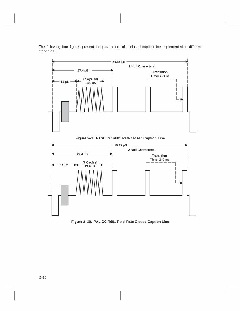
The following four figures present the parameters of a closed caption line implemented in differentstandards.
10 µS(7 Cycles)
13.9 µS
27.4 µS TransitionTime: 220 ns
2 Null Characters59.65 µS
Figure 2–9. NTSC CCIR601 Rate Closed Caption Line
10 µS(7 Cycles)
13.9 µS
27.4 µS TransitionTime: 240 ns
2 Null Characters59.67 µS
Figure 2–10. PAL CCIR601 Pixel Rate Closed Caption Line

2–11
10 µS(7 Cycles)
13.9 µS
27.4 µS TransitionTime: 200 ns
2 Null Characters59.67 µS
Figure 2–11. NTSC Square Pixel Rate Closed Caption Line
10.2 µS(7 Cycles)
13.9 µS
27.5 µS TransitionTime: 200 ns
2 Null Characters61.2 µS
Figure 2–12. PAL Square Pixel Rate Closed Caption Line
2.7 Clock GenerationWhen the CDIR pin is tied low, the TVP6000 generates the clock from the crystal connected between XTAL1and XTAL2. Optionally, an oscillator connected to XTAL1 can also be used. The clock is used internally andis also properly buffered and output at the LLC pin. The clock qualifying reference signal, CREF, is also anoutput in this mode.
When CDIR is tied high, the LLC and CREF pins are inputs. The TVP6000 receives the clock signal fromthe LLC pin and the clock qualifying reference signal from the CREF pin.
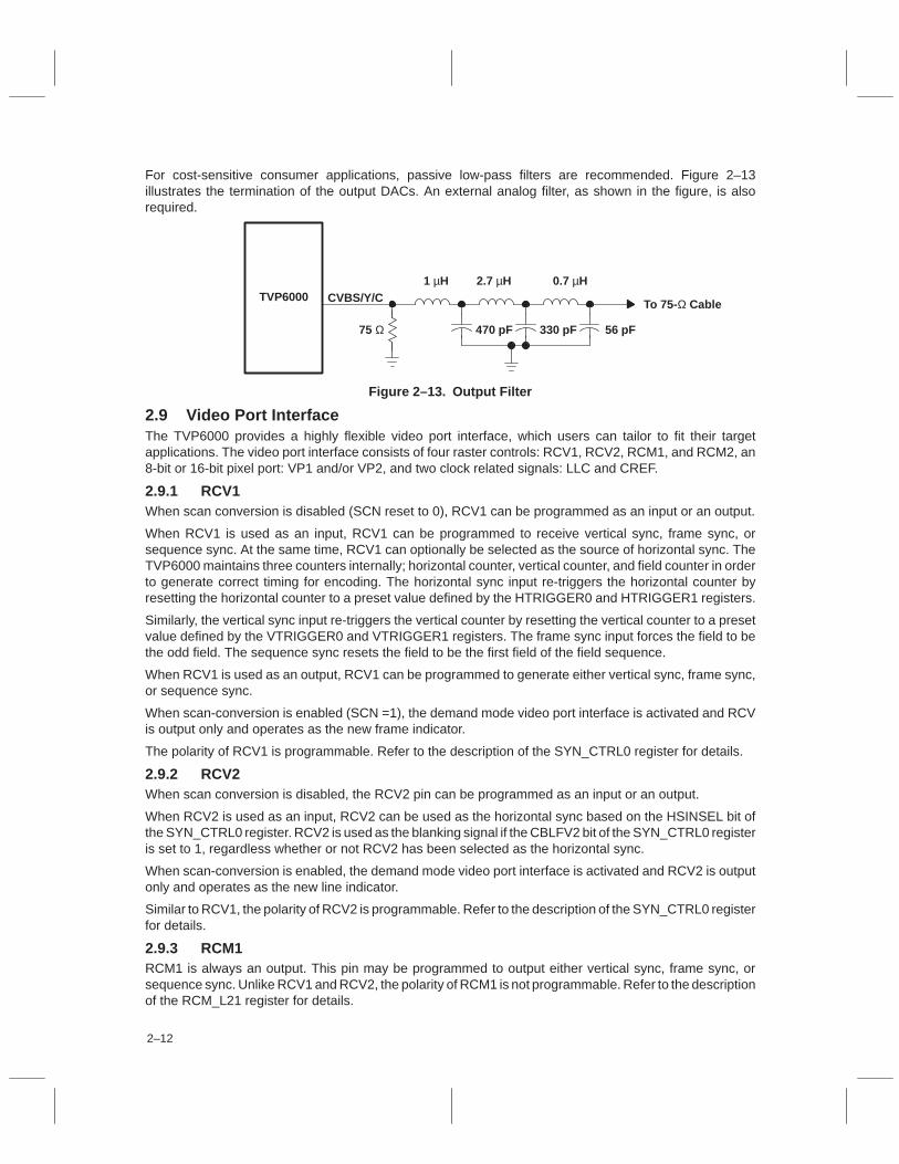
2.8 Analog OutputThe TVP6000 supports simultaneous composite and S-video outputs. Additionally, the DACs may beindependently turned off via software to minimize power dissipation.
The output DACs are current sources and are optimal for driving a 37.5-Ω load with double 75-Ω termination.A 264-Ω full-scale adjust resistor must be connected between the FSADJ pin and ground.
2–12
For cost-sensitive consumer applications, passive low-pass filters are recommended. Figure 2–13illustrates the termination of the output DACs. An external analog filter, as shown in the figure, is alsorequired.
To 75-Ω CableCVBS/Y/C
75 Ω
TVP60001 µH 2.7 µH 0.7 µH
470 pF 330 pF 56 pF
Figure 2–13. Output Filter
2.9 Video Port InterfaceThe TVP6000 provides a highly flexible video port interface, which users can tailor to fit their targetapplications. The video port interface consists of four raster controls: RCV1, RCV2, RCM1, and RCM2, an8-bit or 16-bit pixel port: VP1 and/or VP2, and two clock related signals: LLC and CREF.
2.9.1 RCV1When scan conversion is disabled (SCN reset to 0), RCV1 can be programmed as an input or an output.
When RCV1 is used as an input, RCV1 can be programmed to receive vertical sync, frame sync, orsequence sync. At the same time, RCV1 can optionally be selected as the source of horizontal sync. TheTVP6000 maintains three counters internally; horizontal counter, vertical counter, and field counter in orderto generate correct timing for encoding. The horizontal sync input re-triggers the horizontal counter byresetting the horizontal counter to a preset value defined by the HTRIGGER0 and HTRIGGER1 registers.
Similarly, the vertical sync input re-triggers the vertical counter by resetting the vertical counter to a presetvalue defined by the VTRIGGER0 and VTRIGGER1 registers. The frame sync input forces the field to bethe odd field. The sequence sync resets the field to be the first field of the field sequence.
When RCV1 is used as an output, RCV1 can be programmed to generate either vertical sync, frame sync,or sequence sync.
When scan-conversion is enabled (SCN =1), the demand mode video port interface is activated and RCVis output only and operates as the new frame indicator.
The polarity of RCV1 is programmable. Refer to the description of the SYN_CTRL0 register for details.
2.9.2 RCV2When scan conversion is disabled, the RCV2 pin can be programmed as an input or an output.
When RCV2 is used as an input, RCV2 can be used as the horizontal sync based on the HSINSEL bit ofthe SYN_CTRL0 register. RCV2 is used as the blanking signal if the CBLFV2 bit of the SYN_CTRL0 registeris set to 1, regardless whether or not RCV2 has been selected as the horizontal sync.
When scan-conversion is enabled, the demand mode video port interface is activated and RCV2 is outputonly and operates as the new line indicator.
Similar to RCV1, the polarity of RCV2 is programmable. Refer to the description of the SYN_CTRL0 registerfor details.
2.9.3 RCM1RCM1 is always an output. This pin may be programmed to output either vertical sync, frame sync, orsequence sync. Unlike RCV1 and RCV2, the polarity of RCM1 is not programmable. Refer to the descriptionof the RCM_L21 register for details.

2–13
2.9.4 RCM2The RCM2 pin may be configured as an input or an output as shown in Table 2–19. The polarity of the RCM2pin is programmable via this register as well.
As an output, this pin may be operated as a horizontal sync, composite blank, or a demand mode datarequest signal. As in input, this pin is always a composite blanking input.
When scan-conversion is enabled, the demand mode video port interface is activated and the RCM2 pinacts as the request output pin.
2.10 Modes of OperationWith a highly programmable video port interface, the TVP6000 may be configured to operate in variousmodes, each tailored for a target application. In the following sections, several of the most commonly usedmodes are described.
2.10.1 Master ModeIn the master mode, the TVP6000 generates all of the video timing signals for controlling an externalgraphics controller or MPEG decoder device. Table 2–4 lists the timing signals that are output from theTVP6000 during master mode.
Table 2–4. Master Mode
PIN NAME I/O TYPE DESCRIPTION
LLC Input/output Line locked clock; with 2X pixel clock frequency.
CREF Input/output Data phase reference clock.
RCM1 Output Output vertical/field timing, can be programmed as VSO/FSO/FSEQO
RCV1 Output Output vertical/field timing, can be programmed as VSO/FSO/FSEQO
RCM2 OutputOutput horizontal timing, programmed as CBNO. Active duration is definedby registers BMRQ and EMRQ, excluding vertical blanking interval.
RCV2 OutputOutput horizontal timing, programmed as HSO. Active duration is definedby registers BRCV and ERCV.
Refer to Table 2–15 and Table 2–17 for the definitions of VSO, FSO, FSEQO, and HSO.
A crystal with the correct frequency according to Table 2–5 should be connected between pins XTAL1 andXTAL2.
Table 2–5. Crystal Frequencies
PIXEL RATE CLOCK FREQUENCY
CCIR-601 27 MHz 27 MHz
Square pixel 24.5454 MHz 29.5 MHz
2.10.2 Slave ModeIn slave mode, all clock and video timing signals are supplied from an external source. The source may bea graphics controller, an MPEG device, or a TV decoder such as the TVP5010/TVP5020 decoders.Table 2–6 lists the signal definitions for slave mode.

2–14
Table 2–6. Slave Mode Signals
PIN NAME I/O TYPE DESCRIPTION
LLC Input Line locked clock with 2X pixel clock frequency. CDIR pin is tied high.
CREF Input Data phase reference clock. CDIR pin is tied high.
RCM1 Output Output Vertical/Field timing, can be programmed as VSO/FSO/FSEQO
RCV1 Input Can be programmed as VSI/FSI/FSEQI.
RCM2 Input Programmed as CBNI.
RCV2 Input Programmed as HSI.
Refer to Table 2–15 and Table 2–17 for the definition of VSO, FSO, FSEQO, HSO, VSI, FSI, FSEQI, CBNI,and HSI.
2.10.3 Demand Mode
Demand mode is an interface specially designed for scan conversion. When scan conversion is enabled,the TVP6000 accepts non-interlaced pixel data, performs signal processing functions which includenon-interlace-to-interlace conversion, flicker filtering and overscan-compensation, and outputs interlacedNTSC/PAL video. Due to the nature of the functions that the TVP6000 performs during scan conversion,the bandwidth of the input pixel increases and exceeds what the master and slave mode interface canprovide. Demand mode provides extra bandwidth to meet the needs of the TVP6000.
Unlike master mode and slave mode, the video port interface timing for demand mode is decoupled fromthe timing of the internal encoder core.
The TVP6000 operates in demand mode when it requests data from an external graphics controller or anMPEG device. Demand mode is enabled by setting SCM[0] = 1, the SCN bit.
In demand mode, the TVP6000 asserts the RCM2 pin high to request additional data from the externalsource and negates the RCM2 pin to stop additional data transfer. Table 2–19 shows how the RCM2 pinmay be programmed to operate as a request signal during demand mode. In addition, the NLR register isused to program the threshold where the RCM2 pin is toggled for requests.
2.10.4 Genlock Mode
The TVP6000 may be configured in a genlock mode to an external TV decoder such as theTVP5000/TVP5010 device. This configuration allows the decoder to drive video timing information to theTVP6000 encoder. The genlock mode is used to control clock jitter and thus allows the encoder to generateaccurate color burst information.
In this configuration, GLCI pin is connected to the GLCO pin of the decoder, and the line-lock clock pin, LLC,is fed by the decoder main pixel clock output. Moreover, the color sub-carrier information is formatted asa 23-bit binary number and is transmitted serially. The transmission timing diagram is shown in Figure 2–13.

2–15
SCLK
GLCO
>128 LLCs
MSB LSB
Inactive
Start Bit 0
1 LLC 23 LLCs
23-Bit DTO Frequency Control Inactive
7 LLCs 1 LLC
Sub Carrier DTO Phase Reset
Where DTO = Discrete Time Oscillator
Figure 2–14. Transmission Timing
2.11 Register DescriptionsThe TVP6000 is a standard I2C slave device. All of the registers can be written and read through the I2Cinterface. The I2C base addresses of the TVP6000 are dependent on pin 15 (SA) as listed in Table 2–7.
Table 2–7. Base Addresses
PIN 15 WRITE ADDRESS(hex)
READ ADDRESS (hex)
0 40 41
1 42 43
Table 2–8. Register Bit Allocation Map
REGISTER R/WSUB-
ADDRESS BIT7 BIT6 BIT5 BIT4 BIT3 BIT2 BIT1 BIT0
DEV_ID R 00 Dev id[7:0]
REV_ID R 01 Rev id[7:0]
STATUS R 02 Scon Ccon Cce Cco Fsq[2:0]
Reserved 03–39 Reserved
F_CONTROL R/W 3A Cbar Fmt2 Y2c Uv2c Fmt[1:0]
Reserved 3B–59 Reserved
C_PHASE R/W 5A Cphase[7:0]
GAIN_U R/W 5B Gu[7:0]
GAIN_V R/W 5C Gv[7:0]
BLACK_LEVEL R/W 5D Gu8 Black[6:0]
BLANK_LEVEL R/W 5E Gv8 Blank[6:0]
GAIN_Y R/W 5F Gy[7:0]
X_COLOR R/W 60 0 Xc Gy8 Lcd[2:0]
M_CONTROL R/W 61 Sdown Cdown Palphs 0 Glce Cbw Pal Ffrq
BSTAMP R/W 62 Sqp Bstap[6:0]
S_CARR1 R/W 63 Fsc[7:0]
S_CARR2 R/W 64 Fsc[15:8]
S_CARR3 R/W 65 Fsc[23:16]
S_CARR4 R/W 66 Fsc[31:24]
LINE21_O0 R/W 67 L21o[7:0]
LINE21_O1 R/W 68 L21o[15:8]

2–16
Table 2–8. Register Bit Allocation Map (Continued)
REGISTER R/WSUB-
ADDRESS BIT7 BIT6 BIT5 BIT4 BIT3 BIT2 BIT1 BIT0
LINE21_E0 R/W 69 L21e[7:0]
LINE21_E1 R/W 6A L21e[15:0]
LN_SEL R/W 6B Sline[4:0]
SYN_CTRL0 R/W 6C Rcv1a Rcv1b Hsinel Orcv1 Prcv1 Cblfv2 Orcv2 Prcv2
RCML21 R/W 6D Crcm2 Cblfm2 Orcm2 Prcm2 Rcm1a Rcm1b L21ena L21enb
HTRIGGER0 R/W 6E htrig[7:0]
HTRIGGER1 R/W 6F Htrig[10:8]
VTRIGGER R/W 70 Presa Presb Sblank Vtrig[4:0]
BMRQ R/W 71 Bmrq[7:0]
EMRQ R/W 72 Emrq[7:0]
BEMRQ R/W 73 Emrq[10:8] Bmrq[10:8]
RESERVED 74–76 Reserved
BRCV R/W 77 Brcv[7:0]
ERCV R/W 78 Ercv[7:0]
BERCV R/W 79 Ercv[10:8] Brcv[10:8]
FLEN R/W 7A Flen[7:0]
FAL R/W 7B Fal[7:0]
LAL R/W 7C Lal[7:0]
FLAL R/W 7D Lal8 Fal8 Flen[9:8]
SYN_CTRL1 R/W 7E Esav Ignp Free Blnks Avm[1:0]
RESERVED 7F Reserved
SCM R/W 90 Swpf Hsc[1:0] Vsc[1:0] Scn
SLPF R/W 91 Slpf[7:0]
SPPL R/W 92 Sppl[7:0]
SLPH R/W 93 Sppl[9:8] Slpf[9:8]
DLPF R/W 94 Dlpf[7:0]
DPPL R/W 95 Dppl[7:0]
DLPH R/W 96 Dppl[9:8] Dlpf[9:8]
VDTAL R/W 97 Vdta[7:0]
VDTAH R/W 98 Vdta[15:8]
HDTAL R/W 99 Hdta[7:0]
HDTAH R/W 9A Hdta[15:8]
VOFS R/W 9B Vofs[7:0]
HOFS R/W 9C Hofs[7:0]
NLR R/W 9D Nlr[7:0]
TEST1 R/W 9E
TEST2 R/W 9F
TEST3 R/W A0
RESERVED A1–FF Reserved

2–17
2.11.1 DEV_ID
Subaddress:00 (Read Only) Default: 0x60
7 6 5 4 3 2 1 0
Dev_ID[7:0]
This read only register contains the device ID for the TVP6000. The 8-bit device ID for the TVP6000 is 0x60.
2.11.2 REV_ID
Subaddress:01 (Read Only) Default: 0x00
7 6 5 4 3 2 1 8
Rev_ID[7:0]
This read only register contains the revision ID for the TVP6000. The revision ID identifies different revisionsof the device.
2.11.3 STATUS
Subaddress:02 (Read Only)
7 6 5 4 3 2 1 0
SCON CCON CCE CCO FSQ[2:0]
Where:SCON S-video connection status
0 Not connected1 Connected
CCON Composite video connection status0 Not connected1 Connected
CCE Closed-caption status bit for even field. This bit is set immediately after the data inregisters LINE21_E0 and LINE21_E1 has been encoded to closed caption. This bit isreset when both of these registers are written.
CCO Closed-caption status bit for odd field. This bit is set immediately after the data inregisters LINE21_O0 and LINE21_O1 has been encoded to closed caption. This bit isreset when both of these registers are written.
FSQ[2:0] Field sequence ID. For PAL, all three bits FSQ[2:0] are used whereas for NTSC onlybits FSQ[1:0] are meaningful. Futhermore, FSQ(0) represents the odd field when it is a0 and the even field when it is 1.

2–18
2.11.4 F_CONTROL
Subaddress:3A Default: 0x8D
7 6 5 4 3 2 1 0
CBAR FTM[2] Y2C UV2C FTM[1:0]
Format control register. This register specifies the input video source and format.Where:
CBAR Select video data source0 Use external video source1 Use internal color bars
Y2C Y data format selection0 The input Y data are in twos complement format1 The input Y data are in binary format
UV2C CrCb data format selection0 The input CrCb data is in twos complement format1 The inputCrCb data is in binary format
FTM[2:0] These three bits detemine the video input data stream format and timing as listedin Table 2–9. The SCN bit (subaddress 90, bit 0) is also used in this decode.
Table 2–9. Input Format and Data Sampling
SCN FTM[2:0] INPUT FORMAT SAMPLING TIMEINTERNALENCODER
CLOCK
0 X 0 0 Reserved Reserved Reserved
0 X 0 1 YUV 4:2:2 on VP1 and VP2Data is sampled at the rising edge of LLCqualified by CREF.
LLC
0 0 1 0 YUV 4:2:2 on VP1 port Data is sampled at the rising edge of LLC LLC
0 1 1 0 YUV 4:2:2 on VP2 port Data is sampled at the rising edge of LLC LLC
0 0 1 1 CCIR 656 on VP1 port Data is sampled at the rising edge of LLC LLC
0 1 1 1 CCIR 656 on VP2 port Data is sampled at the rising edge of LLC LLC
1 X 0 0 Reserved Reserved Reserved
1 X 0 1 YUV 4:2:2 Data is sampled at the rising edge of LLC LLC
1 0 1 0 YUV 4:2:2 on VP1 port Data is sampled at both edges of LLC LLC
1 1 1 0 YUV 4:2:2 on VP2 port Data is sampled at both edges of LLC LLC
1 X 1 1 Reserved

2–19
2.11.5 C_PHASE
Subaddress: 5A Default: 0x00
7 6 5 4 3 2 1 0
CPHS[7:0]
Where:
CPHS[7:0] Phase of encoded video color subcarrier (including the color burst) relative toHsync. The adjustable step is 360/256.
2.11.6 GAIN_U
Subaddress: 5B Default: 0x01
7 6 5 4 3 2 1 0
GU[7:0]
Where:GU[7:0] Gain control of Cb signal. The MSB, GU8, is located at subaddress 5D, bit 7.
In the case of NTSC with a 7.5 IRE pedestal, WHITE – BLACK = 92.5 IREGain_U= 0x101.In the case of no pedestal (PAL/SECAM), WHITE – BLACK = 100 IRE.Gain_U = 0x115.
2.11.7 GAIN_V
Subaddress: 5C Default: 0x6B
7 6 5 4 3 2 1 0
GV[7:0]
Where:
GV[7:0] Gain control of Cr signal. The MSB, GV8 is located at subaddress 5E, bit 7.In the case of NTSC with a 7.5 IRE pedestal, WHITE – BLACK = 92.5 IRE.Gain_V = 0x16B.In the case of no pedestal (PAL/SECAM), WHITE – BLACK = 100 IRE.Gain_V = 0x18C.
2.11.8 BLACK_LEVEL
Subaddress: 5D Default: 0xCC
7 6 5 4 3 2 1 0
GU8 BLACK[6:0]
Where:GU8 The most significant bit of the GAIN_U register. See the GAIN_U register for more
information.BLACK[6:0]Black level setting for NTSC = 0x4C and for PAL = 0x3C.
2–20
2.11.9 BLANK_LEVEL
Subaddress: 5E Default: 0xB8
7 6 5 4 3 2 1 0
GV8 BLANK[6:0]
Where:GV8 The most significant bit of the GAIN_V register. See the GAIN_V register for more
information.BLANK[6:0]Blank level setting for NTSC = 0x38 and for PAL = 0x3C.
2.11.10 GAIN_Y
Subaddress: 5F Default: 0x2E
7 6 5 4 3 2 1 0
GY(7–0)
Where:
GY[7:0] Gain control of Y signal. The MSB, bit 8, is located at subaddress 60, bit 5.In the case of NTSC with a 7.5 IRE pedestal, WHITE – BLACK = 92.5 IRE.Gain_Y = 0x12EIn the case of no pedestal (PAL/SECAM), WHITE – BLACK = 100 IRE.Gain_Y = 0x145
2.11.11 X_COLOR
Subaddress: 60 Default: 0x20
7 6 5 4 3 2 1 0
XC GY8 LCD(2–0)
Cross color and chroma delay compensation register
Where:XC Cross color reduction enable for composite video output. Cross color does not affect
S-video output0 Cross color reduction is disabled (default)1 Cross color reduction is enabled
GY8 MSB of Gain_Y register.LCD[2:0] These three bits can be used for chroma channel delay compensation during S-video
mode. Table 2–10 shows the delay corresponding to the LCD[2:0] settings.
Table 2–10. Chroma Channel Delays
LCD[2:0]DELAY ON CHROMA
CHANNEL
0 0 0 0
0 0 1 0.5 pixel clock period
0 1 0 1 pixel clock period
0 1 1 1.5 pixel clock period
1 x x 2 pixel clock period

2–21
2.11.12 M_CONTROLSubaddress: 61 Default: 0x05
7 6 5 4 3 2 1 0
SDOWN CDOWN PALPHS GLCE CBW PAL FFRQ
Mode control register. This register provides various operating mode controls including DAC powermanagement.
Where:SDOWN S-video DAC power down
0 Normal operation (default)1 Power down mode
CDOWN Composite video DAC power down0 Normal operation (default)1 Power down mode
PALPHS PAL switch phase setting0 PAL switch phase is nominal (default)1 PAL switch phase is inverted compared to nominal
GLCE Genlock control enable. See Table 2–20.0 No genlock to the color subcarrier frequency (default)1 Genlock-to-color subcarrier frequency is from the TVP5010
CBW Chrominance encoding bandwidth enlarge enable0 Bandwidth for chrominance encoding is enlarged1 Standard bandwidth for chrominance encoding (default)
PAL Phase alternation line encoding selection0 Phase alternation line encoding disabled (default)1 Phase alternation line encoding enabled
FFRQ Field rate selection. Refer to Table 2–11 for programming information.0 50 Hz1 60 Hz (default)
2.11.13 BSTAMPSubaddress: 62 Default:0x38
7 6 5 4 3 2 1 0
SQP BSTAP[6:0]
Color burst amplitude
Where:SQP Square-pixel sampling rate. Refer to Table 2–11 for programming information.
0 CCIR601 sampling rate1 Square-pixel sampling rate
BSTAP[6:0] Setting of the amplitude of color burst. The value for NTSC = 0x38 and forPAL = 0x41.
The SQP and FFRQ bits control the total number of horizontal pixels displayed per scan line. In addition,these bits control the CCIR, NTSQ, and PASQ status pins as shown in Table 2–11.

2–22
Table 2–11. Total Horizontal Pixel Selection
MODE SQP FFRQ CCIR NTSQ PASQ NUMBER OF PIXELS PER LINE
CCIR601 PAL 0 0 high low low 864
CCIR601 NTSC 0 1 high low low 858
Square pixel PAL 1 0 low low high 944
Square pixel NTSC 1 1 low high low 780
2.11.14 S_CARR1, 2, 3, 4
Subaddress: 63, 64, 65, 66 Default: 0xF6, 0x7B, 0xF0, 0x21
7 6 5 4 3 2 1 0
FSC07 FSC06 FSC05 FSC04 FSC03 FSC02 FSC01 FSC00
FSC15 FSC14 FSC13 FSC12 FSC11 FSC10 FSC09 FSC08
FSC23 FSC22 FSC21 FSC20 FSC19 FSC18 FSC17 FSC16
FSC31 FSC30 FSC29 FSC28 FSC27 FSC26 FSC25 FSC24
Color subcarrier frequency registers
Where:FSC[31:0] These four bytes of data are used to program the color subcarrier frequency. These
four bytes are determined by the following formula. S_carr = ROUND((Fsc/Fclock) × 232)
Table 2–12 lists some common values for S_CARR.
Table 2–12. S_CARR Values
STANDARDPIXELTYPE
SUBCARRIERFREQUENCY (fsc)
CLOCK(fclock) S_CARR (dec) S_CARR (hex)
M/NTSC Rectangular 3.579545 MHz 27 MHz 569408543 (default) 21F07C1F
B, D, G, H, I, N/PAL Rectangular 4.43361875 MHz 27 MHz 705268427 2A098ACB
N/PAL(combination N/PAL)
Rectangular 3.58205625 MHz 27 MHz 569807942 21F69446
M/PAL Rectangular 3.5756083125 MHz 27 MHz 568782819 21E6EFE3
M/NTSC Square 3.579545 MHz 24.5454 MHz 626349397 25555555
B, D, G, H, I, N/PAL Square 4.43361875 MHz 29.5 MHz 645499916 26798C0C
N/PAL(combination N/PAL)
Square 3.58205625 MHz 29.5 MHz 521519134 1F15C01E
Combinational N Square 3.5756083125 MHz 24.5454 MHz 625661101 254AD4AD

2–23
2.11.15 LINE21_O0
Subaddress: 67
7 6 5 4 3 2 1 0
L21O[7:0]
Where:L21O[7:0] Least significant byte of of closed caption data in odd field.
Initial value is undefined.
2.11.16 LINE21_O1
Subaddress: 68
7 6 5 4 3 2 1 0
L21O[15:8]
Where:L21O[15:8] Most significant byte of closed caption data in odd field.
Initial value is undefined.
2.11.17 LINE21_E0
Subaddress: 69
7 6 5 4 3 2 1 0
L21E[7:0]
Where:L21E[7:0] Least significant byte of extended service data in even field.
2.11.18 LINE21_E1
Subaddress: 6A
7 6 5 4 3 2 1 0
L21E[15:8]
Where:L21E[15:08] Most significant byte of extended service data in even field.
2.11.19 LN_SEL
Subaddress: 6B
7 6 5 4 3 2 1 0
SLINE[4:0]
Where:SLINE[4:0] Selects the line where closed caption or extended service data are encoded.

2–24
2.11.20 SYN_CTRL0
Subaddress: 6C Default: 0x00
7 6 5 4 3 2 1 0
RCV1A RCV1B HINSEL ORCV1 PRCV1 CBLFV2 ORCV2 PRCV2
This register provides I/O control and the functional definition for the RCV1 and RCV2 pins.
Where:RCV1A This bit along with the RCV1B, SCN (bit 0, subaddress 90) define the signal type on
pin RCV1. See Table 2–13 and Table 2–14.RCV1B This bit along with the RCV1A, SCN (bit 0, subaddress 90) define the signal type on
pin RCV1. See Table 2–13 and Table 2–14.HSINSEL Horizontal synchronization input selection
0 RCV1 pin is the Hsync input1 RCV2 pin is the Hsync input
ORCV1 Output RCV10 RCV1 is set as an input pin1 RCV1 is set as an output pin
PRCV1 Polarity setting of RCV10 RCV1 is active high when it is set as an output, the rising edge is the
active edge when it is set as an input.1 RCV1 is active low when it is set as an output, the falling edge is the
active edge when it is set as an input.CBLFV2 Composite blanking output on RCV2. This bit combined with the SCN bit (bit 0,
subaddress 90), CBLFV2 (bit 2, subaddress 6C), and HSINSEL bits (bit 5,subaddress 6C) define the signal type on RCV2. See Table 2–16 forprogramming information.
ORCV2 Output RCV20 RCV2 is set as an input pin1 RCV2 is set as an output pin
PRCV2 Polarity setting of RCV20 RCV2 polarity is active high. The rising edge of RCV2 is the active edge.1 RCV2 polarity is active low. The falling edge of RCV2 is the active edge.

2–25
The RCV1 pin configurations are listed in Table 2–13.
Table 2–13. RCV1 Pin Configurations
SCN RCV1A RCV1B HSINSELRCV1 PIN
SCN RCV1A RCV1B HSINSELAS OUTPUT AS INPUT
0 0 0 0 VSO Unused
0 0 0 1 VSO VSI
0 0 1 0 FSO HSI and FSI
0 0 1 1 FSO FSI
0 1 0 0 FSEQO HSI and FSEQI
0 1 0 1 FSEQO FSEQI
0 1 1 X Reserved Reserved
1 X X X NFO Reserved
The RCV1 symbols and signal descriptions are listed in Table 2–14.
Table 2–14. RCV1 Symbols and Signal Descriptions
SYMBOL SIGNAL DESCRIPTION
VSO Field synchronization output. Active once every field during vertical sync period. For NTSC, VS = 3 lines,for PAL, VS = 2.5 lines.
VSI Vertical synchronization input. Retriggers the vertical counter. The active edge in the first half of the scanline resets the vertical counter to VTRIG.
FSO Frame synchronization output. Active in the odd field (first field). Inactive in the even field (second field).
FSEQO Field sequence. For NTSC (bit 0, subaddress 61 set to 1), active only in the first field of every four fields. ForPAL (bit 0, subaddress 61 reset to 0), active only in the first field of every eight fields.
NFO New frame indicator output. In scan conversion mode (SCN set to 1), the active edge of this signalindicates to external logic to advance to the next frame.
HSO Horizontal synchronization output.
HSI Horizontal synchronization input. Retriggers the horizontal counter.
FSI Frame synchronization input. Retriggers the vertical counter and resets the field to odd.
FSEQI Field sequence input. Retriggers the vertical counter and resets the field to the first of four fields for NTSCor the first of eight fields for PAL.
The RCV2 pin configurations are listed in Table 2–15.
Table 2–15. RCV2 Pin Configurations
SCN CBLFV2 HSINSEL RCV2 PIN
AS OUTPUT AS INPUT
0 0 0 HSO No function
0 0 1 HSO HSI
0 1 0 CBNO CBNI
0 1 1 CBNO HSI and CBNI
1 X X NLO Reserved

2–26
The RCV2 symbols and signal descriptions are listed in Table 2–16.
Table 2–16. RCV2 Symbols and Signal Descriptions
SYMBOL SIGNAL DESCRIPTION
HSO Horizontal synchronization output. As an output, RCV2 is asserted between BRCV and ERCV in every lineincluding VBI.
HSI As an input, RCV2 is used for horizontal synchronization. Retriggers the horizontal counter.
CBNO As an output, RCV2 is asserted between BRCV and ERCV from line FAL to LAL excluding VBI.
CBNI As an input, RCV2 is used for composite blanking.
NLO Output only, RCV2 generates a 4 LLC clock wide new line indicator at the beginning of a line to indicate tothe external logic to advance to the next line.
2.11.21 RCM_L21
Subadress: 6D Deault: 0x00
7 6 5 4 3 2 1 0
CRCM2 CBLFM2 ORCM2 PRCM2 RCM1A RCM1B L21ENA L21ENB
Where:CRCM2 CREF modulation enable
0 CREF modulation is disabled1 CREF modulation is enabledWhen RCM2 is programmed as an active video output (ORCM2 = 1), CREFmodulation is enabled (CRCM2 = 1), and a 16-bit video input port is used, RCM2is modulated by the internal CREF signal. The modulation is performedbefore polarity control.
CBLFM2 See Table 2–18 for programming information.ORCM2 I/O setting of RCM2
0 RCM2 is set as an input pin (default). 1 RCM2 is set as an output pin.
PRCM2 Polarity setting of RCM20 RCM2 polarity is active high (default).1 RCM2 polarity is active low.
RCM1A Determines which signal is output to pin RCM1. Refer to Table 2–17.RCM1B Determines which signal is output to pin RCM1. Refer to Table 2–17.L21ENA This bit controls the extended service closed caption encoding. See Table 2–19 for
progamming information.L21ENB This bit controls the closed caption encoding. See Table 2–19 for
progamming information.

2–27
Table 2–17. RCM1 Output Signals
RCM1A RCM1B PIN RCM1 DESCRIPTION
0 0 VS Vertical synchronization (default)
0 1 FS Frame synchronization
1 0 FSEQ Field sequence. For NTSC, FSEQ is high in the first field of every four fields.For PAL, FSEQ is high in the first field of every eight fields.
1 1 N/A Reserved
Table 2–18 shows the operating modes of pin RCM2 as defined by the SCN (bit 0, subaddress 98), CBLFM2(bit 6, subaddress 6D), CBLFV2 (bit 2, subaddress 6C), and HSINSEL bits (bit 5, subaddress 6C).
Table 2–18. RCM2 Pin Configurations
SCN CBLFM2 CBLFV2 HSINSELRCM2 PIN
SIGNAL DESCRIPTIONSCN CBLFM2 CBLFV2 HSINSELAS OUTPUT AS INPUT
SIGNAL DESCRIPTION
0 0 X X HSO No function As an output, RCM2 is asserted betweenBMRQ and EMRQ in every line includingVBI (sub-address 71–73)
0 1 0 0 CBNO No function As an output, RCM2 is asserted betweenBMRQ and EMRQ in every line excludingVBI.
0 1 0 1 CBNO CBNI As an input, RCM2 is used for compositeblanking. As an output, RCM2 is assertedbetween BMRQ and EMRQ in every lineexcluding VBI.
0 1 1 X CBNO No function As an output, RCM2 is asserted betweenBMRQ and EMRQ in every line excludingVBI.
1 X X X RQO Reserved As an output only. RCM2 is used asrequest for pixels. When asserted, thissignal sources the pixel on the bus at theclock edge and informs external logic tooutput next pixel.
Table 2–19. Encoding Setting
L21ENA L21ENB LINE 21 ENCODING MODE
0 0 Line 21 encoding off
0 1 Enables encoding in first field (odd field)
1 0 Enables encoding in second field (even field)
1 1 Enables encoding both fields

2–28
2.11.22 HTRIGGER0
Subaddress: 6E Default: 0xE0
7 6 5 4 3 2 1 0
HTRIG[7:0]
Where:HTRIG[7:0] Least significant bit of horizontal trigger phase setting for RCV1 and RCV2 as inputs.
HTRIG is expressed in half-pixels or clk2x periods.
2.11.23 HTRIGGER1
Subaddress: 6F Default: 0x8C
7 6 5 4 3 2 1 0
HTRIG[10:8]
Where:HTRIG[10:8] Most significant bit of horizontal trigger phase setting for RCV1 and RCV2 as
inputs. HTRIG is expressed in half-pixels or clk2x periods.
2.11.24 VTRIGGER
Subaddress: 70 Default: 0xC0
7 6 5 4 3 2 1 0
PRESA PRESB SBLANK VTRIG[4:0]
Where:PRESA Phase reset A. Used as shown in Table 2–20.PRESB Phase reset B. Used as shown in Table 2–20. These two bits decide how frequently
the color subcarrier is reset to CPHS (subaddress 5A). GLCE is bit 3, subaddress 61.SBLANK Vertical blanking setting
0 Vertical blanking is defined by the settings of the FAL and LAL registers1 Vertical blanking is forced automatically during field synchronization and
equalization.VTRIG[4:0] Vertical trigger reference for pin RCV1. These bits specify where on a field of sixteen
lines the RCV1 pin is triggered. The VTRIG field is expressed in units of a half line.
Table 2–20. Phase Reset Modes
GLCE PRESA PRESB PHASE RESET MODE
0 0 0 No reset
0 0 1 Reset every two lines
0 1 0 Reset every eight fields
0 1 1 Reset every four fields
1 X X Reset by reset bit on GLCI pin

2–29
2.11.25 BMRQ
Subaddress: 71
7 6 5 4 3 2 1 0
BMRQ[7:0]
Beginning of master request.
Where:BMRQ[7:0] These bits define the starting pixel position on a horizontal display line where active
video will be displayed. The upper three bits, BMRQ[10:8], reside in registerBEMRQ, subaddress 73. These settings shape the RCM2 pin output.
2.11.26 EMRQ
Subaddress: 72
7 6 5 4 3 2 1 0
EMRQ[7:0]
End of master request.
Where:EMRQ[7:0] These bits define the ending pixel position on a horizontal display line where active
video will end. The upper three bits, EMRQ[10:8], reside in register BEMRQ,subaddress 73. These settings shape the RCM2 pin output.
2.11.27 BEMRQ
Subaddress: 73
15 14 13 12 11 10 9 8
EMRQ[10:8] BMRQ[10:8]
Overflow register for master request.
Where:EMRQ[10:8] Upper three bits of register EMRQ. See EMRQ register definitionBMRQ[10:8] Upper three bits of register BMRQ. See BMRQ register definition
2.11.28 BRCV
Subaddress: 77
7 6 5 4 3 2 1 0
BRCV[7:0]
Beginning of raster control, RCV2, out.
Where:BRCV[7:0] These bits along with the CBLFV2 bit in the SYN_CTRL0 register defines the
beginning of the active output at pin RCV2. The upper three bits of this register are inregister BERCV, subaddress 79.

2–30
2.11.29 ERCV
Subaddress: 78
7 6 5 4 3 2 1 0
ERCV[7:0]
End of raster control, RCV2, out.
Where:ERCV[7:0] These bits along with the CBLFV2 bit in the SYN_CTRL0 register defines the ending
of the active output at pin RCV2. The upper three bits of this register are in registerBERCV, subaddress 79.
2.11.30 BERCV
Subaddress: 79
15 14 13 12 11 10 9 8
ERCV[10:8] BRCV[10:8]
Overflow register for BRCV and ERCV fields.
Where:ERCV[10:8]These bits along with the CBLFV2 bit in the SYN_CTRL0 register define the ending
of the active output at pin RCV2. The lower eight bits of this register are in registerERCV, subaddress 78.
BRCV[10:8]These bits along with the CBLFV2 bit in the SYN_CTRL0 register define thebeginning of the active output at pin RCV2. The lower eight bits of this register are inregister BRCV, subaddress 77.
2.11.31 FLEN
Subaddress: 7A Default: 0x0C
7 6 5 4 3 2 1 0
FLEN[7:0]
Field length
Where:FLEN[7:0] These bits define the number of half lines in each field. The upper two bits of this
register arer located in the FLAL register.Length of field = (FLEN + 1) half lines
2.11.32 FAL
Subaddress: 7B Default: 0x12
7 6 5 4 3 2 1 0
FAL[7:0]
First active line of a field
Where:FAL[7:0] These bits define the first active line of a field. The MSB is located in the FLAL
register.

2–31
2.11.33 LAL
Subaddress: 7C Default:0x03
7 6 5 4 3 2 1 0
LAL[7:0]
Last active line of a field.
Where:LAL[7:0] These bits define last active line of a field. The MSB is located in the register FLAL.
2.11.34 FLAL
Subaddress: 7D Default: 0x22
7 6 5 4 3 2 1 0
LAL[8] FAL[8] FLEN[9:8]
First and last active line of a field. Overflow bits from FAL and LAL registers.
Where:LAL[8] These bits define the last active line of a field. The LSB is located in the LAL register.FAL[8] These bits define the first active line of a field. The LSB is located in the FAL register.FLEN[9:8] These bits define the number of half lines in each field. The lower eight bits of this
register are located in the FLEN register.
2.11.35 SYN_CTRL1
Subaddress: 7E Default: 0x18
7 6 5 4 3 2 1 0
ESAV IGNP FREE BLNKS AVM[1:0] FID
Where:
ESAV Enable for the detection of F and V bits only on EAV in CCIR656 input mode 0 Detection of F and V bits on both EAV and SAV1 Detection of F and V bits only on EAV
IGNP Ignore protection bits in CCIR656 input mode0 Protection bits not ignored1 Protection bits ignored
FREE Free running0 Free running disabled1 Free running enabled. All external signals are ignored. Internal timing
signals are used.BLNKS Blank shaping
0 Blank shaping disabled1 Blank shaping enabled
AVM[1:0] Active video mode. See Table 2–21.

2–32
Table 2–21. Active Video Modes
AVM[1] AVM[0] ACTIVE VIDEO MODE
0 0 Active video gating signal is the combination of:1. Default horizontal gating2. Programmable vertical gating defined by FAL, LAL, and SBLANK.3. External gating
0 1 Active video gating signal is the combination of:1. Default horizontal gating2. Programmable vertical gating defined by FAL, LAL, and SBLANK.
1 0 Active video gating signal is generated externally.
1 1 Active video gating signal is the combination of:1. Programmable internal horizontal gating defined by BRCV and ERCV.2. Programmable vertical gating defined by FAL, LAL, and SBLANK.
2.11.36 SCMSubaddress: 90 Default: 0x00
7 6 5 4 3 2 1 0
SWPF HSC[1:0] VSC[1:0] SCN
Scan conversion register. This register provides control bits for overscan compensation.
Where:SWPF SwapField. This bit must be set to 0 for normal applications
0 Fields are not swapped1 Fields are swapped
HSC[1:0] Horizontal scaling and interpolation mode0 0 Horizontal scaling disabled0 1 Nearest neighbor1 0 Interpolation filter coefficients are according to inverse square law 1 1 Reserved
VSC[1:0] Vertical scaling and interpolation filter mode0 0 Vertical scaling disabled0 1 Nearest neighbor1 0 Interpolation filter coefficients = (1/4 1/2 1/4) 1 1 Interpolation filter coefficients = (1/8 3/4 1/8)
SCN Scan conversion enable0 Noninterlaced-to-interlaced scan conversion disabled1 Noninterlaced-to-interlaced scan conversion enabled
2.11.37 SLPFSubaddress: 91
7 6 5 4 3 2 1 0
SLPF[7:0]
Source scan lines per frame before scaling.
Where:SLPF[7:0] Number of lines per frame in the source image before scaling. The most significant
two bits of this field are located in the SLPH register.

2–33
2.11.38 SPPL
Subaddress: 92
7 6 5 4 3 2 1 0
SPPL[7:0]
Source pixels per scan line before scaling.
Where:SPPL[7:0] Number of pixels per line in the source image before scaling. SPPL0 is hardwired to
0. The most significant two bits of this field are located in the SLPH register.
2.11.39 SLPH
Subaddress: 93
7 6 5 4 3 2 1 0
SPPL[9:8] SLPF[9:8]
Where:SPPL[9:8] Number of pixels per scan line in the source image before scaling. The LSB of this
field is located in the SPPL register.SLPF[9:8] Number of lines per frame in the source image before scaling. The LSB of this field is
located in the SLPF register.
2.11.40 DLPF
Subaddress: 94
7 6 5 4 3 2 1 0
DLPF[7:0]
Destination lines per frame after scaling.
Where:DLPF[7:0] Number of lines per frame in the destination image after scaling. The two most
significant bits of this field are located in the DLPH register.
2.11.41 DPPL
Subaddress: 95
7 6 5 4 3 2 1 0
DPPL[7:0]
Destination pixels per scan line.
Where:DPPL[7:0] Number of lines per frame in the destination image after scaling. DPPL0 is hardwired
to 0. The two most significant bits of this field are located in the DLPH register.

2–34
2.11.42 DLPH
Subaddress: 96
7 6 5 4 3 2 1 0
DPPL[9:8] DLPF[9:8]
Where:DPPL[9:8] Number of pixels per scan line in the destination image after scaling. The LSB of this
field are located in the DPPL register.DLPF[9:8] Number of lines per frame in the destination image after scaling. The LSB of this field
is located in the DLPF register.
2.11.43 VDTAL
Subaddress: 97
7 6 5 4 3 2 1 0
VDTA[7:0]
Where:VDTA[7:0] Vertical over-scan compensation ratio. The MSB of this field is located in the VDTAH
register. The value of VDTA is calculated as follows:VDTA = ROUND(((SLPF/DLPF)–1)×2^16) where SLPF = Number of scan lines per frame in the source image before scaling,
DLPF = Number of lines per frame in the destination image after scaling.
2.11.44 VDTAH
Subaddress: 98
7 6 5 4 3 2 1 0
VDTA[15:8]
Where:VDTA[15:8] Vertical over-scan compensation ratio. The LSB of this field is located in the VDTAL
register. Refer to the description of VDTAL for more information.
2.11.45 HDTAL
Subaddress: 99
7 6 5 4 3 2 1 0
HDTA[7:0]
Where:HDTA[7:0] Horizontal over-scan compensation ratio. The MSB of this field is located in the
HDTAH register. The value of HDTA is calculated as follows:HDTA = ROUND(((SPPL/DPPL)–1)×2^16 )where SPPL = Number of pixels per line in the source image before scaling,
DPPL = Number of pixels per line in the destination image after scaling.
2–35
2.11.46 HDTAH
Subaddress: 9A
7 6 5 4 3 2 1 0
HDTA[15:8]
Where:HDTA[15:8] Horizontal over-scan compensation ratio. The LSB of this field is located in the
HDTAL register. Refer to the description of HDTAL for more information.
2.11.47 VOFS
Subaddress: 9B
7 6 5 4 3 2 1 0
VOFS[7:0]
Vertical offset
Where:VOFS[7:0] Vertical offset of the scaled image on the screen in lines from beginning of the field.
This register is used with HOFS register to position the scaled image on the screen. Vertical offset is given in units of two scan lines in a field or four scan lines in aframe.
2.11.48 HOFS
Subaddress: 9C
7 6 5 4 3 2 1 0
HOFS[7:0]
Horizontal offset
Where:HOFS[7:0] Horizontal offset of the scaled image on the screen in pixels from the beginning of the
scan line. Used with VOFS register to position the scaled image on the screen.Horizontal offset is given in units of four pixels.
2.11.49 NLR
Subaddress: 9D
7 6 5 4 3 2 1 0
NLR[7:0]
New line request
Where:NLR[7:0] The minimum number of LLC clock delays between the trailing edge of NEWLINE
and the leading edge of REQUEST. The value must be sufficiently large to give thegraphics controller enough time to supply pixel data when REQUEST is asserted.
2.11.50 TEST1, TEST2, TEST3
Subaddress: 9E, 9F, A0
These three register are reserved for chip test purposes only. No applications should access them.

2–36

3–1
3 Electrical Characteristics
3.1 Absolute Maximum Ratings Over Operating Free-Air Temperature Range(Unless Otherwise Noted) †
Digital power supply voltage range, DVDD –0.5 V to 7 V. . . . . . . . . . . . . . . . . . . . . . . . . . Analog power supply voltage range, AVDD –0.5 V to 7 V. . . . . . . . . . . . . . . . . . . . . . . . . . . Digital input voltage range, VI –0.5 V to 5.5 V. . . . . . . . . . . . . . . . . . . . . . . . . . . . . . . . . . . . Digital output voltage range, VO 0 V to 5.5 V. . . . . . . . . . . . . . . . . . . . . . . . . . . . . . . . . . . . . Operating free-air temperature range, TA 0°C to 70°C. . . . . . . . . . . . . . . . . . . . . . . . . . . . Storage temperature range, Tstg –65°C to 150°C. . . . . . . . . . . . . . . . . . . . . . . . . . . . . . . . Maximum total power dissipation, PD 2 W. . . . . . . . . . . . . . . . . . . . . . . . . . . . . . . . . . . . . . .
† Stresses beyond those listed under “absolute maximum ratings” may cause permanent damage to the device. Theseare stress ratings only and functional operation of the device at these or any other conditions beyond those indicatedunder “recommended operating conditions” is not implied. Exposure to absolute-maximum-rated conditions forextended periods may affect device reliability.
3.2 Recommended Operating ConditionsMIN NOM MAX UNIT
Digital supply voltage, DVDD 4.75 5 5.25 V
Analog supply voltage, AVDD 4.75 5 5.25 V
Digital low-level input voltage, VIL 0 0.8 V
Digital high-level input voltage, VIH 2.4 VDD V
Digital supply current, IDD 180 mA
Analog supply current, IDD 125 mA
Reference voltage, VREF 1.23 1.25 1.29 V
External load resistor, double termination, RL 37.5 Ω
Output load capacitance, DAC, CL 25 pF
Operating free-air temperature, TA 0 70 °C
3.3 DC Electrical Characteristics, T A = 25°C, DVDD = AVDD = 5 VPARAMETER TEST CONDITIONS MIN TYP MAX UNIT
VOL Low-level output voltage 0 0.4 V
VOH High-level output voltage 2.4 VDD V
Ilkg Input leakage current 5† µA
Ci Input capacitance f = 1 MHz 10 pF
Resolution (each DAC) 10 bit
INL Integral nonlinearity RL = 37.5 Ω ±2 LSB
DNL Differential nonlinearity RL = 37.5 Ω ±1 LSB
Io Output current (each DAC) RL = 37.5 Ω 34.8 38 mA
Zo Output impedance 20 kΩ
Co Output capacitance f = 1 MHz 5 pF
Fout Full scale DAC output 182.68 IRE† Maximum leakage current for XTAL1 and XTAL2 pins is 50 µA.

3–2
3.4 AC Electrical Characteristics, T A = 25°C, DVDD = AVDD = 5 VPARAMETER TEST CONDITIONS MIN TYP MAX UNIT
DP Differential phase, videoNTSC/PAL
2 degrees
DG Differential gain, videoNTSC/PAL
2 %
SNR Signal-to-noise ratio, video 70† dB
Luma nonlinearity 1.2 %
Subcarrier tolerance 0.0028 Hz
Analog output skew (Y to C) 1.2 ns
Y/C gain 97 %† SNR measured as specified in EIA/TIA–250–C.
3.5 Timing RequirementsTEST CONDITIONS MIN NOM MAX UNIT
fI2C Clock frequency, I2C interface 2 kΩ pull-up resistor,400 pF
400 kHz
Duty cycle, I2C interface 50 %
CCIR 601 27
fLLC Clock frequency, pixel clock NTSC square pixel 24.5454 MHz
PAL square pixel 29.5
tsu Input data setup time, digital interface fLLC = 30 MHz 5 ns
thd Input data hold time, digital interface fLLC = 30 MHz 2 ns
tpd Output delay time, digital interface fLLC = 30 MHz 18 ns
treset Synchronize reset time 200 ns
t(NLR) New line request, register 0x9D
tSPPL Register 0x92
3.6 Demand Mode TimingTEST CONDITIONS MIN NOM MAX UNIT
td(TVIHV2L) Delay time, RCV1 high to RCV2 low 2CLKX2
tw(TV2PW) Pulse duration, RCV2 4CLKX2Periods
td(TV2HVIL) Delay time, RCV2 high to RCV1 low 2Periods
3.7 Switching CharacteristicsTEST CONDITIONS MIN NOM MAX UNIT
tr Rise time, pixel clock CL= 50 pF 4 ns
tf Fall time, pixel clock CL = 50 pF 4 ns
Duty cycle, pixel clock 50 %

3–3
tf tr
tf tr
thd
tsu thd
Valid Valid
Valid Valid
CLOCK OUTLLC
CLOCK INLLC
INPUT DATA
OUTPUT DATA
Figure 3–1. Data Setup and Hold Timing
td(TVIHV2L)
tw(TV2PW)
td(NLR)
tSPPL
td(TV2HVIL)
RCV1
RCV2
RCM2
Figure 3–2. Demand Mode Timing

3–4

A–1
Appendix AExample Register Settings
Table A–1 lists the register settings for various NTSC and PAL applications. The following modes arerepresented in the table. All of the modes except NSDM employ genlock mode. The genlock mode isdescribed in more detail in Section 3.
N601 NTSC standard with CCIR-601 compliant pixels and slave mode configuration
NSQP NTSC standard with square pixels and slave mode configuration
P601 PAL standard with CCIR-601 compliant pixels and slave mode configuration
PSQP PAL standard with square pixels and slave mode configuration
NSDM NTSC standard with square pixels and demand mode configuration
Table A–1. Example Register Settings
REGISTER ADDRESS N601 NSQP P601 PSQP NSDM
F_CONTROL 3A 0E 0E 0E 0E 0E
CPHS 5A 00 00 00 00 00
GAIN_U 5B 01 01 10 10 01
GAIN_V 5C 6B 6B 80 80 6B
BLACKLVL 5D CC CC BE BE CC
BLANKLVL 5E B8 B8 BE BE B8
GAIN_Y 5F 2E 2E 3F 3F 2E
XCOLOR 60 60 60 60 60 60
M_CTRL 61 05 05 06 06 05
BSTAMP 62 38 B8 3F BF B8
S_CARR0 63 1F 55 CB 0C 55
S_CARR1 64 7C 55 8A 8C 55
S_CARR2 65 F0 55 09 79 55
S_CARR3 66 21 25 2A 26 25
LINE21O0 67 94 94 94 94 94
LINE21O1 68 26 26 26 26 26
LINE21E0 69 80 80 80 80 80
LINE21E1 6A 80 80 80 80 80
LN_SEL 6B 11 11 11 11 11
SYNCTRL0 6C 12 12 12 12 12
RCML21 6D 21 21 21 21 21
HTRIG0 6E 00 00 00 00 00
HTRIG1 6F 00 00 00 00 00
VTRIG 70 C0 C0 80 80 C0
BMRQ 71 82 74 8C 9A 74

A–2
Table A–1. Example Register Settings (Continued)
REGISTER ADDRESS N601 NSQP P601 PSQP NSDM
EMRQ 72 46 F8 4C 9A F8
BEMRQ 73 30 20 30 30 20
BRCV 77 82 74 8C 9A 74
ERCV 78 46 F8 4C 9A F8
BERCV 79 30 20 30 30 20
FLEN 7A 0C 0C 70 70 0C
FAL 7B 17 17 17 17 17
LAL 7C 02 02 34 34 02
FLAL 7D 22 22 22 22 22
SYN_CTRL1 7E 0A 0A 0A 0A 0A
SCM 90 00 00 00 00 55
SLPFL 91 00 00 00 00 E0
SPPLL 92 00 00 00 00 80
SLPH 93 00 00 00 00 21
DLPFL 94 00 00 00 00 AC
DPPLL 95 00 00 00 00 3A
DLPH 96 00 00 00 00 21
VDTAL 97 00 00 00 00 1A
VDTAH 98 00 00 00 00 1F
HDTAL 99 00 00 00 00 70
HDTAH 9A 00 00 00 00 1F
VOFS 9B 00 00 00 00 0F
HOFS 9C 00 00 00 00 09
NLR 9D 00 00 00 00 1D

B–1
Appendix B
Mechanical Data
PFP (S-PQFP-G80) PowerPAD PLASTIC QUAD FLATPACK
40
Thermal Pad(see Note D)
21 0,13 NOM
0,25
0,750,45
Seating Plane
4146925/A 01/98
Gage Plane
0,27
41
0,17
20
60
1
61
80
SQ
SQ
12,20
13,8014,20
11,80
9,50 TYP
1,05
1,20 MAX
0,95
0,50
0,08
M0,08
0°–7°0,150,05
NOTES: A. All linear dimensions are in millimeters.B. This drawing is subject to change without notice.C. Body dimensions include mold flash or protrusions.D. The package thermal performance may be enhanced by bonding the thermal pad to an external thermal
plane. This pad is electrically and thermally connected to the backside of the die and possibly selectedleads.
E. Falls within JEDEC MS-026
PowerPAD is a trademark of Texas Instruments Incorporated.

B–2

IMPORTANT NOTICE
Texas Instruments and its subsidiaries (TI) reserve the right to make changes to their products or to discontinueany product or service without notice, and advise customers to obtain the latest version of relevant informationto verify, before placing orders, that information being relied on is current and complete. All products are soldsubject to the terms and conditions of sale supplied at the time of order acknowledgement, including thosepertaining to warranty, patent infringement, and limitation of liability.
TI warrants performance of its semiconductor products to the specifications applicable at the time of sale inaccordance with TI’s standard warranty. Testing and other quality control techniques are utilized to the extentTI deems necessary to support this warranty. Specific testing of all parameters of each device is not necessarilyperformed, except those mandated by government requirements.
CERTAIN APPLICATIONS USING SEMICONDUCTOR PRODUCTS MAY INVOLVE POTENTIAL RISKS OFDEATH, PERSONAL INJURY, OR SEVERE PROPERTY OR ENVIRONMENTAL DAMAGE (“CRITICALAPPLICATIONS”). TI SEMICONDUCTOR PRODUCTS ARE NOT DESIGNED, AUTHORIZED, ORWARRANTED TO BE SUITABLE FOR USE IN LIFE-SUPPORT DEVICES OR SYSTEMS OR OTHERCRITICAL APPLICATIONS. INCLUSION OF TI PRODUCTS IN SUCH APPLICATIONS IS UNDERSTOOD TOBE FULLY AT THE CUSTOMER’S RISK.
In order to minimize risks associated with the customer’s applications, adequate design and operatingsafeguards must be provided by the customer to minimize inherent or procedural hazards.
TI assumes no liability for applications assistance or customer product design. TI does not warrant or representthat any license, either express or implied, is granted under any patent right, copyright, mask work right, or otherintellectual property right of TI covering or relating to any combination, machine, or process in which suchsemiconductor products or services might be or are used. TI’s publication of information regarding any thirdparty’s products or services does not constitute TI’s approval, warranty or endorsement thereof.
Copyright 1998, Texas Instruments Incorporated