two-photon photoemission investigation of …
TRANSCRIPT

i
TWO-PHOTON PHOTOEMISSION INVESTIGATION OF
ELECTRONIC AND DYNAMICAL PROPERTIES OF ALKALI
ATOMS ADSORBED ON NOBLE METAL SURFACES
by
Vahit Sametoglu
B.S. in Physics, Bogazici University, Istanbul, 2000
M.S. in Physics, University of Pittsburgh, Pittsburgh, 2002
Submitted to the Graduate Faculty of
Arts and Sciences in partial fulfillment
of the requirements for the degree of
PhD in Physics
University of Pittsburgh
2009

ii
UNIVERSITY OF PITTSBURGH
SCHOOL OF ARTS AND SCIENCES
This dissertation was presented
by
Vahit Sametoglu
It was defended on
March 2, 2009
and approved by
Hrvoje Petek, Professor, Department of Physics and Astronomy
David Snoke, Professor, Department of Physics and Astronomy
Hong Koo Kim, Professor, Departmental of Electrical Engineering
David Waldeck, Professor, Department of Chemistry
Gurudev Dutt, Assistant Professor, Department of Physics and Astronomy
Dissertation Advisor: Hrvoje Petek, Professor, Department of Physics and Astronomy

iii
Copyright © by Vahit Sametoglu
2009

iv
TWO-PHOTON PHOTOEMISSION INVESTIGATION OF
ELECTRONIC AND DYNAMICAL PROPERTIES OF ALKALI
ATOMS ADSORBED ON NOBLE METAL SURFACES
Vahit Sametoglu, PhD
University of Pittsburgh, 2009
We present a systematic time-resolved two-photon photoemission study of the electronic and
dynamical properties of Li through Cs adsorbed on Cu(111) and Ag(111) surfaces. A
fundamental problem in surface science is how to describe the electronic structure of a
chemisorption interface based on the intrinsic properties of the interacting materials. Because of
their simple s-electron structure, elements of the alkali atom group comprise paradigmatic
adsorbates in many theories of chemisorption, whereas the complementary experimental studies
are sparse and incomplete. Through a combination of spectroscopic and femtosecond time-
resolved surface measurements, we are able to probe systematically the binding energies,
symmetries, and electron and nuclear relaxation dynamics of the initially unoccupied alkali atom
resonances. As a prelude, we study the two-photon photoemission process occurring at the bare
Ag(111) surface. We develop a quantitative model for two-photon photoemission process, where

v
the nonresonant and k-dependent two-photon absorption between the lower and upper sp-bands
is modeled by the optical Bloch equations, and the angle-dependent intensities are described by
the Fresnel equations. Our two-photon photoemission spectra of Li through Cs chemisorbed
Cu(111) and Ag(111) surfaces reveal two resonances with the 0m = and 1m ±= symmetry (‘m’
is the projection of the orbital angular momentum ‘l’ onto the surface plane). For the 0m =
resonance, which is derived from the hybridization of the ns and npz orbitals of alkali atoms, we
find a binding energy of 99.184.1 − eV below the vacuum level, which is independent of the
alkali atom period, and tunes with coverage in a universal manner. At 7.03.0 − eV higher energy,
we discover and identify the 1m ±= resonance by its characteristic angular intensity distribution,
which derives from the antisymmetry of the npx and npy orbitals. We implement a quantitative
model for the alkali atom chemisorption based on the dominant Coulomb interactions invoked by
Langmuir and Gurney. Moreover, the time-resolved photoemission measurements on
Cs/Ag(111) surface reveal an unprecedented nonexponential electronic population decay, which
is indicative of the CsAg − bond rupture; we follow the femtochemistry, i.e., the dissociative
wave packet motion, on nearly the picosecond time scale.

vi
Contents
Contents vi
List of Tables xi
List of Figures xii
List of Abbreviations and Symbols xix
Publications xxiv
Acknowledgement xxv
Chapter-1: Introduction 1
1.1 Characteristics of Noble Metals and Their Surfaces 3
1.2 Alkali Metals and Adsorption 7
1.2.1 Properties of Alkali Metal Atoms 7
1.2.2 Alkali Metal Adsorption on Solid Surfaces 8
1.2.3 Variation in Work Function 16
1.3 Basics of Photoemission 21
1.4 Two-Photon Photoemission Technique 30

vii
1.5 Organization of the Dissertation 33
Chapter-2: Experimental Apparatus 34
2.1 Light Source and Optics 35
2.1.1 Ti:Sapphire Laser Source and Nonlinear Optics 36
2.1.2 Second Harmonic Generation 40
2.1.3 Interferometric Pump and Probe Delay Scanning 46
2.1.4 Measurement of the Laser Pulse Duration 47
2.1.5 Characterization of the Laser Pulse and the Effects of Dispersion 50
2.2 Ultrahigh Vacuum Chamber and Related Instruments 56
2.2.1 General Features of the Ultrahigh Vacuum Instrument 56
2.2.2 Energy Analyzer 65
2.2.3 Detection of Photoelectrons 69
2.3 Acquiring and Recording the Photoemission Data 70
2.3.1 Energy-Resolved Photoemission Experiments 70
2.3.2 Time-Resolved Photoemission Experiments 72
Chapter-3: Two-Photon Photoemission Techniques and Applications 76
3.1 Angle-Resolved Two-Photon Photoemission 76
3.2 Time-Resolved Two-Photon Photoemission 78
3.2.1 Dynamics of Photoexcited States 79
3.2.2 Quantum Mechanical Description of the Excitation Dynamics 81
viii
3.2.3 Evaluation of Time-Resolved Measurements 85
Chapter-4: Simulation of Two-Photon Photoemission on Ag(111) 89
4.1 Simulation of Two-Photon Photoemission Spectra 89
4.1.1 Fundamental Considerations 90
4.1.2 Experimental Aspects and Implementation 92
4.1.3 Experimental Results 93
4.1.4 Model for Computing the Two-Photon Photoemission Spectrum
of Ag(111) 97
4.1.4.1 Assumptions 97
4.1.4.2 Electron Wave Functions and Transition Matrix
Elements 98
4.1.4.3 Coherence Effects in Two-Photon Photoemission
Processes 103
4.1.4.4 Temperature-Dependent Background Spectrum 108
4.1.4.5 Inelastically Scattered Photoelectrons 113
4.1.4.6 Total Two-Photon Photoemission Spectral Distribution 114
4.2 Angle-Resolved Two-Photon Photoemission from the sp-Bands of
Ag(111) 117
4.2.1 Introduction 117
4.2.2 Experimental Details 118
4.2.3 Experimental Results 119

ix
4.2.4 Theoretical Modeling 121
4.2.4.1 Dispersion of the sp-Band Transition Peaks 121
4.2.4.2 The Angular Photoemission Intensity Distribution 123
Chapter-5: The Electronic Structure of Chemisorbed Alkali Atoms on Noble
Metal Surfaces 134
5.1 The Electronic Potential of Chemisorption Interfaces 138
5.1.1 Motivation 139
5.1.2 Fundamental Experimental Aspects 140
5.1.3 One-Photon Photoemission Experiments 141
5.1.4 Two-Photon Photoemission Spectra of the Alkali Atom/Noble
Metal Chemisorption Systems 144
5.1.5 The Model for the Alkali Atom/Noble Metal Chemisorption 153
5.2 Discovery of the 1m ±= Symmetry Alkali Atom Resonances by Angle-
Resolved Two-Photon Photoemission 162
5.2.1 Introduction 162
5.2.2 Angle-Resolved Two-Photon Photoemission Measurements 163
5.3 Conclusion to Alkali Atom Chemisorption on Noble Metals 171
Chapter-6: Surface Femtochemistry: Observation of Frustrated Alkali Atom
Desorption 172
6.1 Why Ultrafast Techniques? 173
6.2 Experiments 177

x
6.3 Photoinduced Desorption 178
6.4 Interferometric Two-Pulse Correlation Measurements 183
6.5 Angle-Dependent Interferometric Two-Pulse Correlation Measurements 187
6.6 Conclusion to Femtochemistry of Frustrated Alkali Atom Desorption 199
Chapter-7: General Conclusions and Future Outlook 201
Appendix-A: Alkali Atom Dispensers 206
Bibliography 208

xi
List of Tables
1.1
Experimentally determined values of the work function (in eV) for copper
and silver. 19
5.1
Alkali atoms, ionization potentials, and their adsorption distance on Cu(111)
and Ag(111). 153
6.1
Comparison of theoretically predicted and experimentally measured lifetimes
of 1m ±= resonances for K and Cs on Ag(111) and Cu(111) surfaces. 198
A.1 The initial and final currents for new and nearly depleted alkali atom sources. 206

xii
List of Figures
1.1 The atomic arrangements of noble metal surfaces. 4
1.2
The fcc lattice structure of (111) planes and the first Brillouin zone of the fcc
lattice structure. 5
1.3 The band structures of copper and silver along the ΓL-direction. 7
1.4 The periodic table of the elements. 8
1.5 The electronic structure of a typical alkali/noble metal chemisorption system. 15
1.6
The schematic charge density distribution of a jellium surface and the
potential energy diagram of a metal surface. 18
1.7
Charge densities around a bare metal surface and formation of a surface
dipole. 20
1.8 Schematic representation of a momentum-integrated photoemission process. 23
1.9
The ‘universal curve’ showing the mean free path of electrons for various
metals. 24
1.10
Three-dimensional illustration of a photoemission process at a solid-vacuum
interface. 25
1.11 Escape condition for photoexcited electrons. 29
1.12 Photoexcitation scheme for a 2PP process compared to a 1PP process. 31

xiii
2.1 The key elements of our experimental apparatus. 35
2.2
The optical part of the experimental apparatus for 2PP experiments: the
Ti:Sapphire oscillator (laser source), the second harmonic generation stage;
and the Mach-Zehnder interferometer. 36
2.3 Kerr-lens mode-locking in a 3rd order nonlinear gain medium. 39
2.4
The ‘phase-matching’ condition for a typical second harmonic generation
process. 41
2.5
The phase-matching condition for second harmonic generation process where
a negative birefringent uniaxial crystal is used. 43
2.6 The optical arrangement inside the second harmonic generation stage. 45
2.7 The fundamental and second harmonic spectra of the Ti:Sapphire laser. 45
2.8
Second order interferometric autocorrelation (I2PC) for various chirp
parameters ξ. 54
2.9
Interferometric autocorrelation signal obtained by simulation compared with
an experimental I2PC scan. 55
2.10
Schematic descriptions of a rotary vane pump, a turbo-molecular pump, an
ion pump, and a titanium sublimation pump. 58
2.11 The top view and side view of our UHV system. 61
2.12 Alkali metal dispensing unit containing three alkali metal dispensers. 65
2.13
Electron lens formation by means of metallic apertures and the subsequent
deflection of photoelectron trajectories. 66
2.14 Schematic details of the hemispherical electron energy analyzer. 67
2.15 Amplification of a single photoelectron arriving at the entrance of a 70

xiv
channeltron
2.16 Electronics employed to acquire the photoemission counts. 71
2.17
Photoemission spectra of a Ag(111) surface, when seven channeltron
channels are recorded separately and combined into a single spectrum. 72
2.18
The experimental arrangement for the TR2PP measurements, including the
MZI and various electronics to control the experiment, and acquire and
process the data. 74
3.1 The top view of the experimental set-up for AR2PP. 78
3.2
Photoexcitation scheme in a 2PP process from the occupied bulk and surface
states below EF to a final state above Evac via initially unoccupied
intermediate states. 80
3.3
The photoexcitation scheme for a 2PP process involving three quantized
states |0⟩ (initial), |1⟩ (intermediate), and |2⟩ (final). 82
3.4
Raw experimental I2PC data for K adsorbed on Cu(111) surface (large
image) together with 0ω, 1ω and 2ω component envelopes. 87
4.1
Dispersion of the lower and upper sp-bands of Ag along the surface normal
and possible resonant excitation paths for 1PP and 2PP processes. 92
4.2
1PP and 2PP spectra of clean Ag(111) surface plotted with respect to the
binding energy. 94
4.3
Bulk–vacuum interface and the discontinuity of the dielectric function at the
surface. 96
4.4
The nearly free electron model for a sinusoidal crystal potential (Vg) along the
surface normal (z-direction). 97

xv
4.5
Electron wave functions for states involved in the computation of 2PP
spectrum of Ag(111). 99
4.6
Energy–momentum (k⊥) photoexcitation diagram used for calculating the 2PP
spectrum from Ag(111) including the coherence effects. 103
4.7
The time evolution of the normalized electron populations in 2PP excitation
obtained by solving the OBE. 107
4.8
Temperature-dependent 2PP spectra on Ag(111) measured from 100 to 500
K. 109
4.9 Experimental 2PP spectrum of Ag(111) at 250 K. 110
4.10
Temperature-dependent 2PP intensity due to phonon-assisted Drude
absorption on Ag(111) surface at various binding energies and their
extrapolation to 0T = K. 112
4.11
Contributions to 2PP spectrum from Ag(111) surface at 100 K, and the
comparison of the experimental data with the aggregate simulated
contributions. 115
4.12 The geometry used in angle-resolved photoemission experiments. 119
4.13
Experimental AR1PP ( eV) and AR2PP ( eV)
measurements 120
4.14
Three-dimensional illustration of the nearly free electron band structure for
the lower and upper sp-bands involved in the direct two-photon transition for
Ag(111). 122
4.15 Angle-resolved photoemission intensity variation computed by for 128
6.0hν = 1.3hν =
2n
zz PA ⋅

xvi
the (1PP) and (2PP) cases.
4.16
Refraction of photoelectrons through the solid-vacuum interface reduces the
range of angles of electrons that can emerge from the solid. 130
4.17
Normalized intensities of AR1PP and AR2PP experimental data taken for
Ag(111) and Cu(001) surfaces and their comparison with our model based on
the Fresnel equations. 131
4.18
AR1PP and AR2PP spectra taken on Ag(111) surface at large angles from the
surface normal (+20° and -20°). 133
5.1
Alkali atom adsorption on noble metal surface at chemisorption distance
(Rads) leads to formation of the image charges. 135
5.2
Two leading chemisorption models: the Langmuir-Gurney and the Muscat-
Newns models. 137
5.3 Hybridization of antibonding ( ) and bonding ( ) states. 138
5.4 Sequential 1PP measurements for Cs through Li on Cu(111). 142
5.5
The downshift of the Shockley surface state as a function of the work
function decrease and the adsorbate coverage on Cu(111). 143
5.6 The electronic structure of alkali atom modified Cu(111) surface. 147
5.7 The electronic structure of alkali atom modified Ag(111) surface. 149
5.8
The 0m = resonance binding energy (with respect to Evac) variation as a
function of the work function decrease. 151
5.9
The effective one-electron potentials for alkali atoms Li through Cs atoms in
front of Cu(111). 154
5.10 Computed results for the alkali/noble metal chemisorption. 159
1n = 2n =
zps nn + zps nn −
xvii
5.11
The AR2PP spectra of K/Cu(111) and Cs/Cu(111) surfaces presented as a
function of emission angle, intermediate state energy, and parallel
momentum. 164
5.12
The AR2PP spectra of Na/Ag(111), K/Ag(111) and Cs/Ag(111) surfaces
presented as a function of emission angle, intermediate state energy, and
parallel momentum. 165
5.13
Two-photon photoexcitation pathways for K/Cu(111) and K/Ag(111)
surfaces. 167
5.14
Calculated angular distribution of photoelectrons from the quasistationary
1m ±= resonance on Cs/Cu(111) by Borisov. 169
6.1 Electronic photoexcitation pathways of an adsorbate on a metal surface. 176
6.2
The potential energy surfaces for photoinduced desorption of Cs from
Ag(111) surface. 179
6.3
Charge transfer processes in the photodesorption of Cs from the Ag(111)
surface. 181
6.4
The surface projected band structure of Cs/Ag(111) along the parallel
component of momentum (k||). 182
6.5
The measured I2PC ‘0ω’ envelopes for different intermediate state energies
and the 2PP intensity contour plot as a function of the intermediate state
energy and pump-probe delay. 187
6.6
I2PC measurements on Cs/Ag(111) as a function of intermediate state energy
at photoemission angles from 0° to 22°. 189
6.7 Fitting of I2PC data ( °= 0θ emission angle and 1.93 eV intermediate state 191

xviii
energy) of Cs/Ag(111) to our kinetic model.
6.8
The amplitude of ‘A’ of equation as a function of the intermediate state
energy and emission angle. 192
6.9
The decay time τ1 and the rise time τ2 of equation [6.1] as a function of the
intermediate state energy and emission angle. 193

xix
List of Abbreviations and Symbols
PES : photoemission/photoelectron spectroscopy
ARPES : angle-resolved photoemission spectroscopy
1PP : one-photon photoemission
2PP : two-photon photoemission
AR1PP : angle-resolved one-photon photoemission
AR2PP : angle-resolved two-photon photoemission
TR2PP : time-resolved two-photon photoemission
ITR2PP : interferometric time-resolved two-photon photoemission
I2PC : interferometric two-pulse correlation
XPS : X-ray photoelectron spectroscopy
UPS : ultraviolet photoelectron spectroscopy
IPES : inverse photoemission spectroscopy
ELS : energy loss spectroscopy
PEEM : photoemission electron microscope/microscopy
LEED : low energy electron diffraction
HOMO : highest occupied molecular orbital
LUMO : lowest unoccupied molecular orbital

xx
EDC : energy distribution curve
SS : (Shockley) surface state
IPS : image-potential state
AR : antibonding resonance (i.e., 0m = resonance)
WPP : wave-packet propagation
DFT : density functional theory
OBE : optical Bloch equations
RCT : resonant charge transfer
DOS : density of states
ML : monolayer
GVD : group velocity dispersion
BBO : beta-barium borate
SPM : self-phase modulation
FWHM : full-width half maximum
UHV : ultra-high vacuum
TSP : titanium sublimation pump
RGA : residual gas analyzer
QMS : quadrupole mass spectrometer
TE : transverse electric
TM : transverse magnetic
UV : ultraviolet
cps : counts per second
fFD(E) : Fermi-Dirac distribution function

xxi
fBE(E) : Bose-Einstein distribution function
D : detector (hemispherical electron energy analyzer)
Ep : pass energy
EF : Fermi level
Evac : vacuum level
Ekin : kinetic energy
Ei : initial state energy
Em : intermediate state energy
Eint : intermediate state energy
Ef : final state energy
Usp : upper sp-band
Lsp : lower sp-band
amu : atomic mass unit (= 1.66×10⁻²⁷ kg)
fcc : face-centered cubic
bcc : body-centered cubic
eV : electron-volt
h : Planck’s constant (= 6.626×10⁻³⁴ J s)
hν : photon energy
me : mass of electron (= 9.11×10⁻³¹ kg)
kB : Boltzmann constant (= 1.38×10⁻²³ m2 kg s-2 K-1)
Rads : adsorption distance
H : Hamiltonian
H0 : (unperturbed) Hamiltonian

xxii
Hint : interaction Hamiltonian
Tp : pulse width
Lcoh : coherence length
∆k : phase-mismatch parameter
A : vector potential
p : momentum
∇∇∇∇ : momentum operator
meff : effective mass
me : mass of electron
VIP : attractive image potential
V∆ : repulsive ion core image-charge potential
k|| : parallel momentum
k⊥ : perpendicular momentum
|0⟩ : initial state
|1⟩ : intermediate state
|2⟩ : final state
ΘD : Debye temperature
Ф : work function
ϕ : potential energy
∆ : (energy) detuning
τ : pump–probe time delay
µ : dipole moment
ρ : radius in polar coordinates parallel to the surface; density operator

xxiii
σ : adsorbate coverage; sigma-symmetry
π : pi-symmetry
Å : Ångström (= 10-10 m)
a0 : atomic (length) unit, i.e., Bohr radius (= 52.9×10⁻¹² m)
xxiv
Publications
1. N. Pontius, V. Sametoglu, and H. Petek, Simulation of two-photon photoemission from the
bulk sp-bands of Ag(111), Physical Review B, 72, 115105 (2005).
2. A. Winkelmann, V. Sametoglu, J. Zhao, A. Kubo, and H. Petek, Angle-dependent study of a
direct optical transition in the sp-bands of Ag(111) by one- and two-photon photoemission,
Physical Review B, 76, 195428 (2007).
3. J. Zhao, N. Pontius, A. Winkelmann, V. Sametoglu, A. Kubo, A. G. Borisov, D. Sánchez-
Portal, V. M. Silkin, E. V. Chulkov, P. M. Echenique, and H. Petek, Electronic potential of a
chemisorption interface, Physical Review B, 78, 085419 (2008).
4. A. G. Borisov, V. Sametoglu, A. Winkelmann, A. Kubo, N. Pontius, J. Zhao, V. M. Silkin, J.
P. Gauyacq, E. V. Chulkov, P. M. Echenique, and H. Petek, π-Resonance of chemisorbed alkali
atoms on noble metals, Physical Review Letters, 101, 266801 (2008).

xxv
Acknowledgement
Many people have supported me during my PhD work, and this work could not have been
completed successfully without their continuous help, relentless support and encouragement. I
feel great appreciation and gratitude for this support and would like to acknowledge it herein. I
am indebted to the support of my PhD advisor Dr. Hrvoje Petek for his guidance, close attention
and dedication; and the guidance of my PhD committee members, Dr. D. Snoke, Dr. H.-K. Kim,
Dr. D. Waldeck, and Dr. G. Dutt (and also the former members Dr. J. T. Yates Jr. and Dr. A.
Heberle).
Without the financial, moral and spiritual support of my family, i.e., my beloved wife Gülden,
my little angels Defne and Derya, my dear father Muttalip, my dear mother Mükerrem, my dear
brothers Cemil and Abdullah, my dear grandparents (including my late grandparents, may their
souls rest in peace), my uncles, aunts, cousins, and my in-laws, this long journey of doctoral
degree would not have been finished with success.
I also appreciate all the support I received from the University of Pittsburgh community,
including all the staff members in the Department of Physics & Astronomy, who always helped
me under any circumstances. All the people that I befriended during my PhD including my lab

xxvi
partners, office mates and collaborators (especially Dr. J. Zhao, Dr. N. Pontius, Dr. A.
Winkelmann, Dr. K. Onda, Dr. M. Feng et al.) made my job easier and made this journey more
bearable. Many of my friends were PhD students as well; their willingness to help at crucial
instances without hesitation and their sense of humor enabled me to overcome many seen and
unforeseen hurdles.
The last but not least, I would like to express my deepest gratitude to the God Almighty for
giving me health, strength, time, opportunity, patience, endurance, and support in undertaking
this challenging task and finishing it successfully.
To conclude this work, I must admit that any flaws and/or errors that may appear belong to me;
and I do hope that this work will stimulate more fruitful studies in this field for more generations
to come.
Vahit Sametoglu
Pittsburgh, 2009

1
Chapter-1
Introduction
The subject of this dissertation is a study of the electronic structure and dynamical properties of
alkali atoms adsorbed on low index surfaces of noble metals by two-photon photoemission (2PP)
spectroscopy. Combining alkali atoms with their simple electronic structures consisting of single
s-orbital valence electron, with noble metal surfaces with their s- and p-orbital derived
conduction bands, constitutes a particularly simple chemisorption system for elaborating how
atoms and molecules interact with solid surfaces. Chemisorption of atoms and molecules
controls many interfacial phenomena such as the charge transport, catalysis, and molecular
electronics. The properties of such interfaces depend on the energy levels of the occupied and the
unoccupied electronic states. Yet, even for this paradigmatic chemisorption system the interfacial
electronic structure is poorly understood from the perspective of both experiment and theory.
Two-photon photoemission spectroscopy provides the most direct means to study the occupied
and unoccupied states of a chemisorption interface, but before it can be applied to definitive
studies of the interfacial electronic structure and dynamics much needs to be done to understand
how the coherent optical and electronic processes affect the experimental measurements. The
goal of this study is to probe alkali/noble metal chemisorption interfaces by 2PP spectroscopy

2
and explain their electronic and dynamical properties in terms of unperturbed substrate surface
and free adsorbate properties and their primary mode of interaction.
A bulk crystalline solid has three-dimensional translational symmetry and can be regarded as
infinitely extended in all directions. This assumption simplifies the description of the physical
properties of solids, because mathematical models rely on the translational invariance and
invariance with respect various symmetry operations. Creating a solid surface, however, creates
new boundary conditions, which change the properties of the solid on the length scales of
screening of the boundary or externally applied fields. The particular properties of surfaces can
be probed with particles and fields, which interact strongly with the solid and can penetrate only
into its topmost few atomic layers. Photoemission spectroscopy (PES), which measures the
energy and wave vector of emitted electrons in response to the excitation with energetic photons,
is one of the most powerful techniques to study the electronic structure of solids, solid surfaces,
and atoms and molecules adsorbed on surfaces 1. It has numerous applications in surface science,
materials science and engineering. Owing to the very limited escape depth of photoelectrons, the
photoemission spectra carry information specific to the topmost few layers. Hence, the properties
of surface atoms, being different from those of bulk atoms, gain significance.
Conventional photoemission spectroscopy, however, is limited to exploring the static electronic
structure of the occupied states of solid surfaces. In order to probe the unoccupied electronic
structure, one can resort to inverse photoemission, which probes the light generated by electron-
hole recombination induced by an incident monoenergetic beam of electrons. Because inverse
photoemission lacks the sensitivity and time resolution, and has poor spectral resolution, 2PP is
3
increasingly becoming the method of choice to study the electronic structure and dynamics of
electronic interfaces. In 2PP, typically, a near-UV laser pulse excites an electron from an
occupied state below the Fermi level (EF), to an unoccupied state below the vacuum level (Evac).
Before this excitation can decay, absorption of another photon excites the electron above Evac,
where it is transmitted and detected in vacuum. If the light is delivered with femtosecond laser
pulses, time-resolved two-photon photoemission (TR2PP), can even measure the electron and
nuclear dynamics that affect the two-photon excitation process. We apply TR2PP to study the
structure and dynamics of clean and alkali atom modified noble metal surfaces.
The purpose of this chapter is to present our motivation as to why we undertook this study and
introduce fundamental concepts and methods that are used throughout this text. In the rest of this
chapter, we introduce the following topics: section 1.1 - the noble metals and their fundamental
properties; section 1.2 - the alkali atoms and their interaction with noble metal surfaces; section
1.3 - the theory of photoemission; section 1.4 - the specific photoemission techniques that we
employed; and section 1.5 - the organization of the dissertation.
1.1 Characteristics of Noble Metals and Their Surfaces
Noble metals (copper, silver and gold) are monovalent elements with simple Fermi surfaces.
Their band structures have been studied extensively by experiment and theory, and consequently
are well-known 2. All the noble metals have the face-centered cubic (fcc) crystal structures 3. The
Fermi surfaces of copper and silver, which are used in the present work, are completely enclosed
within their first Brillouin zones. Their electronic configurations as isolated atoms are

4
110 4s[Ar]3d for Cu and 110 5s[Kr]4d for Ag. Because the bulk does not have the full symmetry of
the atomic orbitals, the outermost s-orbital electron hybridizes with the empty p-orbitals to attain
a hybrid sp-character. Therefore, their electronic configurations in solid crystalline form become:
( )110 sp4[Ar]3d:Cu and ( )110 sp5[Kr]4d:Ag .
Low index noble metal surfaces of fcc solids are designated as (111), (100) and (110); they have
different atomic density and symmetry making each surface structurally, electronically, and
chemically unique. Of the low index surfaces we employ the (111) surface, which is the most
stable one, has a hexagonal close-packed arrangement of atoms with the highest in-plane atomic
density making it the least corrugated one. Most importantly, the (111) surface has a projected
band gap that extends between the occupied part of the lower to the unoccupied upper
conduction bands. This band gap affects the electronic interactions with adsorbates such as alkali
atoms. Fig. 1.1 displays top and side views of these three low index surfaces. The distance
between atomic planes substantially affects the filling of electronic states along high symmetry
axes, because it determines the location of the Brillouin zone boundary.
(111) (100) (110)
top view
side view

5
Figure 1.1 The atomic arrangements (top view and side view) of noble metal surfaces cut along
the low index planes (111), (100), and (110), respectively 4.
Fig. 1.2(a) presents a typical fcc lattice structure with (111) planes. This representation enables
us to calculate from the lattice constant ‘a’ (Ag: 4.090 Å; Cu: 3.610 Å) the interplanar distances
(Ag: 2.361 Å; Cu: 2.084 Å) between the (111) planes 5. Fig. 1.2(b) shows the ‘reciprocal’ (or
‘momentum’) space of a typical fcc lattice in the first Brillouin zone, which corresponds to a
body-centered cubic (bcc) structure. The Brillouin zone spans the allowable range of crystal
momenta that define the band structure of a solid. It is a polyhedron bounded by low-index
planes normal to the reciprocal lattice vectors at their midpoints 6.
Figure 1.2 (a) The fcc lattice structure with (111) planes indicated by the light and dark green
triangles. The space diagonal (blue arrow) of this lattice intersects three layers of successive
(111) faces. (b) The first Brillouin zone of the fcc lattice structure. All major symmetry points
(including the origin, the ‘Γ’ point), axes, directions, and zone faces are labeled.
kz
kx
[100]
ky
[010]
X
X
X
W
L
K W
UQ S
Z
Γ ∆
Λ
Σ
k⊥⊥⊥⊥
[111]
[001] (b)[001]
[010]
[100]
[111]
(a)
y x
z
a
k⊥⊥⊥⊥

6
All the energy bands of noble metals (including d-bands) are filled except the sp-derived
conduction band. The closed-shell core levels of noble metals have the noble gas configuration
(…ns2 np6). Six additional valence bands accommodate eleven additional electrons (…ms1 nd10).
In the reciprocal space description of the band structure of noble metals, one finds these six
energy bands grouped into two sets: five fully occupied bands in the energy range of -5 to -2 eV
for Cu(111) and -7 to -4 eV for Ag(111) (with respect to EF) corresponding to the d-bands; and, a
single partially occupied sp-band, which starts from -9 eV for Cu(111) and -7 eV for Ag(111) 3.
Because the d-bands of noble metals are located several electron-volts (eV) below EF, they
influence the optical and electronic properties, but not the density of states (DOS) at EF. Fig. 1.3
presents the valence band electronic structures of copper and silver in the ΓL-direction. It is
evident that sp-bands have nearly free electron dispersion with the wave vector k, except in the
region of the d-bands where the sp-d hybridization is strong. By contrast, the d-bands (indicated
within the ‘orange’ rectangle) have weak k-dispersion.

7
Figure 1.3 The band structures of copper and silver along the ΓL-direction 7,8,9,10. The sp-band
dispersion in the absence of hybridization with the d-bands is indicated by the dashed lines. The
orange rectangles indicate the location of the d-bands.
1.2 Alkali Metals and Adsorption
1.2.1 Properties of Alkali Metal Atoms
Having a single valence s-orbital electron, the alkali atom group elements except hydrogen are
the simplest metals. We employ all nonradioactive alkali metals (Li, Na, K, Rb, and Cs), which
are located in the left-most column (Group-I) of the periodic table, as shown in Fig. 1.4. Li, Na,
K, Rb, and Cs atoms have single valence orbital electron in their 2s, 3s, 4s, 5s, and 6s shells,
15
10
5
0
-5
-10
EF = 0
Evac
L → Λ → Γ L → Λ → Γ
Cu(111) Ag(111)
d-bands
upper sp-band
lower sp-band
ener
gy [e
V]
(Usp)
(Lsp)

8
respectively. When condensed into a bcc lattice, their valence electrons form metallic conduction
bands with nearly-free-electron dispersion and nearly spherical Fermi surface 3,6.
Figure 1.4 The periodic table of the elements where the alkali and noble metals that we study are
marked by bold frames 11.
1.2.2 Alkali Metal Adsorption on Solid Surfaces
Because of their simple electronic structure, alkali atoms are prototypical systems for studying
the interaction of atoms and molecules on solid surfaces. The interaction of alkali atoms with
metal surfaces was studied already in 1920’s by Langmuir and coworkers, because of the effect
on the thermionic emission 12,13,14. Alkali atom adsorbates lower the work function of their
substrate surface thereby enhancing the thermionic emission, as well as play an important role as
promoters or poisons of catalytic reactions.
The adsorption of atoms or molecules on solid surfaces involves the same fundamental forces
that give rise to chemical bonding in molecules 15, but the bond formation takes place between
vastly dissimilar partners 16. Here, the atom or molecule, being the microscopic partner, comes

9
with discrete energy levels and a few occupied states. The two-dimensional surface of a semi-
infinite solid, being the macroscopic partner, possesses many (about 1023 cm-3) electrons.
Adsorption is a consequence of surface energy. In a bulk, all the bonding requirements (ionic,
covalent or metallic) of the constituent atoms of the material are satisfied. But atoms on bare
surfaces experience a bond deficiency, because they have lower coordination number than the
bulk atoms. Therefore, it can be energetically favorable for them to capture and form a bond with
adsorbates that land on the surface. The exact nature of the bonding depends on the details of the
species involved, and generally is classified as either physisorption or chemisorption.
‘Physisorption’ involves weak interaction between an adsorbate and a substrate that does not
involve formation of a chemical bond. The adsorbate adhesion involves dispersion forces, such
as ‘Van der Waals’ interaction between gas phase molecules. Physisorbed particles are typically
located relatively far from the surface and are usually highly mobile in the plane parallel to the
surface. The adsorption energy through the Van der Waals interaction is quite low, i.e., typically
less than 0.3 eV per adsorbed particle 16.
In contrast, ‘chemisorption’ involves the formation of covalent or ionic bonds with short
equilibrium distances ( 3.01.0 − nm). The electronic structure of the interacting species is
strongly perturbed and new hybrid orbitals can be formed. The chemisorption binding energies
can be as large as a few eV. In the case the bonding has ionic character, there is charge transfer
from one component to the other 15.

10
The study of alkali chemisorption has a long history; Langmuir and coworkers 12,13,14, in their
pioneering work, found that the work function of a clean metal surface (tungsten: W) decreases
by several eV upon adsorption of Cs at submonolayer to monolayer coverage (1 monolayer (ML)
coverage contains typically 1514 1010 − adsorbates/cm2) 17,18. They found that when a Cs covered
surface at submonolayer coverage is heated, nearly all Cs atoms desorb as positive ions. Both
these features laid the foundation for the surface science of alkali atoms on metal surfaces and
led to numerous practical applications such as low work function cathodes and thermionic
energy conversion 19 . To explain their work function and electron emission experiments,
Langmuir and coworkers developed a simple model for the chemisorption of alkali atoms, which
presumed complete donation of the alkali valence s-orbital electron to the substrate metal 20. In
1932, Langmuir proposed that “In the case of cesium films we have very direct proof that the
adatoms act as dipoles. Adsorption of alkali atoms occurs strongly only when the electron
affinity of the absorbent metal exceeds the ionization potential of the underlying metal. The force
holding the atom may thus be regarded as the attraction of the cesium ion and the negative
charge induced in the metallic surface (image force)” 12. This insight was based on the fact that
alkali atoms K, Rb, and Cs have low ionization potentials that are significantly less than the work
function of W, so if the metal and adatom electronic potentials are at the same Evac, the transfer
of valence electron of the alkali atom to the substrate is energetically favored.
In a more formal theoretical description of the alkali atom chemisorption, in 1935 Gurney
proposed a quantum mechanical picture applicable to low adsorbate coverages 21 in order to
explain experiments involving alkali earth atoms such as Ca, Sr, and Ba. These alkali earth atoms
exhibit similar chemisorption properties to alkali atoms, although their ionization potentials are

11
higher than the work function of W. According to Gurney’s interpretation, as an alkali or alkali
earth atom approaches the substrate, its positive core is screened by the conduction band
electrons in the substrate to create a negative image charge. The Coulomb repulsion between the
negative image charge and the valence s-electron destabilizes the latter. If the s-orbital electron
energy exceeds EF of the substrate, it is broadened into a resonance because it can undergo
partial transfer to the unoccupied states of the substrate. Therefore, the s-orbital electron
resonance energy and width are determined, respectively, by the Coulomb repulsion and the
tunneling rate. The degree of charge transfer is determined by the fraction of the resonance DOS
above EF 16,20. The Langmuir and Gurney model is elaborated in Chapter-5.1.
In 1970’s, Lang developed a model for chemisorption that treated the substrate with the ‘jellium’
model 22,23,24. The jellium model describes the delocalized valence electrons in the bulk of a
metal in which there is assumed to be a uniform positively charged background terminating at
the physical interface between the metal and vacuum 22,25,26. His calculations for the adsorbate-
substrate interactions were based on pseudopotentials for the substrate and adsorbate atoms 22,27.
His model reproduced the general features of the Gurney model such as the position of the
adsorbate valence level with respect to EF of the substrate, as well as the characteristic work
function decrease induced by alkali atoms 22,23,24. Because the jellium model does not include
details of the substrate band structure, the calculated widths of the resonances are much broader
(~1 eV) than those for (111) surfaces of Cu and Ag, as presented in Chapter-5.1 28.
To analyze the electronic structure of chemisorbed alkali atoms and the work function variation
more quantitatively, Muscat and Newns constructed a new model in late 1970’s, based on the

12
Anderson impurity model 29, in which they extended the surface dipole picture by considering
the intraatomic polarization due to the electric field of the substrate 29,30,31,32,33. The change in the
work function is expressed in terms of adatom ion and intraatomic dipole moment. On account of
intraatomic polarization, they predicted the hybridization of alkali atom s- and p-orbitals into a
bonding and an antibonding pair forming two unoccupied resonances of differing widths 29. The
widths depend on whether the hybridized orbitals have maximum density between the substrate
and adsorbate (wide), or on the vacuum side of adsorbate (narrow).
In late 1980’s, Ishida performed density functional theory (DFT) calculations based on the local
density approximation in which he extended the single atom chemisorption approach to finite
coverages of alkali atoms on the semi-infinite jellium surface 34,35,36,37. According to his work,
the electron transfer from alkali atoms is small and the main effect of chemisorption is an
internal polarization of the adatom transferring the charge density between the substrate and
adsorbate. Thus, Ishida suggested that the ionic depiction of the alkali/metal bonding should be
replaced by a covalent one. This model has been very controversial, and ultimately fails to
predict the electronic structure of alkali atom covered surfaces.
In 1990’s, Nordlander and Tully calculated the energy shifts and lifetime broadening of alkali
atom valence states, under the influence of the surface potential 38. Their computation method is
close to our approach in Chapter-5.1; they, however, took nonlocal effects into account for a
more accurate formulation. Their calculations, however, were more focused on the scattering
processes that occur at bond distances that are much larger than the equilibrium chemisorption
bond length obviating meaningful comparisons with static measurements of the interfacial

13
electronic structure. Their calculations indicated that intramolecular orbital hybridization
influences the resonance energies and widths when the interaction strength becomes comparable
with the energy splittings between the interacting levels. The lack of spectroscopic features in the
occupied state spectra of chemisorbed alkali atoms 39 as well as the paucity of experimental
techniques that probe the unoccupied electronic structure have hampered critical testing of these
theoretical models with incisive experiments.
Until the emergence of 2PP, various structural and spectroscopic methods have been used in
experimental studies of alkali atom chemisorption 20. Low energy electron diffraction (LEED)
has been utilized as a general tool to determine the structure of chemisorbed alkali atom
overlayers on metal surfaces 40. These studies have been performed at coverages of 0.07 ML and
higher, where the coverage of 0.25 ML (with respect to the substrate atomic density) of a large
alkali atom, e.g., Cs, corresponds to a full monolayer 20. At low coverages, alkali atoms
experience mutual repulsion, and therefore, form hexactic liquid structures 20,41 . At higher
coverages that gave ordered structures, it has been possible to deduce that small alkali atoms (Li,
Na) adsorb in three-fold hollow sites, while large alkali atoms (K, Rb, Cs) adsorb at on top sites
20,42. This tendency has exceptions, such as Ag(111), for which large alkali atoms also adsorb in
the three-fold hollow sites 43. These tendencies are supported by DFT calculations. LEED was
also used to determine the perpendicular substrate-overlayer spacing 42.
Because chemisorbed alkali atoms do not show evidence of occupied valence states, methods
such as electron loss spectroscopy (ELS) and inverse photoemission spectroscopy (IPES) have
been employed. Heskett and coworkers used ELS and IPES to study Na 44 , 45 and K 46

14
chemisorption on Al(111) surface as a function of coverage. They found a strong correlation
between the peak energy of ELS and the unoccupied alkali-induced state in IPES, which enabled
them to interpret the ELS peak as an electronic transition at submonolayer alkali coverage. They
attributed unoccupied state features at 0.6 eV and 2.7 eV for K at low coverage on Al(111) to s-
and p-resonances. With the limited resolution of their methods, it was difficult to determine the
true widths of the resonances. Bartynski and coworkers used angle-resolved IPES to observe
alkali-induced states of Cs/Cu(100) and Cs/Cu(111). At low coverages these unoccupied states
appeared at ~3 eV. From angle-resolved measurements, they concluded that the unoccupied
resonances have predominantly d-character when resonant with the projected band gap, and sp-
character when resonant with the propagating conduction band states 47.
The invention of 2PP as a surface science spectroscopic method by Steinmann and coworkers
offered a higher sensitivity and resolution tool to probe the unoccupied electronic structure of
clean and adsorbate modified metal surfaces 48. In 1990’s, Fischer and coworkers employed 2PP
to study the unoccupied electronic structure of Na adsorbed Cu(111) surface 49,50. They observed
the alkali atom-induced unoccupied state and the image potential states. With increasing alkali
atom coverage they could observe the downshift of all of the states as well as the expected
change in work function, as shown in Fig. 1.5. They found that the alkali resonance emerges at
low coverages at ~2.9 eV above EF, and has a linewidth of 30410± meV. They measured how
the resonance tunes to lower energy for coverages corresponding to the work function minimum
( 45.040.0~ − ML). They attributed the abrupt change in the occupancy of the alkali-induced
resonance at this coverage to a transition from ionic to metallic bonding as the overlayer
coalesces into close-packed islands 49.

15
Figure 1.5 The electronic structure of a typical alkali/noble metal chemisorption system: Energy
diagram of the bare Cu(111) surface at 0k || = point (left) is compared with the electronic states
of the Na/Cu(111) system as function of alkali coverage. The experimental data (right) are
obtained from 2PP experiments 49,51. The intrinsic Shockley surface state (SS) of Cu(111), the
alkali-induced antibonding resonance (‘AR’ or ‘ 0m = ’) state, and the 1n = , 2n = , and 3n =
image potential states (IPS) are shown. The work function, which starts from 4.91 eV above EF,
decreases nearly linearly on initial deposition (inset).
In late 1990’s, Bauer and coworkers applied TR2PP to study energies and lifetimes of the
unoccupied resonances of Cs covered Cu(111) and Cu(100) surfaces 52,53. They found that the
lifetime of the Cs resonance, which appears at ~3 eV in the low coverage limit, is 15 fs at 300 K.
This was surprisingly long because the linewidths from theoretical models and observed in the
Cu(111) Na/Cu(111)5
4
3
2
1
0
-1
AR
n=3n=2
n=1IPS
n=2
n=1
SS (n=0)
sp-band energy
gap
n=2
n=1
k||=0 Na coverage [ML]
EF
Evac ++
+ ++ +
++
+
+
+ + ++ + + +
+
×× × × ×
0.00 0.02 0.04
0.0 0.2 0.4 0.6 0.8 1.0
Cu(111) Na/Cu(111)5
4
3
2
1
0
-1
AR
n=3n=2
n=1IPS
n=2
n=1
SS (n=0)
sp-band energy
gap
n=2
n=1
k||=0 Na coverage [ML]
EF
Evac ++
+ ++ +
++
+
+
+ + ++ + + +
+
×× × × ×
0.00 0.02 0.04
0.0 0.2 0.4 0.6 0.8 1.0
AR or m=0

16
experiment of Fischer et al. for Na/Cu(111) suggested femtosecond to subfemtosecond lifetimes
49,50. Moreover, Bauer et al. showed that the lifetimes depend on the crystal face, with Cu(111)
supporting the longest lifetimes. Going one step further, at the turn of the millennium, Petek
investigated the Cs/Cu(111) system by TR2PP at low (33 K) surface temperatures. They found
that the resonance lifetime increases to ~50 fs, and the decay kinetics become nonexponential;
this was interpreted as evidence for surface femtochemistry of desorption of Cs from Cu(111)
surface 54,55,56.
Although TR2PP studies contributed much to our understanding of the unoccupied electronic
structure of chemisorbed alkali atoms at low coverage, there have been no systematic studies that
could test the many theories of alkali atom chemisorption. We have performed such study and
report the results in Chapter-5. We also report on surface femtochemistry of alkali/Ag(111)
chemisorption system by means of the same methodology in Chapter-6.
Because the chemisorption-induced changes in the work function is the defining aspect of how
alkali atoms influence surface electronic structure, in the following section we address the
concept of work function and its change owing to adsorption.
1.2.3 Variation in Work Function
Work function represents the minimum work required to extract an electron from a solid 57,58.
The work function (Φ) of a bare, unperturbed, infinitely large, homogeneous metal surface is the
energy difference between the initial state where an electron is in the highest occupied level of

17
the neutral ground state, i.e., EF, and the final state where the metal is singly ionized and the
electron is at rest in vacuum at infinity, i.e., Evac at 0 K 18, 59 . It can be formulated as
Fvac EEΦ −= .
The work function of a metal can be separated into the bulk and surface components as in
µ∆φΦ −= 58. The ‘bulk’ component is a negative contribution originating from the chemical
potential µ of the metal. It corresponds to the binding strength of electrons to the positive ions
forming the solid 60. The ‘surface’ component arises from the presence of the surface dipole layer,
which is caused by excess negative charge spilling out of the physical interface into the vacuum
and the complementary excess of positive charge inside the solid as in Fig. 1.6(a) 59. A charged
particle crossing the interface experiences a potential difference ∆φ, which, as shown in Fig.
1.6(b), is the difference between the potential outside φ(+∞) and inside φ(–∞) of the metal 27,59;
the potential is proportional to the surface dipole as in
[ ]dz(z)n(z)nze4)φ(--)φ(∆φ
--∫
+∞
∞
+−=∞+∞= π . [1.1]
The thickness of the dipole layer, and therefore, the z-dependence of φ, are of the order of a few
Å 59.

18
Figure 1.6 (a) Schematic charge density ( (z)n± ) distribution of a jellium surface and the
creation of surface dipole layer. (b) Potential energy diagram explaining the components of the
work function (Φ), where µ is the chemical potential (bulk component) and ∆ϕ is the surface
dipole barrier (surface component).
For a semi-infinite jellium surface with the z-direction normal to the surface, the positive charge
density can be expressed as a step function at 0z = , i.e.,
>
≤=+ 0z0,
0z,n(z)n . [1.2]
The jellium model describes a metal as a medium composed of a uniform positively charged
background terminating at the physical interface, which binds free valence electrons through the
Coulomb interaction 22,25,26. Fig 1.7(a) displays how the positive charge density ( z)(n+ , the
green solid line) declines discontinuously to zero at the geometric boundary of the surface,
whereas the negative charge density ( z)(n− , the red line) spills out, creating an excess of
negative charge immediately outside the surface and a corresponding depletion inside the bulk.
zmetal vacuum
n(z)+
n+(z)
n-(z)_
E
z
EF
Evac
metal vacuum
Φϕ(z)
µ
∆ϕ
ϕ(+∞)
Ein=ϕ(-∞)
(a) (b)

19
As an example, differences in the surface dipole layer make work function of a metal to be face-
dependent (Table 1.1) 61. The crystal face-dependent differences in surface termination shown in
Fig. 1.1 are responsible for surface dipole layers of different strength. Table 1.1 presents
experimentally determined work functions of low index noble metal surfaces, among which we
employ the (111) surfaces.
orientation
Metal (111) (100) (110)
Cu 4.91 4.63 4.48
Ag 4.56 4.42 4.35
Table 1.1 Experimentally determined values of the work function (in eV) for copper and silver 3,
18,62,63,64.
According to the discussion in section 1.2.2 and Fig. 1.7(b), an alkali atom approaching a metal
surface is ionized, as its valence electron is destabilized with respect EF of the substrate 12. A
charge near the metal surface, such as a positive alkali atom core in Fig.1.7(c), induces its image
charge of the opposite sign within the metal. At low coverage, while the adsorbed species
possess an ionic character, the two opposing charges give rise to an induced dipole moment of
strength ads2Rµ = (Rads: adsorption distance), which adds to or opposes the original surface
dipole moment to raise or lower the work function. At low alkali atom coverage the repulsive
dipole-dipole interaction keeps the dipoles apart at maximum distance and the work function
decreases linearly as a function of the coverage. As more ions are adsorbed on the surface, the
interadsorbate distance decreases and the repulsive dipole-dipole interactions between adatoms
increase. To lower the free energy, partial charge transfer occurs from the metal to adsorbed
alkali atoms, thereby reducing the strength of the dipole moment and the repulsive interaction.

20
This noticeable weakening in the dipole moment strength is known as ‘depolarization’, (in Fig.
1.7(d)), which causes the work function to saturate at a minimum value. At even higher
coverages (above 0.5 ML up to 1 ML), the adsorbate film attains metallic character because of
the depolarization, as already discussed in the case of Na/Cu(111) 49,50. Beyond 1 ML, the work
function asymptotically converges to that of the corresponding alkali metal.
Figure 1.7 (a) Positive and negative charge densities in the vicinity of a bare unperturbed metal
surface. (b) A positively charged ion is approaching the surface, and (c) induces its image charge
on account of screening. The ion and its image charge form a dipole, which counteracts the
original surface dipole. (d) When the surface is populated by large numbers of adsorbates, the
interadsorbate interactions lead to depolarization, which lessens the induced dipole moment.

21
1.3 Basics of Photoemission
Photoemission is based on the ‘photoelectric effect’ in which light with energy larger than the
work function of the solid can emit photoelectrons into vacuum 65,66,67. The vast majority of
surface science analysis methods (including photoemission spectroscopy) are based on
energizing solid surfaces with photons (or electrons) and detecting emission of various
combinations of particles such as electrons and photons. One can categorize these experiments
into several subgroups: (1) Photon-in/photon-out as in X-ray diffraction or photoluminescence;
(2) electron-in/electron-out as in electron diffraction or Auger electron spectroscopy; (3)
electron-in/photon-out as in inverse photoemission; and (4) photon-in/electron-out as in
photoemission spectroscopy 2,68. Each method has it merits for probing the physical and/or
chemical properties of solids and solid surfaces. Photoemission, in the form of 2PP, is employed
in our experiments to study the band structure of the substrate, the DOS of alkali adsorbed noble
metal surfaces, and the electron and nuclear dynamics of the unoccupied states.
Photoemission spectroscopy (also known as ‘photoelectron spectroscopy’) provides information
on the density of initial states below EF of a condensed matter system, from which electrons are
photoemitted 69, provided that the final states above Evac form a smooth continuum and the
transition probability varies slowly with energy 62. It employs monoenergetic photons to excite a
surface and analysis of the energy and angle of emitted electrons 1,15,70. It is usually performed
with UV lamp or synchrotron radiation light sources. Synchrotron radiation makes it possible to
cover the entire spectral range from near-UV to the hard X-rays, however, its brightness and
temporal resolution can only be surpassed by coherent laser sources, such as used here 71 .

22
Photoemission processes are often characterized with respect to the energy of the incident
photons and classified into two main categories: (1) Ultraviolet Photoemission Spectroscopy
(UPS) is done in the ultraviolet regime (3–100 eV) and it probes valence energy levels and
chemical bonding of solids, especially the character of molecular orbitals; (2) X-ray
Photoemission Spectroscopy (XPS) is done in the X-ray regime (100 eV – 10 keV) 18 and it
probes the energy levels of atomic core electrons, primarily in solids 72. Due to the photon energy
range of our experiments (about 63 − eV), we use only UPS.
The principle of momentum-integrated photoemission spectroscopy is outlined in Fig. 1.8, which
displays the relationship between an energy level diagram of a solid surface and the energy
distribution of photoelectrons 1. The electronic states of a solid can be classified as either the
core levels or the valence bands. One needs photon energy of ΦEhν B +> in order to photoemit
electrons with a binding energy (EB), which is measured with respect to EF. The spectrum of the
photoemitted electrons provides information on the DOS of the occupied bands of a solid. From
the known photon energy, work function, and the binding energy, one can determine the
measured electron kinetic energy (Ekin) by:
Bkin EΦhνE −−= . [1.3]

23
Figure 1.8 Schematic representation of a momentum- (i.e., angle-) integrated photoemission
process in the single particle picture. The energy distribution of the photoelectrons represents the
occupied DOS. The photoemission due to secondary electrons (green background) appears at the
low energy edge of the spectrum.
Light of sufficient energy can eject electrons from the topmost layers of a solid 70. Photoexcited
electrons may escape from the solid without scattering or they may scatter with lattice ions
(phonons) or other electrons. Electrons, which emerge without scattering, are called ‘primary
electrons’ and retain information on the DOS. ‘Secondary electrons’ are generated by the
scattering of the primary electrons; they appear as a featureless distribution that increases in
intensity with decreasing kinetic energy. The scattering with phonons can cause large changes in
momentum (k), but is quasielastic. By contrast, scattering with other electrons or collective
excitations (plasmons) can cause photoelectrons to lose a significant amount of energy.
DOS(E)
Ehν
EF
EF+hν
Evac
surface
EB
hνhν
Φ
vacuum level
Fermi level
valence band
core levels
intensity
spectrumEkin

24
The optical penetration depth of photons in solids depends on the material and the photon
energy; it is 100-150 Å within our energy range 73. Even shorter than the penetration depth of
photons is the escape length (i.e., mean free path) of photoelectrons, as shown by the ‘universal
curve’ in Fig. 1.9. Because of the short escape length, photoemission is a truly surface-sensitive
technique. We employ photoelectrons with about 6 eV final state energy (relative to EF), which
have escape depth of about 40-50 Å.
Figure 1.9 The ‘universal curve’ showing the mean free path of electrons for various metals
(legend) versus their kinetic energy 74.
A photoemission experiment is initiated by incident light of energy ‘hν’ striking a solid surface
at an angle ‘ψ’ with respect to the surface normal; photoelectrons with energy exceeding Evac are
ejected into the vacuum with polar and azimuthal angles ‘θ’ and ‘ϕ’, and the external momentum
kex, as illustrated in Fig. 1.10. The angle of incidence and the polarization vector with respect to
AlAuFeCWHg
electron energy w.r.t. EF [eV]5 10 50 100 500 1000 5000
50
20
10
5
2
1elec
tron
mea
n fr
ee p
ath
[Å]

25
the optical plane of the incident electromagnetic wave determine the electric field direction and
consequently the vector potential ‘A’ with respect to the crystal lattice. The incident field can be
represented as a superposition of two polarization modes, i.e., p-polarization (TM: transverse
magnetic mode), where the electric field vector (and also the vector potential as in Fig.1.10)
remains in the optical plane; and s-polarization (TE: transverse electric mode), where the electric
field is perpendicular to the optical plane.
Figure 1.10 Three-dimensional illustration of a photoemission process at a solid-vacuum
interface 15,70,75: angles and wave vectors pertaining to the incident photon (of energy ‘hν’) and
the photoelectron (e-) are shown. Photoelectrons are detected and measured by an electron
energy analyzer, and their energy distribution is displayed as a photoemission spectrum.
x
y
z
ψ θ
ϕ
e-
Ekin(θ,ϕ,|kex|)
photoelectrons
detector & energy analyzer
surface
Aexk
ex||k
exk⊥
photon
hν

26
The outcome of a photoemission process depicted in Fig. 1.10 is a photoelectron ejected from the
surface with a certain kinetic energy Ekin(ψ,θ,|kex|), where the external wave vector ‘kex’ is
related to the kinetic energy by
h
kineex E2m=k . [1.4]
The kinetic energy of photoelectrons is analyzed with an electron spectrometer providing the
‘Energy Distribution Curve’ (EDC), which depends on parameters such as emission angles θ and
ϕ, photon energy and polarization 1,74.
Fig. 1.10 gives a vectorial representation of photoemission spectroscopy 2. A physical
description of the photoemission process entails a quantum mechanical treatment of the coherent
light-matter interaction 15. The most conventional theoretical formulation of the photoemission
spectrum is based on the ‘Fermi’s golden rule’ approximation 1, which gives the transition rate
from an energy eigenstate of a quantum system into a continuum of energy eigenstates in
response to an external perturbation. The interaction Hamiltonian between an electron and an
electromagnetic field defined by a vector potential A can be written as
pA ⋅=mce
Hint . [1.5]
Hint can be obtained by making the transformation Appce
−→ of the generalized momentum
operator ∇−= hip and substituting it for p in the unperturbed Hamiltonian ( )reV/2mpH 20 += .
The total Hamiltonian of the system is expressed as

27
( )
( ) ( )
int0
2
22
2
HH
eV2mc
e2mc
e2mp
eVce
2m1
H
+=
+⋅+⋅+⋅+=
+
−=
rAAAppA
rAp
, [1.6]
and the perturbation operator is
( ) AAAppA ⋅+⋅+⋅=2
2
int2mc
e2mc
eH . [1.7]
The quadratic term in A is usually disregarded, since it represents two-photon processes.
Moreover, the perturbation Hamiltonian can be further simplified, if the photoemission due to
surface (i.e., the ‘ Ap ⋅ ’ term) is neglected:
pA ⋅≅mce
Hbulkint . [1.8]
This approximation is valid in the bulk; however, the gradient of the vector potential changes
significantly at the surface, since the dielectric function is discontinuous on going from the
surface to the vacuum. The neglected terms due to two-photon processes and the surface
discontinuity of the vector potential will be discussed for Ag(111) surface in Chapter-4.1. With
the appropriate form of (t)H int , the transition between the gound state ‘ψi’ and a final state ‘ψf’
can be calculated by an integral obtained from first-order time-dependent perturbation theory.
Therefore, the transition probability ‘wif’ per unit time between these states can be expressed
within Fermi’s golden rule approximation as
( ) ( ) ( ) ( )hν)(E)(EδψtHψ2π
if
2
iintfif −−= kkkkh
w . [1.9]
Thus, it can be approximated as

28
( )hνE-EδM2π
if2
ifif 2 −=h
w , [1.10]
where ‘Mif’ is assumed to be a constant matrix element, and the Dirac-delta function describes
energy conservation for the interband transition from Ei(k) to Ef(k).
The final state energy is given by adding the photon energy to the initial state energy Ei. Also,
the kinetic energy of photoelectrons can be expressed in terms of the work function Φ, the
binding energy ( )iB EE −= , and the photon energy hν. These fundamental relationships are
expressed by
Bkinif EΦEEEhν ++=−= , [1.11]
where all the energies are referenced to EF.
An electron excited to the final state experiences a potential discontinuity on escaping from solid
to vacuum. Because the discontinuity affects only the surface normal motion 15, the parallel
component of electron momentum (k||) is unaltered upon transmission through the surface into
vacuum, whereas the normal component (k⊥⊥⊥⊥) undergoes an explicit change. The internal and
external momentum components are related by
( )( ) sinθ
E2mθ'sin
EE2m kine0fe
ex||
in||
hh=
−
= kk
, [1.12]
where θ’ and θ are the angles of electron flux within the bulk and vacuum, respectively. This
escape condition, which resembles the Snell’s law for refraction of light, is depicted in Fig. 1.11,
where E0 stands for the bottom of the valence band.

29
Figure 1.11 Escape condition for photoexcited electrons 15. The thick ‘black’ solid curves
signify the internal (bottom) and external (top) escape cones. Parallel component of the wave
vector (k||) of photoelectrons is conserved upon transmission through the surface.
Equation [1.12] and Fig. 1.11 state that the escape direction of the photoelectrons is at a larger
angle with respect to the surface normal (z-direction) upon transiting from solid to vacuum.
Consequently, for every final state energy, there exists a maximum angle ( 'maxθ ) inside the bulk
beyond which the photoexcited electrons cannot escape. This total internal reflection condition is
given by
21
0f
kin'max EE
Esinθ
−= . [1.13]
In other words, only electrons, which possess sufficient kinetic energy associated with the
momentum normal to the surface to overcome the surface potential barrier
vacuum
surface
solid
photoelectron
θ’
0 (ΓΓΓΓ)
θ
Z
kin
p/ħkex
exk⊥
ex||k
=in||k h||
ex|| pk =
ink⊥
in||k
'maxθ
( )( )h
0vacmin
EE2mk
−=⊥

30
( ) 0vac2in
2
EE2m
−≥⊥kh
[1.14]
can escape into vacuum; whereas other electrons are totally reflected back into the bulk 3. The
kinetic energy of free photoelectrons can be expressed in terms of momentum components, or
the final state energy Ef, and the work function Φ as
( ) ( ) ( ) ( ) Φ−=
+== ⊥
exf
2ex||
2ex22ex
2
kin E2m2m
E kkkkhh . [1.15]
Fig. 1.11 and the equations pertaining to its discussion imply that measurement of the
photoelecton kinetic energy and external momentum carries information on the momentum of
the electrons in the occupied bands inside the solid. Hence, photoemission spectroscopy
functions as an effective tool for mapping energy-momentum dispersion of the occupied bands in
solids.
1.4 Two-Photon Photoemission Technique
A photoemission process that occurs through single photon absorption is referred to as ‘one-
photon photoemission’ (1PP). Under intense laser excitation photoemission can occur by
absorption of two or more photons. We refer to the two-photon process as ‘two-photon
photoemission’ (2PP). In 2PP, the pump photon excites an electron located below EF to a
transiently populated, unoccupied intermediate state, Eint, which is usually located between EF
and Evac. The intermediate state is usually ‘virtual’, because there is no energy and momentum
conserving optical transitions between Ei and Eint that is available for the excitation light. Before
it decays, electrons transiently occupying Eint can be excited further by absorbing another photon
from the same or another time-delayed pulse (after a tunable time delay ‘τ’). The second photon

31
excites the electron to its final state above Evac and the electron is emitted 76. Kinetic energy
distribution of photoelectrons is recorded, and the corresponding EDC is known as a 2PP
spectrum. Fig. 1.12 illustrates the excitation scheme for a typical 2PP process, assuming identical
energy ( hνhνhν 21 == ) for the pump and probe pulses, and it contrasts it with a 1PP process.
Figure 1.12 Photoexcitation scheme for a 2PP process (right) compared to a 1PP process (left).
The first photon (pump) excites an electron from an occupied initial state |0⟩ below EF to an
unoccupied intermediate state |1⟩; then a second photon (probe) with a certain time delay τ
excites the electron further to a final state |2⟩ above Evac, upon which the photoelectron is emitted,
detected, and recorded.
2PP combines the complementary benefits of regular photoemission and inverse photoemission
spectroscopy techniques, where the former probes the occupied states below EF and the latter
Evac
Ef
intermediate
EF = 0
Ei1PP 2PP
Ekin
time
ΦΦΦΦ
Emax
photoemission intensity
E
Ekin
0 τpump–probe delay
ΦΦΦΦ
|0⟩⟩⟩⟩
|1⟩⟩⟩⟩
|2⟩⟩⟩⟩
hνννν1PP hνννν
hνννν
pump
probeEvac
Ef
EF
Ei
Emax
ener
gy [e
V] 2P
P s
pect
rum
Eint

32
probes the unoccupied states. Thus, it offers an effective method for exploring the electronic
properties of unoccupied excited states between EF and Evac such as image potential states,
transient hot-electron states, and adsorbate-induced states 62,76. 2PP experiments can be
performed in two different modes: (1) in energy-resolved 2PP, the kinetic energy of the
photoelectrons is measured at fixed pump–probe delay; (2) in time-resolved 2PP, the time delay
between pump and probe pulses is scanned at a fixed kinetic energy of observation 77. In both
modes we use fixed photon energy of 3.10hν = eV.
By scanning the delay between identical pump and probe pulses, TR2PP spectroscopy enables us
to measure the lifetimes of the fundamental electronic excitations with femtosecond time
resolution. TR2PP can be performed with collinear or noncollinear pump-probe configuration;
the 2PP signal in the collinear configuration depends on the incident electric field to the fourth
power, while for the latter, the signal is quadratic in intensity. The collinear interferometric
measurements, where the delay is scanned with suboptical cycle resolution provide information
on both the phase and population dynamics of the coupled states, whereas the noncollinear
configuration probes only the population dynamics. Our measurements are always performed in
the interferometric mode.
Because 2PP is a nonlinear process, its intensity is usually weaker than 1PP, and therefore,
excitation of 1PP must be avoided in order to prevent it from overwhelming the 2PP signal. This
can be achieved by using photon energy smaller than the work function, i.e., Φhν < . This
requirement often limits the energy range of accessible unoccupied states between EF and Evac.

33
1.5 Organization of the Dissertation
In the subsequent chapters we describe the following topics: Chapter-2 describes the apparatus
for the experimental measurements; Chapter-3 discusses more advanced aspects of the 2PP
technique, i.e., angle- and time-resolved 2PP techniques are elaborated; starting from Chapter-4,
our experimental and computational studies are presented. First, we study the 2PP mechanism of
the bare Ag(111) surface in an effort to develop a quantitative model for the 2PP process for
normal emission and as a function of emission angle. In Chapter-5, we describe how alkali atom
deposition modifies the electronic structure of Cu(111) and Ag(111) surfaces. We develop a
simple model for the electronic structure of chemisorbed alkali atoms and describe the symmetry
properties of a newly discovered unoccupied state. In Chapter-6, we employ TR2PP technique to
characterize the lifetime of alkali-induced states of alkali/Ag(111) chemisorption systems. An
unusual nonexponential decay feature found for Cs/Ag(111) is interpreted in terms of surface
femtochemistry of Cs photodesorption. Chapter-7 presents the conclusive remarks pertaining to
the aforementioned studies.

34
Chapter-2
Experimental Apparatus
The experimental measurements presented in this dissertation were obtained with a time-
resolved photoemission apparatus. The apparatus consists of a laser system for excitation of 2PP,
a second harmonic generation stage for doubling the frequency of the excitation light, a Mach-
Zehnder interferometer for scanning the pump-probe delay, an ultrahigh vacuum (UHV)
apparatus for preparing and containing the sample, electron optics for photoemission energy and
momentum analysis, and electronics for data acquisition and instrument control. The key
elements are depicted in Fig. 2.1. Each component serves different purpose and they are
described in this chapter in the following order: section 2.1 describes the femtosecond
Ti:Sapphire laser system and related optical instruments; section 2.2 illustrates the UHV system,
its auxiliary components, and explains how they function; and section 2.3 presents the
electronics for recording the experimental data.

35
Figure 2.1 The key elements of our experimental apparatus: Ti:Sapphire laser system, second
harmonic generation stage, Mach-Zehnder interferometer with calibration and control units,
ultrahigh vacuum chamber, energy analyzer, and data acquisition electronics and computer.
2.1 Light Source and Optics
The schematics of the laser, optics and some of the related electronic instrumentation are shown
in Fig. 2.2. A Ti:Sapphire laser oscillator was used as the source for the excitation light for the
2PP experiments described herein. The optical system can be divided into three groups as
follows: (1) the Ti:Sapphire oscillator (laser source), (2) the second harmonic generation stage,
and (3) the Mach-Zehnder Interferometer (MZI) for pump-probe delay scanning. Each
component is custom made for the best attainable performance.
36
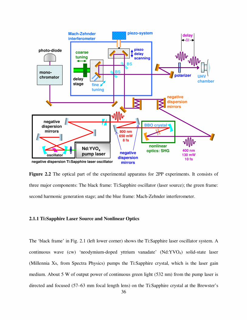
Figure 2.2 The optical part of the experimental apparatus for 2PP experiments. It consists of
three major components: The black frame: Ti:Sapphire oscillator (laser source); the green frame:
second harmonic generation stage; and the blue frame: Mach-Zehnder interferometer.
2.1.1 Ti:Sapphire Laser Source and Nonlinear Optics
The ‘black frame’ in Fig. 2.1 (left lower corner) shows the Ti:Sapphire laser oscillator system. A
continuous wave (cw) ‘neodymium-doped yttrium vanadate’ (Nd:YVO4) solid-state laser
(Millennia Xs, from Spectra Physics) pumps the Ti:Sapphire crystal, which is the laser gain
medium. About 5 W of output power of continuous green light (532 nm) from the pump laser is
directed and focused (57–63 mm focal length lens) on the Ti:Sapphire crystal at the Brewster’s
Nd:YVO4pump laser
∆t
negative dispersion Ti:Sapphire laser oscillator
800 nm650 mW
8 fs
nonlinear optics: SHG 400 nm
130 mW10 fs
BBO crystal
negative dispersion mirrors
delay stage fine
tuning
coarse tuning
BS
BS
piezo delay scanning
piezo-system
oscillator
negative dispersion
mirrors
polarizer UHV chamber
mono-chromator
photo-diode
Mach-Zehnder interferometer
delay
negative dispersion
mirrors

37
angle incidence 78 . The sapphire (Al2O3) crystal is doped with titanium ions (Ti3+, with
absorbance of 4.8 cm-1 and weight percentage of 045.0250.0 ± %). Ti:Sapphire lasers emit light
in the near infra-red region and are tunable within the range of 650–1100 nm; their gain is the
highest at 800 nm.
The bandwidth of laser output depends primarily on the properties of the gain medium, and
secondarily on the optical elements comprising the laser cavity. The Ti:Sapphire gain medium is
chosen for its broad bandwidth, high efficiency, and stability of operation. The laser cavity
consists of mirrors, which form a standing wave pattern of the electromagnetic field trapped
within the cavity. The constructive and destructive interference of the trapped field sets up
oscillation at discrete frequencies, termed the ‘longitudinal modes’ of the cavity. In the absence
of a frequency-selective optical element inside the cavity, the laser will oscillate in a multimode
fashion, on randomly selected modes within the spectral gain profile 79; while all other modes are
suppressed by depletion of the gain. If several modes can be made to oscillate with a fixed phase
instead of oscillating independently, the coupled modes interfere constructively in time to
produce periodical and intense bursts (or pulses) of light. This is known as the ‘mode-locked’
operation. Therefore, mode-locking is achieved by establishing a coupling between the phases of
the independently oscillating modes through a nonlinear process that favors phase-coherent
oscillation. A coherent superposition of the mode amplitudes is obtained, resulting in the
formation of laser pulses of extremely brief durations, as low as a few femtoseconds (10-15 s).

38
We employ the nonlinear ‘optical Kerr effect’ to mode-lock our laser. When an intense
monochromatic electromagnetic wave passes through a 3rd order nonlinear medium of a
centrosymmetric crystal, its dielectric response is expressed as
EE ⋅+= 2t εεε . [2.1]
The nonlinear dielectric response with this form requires the polarization of the form
EEEEP(3)
0(1)
0 χεχε +∝ [2.2]
where ε0 is the permittivity of free space, ( )1χ1ε += , and ( )32 χ1ε += , and χ(n) is the nth order
component of electric susceptibility 80. The nonlinear index of refraction of a medium is defined
as the square root of the ‘effective’ dielectric function (εeff):
( )
( ) 212
21eff
εε
εn
EE+=
=, [2.3]
where n2 is the 2nd order nonlinear refractive index. Since 02 nn << , it can be approximated by a
Taylor series expansion as 80
( )
( ) In21
nIn
||n2
1nn
20
20
+≈
+≈ EEE
, [2.4]
where the index of refraction varies linearly with the optical intensity (2
I E= ) on account of the
3rd order nonlinearity 81.
When an intense electric field is applied, it induces nonlinear polarization electrons with respect
to ionic cores. The nonlinear polarization of the medium leads to an intensity-dependent change
in the refractive index, as expressed in equation [2.4]. Because the laser beam intensity varies

39
transversely and peaks at the center of the beam profile, as illustrated in Fig. 2.3, the effective
value of the index of refraction follows its radial gradient. Under these conditions, the quadratic
index profile of the nonlinear medium acts as a focusing lens with an intensity-dependent focal
distance 79. In the case of our Ti:Sapphire laser, the laser crystal acts as the nonlinear Kerr
medium for phase-locking the modes within the laser cavity.
The transverse gain profile of a Ti:Sapphire laser is defined by the focal length of the lens
focusing 532 nm pump light into the Ti:Sapphire crystal. In the continuous mode of operation of
a Ti:Sapphire crystal laser, the cw mode is larger than the pump laser-defined gain medium. Self-
focusing of intense pulses oscillating within the cavity causes more optimal overlap of the mode-
locked operation cavity mode with the gain medium. Because high intensity fluctuations attain
better overlap with the gain medium, they are preferentially amplified to attain stable mode-
locked operation.
Figure 2.3 Kerr-lens mode-locking (KLM) in a 3rd order nonlinear gain medium acts as a lens
whose focusing power depends linearly on the intensity of the incident laser beam.
cw cavity modenonlinear gain medium
green pump laser beam
self-focusing of femtosecond beam
green pump laser beam
40
In addition to the self-focusing, the instantaneous intensity-dependent change in the index of
refraction induced a phase shift of the propagating field. The phase shift broadens the frequency
spectrum of the field, thereby increasing the bandwidth, which allows the laser to sustain shorter
pulses. The combined effects of this ‘self-phase modulation’ (SPM) and self-focusing lead to the
generation of more intense, broader frequency pulses up to the limits imposed by the gain
saturation, the bandwidth of the gain medium, and the bandwidth of the optical cavity elements.
In our Ti:Sapphire oscillator this passive Kerr mode-locking mechanism can sustain ~8 fs pulses
with 650 mW average output power and approximately 90 MHz repetition rate.
2.1.2 Second Harmonic Generation
Because the work functions of most metals lie within the range of 5.50.4 − eV, the photon
energy of 1.55 eV corresponding to the 800 nm wavelength is insufficient to induce 2PP. The
photon energy demands are even more severe for semiconductors, for which the gap from the
highest occupied state to Evac could be even larger. These considerations call for at least the
second harmonic of Ti:Sapphire laser to be employed in one-color 2PP studies of metal and
semiconductor surfaces.
Nonlinear optical conversion like second harmonic generation and sum frequency mixing can be
accomplished in nonlinear optical crystals. When two incident waves of angular frequencies ω1
and ω2 pass through a nonlinear medium, they can mix and thereby induce a nonlinear
polarization. The nonlinear polarization gives rise to new waves at frequencies 21 ωωω ±= ,
which traverse the nonlinear medium with a phase velocity ( )ωc/nω/kv ==ϕ . If the wave

41
vectors of the incident and induced waves conserve momentum the sum and/or difference
frequency waves can be produced with high efficiency. The ‘phase-matching’ condition
described above is expressed by 79
)(ω)(ω)ω(ω 2121 213 kkk ±=± [2.5]
for the three interacting photons.
Figure 2.4 The ‘phase-matching’ condition for a typical second harmonic generation process
where two incident waves (k1 and k2) and a resultant wave (k3) propagate collinearly.
As can be surmised from Fig 2.4, the maximum constructive interference between the
propagating sum-frequency wave and the locally generated wave can be obtained, when both of
the incident and resultant waves travel collinearly, i.e., 321 k||k||k , and with the same phase
velocity, i.e., |||||| 213 kkk += . Given that ω/kc/n = and 213 ωωω ±= , the phase-matching
condition can be rewritten in terms of indices of refraction and wave frequencies as
221133 ωnωnωn ±= [2.6]
where n1, n2, and n3 are the frequency and crystal axis-dependent indices of refraction.
k1
k2
k3nonlinear mediumχ(2)
k1(ω1) k2(ω2)
k3(ω1 + ω2)

42
In a second harmonic generation process, two photons of the same angular frequency ω mix to
produce a wave at 2ω. This process takes place within the ‘green frame’ shown in Fig 2.2. The
intensity of the second harmonic light in terms of that of the fundamental light is given by 79
( ) ( )( ) 2
2
033
22(2)eff
2
L∆kL∆ksin
ωIεcn
L|χ|2ω2ωI
⋅
⋅
= [2.7]
where I(ω) is the intensity of the fundamental wave, (2)effχ is the value of the effective nonlinear
susceptibility tensor element, ‘L’ is the length (or thickness) of the nonlinear doubling crystal.
The phase-mismatch parameter ‘∆k’ is defined as 12 2kk∆k −= , and is zero at the phase
matching condition. The effective second harmonic generation length is determined by the
‘coherence length’ of a doubling crystal, which is defined by the characteristic distance along
which the second harmonic waves remain in phase, and it is expressed as
)n4(n
λ
k2π
Lωo
2ωe
coh−
=∆
= . [2.8]
The efficiency of harmonic generation degrades when the fundamental and second harmonic
waves have a phase difference 2π∆ >ϕ , which happens if the thickness of the crystal exceeds
the coherence length, i.e., cohLL > . Then, the fundamental and second harmonic waves start to
interfere destructively, resulting in a decrease in the amplitude of the second harmonic wave.
Phase-matching can be achieved by employing a negative birefringent uniaxial crystal, for which
oe nn < , where ne and no stand for the extraordinary and ordinary indices of refraction,
respectively 82. The condition that gives the angle of propagation of incident light with respect to
the optic axis for which the extraordinary refractive index of the second harmonic light equals
that of the ordinary index of the fundamental light is defined by 80

43
( )( )( ) ( )( ) ( )( ) ( )( )( )2ωo
22ωo
2
22ωe
2
22ωe θn
1
n
θcos
n
θsin
θn
1=+= , [2.9]
whereby one can calculate the phase-matching angle ‘θp’ with respect to the optic axis in such a
crystal. The phase-matching condition can also be demonstrated graphically by the index of
refraction ellipses in Fig. 2.5. At θp, the indices of refraction of the fundamental and second
harmonic waves are equal, i.e., ( ) ( )ωo
2ωe nn = and the phase-matching condition is fulfilled. When
the incident light passes through the crystal at θp as an ordinary wave, the in-phase microscopic
contributions )(2ω ii rP , produce a macroscopic second harmonic wave of frequency 2ω as an
extraordinary wave.
Figure 2.5 The phase-matching condition for second harmonic generation process where a
negative birefringent uniaxial crystal is used. Type-I phase matching is employed where the
interacting incident fundamental waves have parallel polarization and the resultant wave is
orthogonal to the input waves. The phase-matching angle θp corresponds to the intersection of
the ordinary and the extraordinary index curves. The eccentricities shown are exaggerated.
no(2ω)(θθθθ)
no(ω)(θθθθ)
koptic axis (z)
ne(2ω)(θθθθ)
ne(ω)(θθθθ)
θθθθp

44
The optical arrangement of the second harmonic generation system is shown in Fig. 2.6. For
frequency doubling or sum-frequency generation, various nonlinear media can be employed. We
choose the BBO (β-BaB2O4) crystal, which has a large nonlinear coefficient, low temperature
dependence, high damage threshold, high optical homogeneity, large angular acceptance, and a
transparency range between 3500195− nm 79. A pair of spherical concave mirrors with 50 mm
focal length is employed to focus the fundamental wave on the BBO crystal and to collimate the
generated second harmonic light. The mirrors are mounted on translation stages to optimize
focusing of 800 nm light onto the BBO crystal, and the generated second harmonic beam onto
the sample in the photoemission chamber. The BBO crystal has 80 µm thickness; it produces a
second harmonic wave with about 20% efficiency. The second harmonic light has ~200 meV
spectral bandwidth centered at 400 nm and 10 fs pulse duration. The BBO crystal is mounted on
a gimbal mount, which enables us to optimize the phase-matching condition. By changing the
phase-matching angle θp, according to equation [2.9], we can tune the center output photon
energy between 3.00 to 3.20 eV. This is possible, because the crystal cannot phase-match the full
bandwidth of the fundamental pulse; changing the angle selects different frequencies for which
the phase-matching condition is fulfilled.

45
Figure 2.6 The optical arrangement inside the second harmonic generation stage: the
fundamental wave is focused onto the BBO crystal at the phase-matching angle θp, giving rise to
the second harmonic wave through type-I frequency doubling.
In Fig. 2.7, we juxtapose the spectra of the fundamental wave taken at the exit of the laser cavity
and the second harmonic wave taken right after the second harmonic generation stage. The
fundamental wave has a broad asymmetric spectrum, and the second harmonic wave exhibits a
Gaussian shape spectrum centered at 400 nm.
θθθθp
fundamental wave
second harmonic wave
ω1ω2ω3
BBO
phase-matching angle
mirror
mirror
inte
nsity
[arb
. u.]
900850800750700650wavelength [nm]
inte
nsity
[arb
. u.]
440420400380360wavelength [nm]
Fundamental SHG
inte
nsity
[arb
. u.]
inte
nsity
[arb
. u.]
wavelength [nm] wavelength [nm]

46
Figure 2.7 The fundamental (left) and second harmonic (right) spectra of the Ti:Sapphire laser.
According to Heisenberg’s uncertainty principle for a Gaussian shape pulse, the time–bandwidth
product is expressed as 80,83
π
2ln2∆τ∆ν =⋅ . [2.10]
where the bandwidth can be calculated by differentiating frequency with respect to the
wavelength in λcν = as 79
2λ
∆λc∆ν
⋅= . [2.11]
The second harmonic laser pulse is centered at 400 nm and has a full-width half-maximum
(FWHM) of about 23 nm. Therefore, the minimum pulse width can be estimated as
( )fs10
)m1023)(m/s103(
)m10400(π
2ln2∆λcλ
π
2ln2∆ν
π2ln2∆τ
98
292
≈
××
×
=
⋅
==
−
−
. [2.12]
The pulse duration can be confirmed by autocorrelation measurements at the sample surface.
2.1.3 Interferometric Pump and Probe Delay Scanning
We employ a ‘Mach-Zehnder Interferometer’, abbreviated as MZI (the ‘blue frame’ in Fig. 2.2),
in order to create identical pump and probe pulses with a well-defined time delay 71,78. In the
MZI, the input beam is separated into two beams by a partially transmissive beamsplitter. After
traversing two different optical paths, the two separated beams are recombined on a second
beamsplitter. The difference between the optical paths gives the temporal or the phase delay
between the two pulses. An MZI has two output beams, which differ by an additional π phase

47
shift corresponding to the difference in the number of reflections each beam suffers on passing
through the interferometer. By translating one pair of retroreflecting mirrors back and forth with
a piezo-driven flexure stage, the length of one of the arms is continuously scanned to produce a
variable time delay between the pulse pair.
The MZI has two output beams, which serve different purposes. The output beam for which the
dispersion is balanced is used for 2PP experiments, while the unbalanced one is used to monitor
and control the scan delay. After exiting the MZI and right before entering the UHV chamber,
the excitation laser beam passes through a λ/2-wave plate, by which one can select s- or p-
polarized light. The beam goes through the viewport of the chamber, which is made of a plano-
convex CaF2 lens with a nominal focal distance of 200 mm. The lens focuses the beam on the
sample as well as maintains the vacuum within the chamber. The diameter of the laser spot
formed on the sample is approximately 70 µm 84.
2.1.4 Measurement of the Laser Pulse Duration
We employ ultrafast lasers to probe the electronic structure and electron dynamics at metal
surfaces. Because many dynamical processes at surfaces occur on the time scale of the
femtoseconds, it is essential to be able to characterize and accordingly optimize such pulses. The
femtosecond regime is beyond the detection range of standard electronic instruments; therefore,
we employ a pure optical method based on optical second-order autocorrelation technique to
characterize directly not only the amplitude but also the phase of the laser pulse 80. In MZI, the
optical pulse from the laser is split into two identical pulses (‘pump’ and ‘probe’), which travel

48
different paths of nearly equal lengths before they are made collinear at the output of MZI 79. The
time delay between the two pulses is scanned and a second-order interferometric autocorrelation
trace of a Ta sample plate is measured by TR2PP to check the quality of the laser pulse (see
section 2.1.5 for further information). Optimization of the pulse is achieved by minimizing the
overall dispersion in the optical path length through successive reflections of the laser light from
negative dispersion mirrors; the dispersion compensation will be discussed in the following
section 78.
The first-order interferometric autocorrelation in terms of pump and probe electric fields (i.e.,
electric field autocorrelation) and their delay τ is expressed as
( ) ( ) ( ) ( ) ( ) ( ) ( )τGτGtτtdttτtτI *2221 +++−=+−= ∫
+∞
∞−
EEEE [2.13]
where G(τ) is the first order autocorrelation of a signal function with respect to a reference
function, and G*(τ) is its complex conjugate:
( ) ( ) ( )∫+∞
∞−
= dtτ-tFtFτG refsig . [2.14]
Here, both the signal and the reference functions are identical electric fields, except for the time
delay τ. Therefore, G(τ) can be expressed as ( ) ( )tiω(t)expτ)(t~τG lEE − , indicating that it and
its conjugate G*(τ) oscillate with an average frequency ωl. The Fourier transform of G(τ) is
( ) ( ) ( )
( ) ( )( )ωI
ωEωE
dτiωexpτGωG
*
∝
⋅∝
−⋅= ∫+∞
∞−
τ
. [2.15]

49
In other words, the Fourier transform of the first-order autocorrelation G(ω) is proportional to the
spectral intensity of the laser pulse. Thus, the first-order field autocorrelation does not reveal
information other than what can be gained from a spectrum acquired with a spectrometer 83.
In order to gain more information on the shape and phase of the laser pulse, the nonlinear
second-order interferometric autocorrelation technique should be used. It can be achieved by
coherently superposing the two collinear partial beams, and scanning their delay with the
interferometric (subwavelength) precision. It is expressed as
( ) ( ) ( )[ ]∫+∞
∞−
+−= dttτtτI22
2 EE . [2.16]
If the pump and probe electric fields are described by ( )[ ](t)ωtiE(t)exp ϕ+ and
( )[ ]τ)-(tτ)-ω(tiτ)exp-E(t ϕ+ respectively, where E(t) is the slowly varying amplitude, their
second-order interferometric autocorrelation is given by
( ) ( )[ ] ( )[ ][ ]{ }∫+∞
∞−
+++= dt(t)tωiE(t)expτ)-(tτ)-(tωiτ)exp-E(tτI22
ll2 ϕϕ . [2.17]
After expanding equation [2.17], one obtains the following:
( )
( ) [ ]
( )[ ]dt)τt()t(τω2cos)τt(E)t(2E
)τt()t(τωcos)τt(E)t(E)τt(E)t(4E
)τt(E)t(4E)τt(E)t(EτI
l22
l22
22442
−−+−+
−−+−+−+
−+−+= ∫+∞
∞−
ϕϕ
ϕϕ . [2.18]
The above expression is divided into three components: the first, second and third lines of the
integral represent the phase averaged signal, and envelopes at ω and 2ω frequencies, respectively.
Note that the phase averaged signal is independent of the phase, whereas the first and second

50
order envelopes oscillate at 1ωl and 2ωl frequencies respectively and contain explicit phase
information, which can be used for diagnostic purposes for the determination of the laser pulse
dispersion.
One can use equation [2.18] to calculate the relative intensities of second-order interferometric
autocorrelations, when the pump-probe delay is zero (i.e., 0τ = ) as
( ) ∫== dt)t(E20τI 442 , [2.19]
and when the time delay is far from coherent superposition at very large delay (i.e., ±∞→τ ) as
( ) ∫=±∞→ dt)t(E2τI 42 . [2.20]
Therefore, the corresponding contrast ratio is 8:1. We present the results of a simulation based on
equation [2.18] for several chirp parameters and display a TR2PP measurement on a Ta sample
plate in section 2.1.5. Their respective contrast ratios turn out to be 8:1 as computed here.
2.1.5 Characterization of the Laser Pulse and the Effects of Dispersion
In optics, dispersion is defined as the frequency (or wavelength) dependence of the phase
velocity of a wave. When an ultrashort optical pulse propagates through a transparent medium,
which may include optical elements (lens, beamsplitter, etc.) and even air, it suffers a phase
distortion on account of its wide spectral width and the group velocity dispersion (GVD) of the
medium through which it propagates. This phenomenon leads to change in pulse duration along
the propagation path 80. Each medium contributes to the total GVD, resulting in the pulse
broadening. In femtosecond regime, this effect has substantial consequences and needs to be
compensated. To do so, we reflect the laser pulse from pairs of mirrors that have dielectric stacks
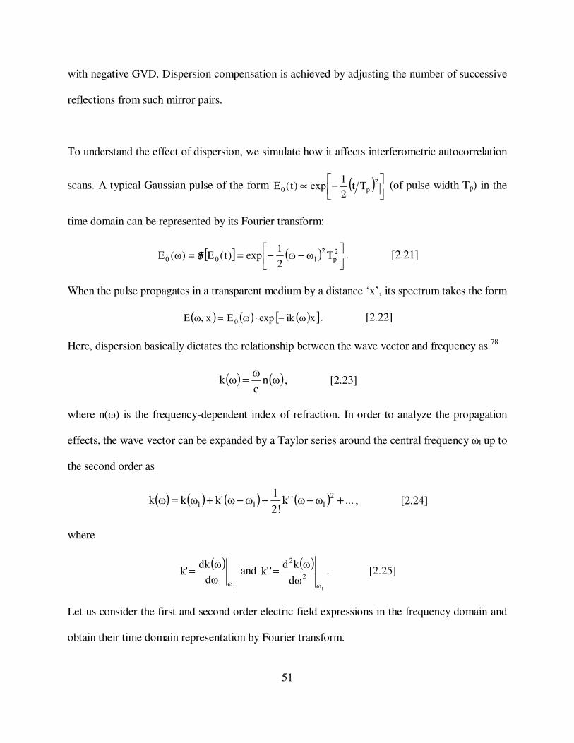
51
with negative GVD. Dispersion compensation is achieved by adjusting the number of successive
reflections from such mirror pairs.
To understand the effect of dispersion, we simulate how it affects interferometric autocorrelation
scans. A typical Gaussian pulse of the form ( )
−∝
2p0 Tt
21
exp)t(E (of pulse width Tp) in the
time domain can be represented by its Fourier transform:
[ ] ( )
−−== 2
p2
l00 Tωω21
exp)t(E)ω(E FFFF . [2.21]
When the pulse propagates in a transparent medium by a distance ‘x’, its spectrum takes the form
( ) ( ) ( )[ ]xωikexpωExω,E 0 −⋅= . [2.22]
Here, dispersion basically dictates the relationship between the wave vector and frequency as 78
( ) ( )ωncω
ωk = , [2.23]
where n(ω) is the frequency-dependent index of refraction. In order to analyze the propagation
effects, the wave vector can be expanded by a Taylor series around the central frequency ωl up to
the second order as
( ) ( ) ( ) ( ) ...ωω'k'2!1
ωωk'ωkωk 2lll +−+−+= , [2.24]
where
( )
lωdωωdk
k'= and ( )
lω
2
2
dω
ωkd'k' = . [2.25]
Let us consider the first and second order electric field expressions in the frequency domain and
obtain their time domain representation by Fourier transform.

52
The first term, after a propagation distance L, can be written as
( ) ( ) ( )
−+
−−=
−= Lωω'k
cnω
kiexp)ω(ELωkc
nωiexp)ω(E)ω(E lll00
1 . [2.26]
Its Fourier transform gives us the electric field in the time domain as
( )( ) ( )( )
( )τtδLcωn
ω
ktiωexptEtE
l
l00
1 −⋅
−−⋅= , [2.27]
where the time delay is expressed as
( ) ( ) ( )
⋅=
−=
ll ωω dωωdn
ωcL
Lcωn
dωωdk
τ . [2.28]
Note that the first order dispersion term turns out to be simply a time delay and does not contain
any phase information; therefore, it can be neglected.
The second term of the electric field in the frequency domain can be written as
( )( ) ( ) ( )
( )
( )
+−−≈
+−−=
−−⋅=
2
2p
''l2
p2
l
2p
''l2
p2
l
2l
''l0
2
L2T
ki1Tωω
21
exp
LT
ki1Tωω
21
exp
Lωωk21
iexpωEωE
. [2.29]
The second order dispersion term turns out to be the GVD, and for a small value, the Fourier
transform of the above expression becomes
( )( ) ( )
+
−=
−
−= iξ1
Tt
21
expLT
ki1
Tt
21
exptE
2
p2p
''l
2
p
2 . [2.30]
It turns out that the GVD corresponds to the linear chirp defined for a Gaussian pulse as

53
( ) ( )
+⋅−=−=
llωω
2
2
l2p
l2p dω
ωdn2
dω
ωndω
cT
L''k
T
Lξ , [2.31]
where ‘ξ’ is the chirp parameter. If one combines the first and second order dispersion terms by
convolution, the following quantitative expression is obtained:
( ) ( )( ) ( )( ) ( )
+
−−=⊗= iξ1
Tτt
21
exptEtEtE
2
p
22 . [2.32]
If a linearly chirped Gaussians laser pulse ( ) ( )
+
−−= iξ1
Tτt
21
exptE
2
p
is substituted in the
integrals in equation [2.18], the resulting interferometric second-order autocorrelation becomes
( ) ( )[ ]
( ) ( ) ( )
( )( )[ ] ( )τ2ωcosTτξ1exp
τωcosTτ2a
cosTτ4ξ3
4exp
Tτ2exp1τI
l2
p2
l2
p2
p
2
2p2
+−+
+−+
−+=
. [2.33]
As stated in section 2.1.4, the fundamental, first order and second order envelopes modulate the
0ω, 1ω and 2ω frequencies, respectively. In order to visualize the effect of chirp on the second-
order interferometric autocorrelation signal, one needs to calculate and plot the corresponding
signal as a function of the delay time for various values of ξ. In Fig. 2.8, we plot the second-
order interferometric autocorrelation for different values of ξ for a pulse centered at 400 nm with
the corresponding optical cycle of 1.33ω2πT l == fs, and the pulse duration 10Tp = fs. In our
experiments, the chirp parameters ξ lies in the range of 30 − .

54
Figure 2.8 Second order interferometric autocorrelation (I2PC) for various chirp parameters ξ.
The contrast ratio between the signal at 0τ = and ±∞→τ is 8:1, as expected from the
calculation.
The second-order interferometric autocorrelation of a laser pulse can be performed by means of
the TR2PP technique. An interferometric two-pulse correlation (I2PC) measurement obtained by
scanning the pump-probe delay interferometrically and recording the 2PP signal at a specific
photoemission energy can converge to an interferometric autocorrelation measurement under the

55
assumption that the material responds instantaneously to the applied field. We perform such an
I2PC measurement by exciting 2PP signal from a Ta sample plate within our UHV chamber.
Because Ta has a high density of d-band states at EF, its intermediate state lifetime is extremely
short, and therefore, we assume that it causes minimal distortion of the autocorrelation scan. Fig.
2.9 compares a simulated interferometric autocorrelation by equation [2.18] for 0ξ = (top) and a
typical I2PC scan acquired by measuring TR2PP from the Ta sample plate (bottom). From the
close correspondence between the simulation and I2PC measurement, one can conclude that the
nonlinear interferometric autocorrelation signal from Ta plate is an effective tool for measuring
the pulse characteristics and compensating the dispersion in order to minimize the laser pulse
duration at the sample. As expected from equation [2.18], the experimental measurement
approaches the theoretical ratio of 8:1.
Figure 2.9 Interferometric autocorrelation signal obtained by simulating equation [2.18] with
0ξ = (top) for a 10 fs Gaussian pulse, and an experimental I2PC scan obtained by recording
2PP signal from a Ta sample plate (bottom).
1.0
0.8
0.6
0.4
0.2
0.0-40 -20 0 20 40
Time delay [fs]-50 -40 -30 -20 -10 0 10 20 30 40 50
8
6
4
2
0
pump–probe delay time [fs]
-50 -40 -30 -20 -10 0 10 20 30 40 50pump–probe delay time [fs]
8
6
4
2
0
simulation
experiment
I2P
C s
ign
al i
nte
nsi
ty [
arb
. u.]

56
2.2 Ultrahigh Vacuum Chamber and Related Instruments
Atomic level characterization of solid surfaces requires that the composition of the surface stay
constant during the experiment 18. This implies that the flux of atoms or molecules impinging on
the surface from the ambient environment must be minimized. This can be achieved if the
experiment is performed under UHV conditions, which require pressures below ~5×10⁻¹⁰ mbar
15,18.
2.2.1 General Features of the Ultrahigh Vacuum Instrument
2PP measurements are performed in a UHV chamber (built by Omicron Vakuumphysik GmbH).
The pressure within the chamber is maintained in the range of 1.0×10⁻¹⁰ to 2.0×10⁻¹¹ mbar; as a
result the surface can remain clean for several hours, which is typically 6-9 hours in our
experiments. At this pressure level, the molecular density is 6102 × per cm3, and the molecular
arrival rate is about 10103 × molecules cm-2s-1, corresponding to a monolayer arrival time of the
order of 10 hours 18. In practice, many impurities, such as H2, would not stick to and contaminate
the surface.
Although the UHV chamber can be pumped down, there is always some amount of adsorbed
gases on its interior walls, and their ensuing desorption limits the ultimate pressure. Therefore,
the chamber needs to be baked over a period of 12–36 hours at some 140–150 °C temperature,
after it has been exposed to air. The chamber is manufactured from µ-metal to screen external

57
magnetic fields, which would perturb low energy electrons. Exceeding this temperature limit
may lead to trapping of magnetic fields, which would effectively make the chamber useless for
electron spectroscopy. The duration and temperature of the bakeout process depend on the
degree of contamination.
Pumping the chamber from 1 Atm to some 2×10-11 mbar level requires several pumping stages.
In general, pumps can be divided into two main categories, (1) roughening pumps to evacuate
the chamber down to 64 1010 −−− mbar, and (2) the pumps for the UHV-regime 85. In our UHV
system, we employ a rotary vane pump, a turbo-molecular pump, an ion pump and an auxiliary
titanium sublimation pump.
Rotary vane pumps are used in conjunction with turbo-molecular pumps and their function is to
bring the pressure down to the 10-3 mbar level. According to Fig. 2.10(a), gas enters through the
inlet and gets trapped in the volume between the rotor vanes and the stator; as the eccentrically
mounted rotor turns, the gas is compressed and forced through the exhaust valve. Turbo-
molecular pumps operate in the 10-4–10-6 mbar pressure range. As shown in Fig. 2.10(b), a
turbine rotor, which is composed of a stack of rotor blades with tilted leading edges, spins at very
high speed (about 50,000–100,000 rpm) and shuffles gas molecules from the UHV side to the
backing side, where they are pumped away by a rotary vane pump. Ion pumps are reliable,
durable, and vibration-free; they operate in 113 1010 −− − mbar range and are especially effective
in maintaining the UHV conditions. As shown in Fig. 2.10(c), an ion pump consists of a
collection of short, stainless steel anode tubes (a multicell array) situated between two titanium
cathode plates, leaving a gap on both sides. A high potential (3000–7000 V) is applied between

58
anode and cathode, in the presence of a strong magnetic field. Electrons discharged from the
cathode plates follow a helical trajectory to the anode plates. Because of their high energy,
electrons ionize gas molecules. The ionized molecules are subsequently accelerated by the
electric field and strike the cathode plates, which leads to sputtering of Ti atoms from the
cathode. The sputtered Ti coats the interior walls of the cells, the cathode plates and the pump
walls, where it chemically traps gas molecules that impinge 18,86. Titanium sublimation pumps
(TSP), as displayed in Fig. 2.10(d), are also used at low pressures in addition to ion pumps.
Titanium is intermittently sublimated by passing a current through the Ti filaments. Reactive gas
molecules such as nitrogen, oxygen, hydrogen, CO, CO2 and water react with the exposed Ti
film to form nonvolatile compounds; hence, low pressure is attained.
oil
rotor
vane
stator
inletexhaustrotor
stator
motor
rotor blades
stator blades
(a) (b)
discharge valve
S Ntitanium cathode plates
magnets
V
anode tubes
titanium sublimation filaments
stainless steel ground rod
(c) (d)

59
Figure 2.10 Schematic descriptions of (a) a rotary vane pump, (b) a turbo-molecular pump, (c)
an ion pump (with its multicell structure), and (d) a titanium sublimation pump (TSP).
Having an apparatus to monitor the pressure of the UHV chamber is as important as having
vacuum pumps to reach and maintain low pressure, especially during an experiment. There is no
universal vacuum gauge for this purpose; different gauges function at different pressures for
different experiments. Pressure under UHV conditions is usually measured by an ion gauge,
which operates in the 114 1010 −−− mbar pressure range. As its name suggests, its operation is
based on the ionization of the gas molecules. The ion current depends on the gas pressure,
whereby the pressure can be determined.
One also needs to know about the gas composition in an UHV chamber, especially when an
experiment is being conducted. This can be accomplished with a Residual Gas Analyzer (RGA),
of which the most widely used type is the Quadrupole Mass Spectrometer (QMS). Mass
spectroscopy of the gas in the chamber is needed (1) to monitor the exposure of surfaces to
specific gases, (2) to monitor desorption from surfaces, and (3) to detect any malfunction of the
UHV system. In general, a properly baked UHV system has residual background gases
containing a mixture of H2, CO, CO2, and N2.
Our UHV chamber, its components and auxiliary instruments are illustrated in Fig. 2.11. The
UHV analysis chamber is where the actual experiments are conducted. The top view (Fig.
2.11(a)) shows the direction of the incident laser beam and that of photoemitted electrons that are
captured by a hemispherical energy analyzer. The side view (Fig. 2.11(b)) shows how other

60
UHV components and related devices are located and connected to each other. There is a smaller
‘load lock chamber’ attached to the analysis chamber that is used to load, remove, exchange, and
store samples in a revolving sample holder under UHV conditions.

61
magnetic transfer probe
UHV analysis chamber
wobble stick
templiquid
N2 tank
RGA
Ar+
cyl.
Ar+ gun
Ar+
ion pump rotary pump
TSP
laser
load-lock chamber
hemispherical energy analyzer
ion gauge
gate valve
manipulator
pirani gauge
sample
X Y
Zφφφφ
turbomolecular pump
outlet
valve
valvevalve
valve
valve magnet
byp
ass
(b)
alkali dispenser
UHV analysis chamber
magnetic transfer probe
laser
load-lock chamber
valve
magnet
e-
reflection
hemispherical energy analyzer
manipulator
(a)
sample

62
Figure 2.11 The (a) top view and (b) side view of our UHV system (TSP: titanium sublimation
pump; RGA: residual gas analyzer; temp: temperature controller). The alkali metal dispensing
unit is shown in more detail in Fig. 2.12.
There are several valves in the UHV system, each of which serves a different purpose. The
function of the large gate valve is to cut off the analysis chamber from the turbo-molecular pump.
It is actuated by high-pressure gas, and will close in the case of a power failure to protect the
chamber from contamination with atmospheric gases. A manual valve is used between the
analysis chamber and the load lock chamber, and another one between the latter and the turbo-
molecular pump.
Our UHV system is also equipped with a 4-axis sample manipulator. It is used to move the
sample in the x-, y- and z-directions, and to rotate it around the z-axis for angle-resolved
measurements. The manipulator is designed such that the center of rotation can be made
coincident with the incident laser beam where it hits the surface of the sample. Its center is a
hollow cylinder, in which liquid nitrogen is introduced to cool down the sample. It is also
possible to heat the sample by electron bombardment. By applying a high potential difference
(about 1 kV) with respect to the sample, electrons emitted from a hot tungsten filament (carrying
about 2 A current) are accelerated and hit the back of the sample plate. The energy provided by
the electron current is the main mode of heating the sample. Temperature can be varied by
adjusting the applied voltage and the electron emission current. Through cooling by liquid
nitrogen and heating by electron bombardment we are able to control the sample temperature
between 85–800 K. The upper part of the manipulator is a hollow tube made of stainless steel,

63
whereas the lower part is made of ‘silver’ (in a later version ‘copper’) and is braised to the
stainless tube. The bottom of the manipulator is made of solid silver (copper) and is attached to
the upper silver (copper) component. A thin sapphire plate is sandwiched between the two silver
(copper) parts to provide high thermal conductivity and electric insulation. The bottom silver
(copper) part holds a sample holder that accepts a Ta sample plate to which is attached a noble
metal sample. The sample plate is fastened to the holder by flexible ‘Mo’ springs. Temperature is
measured by means of an N-type (nicrosil-nisil) thermocouple, which is spot-welded onto one of
the springs. All components in the vicinity of the sample, including the thermocouple and the
screws, are made of nonmagnetic materials. Also, all insulating materials near the sample are
shielded by metal foil. Both precautions are taken to prevent perturbation of low energy electrons
by stray magnetic and electric fields.
According to Fig. 2.11, the hemispherical energy analyzer is at the ground potential as the rest of
the UHV chamber 78. The inner surface of the energy analyzer is coated with a layer of graphite
to provide a homogeneous work function of 4.50 eV. The sample mounted on the manipulator is
electrically insulated from the analysis chamber by a sapphire plate, which acts simultaneously
as an electrical insulator and an effective thermal conductor. This allows us to apply a bias
voltage of several volts between the sample and the analyzer, in order to improve the detection
efficiency of low energy photoelectrons. The application of a bias voltage is necessary to
minimize the residual influence of stray electric and magnetic fields within the chamber. The
undesirable effect of the applied bias is to modify the angular distribution of photoemission,
which has to be accounted for in angle-dependent measurements.

64
A home-made alkali metal dispensing unit (Fig. 2.12) is employed in the experiments involving
alkali atom adsorption. This unit can accommodate three compact getter sources (SAES getters),
each of which contains a mixture of an alkali metal chromate and a reducing agent. The reducing
agent is a getter alloy called ‘St101’ (84% Zr and 16% Al). In addition to reducing the alkali ions
back to their metallic state, St101 also removes chemically reactive gases from the environment,
preventing them from contaminating the alkali metal vapor 87. An electric current is applied
through the getter source to emit alkali atoms through a slit. After applying a threshold current
specific to each alkali atom species, the onset of adsorption of alkali atoms on the sample
(Cu(111) or Ag(111)) can be seen through changes in the 2PP spectrum of the substrate. The
deposition rate on the sample surface can be controlled by adjusting the current. This enables us
to control the deposition rate and attain reproducible alkali atom coverage. The precise direction
of the beam of alkali atoms must be aligned with respect to the position of the sample before
taking actual data. To do so, the tilted flanges shown in Fig. 2.12 are rotated against each other,
which enables directing the one of three separate getter sources toward the sample. Although the
dispenser ejects alkali atoms effusively, only a narrow beam of alkali atoms passes through the
rectangular exit aperture, which functions as a collimator. It is essential to direct the beam of the
alkali atoms precisely onto the sample to achieve uniform alkali atom coverage throughout the
sample surface. The coverage uniformity ensures uniform work function reduction; this
minimizes lateral field gradients at the sample surface, which can interfere with detection of low
energy electrons.

65
Figure 2.12 Alkali metal dispensing unit containing three alkali metal dispensers. The tilted
flanges are moved against each other to align the exact direction of the beam of alkali atoms,
while the shutter is used to start or halt alkali atom deposition.
2.2.2 Energy Analyzer
A typical experimental setup for photoemission spectroscopy consists of a combination of an
electron lens system and an energy analyzer. Most analyzers use electrostatic forces for electron
separation according to their kinetic energies and fall into two categories: (1) retarding field and
(2) deflection analyzers.
We employ a deflection-type electrostatic electron energy analyzer of hemispherical shape
(Omicron, EA-125), which is called a ‘Spherical Deflection Analyzer’ (SDA) 3 or a ‘Concentric
Hemispherical Analyzer’ (CHA) 18. Photoemitted electrons are analyzed with respect to their
kinetic energy and momentum. A set of imaging and energy-dispersive electron optical elements
are used as in a conventional spectrometer for photons. The notion of refraction (deflection)
power supply
to sample
alkali metal dispersers
turnableshutter
tilted flangesknobs
exit aperture
dispenser slit
beam of alkali atoms

66
defined by Snell’s law in conventional optics can also be used to define the trajectories of
photoelectrons by replacing refraction indices by the perpendicular components of electron
velocity:
==
⊥
⊥
inc
ref
inc
ref
ref
inc
nn
v
vsinθsinθ
. [2.35]
The beam of photoelectrons is refracted toward or away from the normal to the equipotential
lines depending on the potential gradient as illustrated for metallic apertures in Fig. 2.13 15.
Figure 2.13 Electron lens formation by means of metallic apertures and the subsequent
deflection of photoelectron trajectories in a (a) focusing and (b) defocusing setup.
When photoelectrons enter the energy analyzer, they pass through a multi-element electrostatic
lens with 30 mm working distance. The lens system consists of two consecutive lenses, which
collect electrons from the sample and focus them on the entrance aperture of the hemispherical
energy analyzer 88 . The first ‘Einzel’ lens selects the analysis spot size and the electron
acceptance angle; it has three magnification modes: high, medium and low. In the high (low)
magnification mode, the focal plane is close to (far from) the sample and the lens accepts a wide
(narrow) angle of incoming photoelectrons from a small (large) area. We use the ‘low’ mode,
0 0 + electron trajectories
(a) focusing (b) defocusing
0 + +

67
since its angular resolution of ±1° offers the highest momentum resolution. The second ‘focusing’
lens accelerates or decelerates photoelectrons to adjust their kinetic energy to match the ‘pass
energy’ (Ep) of the analyzer. The pass energy is the kinetic energy that photoelectrons must
possess to have the appropriate trajectory from the entrance to the detector within the
hemispherical energy analyzer. The second lens ensures that the focal point remains on the
analyzer’s entrance aperture.
The role of the analyzer is to resolve photoelectrons with respect to their energy 18. The pass
energy of transmitted electrons is controlled by the potential difference V0 across the electrodes
of the analyzer. Our energy analyzer has a mean radius (R0) of 125 mm, and its structure and
components are schematically presented in Fig. 2.14.
1st lens
2nd lens
outer hemisphere
inner hemisphere
UHV vessel
RoutR0
Rin
samplephotoelectrons
channeltrons
detector
V0
exit apertures
entrance aperture

68
Figure 2.14 Schematic details of the hemispherical electron energy analyzer. Photoelectrons
entering the instrument pass through two electron lenses and the entrance aperture. When they
are in the hemispherical zone, they follow a circular path and arrive at the 7-channel channeltron
array where they are detected. Each channel measures a slightly different trajectory from the
others corresponding to a specific kinetic energy.
There is a set of variable slits at the entrance of the hemispherical analyzer, which adjust the
transmission characteristics such as the number of photoelectrons and the energy resolution. The
potential difference V0 between the inner and the outer hemispheres of the analyzer is
responsible for defining the radius of the circular photoelectron trajectories between the two
hemispheres. Photoelectrons traveling between the hemispheres with an average energy ‘eV0’
follow slightly different trajectories between the entrance and the exit apertures according to
their kinetic energy dispersion. The 7-channel channeltron detector collects these arriving
photoelectrons according to their energy. The size of the exit slit is also variable. Wide (narrow)
slits provide coarse (fine) energy resolution with correspondingly high (low) photoemission
signal intensity. The photoemission current within the energy window of a specific size slit is
recorded as a function of energy with respect to EF. The scanning of photoelectron energies to
obtain photoemission spectra is accomplished by holding the pass energy fixed and varying the
retarding voltage within the lens system to match the incoming electron kinetic energy to the
pass energy. The matching occurs through a potential difference between the adjacent cylindrical
electrodes within the lens system. Usually, we combine the spectra from the seven channels to
obtain a combined photoemission spectrum, which describes the overall energy distribution of
the photoelectrons.

69
The energy resolution of the analyzer can be estimated from 88
+= 2
0p α
2Rd
E∆E , [2.36]
where ‘Ep’ is typically 5 eV, ‘d’ is the width of the entrance slit (we usually use a circular
aperture with 2 mm diameter), and ‘α’ is the half-acceptance angle for the incoming
photoelectrons in radians (we generally use the ‘Low Magnification’ mode with π/1801α o=≈ )
78. Under these conditions, an energy resolution of less than or equal to 20 meV is attainable 89.
This is considerably smaller than the transform limited width of a ~10 fs duration excitation laser
pulse. As equation [2.36] implies, our analyzer is operated in the ‘Constant Analyzer Energy’
(CAE) mode, which uses a fixed pass energy.
2.2.3 Detection of Photoelectrons
To obtain the highest sensitivity, it is necessary to count single electrons. Therefore, we use an
array of seven channeltron detectors, with dedicated counting electronics for each channel.
According to the sketch in Fig. 2.15, channeltron detectors multiply the electron current triggered
by single electrons hitting their entrance (cathode) surface. The channeltrons consist of hollow,
ceramic tubes that are curved. Because a bias of 2–3 kV is applied across the channeltron, the
electrons are accelerated toward the anode. As electrons travel down the tube, they scatter many
times along their trajectories to the anode. Each time they impinge on the ceramic surface, they
generate multiple secondary electrons. Through this multiplication process one electron is able to
produce a pulse of 87 1010 − electrons, which are collected at the anode.

70
Figure 2.15 Amplification of a single photoelectron arriving at the entrance of a channeltron.
2.3 Acquiring and Recording the Photoemission Data
2.3.1 Energy-Resolved Photoemission Experiments
The photoelectron counts collected at the channeltron ‘output’ (Fig. 2.15) are sent to the data
acquisition electronics depicted in Fig. 2.16. The electronics transform the analog electronic
signals from the channeltrons into digital optical pulses, which serve as digital inputs to a digital
acquisition card. The first component in the device (‘input protection’) employs a capacitor to
isolate the high voltage (about 2-3 kV) applied across the channeltron and transmits to a
‘wideband pulse amplifier’ to be amplified. The signal exiting the amplifier has pulses of
3.13.0 − V amplitude and approximately 25 ns duration; and sent to a ‘discriminator’, a
threshold control device, which is set to accept signals at or above a certain voltage (50 mV in
our case) 90,91. This voltage is set to reject low-intensity pulses generated as noise that do not
primary electron
secondary electrons
output
HVanode

71
carry information on photoelectron counts. Next, the pulse signal is converted to a digital signal
and sent to a ‘high-speed comparator’, which detects the pulses above the preset threshold. Then,
the pulse passes through the ‘dead time control unit’, where its width is set to 35 ns and the dead
time between pulses to 70 ns. This is regulated by external parameters. Afterwards, the pulses
coming from the dead time control unit are transmitted to the ‘pulse counter’ where a digital
acquisition card receives the signal via fiber-optic cables and counts the number of digital pulse
events in a data acquisition cycle. When the next signal arrives, the computer clears the memory
and starts a new cycle. This procedure continues during data acquisition and the computer
compiles the data.
Figure 2.16 Electronics employed to acquire the photoemission counts.
The 7-channel channeltron introduced in the preceding section receives photoelectrons at slightly
different kinetic energies (with intervals of 0.1 eV in our default mode). The signals coming
from each channel are collected, counted and processed separately. One has the freedom to
pulse counter
input protection
C
wideband pulse amplifier
dead time control
unit
external settings
high-speed comparator
signal through fiber-optics
data acquisition device
channeltronoutput
~25 ns
discriminator
~50 mV
~35 ns

72
display photoemission spectra of all seven channels separately or as a sum of component spectra.
Photoemission spectra belonging to a Ag(111) surface are presented just the way they are
recorded, when seven channels are separated (top) and combined (bottom) in Fig. 2.17.
Figure 2.17 Photoemission spectra of a Ag(111) surface, when seven channeltron channels are
recorded separately (top) and combined into a single spectrum (bottom). The energy axis is
incremented by 2 V because of the applied bias voltage.
2.3.2 Time-Resolved Photoemission Experiments
In addition to energy-resolved 2PP experiments, we also carry out TR2PP measurements, where
we measure the photoemission current at well-defined energies as a function of the time delay
between identical pump and probe laser pulses.
300x103
200
100
0
phot
oem
issi
on [c
ps]
9.08.58.07.57.06.56.0energy [eV]
7 channels
50x103
40
30
20
10
0
phot
oem
issi
on [c
ps]
9.08.58.07.57.06.56.0energy [eV]
channel-1 channel-2 channel-3 channel-4 channel-5 channel-6 channel-7

73
To scan the time delay with MZI, the control computer for the scanning and data acquisition in
this mode sends a signal via the GPIB board to the function generator to produce a ‘sawtooth’
output waveform, as seen in Fig. 2.18 78. The waveform is first processed with a band-pass filter
to remove the high frequency components associated with the digital waveform generation, and
then it is sent to the piezoelectric actuator control electronics to be amplified. The amplified
signal causes the piezoelectric actuator to expand, and thereby scan the delay. The scan
waveform is continuously monitored by an oscilloscope during the experiment. The oscillation
of the mirror position within the MZI by ~60 µm scans the time delay by ~400 fs at a 1.33 Hz
repetition frequency (see section 2.1.3 for how the MZI functions). The data acquisition is
synchronized with the scanning of the mirror stage. The calibration and control of the MZI
scanning was accomplished with interference fringes between the pump and probe pulses that
were measured after transmission through the monochromator. As discussed before, the MZI has
two output beams, one of which is directed into the UHV chamber to probe the sample, while the
other one is sent to the monochromator. The monochromator selects the wavelength of light
within the laser pulse (typically 400 nm), which is monitored with a photodiode.
The interference fringes created by the interference between the pump and probe pulses and
received by the photodiode are transmitted to the control settings box #1, upon a command from
the computer to the A/D-D/A boards. The analog fringe signal is digitized and saved for the
subsequent linearization and calibration of the time axis. This is necessary because the driving
waveform is nonlinear with time and the piezo-driven motion is nonlinear with respect to the
applied voltage. The digitized fringes also provide a reference for the phase of the photoemission

74
signals. The A/D-D/A board reads the photoemission counts for each of the seven channels
coherently with the scanning. We obtain I2PC measurements of 2PP signal, by adding a preset
number of scans with each data point being acquired at a constant relative delay. Interference
fringes of pump and probe pulses are utilized to measure the actual response of the piezo-driven
motion from scan-to-scan. Slow drift in the scanning with respect to the data acquisition signal
can be compensated by feeding a voltage to the fine tuning piezo in Fig. 2.2. Because we are able
to synchronously monitor and control interference fringes by an oscilloscope and record the 2PP
signal as a function of pump-probe delay, we can acquire accurate information on the
polarization and population dynamics in the sub-10 fs regime. Since all seven channels can be
synchronously employed during a measurement, it is possible to compare the photoexcitation
dynamics of a surface under identical conditions but at different energies.
piezo-actuator
mono-chromator
PD
MZI
data acquisition
device
energy analyzer
electronic signal
optical signal
Omicron EAC-300
controller
function generator (SRS-345)
9 1
control settings
#1
control settings
#2
NI 488.2GPIB board
NI DAQ A/D-D/A
conversion board
Omicron data acquisition
card
control & data processing PC
to UHV
sync
hron
ized
sig
nal
piezoelectriccontrolelectronics

75
Figure 2.18 The experimental arrangement for the TR2PP measurements, including the MZI and
various electronics to control the experiment, and acquire and process the data. The function and
components of the ‘data acquisition device’ (pink box) are mentioned in section 2.3.1 and
displayed in Fig. 2.16.

76
Chapter-3
Two-Photon Photoemission Techniques and Applications
As was introduced in Chapter-1, 2PP is a powerful and versatile technique that enables
investigation of unoccupied electronic states between EF and Evac of a metal or a semiconductor.
Photoelectrons ejected from solid surfaces can be detected and analyzed in terms of their energy,
angular distribution, and pump-probe delay. The first section of this chapter introduces the angle-
resolved 2PP technique, which is employed in Chapter-4.2 and 5.2; the second section is devoted
to discussing time-resolved aspects of 2PP, which is the focus of Chapter-6.
3.1 Angle-Resolved Two-Photon Photoemission
Similar to photoemission processes involving one photon, angle-resolved photoemission
spectroscopy (ARPES) probes the occupied and unoccupied states of solids and solid surfaces as
a function of parallel momentum (k||) of photoemitted electrons. ARPES is a direct experimental
method to resolve the electronic distribution, or more precisely, the density of single particle
electronic excitations in the momentum space of solids 92. By measurement and analysis of band
dispersions, it is possible to determine the effective carrier mass. ARPES is also used to map

77
Fermi surfaces of solids 93. For localized states, which are nondispersive, ARPES can provide
information on the symmetry of the electronic state from which the electron is excited 94. As
discussed in Chapter-1.4, 2PP can provide the same information on the unoccupied states of solid
surfaces in addition to the initially occupied states.
In order to observe the dispersions of the occupied and unoccupied states of clean and alkali
atom covered noble metal surfaces, we performed angle-resolved two-photon photoemission
(AR2PP) 95. We determine the electronic band dispersion (Ekin versus k||) by recording the kinetic
energy as a function of the emission angle θ along a particular crystal symmetry direction. Then
the angle-dependence can be converted to k|| by
sinθE2m
k kine||
h= . [3.1]
In general, the band dispersion is a parabolic function between energy and momentum
eff
2||
2
minkin m
kEE
h+= , [3.2]
where Emin is the energy at the band minimum ( 0k || = ) and meff is the effective mass of electron.
In this work, AR2PP is employed to study angle-dependent dispersion of the transition between
lower and upper sp-bands of bare Ag(111) surface (Chapter-4.2), and the angular distribution of
photoemission of nondispersive alkali-induced states of alkali/Cu(111) and alkali/Ag(111)
chemisorptions systems (Chapter-5.2). The experimental set-up that we used is presented in Fig.
3.1, where the angle between the incident laser beam and detector is fixed at 45°. By rotating the

78
manipulator angle manually, we obtain angle-resolved photoemission spectra. The rotation of the
sample simultaneously changes the incidence and photoemission angles.
Figure 3.1 The top view of the experimental set-up for AR2PP. The angle between the incident
laser beam and the hemispherical energy analyzer is fixed at 45°, whereas the manipulator is
rotated manually about the axis of rotation (red dot). The angle ‘α’ is the variable in this
measurement.
3.2 Time-Resolved Two-Photon Photoemission
In this section, fundamental physical processes occurring in TR2PP will be addressed. This
technique has become the method of choice for investigating the energy- and momentum-
resolved ultrafast charge carrier dynamics in solids and solid surfaces 62,96. It enables us to study
the time-resolved electron dynamics of alkali atom adsorbates on noble metal surfaces following
the transient excitation of their otherwise unoccupied states. In short, TR2PP is the most suitable

79
technique to study the excited state electron dynamics, because it combines energy and
momentum sensitivity with a time resolution that is limited only by the laser pulse duration.
3.2.1 Dynamics of Photoexcited States
In metals, conduction band electrons interact among themselves and with the ionic lattice 97.
Studying these electronic interactions with surface sensitivity elucidates of many fundamental
condensed matter scattering processes and surface photochemistry. These processes may excite
elementary excitations such as quantized lattice vibrations (phonons), collective electronic
excitations (plasmons), and electron–hole pairs 98.
Photon absorption in metals results in creation of excited or ‘hot’ electrons above EF, and ‘hot’
holes below EF. Fig. 3.2 describes the electronic structure of both the occupied and unoccupied
states for a typical metal surface. In a 2PP process, electrons are photoexcited to populate the
originally unoccupied states, creating a hot electron population 78. An intermediate state (Eint) can
be populated from an initial state ( )1inti hνEE −= by the pump pulse, and it can be successively
excited to a final state ( )2intf hνEE += by the same pump pulse or a delayed probe pulse. If the
final state electrons are excited above Evac, they can be photoemitted, detected and analyzed with
respect to their kinetic energy ( )vacfkin EEE −= . A typical 2PP spectrum consists of a plot of the
photoelectron current as a function of kinetic energy of the photoelectrons; it contains
information on the joint density of states of the occupied and unoccupied states.
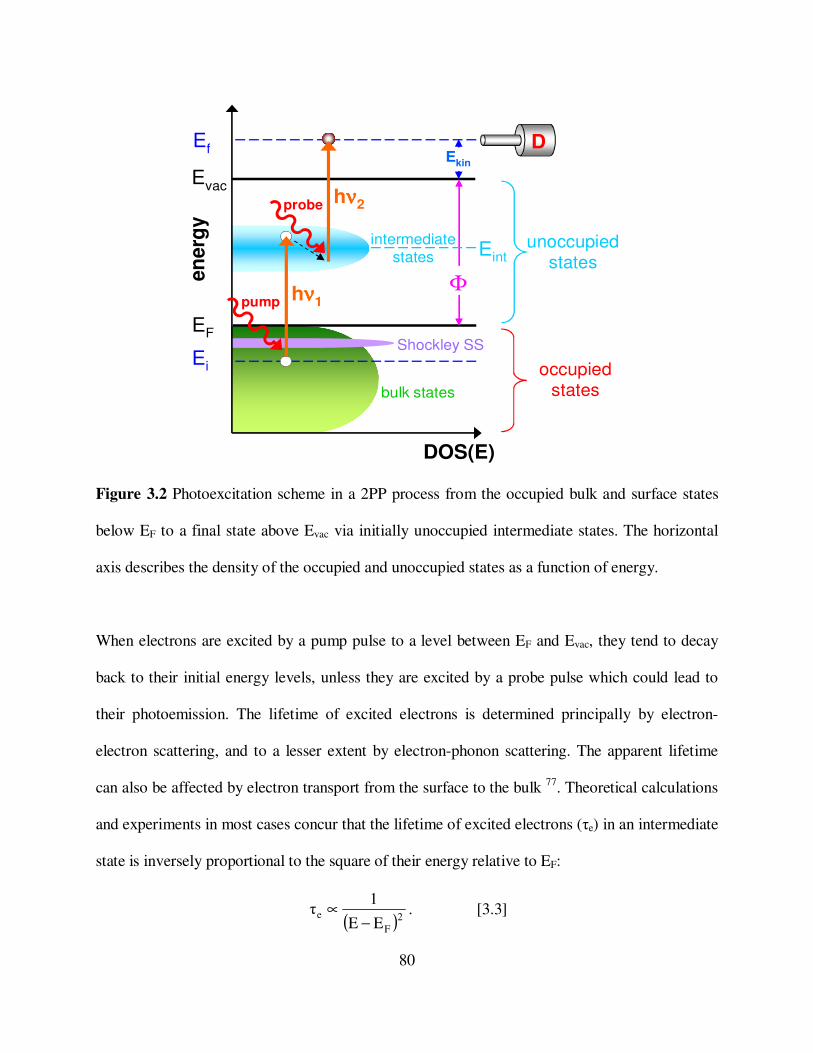
80
Figure 3.2 Photoexcitation scheme in a 2PP process from the occupied bulk and surface states
below EF to a final state above Evac via initially unoccupied intermediate states. The horizontal
axis describes the density of the occupied and unoccupied states as a function of energy.
When electrons are excited by a pump pulse to a level between EF and Evac, they tend to decay
back to their initial energy levels, unless they are excited by a probe pulse which could lead to
their photoemission. The lifetime of excited electrons is determined principally by electron-
electron scattering, and to a lesser extent by electron-phonon scattering. The apparent lifetime
can also be affected by electron transport from the surface to the bulk 77. Theoretical calculations
and experiments in most cases concur that the lifetime of excited electrons (τe) in an intermediate
state is inversely proportional to the square of their energy relative to EF:
( )2F
eEE
1τ
−∝ . [3.3]
Evac
Ef
intermediate states
EF
Ei
Ekin
Φhνννν1pump
probe
DOS(E)
hνννν2
Eint
occupied states
unoccupied states
D
Shockley SS
bulk states
ener
gy

81
Therefore, one can infer that the higher the excited electrons are above EF, the shorter their
lifetime will be 71.
3.2.2 Quantum Mechanical Description of the Excitation Dynamics
The goal of ultrafast laser spectroscopy of solid surfaces is to describe the light–matter
interactions and characterize the dynamics of elementary excitations occurring as a consequence
of photon absorption 80. We employed a semi-classical treatment involving the ‘density matrix’
formalism to explain the coherences and population dynamics, where the electromagnetic field
acts as a classical driving force, while the matter is expressed as a restricted quantized system
composed of several energy levels and a macroscopic heat bath 83. Only the quantum system is
coupled to light, but its phase coherence in strongly affected by its own coupling to the heat bath.
This rendition both leads to a simple explanation of the results in terms of measurable quantities
and accounts for the quantum mechanical aspects of light–matter interaction.
When the excitation pulse width is shorter than or comparable to the phase relaxation time of the
excited medium and the delay between pump and probe pulses is shorter or comparable to the
dynamical change of photo-induced polarization, one needs a theoretical model to formulate the
temporal response of the system, which includes the ‘coherent interaction’ between the
electromagnetic field and the coherent oscillators composing the material. The quantum system
is expressed in terms of its density operator ‘ρ’, which is assumed to obey the ‘optical Bloch
equations’ (OBE). This formulation is developed directly from the Schrödinger equation with a
phenomenological damping term accounting for the coupling with the heat bath:

82
[ ]relax
int0 ρdtd
iρ,HHρdtd
i hh ++= . [3.4]
Here, H0 is the ‘unperturbed Hamiltonian’ of the electronic system and Hint is the Hamiltonian of
the ‘coherent dipolar interaction’ with the electromagnetic field, which acts as a perturbation.
The last term is responsible for the ‘relaxation’ of the excited medium via the coupling with the
heat bath.
Fig. 3.3 shows the excitation scheme for a two-photon excitation in a metallic system. Although
this three-level system is an oversimplification to describe a metal surface 99 , under some
circumstances where there are specific resonances, it is approximately valid. For instance, it can
describe the momentum conserving transitions between the lower and upper sp-band of Ag(111)
that will be discussed in Chapter-4.1 Here, the energy level |0⟩ is an occupied state below EF that
acts as the initial state of the photoexcitation process; |1⟩ is an unoccupied state located between
EF and Evac that acts as the transient intermediate state; and |2⟩ located above Evac corresponds to
a free photoelectron.
Evac
Ef
EF
Ei
Ekin
Φ
Emax
|0⟩⟩⟩⟩
|1⟩⟩⟩⟩
|2⟩⟩⟩⟩
Eint
hν
hν
2hν
122T
012T
11T 02
2T
ener
gy [e
V]

83
Figure 3.3 The photoexcitation scheme for a 2PP process involving three quantized states |0⟩
(initial), |1⟩ (intermediate), and |2⟩ (final) 99. The OBE are employed to describe the interstate
couplings, population dynamics and polarization in a metal. T1 and T2 denote the
phenomenological population and coherence times, respectively.
Consider the material as an ensemble of quantized electronic states defined by unperturbed
Hamiltonian H0 and normalized orthogonal basis vectors |n⟩, such that
nωnEnH n00 h== . [3.5]
The femtosecond laser pulse introduces a time-dependent interaction that couples the eigenstates
of the system:
t)E(t)cos(ωde(t)Edet)(H lωint l⋅⋅−=⋅⋅−=⋅−= Eµ . [3.6]
The new total time-dependent Hamiltonian will be )t(HHH(t) int0 += , and the new wave
function can be written in terms of the basis functions of the unperturbed system
( )∑ −=n
nl nt)(ctinωexpψ(t) , [3.7]
where ωl is the central laser frequency. After solving the time-dependent Schrödinger equation
ψ(t)t
iψ(t)H(t)∂
∂= h , [3.8]
one obtains
( ) ( )
( )( ) ( )[ ]∑
∑
−+−
=
−
∂
∂+−
nlint0n
nlnln
ntinωexpt)(HHt)(ci
ntinωexpt)(ct
inωt)(c
h
. [3.9]

84
If this is multiplied by the complex conjugate of the basis vector n and integrated over the
spatial coordinates, one gets
( ) ( )[ ]∑ −−−−=∂
∂
nnl
mnintmlmm ctωnmiexpH
icmωωic
t h, [3.10]
where the matrix element is ( )ntHmH int*mn
int = .
The density operator ‘ρ’ is defined in terms of the occupation coefficients by n*mmn ccρ = .
According to this formulation, ρmm signifies the population of the level ‘m’, and the off-diagonal
elements ρmn represent the coherences between states ‘m’ and ‘n’. To describe the
interdependence of the density matrix elements, one has to define the population decay times T11
(the population decay at level |1⟩) and T12 (the population decay at level |2⟩); and the first order
decoherence times T201 (between states |0⟩ and |1⟩) and T2
12 (between states |1⟩ and |2⟩); and the
second order decoherence time T202 (between states |0⟩ and |2⟩). Using the derivative of the
product of the occupation coefficients, ( )(t)c(t)ct n
*m ⋅
∂
∂, and the aforementioned decay and
decoherence times, one can construct the OBE to describe the temporal evolution of populations
and polarizations in a three-level quantum system with a set of nine first-order coupled
differential equations 69. The corresponding density matrix can be written as
=
=
2*21
*20
*2
2*11
*10
*1
2*01
*00
*0
222120
121110
020100
cccccc
cccccc
cccccc
ρρρ
ρρρ
ρρρ
ρ(t) . [3.11]

85
Such a scheme will be employed in Chapter-4.1 to model an actual 2PP process on bare Ag(111)
surface, and the OBE will be derived explicitly by means of the equations presented in this
section.
We employ the TR2PP technique to measure the current of free photoelectrons in the final state
at a specific energy. As mentioned above, we measure experimentally the density matrix element
of the final state, ρ22(t,τ), integrated over the pump–probe cycle. Because the laser pulse-to-pulse
( ppT − ) time difference of 11 ns is much longer than the population and coherence times, one can
express the 2PP signal by
( ) ( ) ( )∫∫∞
≅=
p-pT
022
0222PP dtτt,ρdtτt,ρτI . [3.12]
The integral in equation [3.12] is what is measured in a typical 2PP experiment.
3.2.3 Evaluation of Time-Resolved Measurements
I2PC measurements present the nontrivial task of extracting the phase and population decay time
constants. If both are much shorter than the laser pulse, the I2PC measurement resembles an
interferometric autocorrelation (IAC) measured for a medium with an instantaneous response, as
discussed in Chapter-2.1.4 100. If the decay times are finite, I2PC measurements enable us to
extract direct information on the excited electron population and polarization dynamics 71. The
pump laser pulse interacting with the sample surface creates both linear and nonlinear
polarization components, which for resonant excitation oscillate at the excitation frequency ω
and its higher harmonics 100. The interference signal between the pump and probe excited

86
coherences in I2PC scans oscillates at ω and 2ω frequencies. In addition, the excitation process
builds up an incoherent population in the intermediate state through various dephasing processes.
The different contributions to the I2PC scan can be decomposed approximately by Fourier
analysis into 1ω and 2ω components, and a phase averaged component (abbreviated as ‘0ω’),
which evolves on a much longer time scale than the phase of the excitation pulse. The delay-
dependent envelopes of these three components can be computed by Fourier transforming the
experimental I2PC data over each optical cycle as given by
( ) ∫+
−
=
2cλτ
2cλτ
I2PC0ω (t)dtIcλ
τI , [3.13a]
( ) ( ) ( )
21
22cλτ
2cλτ
lI2PC
22cλτ
2cλτ
lI2PC1ω dttω(t)sinIdttω(t)cosIc
2λτI
+
= ∫∫
+
−
+
−
, [3.13b]
( ) ( ) ( )
21
24cλτ
4cλτ
lI2PC
24cλτ
4cλτ
lI2PC2ω dtt2ω(t)sinIdtt2ω(t)cosIc
4λτI
+
= ∫∫
+
−
+
−
. [3.13c]
Fig. 3.4 exhibits an experimental I2PC trace for K/Cu(111) and its decomposition into the 0ω
(blue), 1ω (red), and 2ω (green) components: the measurement is for 2.1 eV intermediate state
energy and at 17° off-normal emission direction.

87
Figure 3.4 Raw experimental I2PC data for K adsorbed on Cu(111) surface (large image)
together with 0ω, 1ω and 2ω component envelopes (inset). The yellow lines show residuals
between the observed (markers) and simulated envelopes (lines). The program for this analysis
was developed by Heberle and Nessler 101,100.
The phase and energy relaxation time constants of the charge carriers within the sample and the
pulse width of the excitation laser pulse govern the temporal profiles of these components.
Assuming that the material response were instantaneous, the electric field of the excitation pulse
would have a Gaussian shape of FWHM of Tp, i.e., ( )( )2pTt4ln2expE(t) −∝ , then the I2PC
signal could be decomposed to 0ω, 1ω and 2ω envelopes 71:
( ) ( )( )2p0ω Tτ4ln2expτI −∝ , [3.14a]
1.0
0.8
0.6
0.4
0.2
0.0
inte
ns
ity
[n
orm
aliz
ed
]
140120100806040200-20-40-60-80
tim e delay [fs]
r aw d a ta 0 ω e n velo pe (p ha se a vg .) 1 ω e n velo pe 2 ω e n velo pe
0 .4 0
0 .3 5
0 .3 0
0 .2 5
0 .2 0
0 .5
0 .4
0 .3
0 .2
0 .1
0 .0
1 00500-50tim e d e la y [fs]
0 .10
0 .08
0 .06
0 .04
0 .02
0 .00
0ω: T11 = 17.8 fs
1ω: T201 = 3.5 fs
2ω: T202 = 1.4 fs
time delay [fs]-80 -60 -40 -20 0 20 40 60 80 100 120 140
raw data0ω envelope (phase avg.)1ω envelope2ω envelope
____________
inte
nsity
[nor
mal
ized
]
inte
nsity
[nor
mal
ized
]

88
( ) ( )( )2p1ω Tτ3ln2expτI −∝ , [3.14b]
( ) ( )( )2p2ω Tτ4ln2expτI −∝ . [3.14c]
Here, I2ω(τ) gives the coherent dephasing time 022T between states |0⟩ and |2⟩; I1ω(τ) gives the
dephasing time 012T between states |0⟩ and |1⟩; and the phase averaged component I0ω(τ) gives
both the coherent polarization and decay time 012T and the incoherent population decay 1
1T of the
intermediate state |1⟩ 78.

89
Chapter-4
Simulation of Two-Photon Photoemission on Ag(111)
This chapter presents 2PP spectroscopic studies of bare Ag(111) surface. This surface is
characterized by simple electronic structure, which makes 2PP spectra amenable to theoretical
analysis. Furthermore, it is a substrate for chemisorption of alkali atoms, therefore, knowing the
clean surface properties is a prerequisite for more advanced studies of adsorbate induced
electronic states. Section 4.1 presents experimental 2PP spectra of Ag(111) surface excited with
3.1 eV light and its simulation based on the bulk band structure of Ag(111), and the optical
Bloch equation simulation of the 2PP excitation process 84. Section 4.2 presents angle-resolved
1PP and 2PP spectra of the same surface and the computation of the angle-dependent dispersion
and 2PP intensities of the sp-band transition.
4.1 Simulation of Two-Photon Photoemission Spectra
The 2PP spectrum of Ag(111) is a good choice for theoretical modeling, because Miller et al.
have developed a corresponding model for the 1PP spectrum that describes quantitatively one-
photon transitions between the same initial and final states 102,103. Their model was based on

90
calculating the optical transition matrix elements using the realistic bulk wave functions and the
Fermi’s golden rule approximation, and accounting for the interference between the bulk and
surface photoemission channels. Because 2PP spectra have never been interpreted quantitatively
based on the known electronic structure of metals, we simulate the 2PP spectra of Ag(111), by
taking Miller’s model 102,103 for 1PP as the starting point for the simulation.
4.1.1 Fundamental Considerations
Besides coupling of the initial and final states as in 1PP spectroscopy, 2PP spectroscopy involves
passage through the resonant or virtual intermediate states. Not only does it provide information
on the densities of the occupied initial and the unoccupied intermediate states, but 2PP spectra
also reveal information on the population dynamics in the transient intermediate states and on
different excitation pathways. The intermediate state dynamics are affected by decoherence of
the direct transitions, excitation through indirect pathways, such as the Drude absorption, and
relaxation phenomena involving electron-electron scattering 84. These dynamical aspects
influence the spectral linewidths and other aspects of photoelectron distributions. Because many
dynamical aspects are difficult to evaluate, a quantitative simulation of 2PP spectra had not been
reported prior to our simulation for Ag(111).
Earlier investigations on 2PP spectral distributions from metal surfaces mostly concentrated on
photoemission involving surface states, such as image potential states 104 and adsorbate-induced
states 55,105, which are localized in energy, because surface normal momentum is undefined or
conserved in the photoemission process 106 , 107 . Unlike surface states with localized energy,

91
photoemission from bulk states involves delocalized bands with surface normal dispersion that
can be calculated or determined by experiment. The transitions are not localized in energy
because perpendicular momentum is not conserved in photoemission.
The 2PP process within the bulk of Ag(111) with 3.1 eV photons takes place across the L-
projected band gap from the (occupied) lower sp-band (Lsp) to the (unoccupied) upper sp-band
(Usp), i.e., spsp LU ← , as shown in Fig. 4.1. The only unoccupied intermediate states of the
correct symmetry to be coupled by p-polarized light and with the same parallel momentum as the
initial states, which are available for photoexcitation in the two-step process, are those of the
upper sp-band 84. The minimum photon energy to excite across the band gap is 4.16 eV, while
the minimum for photoemission through a vertical transition from the lower sp-band is 5.40 eV.
Clearly, the 3.10 eV energy is insufficient for a resonant transition between the lower and upper
sp-bands along the ΓL-direction, and for that matter, elsewhere in the k-space of silver; therefore,
the coherent 2PP process must occur through the virtual excitation of the upper sp-band 108.

92
Figure 4.1 Dispersion of the lower (occupied) and upper sp-bands (unoccupied; abbreviated as
Usp and Lsp, respectively) of Ag along the surface normal (ΓL-direction) and possible resonant
excitation paths for 1PP and 2PP processes with photon energies of 6.0 eV and 3.1 eV,
respectively. The wave number on the horizontal axis is normalized so that the Brillouin zone
boundary corresponds to 1kk L = , at which point the band gap is 4.16 eV. The Shockley surface
state (SS) is located 63 meV below EF 1,3 , and does not disperse along the ΓL-direction.
Electrons excited to the upper sp-band below Evac (‘blue’ region) cannot escape into vacuum.
4.1.2 Experimental Aspects and Implementation
2PP measurements were performed on a single crystal Ag sample that was aligned better than
0.5° along the [111] crystallographic direction and polished to reduce roughness to less than 0.05

93
µm. Before measuring 2PP spectra, the crystal sample was cleaned by successive cycles of Ar+
sputtering (at kinetic energy of 500–600 eV) and high-temperature annealing (at 700–750 K for
45 minutes) under strict UHV conditions (i.e., 10-10 mbar or lower) 84. The number of cycles
required for fresh samples was 30 or more. The overall surface quality of the sample was judged
by two criteria: (1) at the appearance of the LEED pattern and (2) the appearance of the 2PP
spectrum, i.e., minimum inelastic background, maximum work function, and sharp and intense
Shockley surface state. The measurements were performed for sample temperatures between
100–500 K. The sample temperature was controlled by electron bombardment heating and liquid
nitrogen cooling.
The photoemission experiments were performed with the femtosecond laser excitation source
that was introduced in Chapter-2. The 3.1 eV excitation pulses had about 10 fs temporal and
corresponding 200 meV spectral widths. The p-polarized light was incident on the sample at 45°
angle. In addition, we performed 1PP experiments with the fourth harmonic of the Ti:Sapphire
laser. To generate the fourth harmonic, the second harmonic was frequency doubled in another
BBO crystal (of 100 µm thickness). The phase-matching of the BBO crystal permitted doubling
of only the low energy portion of the second harmonic pulse; therefore, the fourth harmonic had
a narrower spectral bandwidth centered around 6.0 eV photon energy.
4.1.3 Experimental Results
Typical, experimentally measured 1PP and 2PP spectra of bare Ag(111) surface with excitation
photon energies of 6.0 eV and 3.1 eV are displayed in Fig. 4.2. The surface normal

94
photoemission spectra are recorded at ~100 K temperature. The spectra show two common
features: (1) the occupied Shockley surface state (SS) 109, which is located within the L-projected
band gap with a binding energy of 0.063 eV below EF (see also Fig. 4.1); and (2) the direct
interband photoexcitation from the lower sp-band to the upper sp-band corresponding to the
peaks located at about 2.11.1 − eV binding energy.
Figure 4.2 1PP (top; with 0.6hν = eV) and 2PP (bottom; with 3.1hν = eV) spectra of clean
Ag(111) surface plotted with respect to the binding energy. The peaks at about 2.11.1 − eV are
due to the direct, resonant photoexcitation spsp LU ← , and the peaks corresponding to 0.063 eV
originate from the Shockley surface state (SS).
x1
03
1.5 1.0 0.5 0.0binding energy [eV]
0
1.5 1.0 0.5 0.0binding energybinding energy [eV]
SS
sp-band 1PP(hν = 6.0 eV)
2PP(hν = 3.1 eV)
ph
oto
emis
sio
n in
ten
sity
[cp
s]
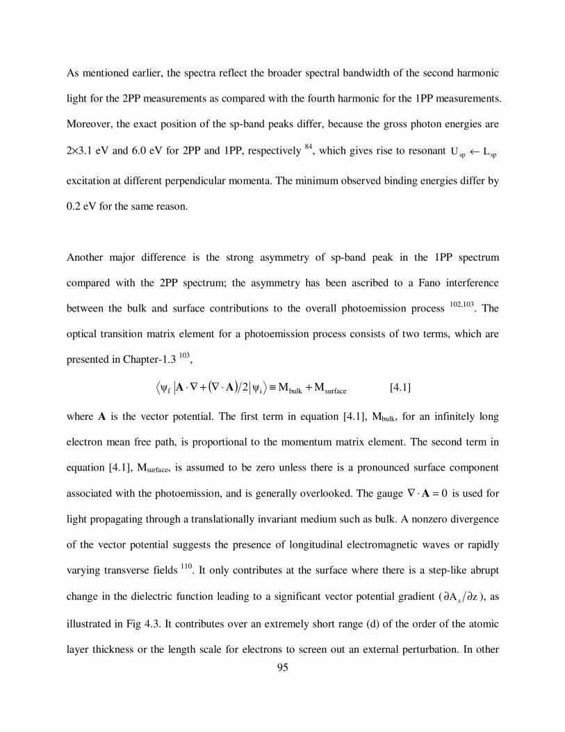
95
As mentioned earlier, the spectra reflect the broader spectral bandwidth of the second harmonic
light for the 2PP measurements as compared with the fourth harmonic for the 1PP measurements.
Moreover, the exact position of the sp-band peaks differ, because the gross photon energies are
2×3.1 eV and 6.0 eV for 2PP and 1PP, respectively 84, which gives rise to resonant spsp LU ←
excitation at different perpendicular momenta. The minimum observed binding energies differ by
0.2 eV for the same reason.
Another major difference is the strong asymmetry of sp-band peak in the 1PP spectrum
compared with the 2PP spectrum; the asymmetry has been ascribed to a Fano interference
between the bulk and surface contributions to the overall photoemission process 102,103. The
optical transition matrix element for a photoemission process consists of two terms, which are
presented in Chapter-1.3 103,
( ) surfacebulkif MMψ2ψ +≡⋅∇+∇⋅ AA [4.1]
where A is the vector potential. The first term in equation [4.1], Mbulk, for an infinitely long
electron mean free path, is proportional to the momentum matrix element. The second term in
equation [4.1], Msurface, is assumed to be zero unless there is a pronounced surface component
associated with the photoemission, and is generally overlooked. The gauge 0=⋅∇ A is used for
light propagating through a translationally invariant medium such as bulk. A nonzero divergence
of the vector potential suggests the presence of longitudinal electromagnetic waves or rapidly
varying transverse fields 110. It only contributes at the surface where there is a step-like abrupt
change in the dielectric function leading to a significant vector potential gradient ( zA z ∂∂ ), as
illustrated in Fig 4.3. It contributes over an extremely short range (d) of the order of the atomic
layer thickness or the length scale for electrons to screen out an external perturbation. In other

96
words, the surface term is related to the difference between the substrate and vacuum dielectric
functions, i.e., 1)ε( − . Because the translational symmetry is broken along the surface normal
(i.e., z-direction) 110, the surface term generates a continuum of momenta. Consequently,
perpendicular momentum in photoemission is not strictly conserved, and therefore, indirect
transitions can occur, producing a continuous distribution of photoelectrons. This surface-
induced indirect background remains phase-correlated with the bulk contribution given by
‘ ∇⋅A ’; their interference is responsible for the asymmetric Fano line shape for the direct (inter
sp-band) transition peak in 1PP spectra. One notices that the line shape of the bulk sp-band
feature in the 2PP spectrum exhibits hardly any asymmetry, implying that the interference
between the bulk and surface components is insignificant. The weaker surface contribution is
consistent with the significantly weaker Shockley surface state peak in 2PP, as compared with
1PP.
Figure 4.3 Bulk–vacuum interface: the discontinuity in the dielectric function at the surface
suggests that its derivative ( zAz ∂∂ ) could be represented by a sharply-defined Gaussian
function, when the range of the surface term ‘d’ is considered to be of the order of an atomic
layer 103.
n(z)
zbulk vacuum
Abulk
Avac
d
zA z
∂
∂+
_

97
4.1.4 Model for Computing the Two-Photon Photoemission Spectrum of Ag(111)
4.1.4.1 Assumptions
Miller et al. modeled the 1PP spectrum of Ag(111) by employing Bloch wave functions for
lower and upper sp-bands within the framework of one-dimensional ‘nearly free electron model’
111 . The transition dipole matrix elements were calculated from electron wave functions
consisting of the Bloch waves for a realistic surface contribution according to the one-step model
of photoemission 3,15,112, where the bulk–vacuum interface was assumed to be a step potential
corresponding to the work function of the Ag(111) crystal surface, as seen in Fig. 4.4. One may
consider the sp-bands within the nearly free electron model, since they form delocalized states,
and their crystal potential, i.e., the electrostatic potential of an ion within a periodic structured
finite crystal 113,114, can be regarded as a weak perturbation. According to this model, the crystal
potential varies sinusoidally along the z-direction. To simulate the 2PP spectrum, we took the
same initial and final state wave functions, and we also had to formulate the intermediate state
wave functions.
z
position w.r.t. surface
bulk vacuum
Vg
V0
Evac
0|p
ote
nti
al e
ner
gy
[eV
]

98
Figure 4.4 ‘The nearly free electron model’ for a sinusoidal crystal potential (Vg) along the
surface normal (z-direction). The surface ( 0z = ) is modeled as an abrupt potential step V0 that
extends from the center of Vg to Evac 15.
In contrast to the 1PP simulation, the 2PP experiment employs a light source with extremely
short duration (~10 fs) and the two-photon absorption process involves excitation and relaxation
dynamics that also occur in the femtosecond regime; therefore, a rate equation approach is
inadequate. For this reason, one needs to use the OBE (not to be confused with the Bloch wave
functions for electrons in a periodic potential), which include the phase and energy relaxation
terms missing in the rate equation approach 69,71,76,80,115.
4.1.4.2 Electron Wave Functions and Transition Matrix Elements
The wave function of the initial state (lower sp-band) in the bulk is composed of a Bloch wave
propagating toward surface and its reflection from the surface propagating in the reverse
direction with an additional reflection-induced phase shift. The phase shift is obtained
quantitatively by matching the Bloch wave with the electron wave function on the vacuum side,
which decays exponentially on account of an imaginary wave vector. The internal and external
wave functions are matched at the ‘image plane’ to be continuous and differentiable at the
matching point. The image plane is estimated at 2.20 a0 (Bohr radius, 0.529a0 = Å 116) in front
of the physical interface or about half an interlayer spacing between consecutive (111)-planes; it
is denoted by z0 117. The wave function matching conditions are
)zz(ψ)zz(ψ 0vac
0bulk === [4.2]

99
00 zz
vac
zz
bulk (z)ψz
(z)ψz == ∂
∂=
∂
∂ . [4.3]
The initial state wave functions are given by
( ){ } ( ){ }zgkizikiqzgkizikbulki
iiii BeAeeBeAe)z(ψ−−−−
+++= , [4.4]
zkvaci
vaciCe)z(ψ
−= , [4.5]
where ( )
h
)k(EΦ2mk iivac
i
−= for 0)k(EΦ ii >− .
All of the wave functions involved in simulating the 2PP spectrum are illustrated in Fig. 4.5.
z [Å]
-40 -30 -20 -10 0 10 20 30
Bloch waves
exponentially decaying
wave
exponentially decaying
Bloch wavesinusoidal
wave
Bloch waves
sinusoidal wave
Bloch waves
exponentially decaying
wave
z0
z [Å]
z [Å]
z [Å]
(a)
(b)
(c)
(d)
bulk vacuum

100
Figure 4.5 Electron wave functions for states involved in the computation of 2PP spectrum of
Ag(111); wave functions for (a) the final state, (b) free (unbounded) electron intermediate state,
(c) bounded electron intermediate state, and (d) initial state.
The final state electron wave function can be thought of as an ‘inverse’ LEED state 102,103,3. To
describe the inverse LEED state, one first needs to model a ‘forward’ LEED state by electrons
incoming as a plane wave propagating from an electron source in the vacuum (the detector in the
‘inverse’ model) to the surface. At the surface, the incoming wave is partially transmitted and
partially reflected according to the complex dielectric function of the surface. Transmitted
electrons give rise to a Bloch wave of the upper sp-band propagating into the bulk, whereas the
reflected part is a plane wave propagating back into vacuum. The transmitted wave is damped by
the inelastic scattering processes, where complex damping wave vector is approximated by the
universal curve 3,15 (Fig. 1.9 in Chapter-1.3). The electron wave functions from both sides are
matched at the image plane as in equations [4.2] and [4.3], in order to obtain the complex
transmission and reflection coefficients. The inverse LEED state wave function can be easily
obtained by reversing the direction of propagation of the forward LEED state throughout. Hence,
the wave function for the final state can be written as
( ){ }zgkizikz/ξbulkf
ff BeAeTe(z)ψ−−−
+= , [4.6]
zikzikvacf
vacf
vacf Ree(z)ψ
−+= , [4.7]
where ( )
h
Φ)k(E2mk ffvac
f−
= for 0Φ)k(E ff >− .

101
In the case of Ag(111), the only available intermediate states for two-photon excitation are the
unoccupied upper sp-band states, which can only function as virtual states. Because the optical
Bloch equations account for the excitation and relaxation of the intermediate states in an
explicitly time-dependent manner, the intermediate sp-band wave functions do not include
lifetime effects as do the final state wave functions, which undergo attenuation. Furthermore,
virtual excitation of Bloch waves propagating in the reverse direction with respect to the detector
is possible, and can contribute to the photoemission process. Thus, the intermediate state wave
functions also include the counter-propagating Bloch waves as do the initial states 84. Although
the majority of the upper sp-band is located above Evac, and therefore, is ‘unbounded’, a small
portion of those states that are adjacent to the Brillouin zone edge are beneath Evac, and therefore,
is ‘bounded’. Hence, the unbounded states are accounted for by matching the wave function from
the bulk to a plane wave in vacuum:
( ){ } ( ){ }zgkizikzgkizikbulkm
mmmm BeAeDBeAe(z)ψ−−−−
+++= , [4.8]
zikvacm
vacmEe(z)ψ = , [4.9]
where ( )
h
Φ)k(E2mk mmvac
m
−= for 0Φ)k(E mm >− .
By contrast, the bounded states are accounted for by matching them to an exponentially decaying
(evanescent) wave function in vacuum:
( ){ } ( ){ }zgkizikiqzgkizikbulkm
mmmmm BeAeeBeAe(z)ψ−−−−
+++= , [4.10]
( )zkFexp(z)ψ vacboundedm,
vacm −= , [4.11]
where ( )
h
)k(EΦ2mk mmvac
boundedm,
−= for 0)k(EΦ mm >− .

102
The aforementioned electron wave functions are employed to calculate the dipole matrix
elements of the first and the second steps of optical transitions within first-order perturbation
approximation as
(z)ψz
(z)ψAψψ~M ijijij∂
∂=∇⋅A , [4.12]
where ‘A’ is the vector potential and ‘z’ is the direction normal to the surface. Indices ‘i’ and ‘j’
denote the initial and intermediate states of the first excitation step, or the intermediate and final
states of the second step, respectively. In terms of the appropriate wave functions for our three-
level system, the optical transition matrix elements are
( ) ( ) ( ) ( )dzz,kψz
z,kψz,kψz,kψd ii
z
m*miim
*m01
0
∫∞−
∂
∂=∇⋅= A , [4.13]
( ) ( ) ( ) ( )dzz,kψz
z,kψz,kψz,kψd mm
z
f*fmmf
*f12
0
∫∞−
∂
∂=∇⋅= A
[4.14]
for the ‘unbounded’ intermediate states; and
( ) ( ) ( ) ( )dzz,kψz
z,kψz,kψz,kψd ii
z
m*
boundedm,iim*
boundedm,bounded01
0
∫∞−
∂
∂=∇⋅= A , [4.15]
( ) ( ) ( ) ( )dzz,kψz
z,kψz,kψz,kψd mboundedm,
z
f*fmboundedm,f
*f
bounded12
0
∫∞−
∂
∂=∇⋅= A [4.16]
for the ‘bounded’ intermediate states. The subscripts ‘01’ and ‘12’ denote the first and second
transition steps in 2PP, respectively.

103
4.1.4.3 Coherence Effects in Two-Photon Photoemission Processes
The complete picture of the photoexcitation processes and the significance of various
computational parameters used in the 2PP simulation are plotted with their energy versus
perpendicular momentum (k⊥⊥⊥⊥) in Fig. 4.6. In the first step, an electron is excited from the initial
state, )k(E ii , on the lower sp-band, to the upper sp-band with the same k⊥ serves as a virtual
intermediate state, because the transition dipole matrix elements obtained from semi-infinite
wave functions of the initial and intermediate states vanish for any mi kk ≠ . In the second
excitation step, violation of conservation of momentum is permitted because k⊥ is not conserved
in the photoemission process. The energy of the final state, )k(E ff , is what is recorded by the
energy analyzer.
8
7
6
5
4
3
2
1
0
-1
-2
-3
E -
E
F [
eV
]
ki
momentum (k⊥⊥⊥⊥)
∆∆∆∆1
Ei
Em
Ef
Ei+2hν
ki=km
EF = 0
Evac
D
kf
hν
hν Lsp
Usp
ener
gy
∆∆∆∆2

104
Figure 4.6 Energy–momentum (k⊥⊥⊥⊥) photoexcitation diagram used for calculating the 2PP
spectrum from Ag(111) including the coherence effects 84. The first step, where the momentum
is conserved, is displayed as a nonresonant excitation from the initial state )k(E ii to the
intermediate state )k(E mm on Usp with energy detuning of ∆1; the second step, where the
absorption of the second photon gives rise to transition to the final state )k(E ff above Evac, is
detuned by ∆2. The number of photoelectrons with respect to their kinetic energy is obtained by
solving the OBE tailored for the energy levels )k(E ii , )kk(E imm = , and )k(E ff ; the spectrum
is obtained by integrating )k(E ff over Lsp.
The photoexcitation scheme outlined in Fig. 4.6 consists of three electronic levels denoted by
)k(E ii , )kk(E imm = , and )k(E ff . Following the scheme presented in Fig. 4.6, one can write
the Hamiltonian of the unperturbed three-level system explicitly as
=
2
1
0
0
E00
0E0
00E
H , [4.17]
where
00 ωE h= , 11 ωE h= , and 22 ωE h= . [4.18]
The time-dependent perturbation term (according to equation [3.6]) due to interaction is
expressed explicitly as
( )
−
−−
−
===
0(t)eEd0
(t)eEd0(t)eEd
0(t)eEd0
tωE(t)cos(t)EH
l
ll
l
l
ω12
ω21ω01
ω10
lωint , [4.19],
where the total Hamiltonian, int0 HHH += , is written as

105
( )
∂
∂=
−
−−
−
=
2
1
0
2
1
0
2ω12
ω211ω01
ω100
a
a
a
ti
(t)a
(t)a
(t)a
E(t)eEd0
(t)eEdE(t)eEd
0(t)eEdE
tψH
l
ll
l
h . [4.20].
When this matrix equation is solved by means of equations [3.10] and [4.18], one obtains a set of
differential equations for the occupation coefficients given by
( ) ( ) ( ) ( )tiωexpteEdtci
tciω(t)ct lω101000 l
−+−=∂
∂
h, [4.21a]
( ) ( ) ( ) ( ) ( ) ( ) ( ) ( )tiωexpteEdtci
tiωexpteEdtci
tcωωi(t)ct lω212lω0101l11 ll
−++−−=∂
∂
hh, [4.21b]
( ) ( ) ( ) ( ) ( )tiωexpteEdtci
tc2ωωi(t)ct lω1212l22 lh
+−−=∂
∂. [4.21c]
The time-dependent excitation and relaxation of these states in response to an ultrashort pulse
laser is calculated by means of OBE, which generate 9 coupled differential equations as
discussed in Chapter-3.2.2 118. Because the off-diagonal elements of the matrix in equation [3.11]
are complex conjugates of each other, however, by symmetry they reduce to 6 equations: (given
as equations [4.22a] through [4.22f])

106
( ) ( ) ( ) ( ){ } ( ) ( ) ( ) ( ){ } ( )
( ) ( ) ( ) ( ){ } ( )
( ) ( ) ( ){ } ( ) ( ) ( )
( ) ( ) ( ){ } ( ) ( ) ( ) ( )
( ) ( ) ( ){ } ( )tρT
1
2T
1i∆tρdtρdtE
2i
tρ
tρT
1
2T
1
2T
1∆∆itρtEd
2i
tρtρtEd2i
tρ
tρT
1
2T
1i∆tρtEd
2i
tρtρtEd2i
tρ
tρ
tρ
t
ρ
T
tρtρtEtρtEd
2i
tρ
T
tρtρtEtρtEd
2i
tρtEtρtEd2i
tρ
20022
21
221011012*20
21122
21
11
1220012211*
1221
10012
11
120121100*
0110
221100
21
2221
*21
*12
22
11
11*21
*211210
*10
*01
11
++−−=∂
∂
+++−−−−=∂
∂
++−+−=∂
∂
∂
∂−
∂
∂−=
∂
∂
−−=∂
∂
−−+−=∂
∂
h
hh
hh
h
hh
.
The photoelectron population of the final state, which is detected by the energy analyzer, is
computed by integrating the OBE within a time frame sufficiently longer than the pulse width of
the laser, where the lifetime of the final state is assumed to be infinite. Then, the population of
the final state is multiplied by the density of the initial ( E)(DOSi ), intermediate ( E)(DOSm ) and
final states ( E)(DOSf ) given by 119
( ) ( ) ( )spsp
L
1
Li Ek
EkE
kEDOS ⊥
−
⊥ ∂
∂=
∂
∂∝ , [4.23a]
( ) ( ) ( ) ( )spsp
U
1
Ufm Ek
EkE
kEDOSEDOS ⊥
−
⊥ ∂
∂=
∂
∂∝= , [4.23b]
which were obtained from the energy band dispersions 120,121.
For any given fixed initial state, the detector energy (i.e., Ef) is scanned over the pertinent final
energy range to obtain )E,E(N ifi . The total calculated 2PP spectrum is obtained integrating the
contribution from each initial state over all the contributing initial states 84:

107
( ) ( )∫=
spLiififtot dEE,ENEN [4.24].
The integral is approximated by a summation over states separated by a sufficiently narrow
energy gap ( 20∆E ≈ meV).
To test the validity of our OBE approach, we input realistic decay times into equations [4.22],
and calculated the time dependent populations. Fig. 4.7 displays the change in the electron
populations in all three states with respect to time. Note that the total number of electrons in the
system remains fixed at all times; the initial state is depopulated rapidly at the time of
photoexcitation, reaching a minimum, and gradually recovering to a depleted value. The final
state population increases rapidly and saturates after the interaction has ceased, because the
lifetime of photoelectrons is assumed to be infinite. The intermediate state population rises and
decays according to the excitation and relaxation mechanisms. The conservation of population in
the three states confirms the validity of our model for describing the excitation and relaxation
dynamics of the three-level system in Fig. 4.6.
-2×10-14
2×10-14
4×10-14
6×10-14
8×10-14
0.2
0.4
0.6
0.8
1
-20 0 20 40 60 80
time [fs]
total
initial
intermediate
finalno
rmal
ized
ele
ctro
n
po
pu
lati
on
0.2
0.4
0.6
0.8
1.0
0.0

108
Figure 4.7 The time evolution of the normalized electron populations in 2PP excitation obtained
by solving the OBE.
4.1.4.4 Temperature-Dependent Background Spectrum
At finite temperatures, electron–phonon interaction gives rise to a continuous contribution of
photoelectrons underlying the k||-conserving 2PP spectral features. Therefore, a complete
description of the experimental 2PP spectra must include both the elastic and inelastic
components. Momentum scattering by phonons can contribute to the 0k || = component of
photoemission through two distinct processes: (1) coherent two-photon absorption accompanied
by phonon absorption or emission; and/or (2) sequential absorption of single photons mediated
by phonon scattering at each step. The sequential process necessarily involves two independent
phonon scattering processes, because there are no resonant transitions from the lower sp-band
that can be excited by 3.1 eV light, as well as no intermediate states at 0k || = for direct k||-
conserving transition to final states above Evac. The latter process is depicted in Fig. 4.8. Because
these higher order indirect processes take place by absorbing or emitting phonons, the inelastic
photoelectron signal should manifest temperature dependence. In agreement with this
expectation, 2PP spectra shown in Fig. 4.8 for temperatures ranging from 100 to 500 K show a
continuous background that increases with temperature, and a shift and broadening of the sp-
band.

109
Figure 4.8 Temperature-dependent 2PP spectra on Ag(111) measured from 100 to 500 K. For
increasing sample temperature, the inelastic electron–phonon interaction increasingly contributes
a continuous background to the 2PP spectra. The temperature-dependent background is evaluated
at energies marked by letters ‘A’ through ‘F’.
If there is substantial quasielastic contribution to 2PP spectra via the second mechanism
involving real population in the intermediate state and the intermediate state lifetimes are shorter
than the laser pulse, the probability of this process should be energy-dependent because of the
( ) 2FEE −
− dependence of electron-electron scattering 122,123,124,125,126. For a decreasing lifetime-
to-pulsewidth ratio, the photoexcited electrons in the intermediate state are less likely to be
excited further owing to competing population decay.
15x103
10
5
0
ph
oto
em
iss
ion
in
ten
sit
y [
cp
s]
1.5 1.0 0.5 0.0binding energy [eV]
100 K 150 K 200 K 250 K 300 K 350 K 400 K 450 K 500 K
0.7 0.8 0.9 1.0
8
6
4
2
0
-2
hν
hν
k⊥⊥⊥⊥
k ≠ k⊥⊥⊥⊥
q
τ
ABCDEF
Evac
EF
q

110
When the optical Bloch equations for this three-level system are solved for the final state
population via phonon-assisted processes by considering the energy dependence of the
intermediate state lifetime in response to 10 fs laser pulse excitation, one obtains a nearly linearly
decreasing photoelectron background as in Fig. 4.9, where the intermediate state lifetime causes
variation in intensity. According to our model, the pulse duration of the excitation laser is a key
factor in determining the amplitude as well as the characteristics of the background. When the
pulse duration is longer than the intermediate state lifetime, the energy dependence of the
phonon-assisted contribution obeys the Fermi liquid theory ( ( ) 2FEE −
−∝ ). When the pulse
duration is noticeably shorter than the hot electron lifetimes, the photoexcitation probability does
not depend on energy and the phonon-assisted contribution attains a nearly energy independent
value. The lack of energy dependence could also be explained by the phonon-assisted two-
photon nonresonant absorption mechanism, which does not require consideration of the
intermediate state lifetime. Because the momentum-integrated density of initial, intermediate and
final states vary slowly with energy 127, the DOS effects are excluded in estimating the phonon-
assisted signal.
15x103
10
5
0
ph
oto
em
issi
on
in
ten
sity
[cp
s]
1.5 1.0 0.5 0.0binding energy [eV]
ABCDEF
2PPT = 250 K

111
Figure 4.9 Experimental 2PP spectrum of Ag(111) at 250 K. The phonon-assisted contribution
extracted from the data in Fig. 4.8 is indicated by the red dashed line. The analysis of the
temperature-dependent phonon-assisted background is shown in Fig. 4.10.
The temperature-dependent background requires interaction of electrons with phonons. The
electron–phonon scattering rate for electrons of energy E and temperature T within the Debye
model is expressed by 3,128,129,130,131
( ) ( )dE')E'(Ef)(E'2f)E'(Ef1EE'
2πTE,ΓDE
0FDBEFD
2
D∫ +++−−
= λ [4.25]
where fFD and fBE are the Fermi-Dirac and the Bose-Einstein distribution functions; ED is the
Debye energy (~19.4 meV for silver 128), and λ is the electron-phonon mass enhancement
parameter. In the energy range above ED, this function is nearly independent of the electron
energy E. The Debye energy is defined as DDBD ωΘkE h== , which corresponds to the crystal’s
highest normal mode of vibration (ΘD: Debye temperature; kB: Boltzmann constant; ωD: Debye
frequency) 132. For temperatures above ΘD, the equation [4.25] can be approximated with a line
of slope of 2πλkB. For temperatures below ΘD, its slope tends to zero and attains a constant value
equal to ( ) DBΘπλk32 . This intercept for 0T = K corresponds to the scattering rate associated
with phonon emission 128. The electron–phonon scattering through phonon emission is
independent of temperature and subsists at all temperatures.
To determine the contribution of Drude absorption, photoelectron intensity for 6 different
energies (indicated by letters ‘A’ through ‘F’ and shown in Figs. 4.8 and 4.9) is calculated and
plotted as a function of temperature in Fig. 4.10. The measurement energies were chosen because
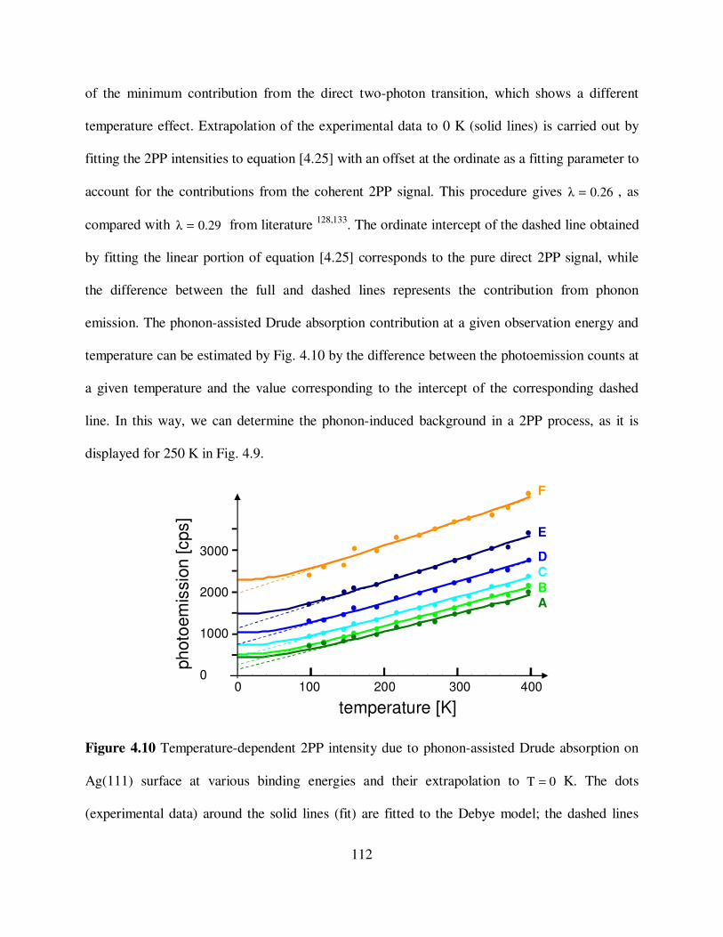
112
of the minimum contribution from the direct two-photon transition, which shows a different
temperature effect. Extrapolation of the experimental data to 0 K (solid lines) is carried out by
fitting the 2PP intensities to equation [4.25] with an offset at the ordinate as a fitting parameter to
account for the contributions from the coherent 2PP signal. This procedure gives 0.26λ = , as
compared with 0.29λ = from literature 128,133. The ordinate intercept of the dashed line obtained
by fitting the linear portion of equation [4.25] corresponds to the pure direct 2PP signal, while
the difference between the full and dashed lines represents the contribution from phonon
emission. The phonon-assisted Drude absorption contribution at a given observation energy and
temperature can be estimated by Fig. 4.10 by the difference between the photoemission counts at
a given temperature and the value corresponding to the intercept of the corresponding dashed
line. In this way, we can determine the phonon-induced background in a 2PP process, as it is
displayed for 250 K in Fig. 4.9.
Figure 4.10 Temperature-dependent 2PP intensity due to phonon-assisted Drude absorption on
Ag(111) surface at various binding energies and their extrapolation to 0T = K. The dots
(experimental data) around the solid lines (fit) are fitted to the Debye model; the dashed lines
100 200 300 4000 100 200 300 400
temperature [K]
3000
2000
1000
0
F
E
DCBA
phot
oem
issi
on [c
ps]

113
show extrapolation of the linear portions for DΘT ≥ to the ordinate. Points ‘A’ through ‘F’ are
indicated in Figs. 4.8 and 4.9.
4.1.4.5 Inelastically Scattered Photoelectrons
Inelastically scattered final state electrons with momentum along the surface normal also
contribute to the background of 2PP spectra. Their contribution is included using the
conventional ‘Shirley function’ 134, in which the inelastic component is given by the integral of
the elastic photoelectrons along the energy axis from the Fermi edge to lower binding energy.
The amplitude of the integral is used as a free parameter to optimize the fit of the experimental
spectrum (see Fig. 4.11(c), the ‘green’ line). The inelastic background augments the overall
intensity particularly in the interval between the sp-band peak and the vacuum edge.
As evidenced in Fig. 4.2, both 1PP and 2PP should have comparable contributions from the
inelastically scattered photoelectrons (Shirley background), which depend on the final state
energy distribution rather than the excitation process 134. Assuming that the background signal at
the vacuum edge in both cases is composed of inelastically scattered photoelectrons, one can
compare their intensity and check for consistency. This test shows that the 2PP background is
about 1.8 times larger than that of 1PP. The elevated background for 2PP suggests that there
could be an additional contribution to the 2PP signal near the vacuum edge. Studies of 2PP on
rough Ag films demonstrated that there exists an additional 2PP excitation pathway linked to the
excitation of local surface plasmons at roughness features 108. Another experiment conducted on
the same Ag(111) surface by a photoemission electron microscope (PEEM) reveals that such

114
roughness features exist and give rise to intense photoemission signals (‘hot spots’) mediated by
surface plasmons 135. Nonetheless, the photoemission contribution from these surface plasmons
makes a minor contribution to the overall photoemission yield.
4.1.4.6 Total Two-Photon Photoemission Spectral Distribution
Fig 4.11 presents all of the contributions to the 2PP signal obtained in the computations of
section 4.1 and comparison of their sum with the experimental 2PP spectra. The three major
elements contributing to the 2PP spectrum in the order of significance are the coherent 2PP (Fig.
4.11(d)), incoherent Drude absorption (Fig. 4.11(b)), and inelastic electron background (Fig.
4.11(c)). The Shockley surface state (shown in Fig. 4.11(a)) is assumed to be a Gaussian function
centered at 0.063 eV binding energy. It is added by hand, since the relative surface and bulk 2PP
contributions are not known. The direct coherent 2PP signal has a peak at about 1.2 eV initial
state binding energy corresponding to the energy conserving resonant two-photon excitation
between the lower sp-band to the upper sp-band by 400 nm wavelength laser pulse (Fig. 4.11(d)).
This peak displays a slight asymmetry, which we attribute to decreasing surface transmittance
probability of the low kinetic energy photoelectrons 108,136. The surface transmittance, which is
also known as the ‘escape function’, modulates the pure photoexcitation probability of bulk
electrons. In this study, it is obtained from the surface transmission coefficient of the final state
electron wave function and by matching the vacuum and bulk sides of the wave function at the
image plane. A substantial change in the surface transmittance of an intrinsically symmetric
spectral distribution gives rise to discernible asymmetry (and minor consequent augmentation in
intensity) for the transmitted electrons on the lower binding energy side.

115
Figure 4.11 Contributions to 2PP spectrum from Ag(111) surface at 100 K, and the comparison
of the experimental data with the aggregate simulated contributions. (a) Shockley SS is assumed
to possess a Gaussian shape. (b) Phonon-induced background depends on temperature and
exhibits a nearly linear behavior decreasing toward lower binding energy. (c) Shirley background
is approximated as an integral of elastic electrons from the Fermi edge to lower binding energy.
(d) The direct coherent 2PP signal shows slight asymmetry caused by the escape function (dotted
line). (e) Aggregate of all components (red line) and comparison with the experimental data
(gray circles).
(a) Shockley SS
(b) phonon-induced
(c) Shirley
(d) direct
simulation
experiment
__
o
(e) total
binding energy [eV]1.5 1.0 0.5 0.0
0.0
0.5
escape function
phot
oem
issi
on in
tens
ity [c
ps] (×
103 )

116
In the absence of an actual intermediate state in the sp-band gap of Ag(111), the continuum of
the upper sp-band serves as the virtual intermediate states, while the energetically more favorable
image potential states (n = 1, 2, 3, etc.), which are located about 0.77 eV below Evac 62,137, appear
not to be involved in the 2PP mechanism of the bulk states. If the image potential states were to
engage, they would introduce a surface-mediated excitation channel that could interfere with the
bulk excitation channel. As mentioned earlier, the considerably smaller asymmetry of the bulk
bands in 2PP, as compared with the 1PP spectra, argues against the surface channel having a
significant contribution. The Shockley surface state intensity difference between the 2PP and
1PP spectra confirms that the surface excitation channel is less prominent in the 2PP process.
Because the initial and final states are in principle the same for the 2PP and 1PP processes, the
difference between the surface versus bulk photoemission in the linear and nonlinear excitation
must arise from different surface and bulk transition moments involving the intermediate states.
According to the band structure of Ag(111), it is clear that the upper sp-band states above Evac
are available as final states only for (the ‘white’ zone in Fig. 4.1), which is far
from the Brillouin zone edge. Not even does the penetration of the image potential states due to
imaginary momentum within the band gap enable them to be effective virtual intermediate states.
Nevertheless, one can expect them to be effective virtual intermediate states for 2PP from the
Shockley surface state, which was studied for Cu(111) 104.
Although the entire 2PP process on Ag(111) surface involves continuous energy bands, the OBE
model is implemented by considering discrete states of a three-level system with a single
intermediate state, which corresponds to the upper sp-band at the same k⊥⊥⊥⊥ as the initial state. The
ΓL0.89kk ≤⊥

117
simulation of 2PP spectra of Ag(111) shows that in the case that band-to-band transitions are
localized in k-space, it is possible to reproduce the spectra based on relatively simple models that
are grounded in conventional theory of 1PP. For 2PP the dynamical processes in metals in
addition to the coherence properties of the excitation source play an enhanced role. Ag(111) is an
ideal case for simulation because there is substantive theoretical ground work from previous 1PP
studies, and the lack of real intermediate states diminishes the role of electron scattering effects.
Although Cu(111) has a similar band structure, its spectra with the same photon energy are
almost featureless obviating description by models such as presented here. The difference may
arise from the proximity of the d-bands to EF, which provides additional indirect channels for hot
electron excitation 138,139.
4.2 Angle-Resolved Two-Photon Photoemission from the sp-Bands of Ag(111)
4.2.1 Introduction
Using the ARPES technique, one can obtain information about the electronic band structure by
analyzing the observed dispersion of peak positions in photoemission spectra. As a model system
for quantitative analysis of the photoemission mechanism and spectra, the bulk band structure of
silver has been widely investigated by ARPES 84,140,141,142. In terms of analyzing the relative
intensity information of angle-resolved photoemission studies, the role of the polarization of the
incident light was studied experimentally and theoretically 143,144,145, and the relationship between
the momentum matrix elements and the measured intensities of energy-dependent transitions was
also described 146. In the photon energy range relevant to our study, considerable interference

118
between the surface and bulk photoemission has been observed in the surface normal 1PP spectra
of Ag(111) surfaces 102,103.
We have performed both angle-resolved one-photon photoemission (AR1PP) and two-photon
photoemission (AR2PP) experiments on bare Ag(111) surface. The two-photon transition
between the lower and upper sp-band described and analyzed in the previous section provides an
opportunity to examine whether theory can also account for the differences in the angle-
dependent intensities between the AR1PP and AR2PP spectra of Ag(111), to be described in this
section. We explain the angle-dependent intensity variation observed in AR2PP experiments
within the framework of Fresnel equations, in the case where additional effects such as surface
photoemission are negligible. We also examine how refraction suffered by low-energy
photoelectrons at the metal–vacuum interface affects quantitative band structure mapping. We
find that low energy photoelectrons of a well-defined direct optical interband transition can
provide accurate information on the inner potential 147. After accounting for the refraction effects,
the observed dispersion of the sp-band transition of Ag(111) can be simulated by a nearly free
electron model for the initial and final states. The measured sp-band dispersion agrees with the
known band structure.
4.2.2 Experimental Details
The angle-resolved measurements were performed by rotating the angle of the sample with
respect to the laser incidence and photoelectron analyzer axes, which were fixed with respect to
each other at an angle of 45°. Fig. 4.12 defines the relevant angles for the angle-resolved

119
photoemission measurements. The experiment was started with the incident laser beam with p-
polarization at 45° angle with respect to the sample normal. After the acquisition of repetitive
spectra was started, after each scan the sample was turned back and forth in 1° increments by
rotating the sample manipulator about the perpendicular axis to the optical plane.
Figure 4.12 The geometry used in angle-resolved photoemission experiments. The angle
between the incident light (laser beam) and the detected electrons (energy analyzer) is fixed to
°=+ 45θθ Di . Ai and AT stand for vector potentials for ‘incident’ and ‘transmitted’ light. The
photoelectrons leaving the surface with θD propagate inside the solid with an angle θint.
4.2.3 Experimental Results
Angle-dependent 1PP and 2PP experiments in Fig. 4.13 were carried out on a cleaned and
annealed Ag(111) surface with p-polarized incident light. Dispersing spectral features due to the
bulk sp-band transition and the Shockley surface state are evident. The surface state disperses
vacuum
solid
z
θi
θD
θint
Ai
AT
Ekin
incident laser

120
above EF within several degrees from the surface normal (red dashed line), where it can no
longer be observed. The dispersions of the sp-band transition in both 1PP and 2PP measurements,
however, are observable over an extended range of angles before the lower sp-band disperses
above EF. The intensity distribution of the bulk transition in the AR2PP spectra is conspicuously
asymmetric, whereas the AR1PP appears symmetric with respect to the surface normal. As in Fig.
4.2, the Shockley surface state has higher (lower) photoemission intensity relative to the sp-band
peak because of different surface and bulk contributions, and has a narrower (broader) spectral
width in AR1PP (AR2PP) because of the phase matching limitations of the BBO crystal.
-30
-20
-10
0
10
20
30
emis
sion
ang
le [d
eg]
1.5 1.0 0.5 0.0binding energy [eV]
-30
-20
-10
0
10
20
30
emis
sion
ang
le [d
eg]
1.5 1.0 0.5 0.0binding energy [eV]
(a) AR1PP
(b) AR2PP
AR
1PP
intensity [cps]
AR
2PP
intensity [cps]
emis
sio
n a
ng
le [
deg
]em
issi
on
an
gle
[d
eg]
binding energy [eV]

121
Figure 4.13 Experimental (a) AR1PP ( eV) and (b) AR2PP ( eV)
measurements. The dashed horizontal lines indicate the surface normal emission angle. The
AR2PP intensity angular distribution is conspicuously asymmetric with respect to the surface
normal, whereas the AR1PP intensity distribution appears nearly symmetric.
4.2.4 Theoretical Modeling
4.2.4.1 Dispersion of the sp-Band Transition Peaks
In order to account for the differences between the AR1PP and AR2PP spectra, in Fig. 4.14 we
present a three dimensional k-space representation of the lower and upper sp-bands and illustrate
the possible photoexcitation pathways. The sp-band gap width at the L-point is 4.16 eV 84,
whereas the lower sp-band maximum at 0k || = occurs at -0.30 eV 147.
6.0hν = 1.3hν =

122
Figure 4.14 Three-dimensional illustration of the nearly free electron band structure for the
lower and upper sp-bands involved in the direct two-photon transition for Ag(111). The zero of
the energy scale is set at the bottom of the lower sp-band. The lower sp-band is filled up to EF, as
indicated by the black shading. The internal emission angle of electrons is denoted by θint.
Direct photoexcitation occurs in the momentum space where the difference between the initial
and final state energies equals the 1PP photon energy or twice the 2PP photon energy. The
resonance condition determines the perpendicular and parallel components of k participating in
the excitation and consequently the internal angle inside the solid (θint) prior to emission.

123
As described in Fig. 1.11, for an electron to be emitted, it must overcome a surface potential
barrier ( 0EEV 0vacR >−= ), which corresponds to the energy difference between Evac and the
band origin (E0) given by the nearly free electron model. Since the kinetic energy of
photoelectrons is measured relative to Evac, the electrons inside the solid have energy of
. The potential step at the interface corresponding to VR causes refraction of electrons
such that energetic electrons inside the solid with an angle ‘θint’ emerge into vacuum at an angle
‘θD’; the internal and external angles are related by 3
21
kin
Rkin
int
D
EVE
sinθsinθ
+= , [4.26]
as well as implicitly by equation [1.12]. According to this simple model, the dispersion of the sp-
band transition is governed by several parameters: the minimum of the upper sp-band and the
maximum of the lower sp-band at 0k || = , Evac, and EF. Obviously, we expect this model to
remain valid within a limited range of k||, because of deviations of the actual band structure from
the nearly free electron model.
4.2.4.2 The Angular Photoemission Intensity Distribution
As introduced in Chapter-1.3, 1PP process can be described by first-order perturbation theory
through a Fermi’s golden rule approximation to describe how an electromagnetic field interacts
with atoms of a solid. The corresponding photocurrent in 1PP process can be expressed by
equation [1.9] as
. [4.27]
Rkin VE +
( ) ( )
( )hνEEδM
hνEEδψHψEI
if2
if
if2
iintf1PP
f
−−=
−−∝

124
After evaluating the integral within the absolute value sign, the matrix element between the
initial and final states can be expressed as
, [4.28]
where Pif is the momentum matrix element and the photocurrent of 1PP can be simplified as
( ) Θ∝⋅∝ 221PPf cosEI ifPA , [4.29]
which shows a proportionality between the 1PP intensity and the square of the matrix element.
The 2PP intensity can be expressed through second-order time-dependent perturbation theory as
a sum over all possible intermediate states ‘m’:
. [4.30]
For the observed transition in Ag(111), there are no resonant intermediate states, as explained in
section 4.1 for the normal emission. In the case of nonresonant excitation between bands of the
nearly free electron two-band model, the square of the product of the matrix elements in equation
[4.30] can be expressed as
, [4.31]
where Θ is the angle between A and Peff, the effective momentum matrix element of the 2PP
process (only the angle is important). The 2PP photocurrent is then proportional to
( ) ΘcosEI 442PPf ∝⋅∝ effPA . [4.32]
ifPArA ⋅=∇⋅= ifif ψ)(ψ2mcie
Mh
( ) ( )hν2EEδhνEE
ψHψψHψEI if
2
m im
iintmmintf2PPf −−
−−∝ ∑
ΘcosMM 42
mf*im ∝

125
The momentum matrix elements Pif (for 1PP) and Peff (for 2PP) are in general complex vectors
with amplitudes that need not be explicitly calculated to determine that angle dependence of 1PP
and 2PP 148.
From the above formulation, the measured angle-dependent intensities originate from two main
factors. First, the electric field vector changes in the solid with the angle of incident laser beam.
This phenomenon is described by the Fresnel equations in classical optics, as it quantitatively
describes the direction, magnitude, and relative phase of the vector potential, and consequently,
the transmission and reflection coefficients at the solid–vacuum interface 149,150. Second, the
coupling of the vector potential A of the incident light to the electronic system leads to an angle-
dependent probability of photoelectron detection in the direction of the electron analyzer, as
expressed in equations [4.29], [4.31], and [4.32].
The photoelectron yield in photoemission, regardless of the direction of electron emission, is
proportional to the total energy deposited on the sample surface. The deposited energy is
proportional to , where ‘R’ is the reflectivity of the sample in response to the s- or p-
polarized light and ‘n’ denotes the order of the photoemission process. For p-polarized light, the
photoemission intensity increases near the pseudo-Brewster’s angle, where the reflectivity is
minimum and the transmission is maximum.
In angle-resolved photoemission, the transition matrix element is largely controlled by the
relative orientation of the vector potential AT and the photoelectron momentum Pif, as indicated
in equation [4.32]. These effects are separately described in equation [4.28] by the vector
( )nR1−

126
potential A and the momentum matrix element Pif, which depends on the angle of the emitted
final state photoelectron. This angle is fixed with respect to the incident beam in our experiment.
The variation in the z-component of AT is the dominant contribution to the photoemission
intensity for p-polarized incident light. The term ‘ A⋅∇ ’ in equation [1.7] is nonvanishing at the
surface due to the dielectric discontinuity. This surface contribution to the transition matrix
element for photoemission can be approximated by 103,151
+⋅≡+∝
2dC
∆AMMM zsurfacebulkif ifT PA , [4.33]
where ‘C’ is a complex fitting parameter. The change in the z-component of A (∆Az) in
transition from vacuum into the solid through an effective depth ‘d’, which is of the order of
interatomic distance is given by 147,151,152
, [4.34]
which can be calculated by the Fresnel equations. Apart from the surface photoemission, several
other processes could also impact the angle-resolved photoemission intensity. Photoexcited
electrons traveling from a certain depth within the solid toward the solid-vacuum interface with
larger angles relative to the surface normal are more likely to undergo inelastic scattering,
because they propagate over longer distance within the solid 147. Moreover, the photoemission
peak shapes will depend on the varying k-space resolution with the exit angle, which is caused
by refraction. These factors can be seen at exit angles of 30° or more and are symmetric with
respect to the surface normal 147.
−
−+= i
i2
i
iiz sinθ
θsinεεcosθ
sinθ2cosθ∆A iA

127
Our model employs the Fresnel equations to deduce the refracted vector potential AT as a
function of the incident vector potential Ai for the known dielectric function of Ag 153,154:
. [4.35]
If the dipole matrix element for the observed transition is directed along the surface normal, the
photoemission intensity is determined by the z-component of the vector potential outside the
metal and given by 153,154
. [4.36]
The variation of Az as a function of angle of incidence is nearly independent of the photon
energy (within or around the energy range that we use) and whether we look at silver or copper
147. Therefore, our results can be generalized to a wide variety of materials and at the
aforementioned photon energies.
The momentum matrix element Pif, is a complex vector that depends on the initial and final
states in the photoemission process. In general, it is also a function of the wave vector of the
emerging photoelectrons. Studying the momentum matrix element can potentially reveal
information on the wave functions of the states involved and their symmetry 155. Our model
assumes that the momentum matrix element points in the direction of the surface normal and the
z-component of the vector potential inside the solid is a critical factor for the overall angle-
dependence of the photoemission intensity for p-polarized incident light.
Combining these effects by the results shown in equations [4.29] and [4.32], the general behavior
for the angle-dependent intensity of sp-band transition spectra can be formulated as
ε(ω)
( )ε(ω)),(θiiTT AAA =
i2
i
iiz
θsinεεcosθ
sinθ2cosθA
−+=
iA

128
, [4.37]
where ‘n’ denotes the order of the photoemission process 147. Fig. 4.15 shows the angle-resolved
intensity variation computed with the above formula as a function of the angle of incident light
for 1PP and 2PP, where they designate the square and the fourth power of Az, respectively.
Figure 4.15 Angle-resolved photoemission intensity variation computed by for the
(1PP) and (2PP) cases. The 45° angle of incidence (red dashed line) signifies the 0°
(normal) emission angle for photoelectrons.
Because we applied 2 V of bias voltage to our sample, some deflection occurs on the
photoelectron trajectories for off-normal directions. The deflection increases at larger exit angles.
To quantify this effect, we calculated the apparent effective mass (meff) of photoelectrons for the
Shockley surface state of Cu(111), which produced 0.30mm eeff = ; this is less than what has
been reported in the literature, i.e., 156,157,3. This means that the applied
bias voltage enhances the effective dispersion and restricts the accessible k-space.
( ) ( )( ) 2nziz
nPPf Pωε,θAEI ⋅∝
1.0
0.8
0.6
0.4
0.2
0.0
(nor
mal
ized
inte
nsity
[cps
])
|Az
• P
z|2n
9080706050403020100angle of incidence [deg]
AR2PP: hν = 3.1 eV AR1PP: hν = 6.0 eV
2n
zz PA ⋅
1n = 2n =
45.040.0mm eeff −=

129
The k||-dispersion of the transition energy between the initial and final states for the direct
photoexcitation is amplified by refraction at the solid-vacuum interface. The best agreement
between experiments and our simulation is found for an inner potential 5ΦVV R0 =−= eV
after correcting for the bias voltage-induced deflection by the effective mass of the Shockley
surface state. Inner potentials of 4.0 eV 158, 5.0 eV 159, and 6.7 eV 160 reported elsewhere are very
close to our findings. The reason for the ambiguity of the inner potentials stems from the
intermixing of the lower sp-band and the d-bands of Ag(111) as well as using different models to
calculate them. Considering these factors, one can conclude that there exists sizable uncertainty
in the exact value of the potential step that leads to refraction, especially at very low energies as
in 2PP measurements. This uncertainty could be of minor significance for band mapping in
ARPES experiments with high photon energy; the error in the exit angles at low electron
energies that is caused by the uncertainty in the inner potential, however, will overwhelm the
effects caused by the band structure. If we reverse this assumption and suppose that the sp-band
structure is sufficiently well-known from high energy ARPES experiments, we have a sensitive
probe for the inner potential in the form of the refraction of very low-energy photoelectrons 147.
Thus, the measurement of the inner potential could be calibrated against sp-band photoexcitation
that is well-defined in k-space. The information imparted by the inner potential is of paramount
importance for the analysis of spectroscopic and imaging methods where low energy
photoelectrons are employed such as LEED and PEEM 161.
Fig. 4.16 presents simple simulations of the refraction through the solid-vacuum interface for
different kinetic energies (Ekin) and potential barriers (VR). One can see that nearly all
130
photoelectrons originate from a cone of half opening angle of about 10° within the sample for the
kinetic energy range in our experiments. This effect indicates that the detected region within the
k-space is narrow. It, nevertheless, does not preclude band mapping of bulk bands of solids by
AR2PP. With photon energies available for 2PP experiments (up to eV) and wide
detection angles (up to ), it is still possible to acquire substantial information (up to
) on the dispersion of the parallel wave vector components 147.
Figure 4.16 Refraction of photoelectrons through the solid-vacuum interface reduces the range
of angles of electrons that can emerge from the solid.
According to our model formulated in equation [4.37] and shown in Fig. 4.15, angle-dependent
distributions of photoelectrons from both 1PP and 2PP should be asymmetric with respect to the
surface normal, and because of its higher order in light intensity the AR2PP distribution should
be narrower than the AR1PP distribution. Once the data presented in Fig. 4.13 are translated into
normalized photoemission intensity as a function of emission (detection) angle, as demonstrated
4Ekin ≈
oD 70θ ≈
oint 30θ ≈
25
20
15
10
5
0
angl
e in
side
sol
id [d
eg]
9080706050403020100
(exit) angle outside solid [deg]
Ekin = 0.5 eV; VR = 6 eV Ekin = 1.0 eV; VR = 6 eV Ekin = 1.5 eV; VR = 6 eV Ekin = 1.0 eV; VR = 8 eV Ekin = 1.0 eV; VR = 10 eV

131
in Fig. 4.17, one notices that the model for AR2PP agrees very well with the data, whereas the
data from AR1PP do not fit the simple Fresnel model. The relative deviation of the AR2PP data
from the model at large negative exit angles (Fig. 4.17) can be ascribed to the unavoidable
uncertainty in extracting the intensity sp-band transition peaks from a large background. This can
also be seen at very low photoemission intensity at very large negative angles as shown in Fig.
4.13(b). To validate the model for both the 1PP and 2PP cases, Winkelmann 147 also compared
the angle-dependence of the intensity of electrons excited from near the Fermi edge of Cu(001)
in AR1PP and AR2PP spectra excited with comparable photon energies as for Ag(111). The
Cu(001) intensities in both linear and nonlinear spectra agreed with our model based on Fresnel
equations for the angle-dependent intensities. The ability of our model to predict the angle-
dependent intensity distributions of AR2PP spectra from Ag(111) and AR1PP and AR2PP
spectra of Cu(001) indicates that it can be generalized to other substrates. The AR1PP angular
distributions for Ag(111) remain the exception.
1.0
0.8
0.6
0.4
0.2
0.0norm
aliz
ed p
hoto
emis
sion
inte
nsity
[arb
. u.]
-40 -30 -20 -10 0 10 20 30 40emission (detection) angle [deg]
AR2PP data: Ag(111) AR1PP data: Ag(111) AR2PP data: Cu(001) AR1PP data: Cu(001) AR2PP model: Ag(111) AR1PP model: Ag(111) AR2PP model: Cu(001) AR1PP model: Cu(001)
132
Figure 4.17 Normalized intensities of AR1PP (with eV) and AR2PP (with
eV) experimental data taken for Ag(111) and Cu(001) surfaces and their comparison with our
model based on the Fresnel equations. The calculations reproduce the experiments well except
for the AR1PP of Ag(111). We attribute the discrepancy to interference with the surface
photoemission, which is not accounted for in our model.
To scrutinize the origin of the anomalous AR1PP intensities for Ag(111), in Fig. 4.18 we
compared the 2PP and 1PP spectra recorded at +20° and -20° from the surface normal. The sp-
band transition peaks in 1PP are more asymmetric than those of 2PP. The peak-to-background
intensity ratios in 2PP spectra remain nearly constant, while for 1PP high sp-band intensity at
negative angles is associated with a low background, while at positive angles low peak intensity
is associated with a high background. We attribute these anomalies, along with the strongly
asymmetric line shapes, to the interference between the surface and bulk photoemission channels,
which is well documented for the Ag(111) surface 102,103. Because the p-component of the
excitation light increases at large positive angles, the surface component corresponding to the
background emission is enhanced; the fact that the bulk component does not follow the
expectation from the Fresnel equation model suggests that the direct bulk transition is suppressed
by destructive interference with the surface photoemission.
6.0hν = 1.3hν =

133
Figure 4.18 AR1PP and AR2PP spectra taken on Ag(111) surface at large angles from the
surface normal (+20° and -20°) are juxtaposed to contrast the anomalous behavior of the 1PP
data, which is attributed to the interference between the surface and bulk photoemission.
Therefore, we conclude that our model for the angle-dependent intensities accounts accurately
for the bulk photoemission as long as the surface component is weak. In the case of AR1PP
spectra of Ag(111), a strong surface contribution interferes with the bulk contribution in an
angle-dependent manner, precluding analysis with our model based on Fresnel equations.
Despite the approximations made, we have shown that it is possible to understand and model the
electronic structure and nonlinear two-photon excitation processes at metal surfaces by means of
AR2PP experiments 147.
phot
oem
issi
on in
tens
ity [a
rb. u
.]
1.5 1.0 0.5 0.0binding energy [eV]
2PPE
Ag(111)AR2PP Ag(111)
+200
-200
1.5 1.0 0.5 0.0binding energy [eV]
1PPE
Ag(111)AR1PPAg(111)
+200
-200

134
Chapter-5
The Electronic Structure of Chemisorbed Alkali Atoms on Noble
Metal Surfaces
As already discussed in Chapter-1, atoms and molecules can interact with surfaces through
physical or chemical forces. Alkali atoms are strongly chemisorbed; at low coverage, they donate
their valence s-orbital electron to the substrate, and exist in essentially ionic state. There are no
spectroscopic features of this ionic bond in the valence state spectra of alkali atom modified
metal surfaces. In this chapter, we explore systematically the unoccupied electronic structure of
Li through Cs on Cu(111) and Ag(111) surfaces by photoinduced charge transfer excitation
mediated 2PP spectra.
When an atom with discrete energy levels is brought into close contact with a metal substrate,
which is characterized by a large electron density (~1023 per cm3) 16, the unperturbed ground
state energy levels of the atom interact with the continuum of metallic states 162. Electrons in the
metal are polarized by the external charges. Consequently, the energies of the atomic states shift
in response to the induced potential, and broaden into a resonance due to the possibility of
tunneling into and out of the continuum of electronic states of the substrate 38. When electrons

135
tunnel out of singly occupied s-orbitals of atoms such as alkali atoms and are delocalized within
the conduction band of the substrate, they leave a positively charged ion on the surface.
Fig. 5.1 illustrates the polarization of electrons in the metal by the external positive and negative
charges of an alkali atom. The screening of the external charges induces fictitious image charges
of opposite sign and equally distant, but on the opposing side of a fictitious image plane. The
distance between the center of the adsorbate atom and the image plane along the z-axis at
equilibrium is defined as the ‘adsorption height’ (Rads). The attractive interaction between the
ionic alkali atom core and the substrate is responsible for the strong chemisorption (~2 eV
binding energy) of alkali atoms. The repulsive interaction between the ns valence electron of
alkali atom and the negative image charge of the ionic alkali atom core destabilizes the valence
state above EF, whereby it becomes an unoccupied resonance.
Figure 5.1 Alkali atom adsorption on noble metal surface at chemisorption distance (Rads) leads
to formation of the image charges and their interactions with one another. VIP stands for the
attractive image potential and V∆ denotes the repulsive image-charge potential 163.
+
_
_+
Rads
ρ
ns-electron
alkali atomimage charges
net repulsion
metal surface
VIP
V∆

136
Noble metals are characterized by electronic structures consisting of sp-band electrons at EF with
slowly varying DOS and fully occupied d-bands several eV below EF 33. The sp-bands have
structureless, slowly varying DOS distribution in the energy range of our experiments. Alkali
atoms have simple electronic structures with one valence electron and low ionization potential.
Therefore, alkali atoms form a very simple chemisorption system on noble metal surfaces where
any change in the occupied and unoccupied electronic structure of the noble metal due to alkali
atom adsorption becomes easy to discern.
Historically, there have been several chemisorption models to explain the alkali metal
chemisorption 164. We mainly consider (1) the Langmuir-Gurney model, and (2) the Muscat-
Newns model, which are schematically displayed in Fig. 5.2. According to the Langmuir-Gurney
model, when the ns valence electron of an alkali atom approaches a metal surface, it is repelled
by the positive core-induced image charge within the metal, as shown in Fig. 5.1 21,38,12. Beyond
a certain distance where the ns orbital crosses above EF, electron tunneling into the unoccupied
states of the metal becomes energetically feasible. At the equilibrium chemisorption distance Rads,
the ns orbital shifts a few eV upward owing to the Coulomb repulsion; the resonance bandwidth
in the Langmuir-Gurney model is several eV because of facile tunneling into the conduction
band of the substrate. While there is very low alkali atom coverage on the metal, the adsorbate
atoms are nearly completely ionized, because only a small portion of the total ns state is
occupied, as graphically depicted in Fig. 5.2(a). This model qualitatively agrees with the
measured work function change curves as a function of alkali atom coverage; it has been
generally accepted that the Langmuir-Gurney model describes the basic components of the alkali

137
atom chemisorption 20. Later Gadzuk cast the Langmuir-Gurney model for alkali atom
chemisorption within the Anderson impurity model 165.
Figure 5.2 Two leading chemisorption models illustrating alkali atom adsorption on noble
metals (here on Cu(111) surface) 164: (a) Langmuir-Gurney model and, (b) Muscat-Newns model.
The Muscat-Newns model in Fig. 5.2(b) extended the Langmuir-Gurney and Anderson impurity
models by considering the intra-atomic hybridization of the ns and npz orbitals of alkali atoms in
the proximity of a metal surface. The Muscat-Newns model predicts a pair of new bonding
( ) and antibonding ( ) orbitals, where the electron density is localized between
the alkali atom and substrate or it is projected into the vacuum, respectively 58. The formation
(hybridization) of antibonding and bonding states is illustrated in Fig. 5.3. The bonding state has
never been observed in photoemission spectra; it was speculated that the large bandwidth and
small transition moment prevent detection of its ns DOS 39.
6
5
4
3
2
1
0
-1
ener
gy
[eV
]
6
5
4
3
2
1
0
-1
(a) Langmuir-Gurney (b) Muscat-Newns
Emax
Evac
EF
ns resonance ns+npz
ns–npz
antibonding
bondingener
gy
[eV
]
DOS DOS
zps nn − zps nn +

138
Figure 5.3 Hybridization of antibonding ( ) and bonding ( ) states, where ns and
npz orbitals of the adsorbate atom interact 166,167.
In section 5.1, a systematic experimental study on the electronic nature of alkali chemisorbed
noble metal surfaces is presented in conjunction with theoretical electronic structure calculations
carried out by Zhao et al. 163. Section 5.2 presents the experimental discovery and assignment of
new higher lying alkali-induced states, which are antisymmetric with respect to the surface
normal plane 168. Section 5.3 concludes this chapter emphasizing the main points learned.
5.1 The Electronic Potential of Chemisorption Interfaces
Chemisorption of atoms or molecules on solid surfaces modifies the interfacial properties
affecting processes such as charge transfer, catalysis, and energy level alignment in molecular
electronics. One of the underlying problems in surface physics is to accurately describe the
x
y
z+ ++ – � +–
x
y
z++ –
+ ––
ns npz
�
ns npz
antibonding
ns + npz
ns – npz
bonding
zps nn + zps nn −

139
electronic structure of the interface based on the intrinsic properties of the interacting materials
163. The emerging field of molecule-based electronics requires the knowledge of how the
properties of free adsorbates and bare surfaces determine the interfacial potential on the atomic
scale 169,170,171,172.
5.1.1 Motivation
Though theoretical models based on first-principles can accurately predict the geometric
structures of adsorbates on metals, routine methods for predicting the electronic structures of
such interfaces are still not available 20, 28,52,54,55,173,174,175,176. Creating a simple model, which can
predict the electronic properties of a chemisorption interface from those of the unperturbed
surface and free adsorbates and their fundamental interactions, is necessary for advancing the
applications of molecule-based electronic devices 169.
Although chemisorption of alkali atoms on noble metal surfaces is one of the earliest and most
prototypical systems, describing the chemisorption state presents both experimental as well as
theoretical challenges. Despite sizeable charge transfer of the valence ns electron from the alkali
atom to the substrate, the occupied DOS of the chemisorbed system is spectroscopically silent 39.
Because it is difficult to probe the occupied electronic structure, the extent to which the
chemisorption bond can be considered as ionic or covalent has been controversial 35,177,178 .
Spectroscopic methods, such as inverse photoemission and 2PP spectroscopy, are capable of
probing the unoccupied DOS, which is the key to understanding the nature of alkali/noble metal
chemisorption systems 47. Particularly, the 2PP experiments have provided invaluable

140
information on how the interfacial electronic structure depends on the nature of adsorbate, alkali
atom coverage, and the properties of the substrate 49,50,51,55,56,164,179.
A systematic study on the unoccupied electronic structure of alkali atom adsorbed noble metal
surfaces as a function of the alkali atom period, coverage and the kind of the noble metal
substrate has been hitherto lacking 163. Such an investigation could reveal the nature of the
chemical and physical interactions between alkali atoms and noble metal substrates. A
comprehensive experimental 2PP study of alkali atom adsorption on noble metal surfaces is
presented here, and a simple model based on the ideas first discussed by Langmuir 13 is
implemented systematically for the first time by Zhao et al. 163 to rationalize the observed
material and coverage trends. Our model accurately describes the electronic structure of the
alkali atom/noble metal chemisorption interface; thus, it can be further generalized to other
chemisorption systems where the valence charge is confined in electronic orbitals of the atomic
or molecular adsorbate.
5.1.2 Fundamental Experimental Aspects
Bare Cu(111) and Ag(111) surfaces were cleaned by successive cycles of Ar+-ion sputtering and
high-temperature annealing under UHV conditions. Continuous effusive beams from commercial
getter sources were used to deposit alkali atoms (Li, Na, K, Rb and Cs) onto clean surfaces. The
orientation of the alkali atom source (Fig. 2.12) and the direction of ensuing beam was aligned
very carefully to ensure uniform alkali atom coverage throughout the sample and thereby avoid
surface electric field gradients from the local work function variations. All 2PP measurements

141
with alkali/Cu(111) were performed at 130 K temperature in the UHV chamber, and those with
alkali/Ag(111) were performed at 90 K.
5.1.3 One-Photon Photoemission Experiments
Sequential 1PP alkali atom deposition measurements were performed on Cu(111) surface in
order to explore, the Shockley surface state shift with respect to the work function change.
Characterizing the occupied state spectrum by 1PP is necessary to understand the joint DOS in
2PP spectra. 1PP data acquisition commences with recording the spectrum of the clean surface
followed by sequential spectra during the alkali atom deposition. With increasing the alkali
coverage, the work function (Φ) decreases. This can be seen by the progressively decreasing low
energy cut-off in the 1PP spectra. The spectra are as presented in Fig. 5.4, and the surface state
(SS) shifts with respect to the work function shift are given in Fig. 5.5(a).

142
Figure 5.4 Sequential 1PP measurements for Cs through Li on Cu(111). Both the work function
(Φ) and the Shockley surface state (SS) shift toward higher binding energy.
20000
15000
10000
5000
0ph
oto
emis
sio
n [
cps]
2.5 2.0 1.5 1.0 0.5 0.0binding energy [eV]
40000
30000
20000
10000
0ph
oto
emis
sio
n [
cps]
20000
15000
10000
5000
0ph
oto
emis
sio
n [
cps]
20000
15000
10000
5000
0ph
oto
emis
sio
n [
cps]
8000
6000
4000
2000
0ph
oto
emis
sio
n [
cps] SS
∆Φ1PP: Cs/Cu(111)
1PP: Rb/Cu(111)
1PP: K/Cu(111)
1PP: Na/Cu(111)
1PP: Li/Cu(111)

143
From Fig. 5.5(a) we can see that the shift of the surface state depends on the type of the alkali
atom. Because we do not have an independent measure of the coverage, we can estimate the
relative coverage by assuming that the shift occurs through transfer of a single electron from the
alkali atom to the surface state thereby increasing its occupation, and therefore, lowering its
binding energy. If the surface state shift can be related to the alkali atom coverage, we can
convert the abscissa in Fig. 5.5(a) to the relative adsorbate coverage (σ) in Fig. 5.5(b) by
µσ2∆Φ π= , [5.1]
where the dipole moment is defined in terms of adsorption height as ads2Rµ = . Fig. 5.5(b) shows
that the surface state shift depends on the dipole strength of the alkali atom and all alkali atoms
produce nearly the same adsorbate coverage at the same surface state shift.
Figure 5.5 The downshift of the Shockley surface state (SS) as a function of (a) the work
function decrease (∆Φ) on alkali adsorbed Cu(111) surface and (b) the adsorbate coverage. The
transformation from (a) to (b) is obtained by equation [5.1].
-0.30
-0.25
-0.20
-0.15
-0.10
-0.05
0.00
SS
shi
ft [e
V]
1.00.50.0work function decrease [eV]
Li/Cu(111)Na/Cu(111)K/Cu(111)Rb/Cu(111)Cs/Cu(111) -0.30
-0.25
-0.20
-0.15
-0.10
-0.05
0.00
SS
shi
ft [e
V]
1050adsorbate coverage [%ML]
Li/Cu(111) Na/Cu(111) K/Cu(111) Rb/Cu(111) Cs/Cu(111)
(a) (b)

144
5.1.4 Two-Photon Photoemission Spectra of the Alkali Atom/Noble Metal Chemisorption
Systems
2PP spectra of alkali atom covered surfaces were acquired in a similar fashion as 1PP spectra in
Fig. 5.4. The 2PP spectra of alkali/Cu(111) and alkali/Ag(111) systems are presented in Figs.
5.6(a) and 5.7(a), respectively. The deposition was terminated when very intense 1PP signal
appeared for eV. Space-charge effects caused by 1PP led to distortions in the 2PP
spectra, restricting the maximum alkali coverage to less than about %110 ± of a ML 49,163,180.
As alkali atoms are progressively deposited on Cu(111) and Ag(111) surfaces, their sequential
2PP spectra exhibit gradual chemisorption-induced changes such as work function reduction
already seen in 1PP spectra and emergence of distinct resonance features 52,55. The 2PP spectra
demonstrate how the electronic structure of the alkali atom (Li through Cs) on Cu(111) and (Li,
Na, K and Cs) on Ag(111) interfaces depends on the fundamental properties of the adsorbates,
such as their sizes, ionization potentials, and how it evolves as a function of the adsorbate
coverage.
The possible photoexcitation pathways for 2PP involving the charge-transfer excitation from the
initial states of the substrate (bulk and surface), to the intermediate unoccupied ns resonance of
alkali atoms are indicated for the k||-direction in Figs. 5.6(b) and 5.7(b). This unoccupied state is
termed as ‘antibonding resonance’ (‘AR’ or ‘ 0m = ’ resonance; green lines) due to its wave
function symmetry and repulsive interaction with the substrate (‘m’ is the surface projection of
the angular momentum ‘l’ on the surface normal, i.e., the z-axis). Since the unoccupied orbital is
4.3<Φ

145
localized on alkali atom at low coverages used in our experiment, the optical transition does not
have to conserve parallel momentum. Thus, the excitation process integrates over all momentum
states (parallel and perpendicular) for which energy is conserved, and that have wave function
overlap between the initial and intermediate states in the 2PP process 163. For instance, the
excitation can take place as shown in Figs. 5.6(a) and 5.7(a) from the partially occupied
Shockley surface state (SS; red lines), which is located within the L-projected band gaps of
Cu(111) and Ag(111) surfaces, provided that the maximum energy separation between the
0m = and the surface state levels is at least as large as the photon energy of 3.1 eV. The
excitation to 0m = can also occur from the lower sp-band of noble metals for all initial states
where energy is conserved. In order to complete the 2PP process, another photon must be
absorbed to promote electron from the 0m = state to above Evac (orange lines, in Figs. 5.6(b)
and 5.7(b)). The final states in the two-photon photoexcitation process can either be the upper sp-
band of the noble metal, from which the photoelectron can escape into the vacuum, or free
electron inverse LEED states, which exist for all energies and wave vectors above Evac 84. By
recording a 2PP spectrum, one obtains information on the joint density of initial and intermediate
states that mediate the 2PP process 163.
The most distinct spectroscopic feature of a pristine Cu(111) surface is the Shockley surface state
located about 0.42 eV below EF 3,181. It is observed via nonresonant two-photon excitation, as
described for Ag(111) in Chapter-4. At finite alkali atom coverage, we observe additional
features associated with the coverage-dependent interfacial electronic structure. As alkali atoms
are chemisorbed on Cu(111) surface, a new peak (labeled as ‘ 0m = ’; green line in Fig. 5.6(a))
emerges for all alkali atoms Li through Cs. Surprisingly, for Cu(111) this feature has nearly the

146
same energy of about 2.95 eV above EF independent of the period of alkali atom. The 2PP
intensity increases with the alkali atom coverage because the surface concentration increases,
and where the surface state and 0m = peaks overlap in 2PP spectra, due to the tuning of the
SS0m ←= transition at into resonance with the excitation laser pulse. The 2PP intensity
reaches a maximum, when the surface state and 0m = features overlap corresponding to
resonant excitation with 3.1 eV photons. The resonance occurs at 0m = energy of about 2.5 eV.
For 0m = energies above 2.5 eV, the resonant excitation occurs at 0k || ≠ . When the
SS0m ←= transition at the Γ-point falls below the photon energy for all k||, the photoexcitation
from the surface state can no longer contribute resonantly, and the photoemission intensity of
0m = starts to decrease. The 0m = state can still function as an intermediate state in 2PP,
because it can be populated by photoinduced charge transfer excitation from the lower sp-band
of Cu(111). The 2PP signal from the d-bands of Cu(111) can also be seen at the initial state
energy of about -2.25 eV in Fig. 5.6(a); however, the d-bands are located too far below EF to
serve as initial states for the excitation of 0m = in a 2PP process with 3.1 eV photons 182.
0k|| =

147
40
20
0
x103
3.02.52.01.51.00.50.040
20
0
x103
3.02.52.01.51.00.50.060
40
20
0
x103
3.02.52.01.51.00.50.020
10
0
x103
3.02.52.01.51.00.50.020
10
0
x103
3.02.52.01.51.00.50.0
6
5
4
3
2
1
0
-1
-0.2 0.0 0.2k|| [Å-1]
Usp
Lsp
EF
Evac
m=0
SS
Φhν
hν
initial state energy [eV]
intermediate state energy [eV]
∆Φ
SS
m=0
(a)
(b)alkali / Cu(111)
Cs/Cu(111)
Rb/Cu(111)
K/Cu(111)
Na/Cu(111)
Li/Cu(111)
ener
gy
[eV
]
2PP
inte
nsit
y [c
ps]
0.0 0.5 1.0
-3.0 -2.5 -2.0 -1.5 -1.0 -0.5 0.0
Emax

148
Figure 5.6 The electronic structure of alkali atom modified Cu(111) surface: (a) The 2PP spectra
of alkali atoms (Li through Cs) on Cu(111) surface during continuous alkali atom deposition
plotted versus the initial (top horizontal axis) and intermediate (bottom horizontal axis) state
energy 163. (b) The 2PP excitation scheme for alkali atom modified Cu(111) surface for electron
momentum parallel to the surface (k||).
Because the 0m = resonance is independent of the alkali atom period for Cu(111) surface, we
decided to investigate the electronic chemisorption properties of alkali/Ag(111) surface, in order
to understand whether this is a general or specific phenomenon. The 2PP spectra of alkali atom
modified Ag(111) surface in Fig. 5.7(a) exhibit some differences as well as some similarities
with alkali/Cu(111) surface. The surface state of the bare Ag(111) is located at -0.063 eV, as
already discussed in Chapter 4.1 3. According to the spectra in Fig. 5.7(a), as alkali atom
deposition commences, the 0m = peak first appears at about 2.8 eV and steadily increases
intensity as it shifts to lower energy. Unlike the Cu(111) case, the resonant SS0m ←=
excitation energy always remains below the photon energy of 3.1 eV; therefore, the surface state
cannot participate as the initial state for the resonant excitation of 0m = . Rather, at all coverages
the only possible initial state is the lower sp-band. Because the top of the d-bands of Ag(111) is
at about -4 eV below EF 183, they cannot be observed with 3.1 eV photon excitation.

149
Figure 5.7 The electronic structure of alkali atom modified Ag(111) surface: (a) 2PP spectra of
alkali atom (Li, Na, K and Cs) modified Ag(111) surface during continuous deposition plotted
versus the initial (top horizontal axis) and intermediate (bottom horizontal axis) state energy. The
SS is located much closer to EF than in the Cu(111) case, precluding it as an initial state for the
10
5
0
x103
3.02.52.01.51.00.5
5
0
x103
3.02.52.01.51.00.540
20
0
x103
3.02.52.01.51.00.54
2
0
x103
3.02.52.01.51.00.5
6
5
4
3
2
1
0
-1
-0.2 0.0 0.2
k|| [Å-1]
m=0
Φhν
hν
Usp
Lsp
EF
Evac
SS
SS
m=0
initial state energy [eV]
intermediate state energy [eV]
∆Φ
(a)
(b) alkali / Ag(111)
Cs/Ag(111)
K/Ag(111)
Na/Ag(111)
Li/Ag(111)
ener
gy
[eV
]-2.5 -2.0 -1.5 -1.0 -0.5 0.0
2PP
inte
nsi
ty [
cps]
Emax

150
excitation of the 0m = resonance. (b) The surface projected band structure of Ag(111) showing
possible photoexcitation pathways: the first step may occur for any k|| values as long as energy is
conserved, while the second step is observed for .
The 2PP spectra presented in Fig. 5.6(a) for the chemisorption of different members of the alkali
atom group display remarkable similarity: In the zero coverage limit, not only does the 0m =
peak emerge at essentially the same energy level for Li through Cs, but with increasing coverage,
it is also stabilized with the nearly identical dependence, as shown in Fig. 5.9(a) 184.
Because the surface state and 0m = peaks overlap under near-resonant conditions, it is difficult
to deconvolve their lineshapes to determine their peak positions precisely. Such deconvolution
would require a realistic model for the photoexcitation of the 0m = resonance from both the
surface state and the bulk sp-band initial states at different k|| values. Hence, the position of
0m = was only determined either far from or at the peak of the resonance with the surface state
where deconvolution was not necessary.
By contrast, determination of 0m = peak positions for alkali/Ag(111) is more straightforward.
As can be seen in Fig. 5.7(a), the 0m = peaks emerge at about 0.23 eV higher binding energy
relative to the Shockley surface state and evolve progressively toward the higher binding energy.
In the alkali/Ag(111) case, one notices that the shift of the 0m = peak position with coverage of
Li, and to a lesser extent Na, diverge from the trends for larger alkali atoms (Fig. 5.9(a)). Other
experiments clearly revealed that the 0m = peak gradually moved to higher energy and declined
in intensity after the deposition was terminated, suggesting the disappearance of Li and Na from
the surface. We ascribe this behavior to the binary alloy formation, where small alkali atoms
0k|| =
( ) 23∆Φ−

151
diffuse from the surface into the Ag(111) substrate, which is known to occur for other metals 20,19.
Nevertheless, the 2PP spectra of the larger alkali atoms on Ag(111) and alkali atoms on Cu(111)
were quite stable. Measurements of the 0m = binding energy on Ag(111) surface verify that its
independence of the alkali atom period is not purely coincidental. As seen in Fig. 5.8(a),
however, the common asymptotic binding energy (i.e., at zero coverage limit) of the 0m =
resonances relative to Evac is about 0.15 eV smaller for alkali/Ag(111) chemisorption than for the
alkali/Cu(111) one.
-2.8
-2.6
-2.4
-2.2
-2.0
-1.8
bind
ing
ener
gy [e
V]
Cs/Cu(111)Rb/Cu(111) K/Cu(111)Na/Cu(111) Li/Cu(111)
Cs/Ag(111) K/Ag(111)Na/Ag(111) Li/Ag(111)
-2.8
-2.6
-2.4
-2.2
-2.0
-1.8
bind
ing
ener
gy [e
V]
2.01.61.20.80.40.0
-(∆Φ)3/2
Cs/Cu(111) Rb/Cu(111) K/Cu(111) Na/Cu(111) Li/Cu(111)
Cs/Ag(111) Rb/Ag(111) K/Ag(111) Na/Ag(111) Li/Ag(111)
(a)
(b)

152
Figure 5.8 The 0m = resonance binding energy (with respect to Evac) variation as a function of
the work function decrease 163: (a) The experimentally observed 0m = energies of various alkali
atom/noble metal combinations versus . For Cu(111), the 0m = energies were
obtained only at or far from the resonance. The deviation of the 0m = shift for
Li/Ag(111), and to a smaller extent Na/Ag(111), from the common form suggests the
diffusion of small alkalis into the Ag(111) substrate 19,20. (b) The calculated stabilization of the
0m = binding energy for alkali adsorbed Cu(111) and Ag(111) surfaces by the surface dipole
field (by Zhao 163).
Despite the fact that the ionization potential of alkali atoms decreases consistently with the
increasing size (i.e., increasing period number), their periodic differences as adsorbates on noble
metals show up in the 0m = linewidth, rather than in their 0m = binding energy 163. Small
alkali atoms (e.g. Li and Na) adsorb closer the substrate metal, where the faster rate of elastic and
inelastic electron transfer into the unoccupied states of the substrate conduction band gives rise
to a broader 0m = linewidth 55,173,174. Nonetheless, the width of the 0m = states are narrow
(less than 200 meV), since the projected band gaps between the lower and upper sp-bands of
Cu(111) and Ag(111) surfaces (shown in Figs. 5.6(b) and 5.7(b), respectively) limit the phase
space for the decay through the elastic and inelastic electron decay channels 52,54,55,173,174. Our
results, in general, indicate that the Langmuir-Gurney model suffices to explain the fundamental
adsorbate-substrate interactions and the ensuing changes in energy, but it cannot account for the
experimentally obtained narrow 0m = state linewidths.
( ) 23∆Φ−
SS0m ←=
( ) 23∆Φ−

153
5.1.5 The Model for the Alkali Atom/Noble Metal Chemisorption
The period independent energy of the ns resonance of alkali atoms and its characteristic
stabilization with the surface alkali atom density for the Cu(111) and Ag(111) surfaces suggest
that the universal behavior could be explained with a simple physical model. Therefore, we
(Zhao 163) compute the ns resonance energy for Li through Cs based on semi-empirical potentials
for the alkali atoms (pseudopotentials 185) and the noble metal substrates (Chulkov potentials 186),
which successfully simulate the electronic structures of the individual unperturbed systems, and
their main mode of interaction via the Coulomb fields of the related charges.
The potentials of all participating uncoupled adsorbate ions and the host substrate surface,
Cu(111), are sketched in Fig. 5.9. Furthermore, the resultant effective potential of the
chemisorption systems paired at an appropriate chemisorption distance Rads for Li/Cu(111) and
Cs/Cu(111) are also presented therein. The uncoupled potentials align at their common reference
level, i.e., Evac 169. The work function of Cu(111) ( eV 64) and the atomic ionization
potentials (given in Table 5.1) are such that the ns valence states of alkali atoms straddle EF of
the substrate.
adsorption distance: Rads (a0)
ionization potential Substrate
alkali atom kJ/mol eV Cu(111) Ag(111)
Li 520.2 5.392 1.882 1.829 Na 495.8 5.139 2.580 2.551 K 418.8 4.341 3.403 3.394
Rb 403 4.177 3.647 3.671 Cs 375.7 3.895 3.934 3.996
91.4=Φ
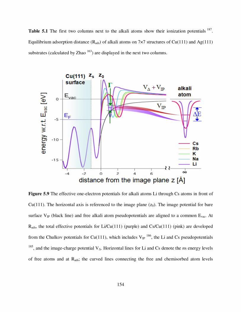
154
Table 5.1 The first two columns next to the alkali atoms show their ionization potentials 187.
Equilibrium adsorption distance (Rads) of alkali atoms on 7×7 structures of Cu(111) and Ag(111)
substrates (calculated by Zhao 163) are displayed in the next two columns.
Figure 5.9 The effective one-electron potentials for alkali atoms Li through Cs atoms in front of
Cu(111). The horizontal axis is referenced to the image plane (z0). The image potential for bare
surface VIP (black line) and free alkali atom pseudopotentials are aligned to a common Evac. At
Rads, the total effective potentials for Li/Cu(111) (purple) and Cs/Cu(111) (pink) are developed
from the Chulkov potentials for Cu(111), which includes VIP 186, the Li and Cs pseudopotentials
185, and the image-charge potential V∆. Horizontal lines for Li and Cs denote the ns energy levels
of free atoms and at Rads; the curved lines connecting the free and chemisorbed atom levels

155
signify the destabilization and broadening (Γ) of the ns states into surface resonances, as alkali
atoms are brought to the surface.
The chemisorption process alters the electronic structures of the free adsorbate (atoms or
molecules) via chemical and image-charge interactions, as well as interadsorbate interactions at
higher coverages. The image-charge interaction, which is dominant for alkali atoms interacting
with metal surfaces 21,38,188,189,190, arises from the many-body screening of an external charge by
the conduction band electrons in metal. The screening response to an external charge can be
described through the Coulomb field of its fictitious ‘image’ charge, which has the opposite sign
and is located at the position of the mirror image with respect to the image plane. According to
the Chulkov potential, which is employed to simulate the surface structure and the projected
band gap of Cu(111) and Ag(111) surfaces, the image-planes are at 2.07 and 2.20 a0 above the
topmost surface layer, respectively 186. As it is depicted in Fig. 5.1, when an ns valence electron
of an alkali atom is brought to the adsorption distance with respect to the metal surface, it
experiences an attractive Coulomb potential due to its own image given by
, [5.2]
and a repulsive potential due to the negatively charged image of the alkali atom ionic core
, [5.3]
where ‘z’ denotes the distance in the direction normal to the surface and stands for the
electron distance parallel to the surface from the adsorbate’s center.
4z1
VIP −=
( )( ) 2122ads∆ ρzRV
−
++=r
ρr

156
According to chemisorption model proposed by Gurney, transporting a free alkali atom to the
adsorption distance Rads elevates the energy of its ns valence electron through the Coulomb
interaction with the conduction electrons of the substrate rendering it an unoccupied resonance in
the electronic DOS 21. Because the experimental linewidths of the ns resonances are sharp (less
than 0.2 eV) and their energies relative to EF are high (about 3 eV), according to this model, at
low coverage chemisorbed alkali atoms should be fully ionized. As it is illustrated in Fig. 5.9, the
image-charge interaction raises the ns valence electron energy with respect to the free atom
energy by
, [5.4]
where the approximate averaged potentials and assuming the
ns orbital to be centered on ionic core ( , ). Figs. 5.6, 5.7, and 5.8 demonstrate that
the quasistationary states corresponding to the ns valence electron localized on the alkali
adsorbate is independent of ionization potential (I) and chemisorption distance (Rads). The
resonance energy, however, depends weakly on the species of the noble metal substrate;
specifically the binding energies with respect to Evac are on average 1.84 eV and 1.99 eV for
alkali/Ag(111) and alkali/Cu(111) systems, respectively. We note that semi-empirical potentials
similar to those presented in Fig. 5.9 have been used for a long time to address the scattering of
alkali atoms or ions by metallic surfaces 190. In that case, however, the potential and
consequently the ns electron binding energy will evolve during the scattering trajectory
according to the z-dependence of the Coulomb interaction outlined earlier.
In order to rationalize the period-independent binding energy of 0m = states of alkali/noble
metal chemisorption systems, we computed the energies of the alkali-localized quasistationary
ads∆IP 4R1VV∆E +≈+=
ads∆ R21V +≈ adsIP 4R1V −≈
adsRz = 0ρ =r
157
states for a range of heights on Cu(111) and Ag(111) surfaces 163. The time-dependent
Schrödinger equation was solved 188,191 for an electron evolving under the influence of the
effective potential constructed by adding the core-image repulsion V∆ to the semi-empirical
potentials of the free alkali atoms and the substrate (depicted in Fig. 5.10) 185,186. To account for
the change in the surface potential through the increase of the alkali atom coverages, which
stabilizes the 0m = state, the contribution from the surface dipole was also included in the
effective potential by the term
. [5.5]
This potential can also be expressed in terms of ∆Φ by 163
. [5.6]
In order to compare with the experimental findings, the computed 0m = state energies given in
Fig. 5.10(a), which are obtained by solving the Schrödinger equation for the effective one
electron potential, have to be taken at the correct adsorption heights Rads. Because the empirical
values of Rads are available for a few chemisorption pairs, typically at 1 ML coverage 20, we
computed the optimized structures including Rads in the low energy coverage limit (see Table
5.1) by plane wave pseudopotential DFT computations for Li through Cs on Cu(111) and
Ag(111) substrates 163,192.
To compare with the experimental measurements in Fig. 5.8(a), the calculated coverage
dependent 0m = binding energies for Li through Cs on Cu(111) and Ag(111) surfaces are
presented in Fig. 5.8(b). Despite the significant differences between the ns electron binding
energies of the free alkali metal atoms, in good agreement with the experimental trends, our
( ) ads23
µ µRπσ2∆E −=
( ) ( ) ads2123
µ R2µ∆Φ∆E −−=

158
theoretical model predicts the common 0m = binding energies of -2.17 and -2.05 eV for the
chemisorbed Li through Cs, respectively, on Cu(111) and Ag(111) surfaces.
Based on the successful simulation of the electronic structure of chemisorbed alkali atoms with
effective potentials, one can understand the period-independent nature of the 0m = binding
energies by simple arguments. Recalling that the ns valence electron localized around the alkali
ion feels the repulsion ∆E owing to the image-charge interaction, its common binding energy
(EB) can be approximated by
. [5.7]
This common binding energy evidently requires the period-dependent ionization potential (I) to
be compensated by the net Coulomb repulsion (∆E), which is inversely proportional to the
adsorption distance, Rads. Therefore, it suggests that there is an anticorrelation between I and Rads,
which can be clearly seen in Fig. 5.10(b) where ‘I’ is plotted against the calculated values of
‘Rads’ for Li through Cs on Cu(111) and Ag(111) surfaces. This anticorrelation is a consequence
of screening of the Coulomb potential of the alkali atom nucleus by its core electrons. Both the
Coulomb potential and the Pauli exclusion determine how the ionic alkali core interacts with its
ns valence electron and the conduction electrons of the substrate. The binding energy ‘–I’ of free
alkali atom ns valence electron is related to its chemisorption distance ‘Rads’ via the same
Coulomb interaction and Pauli exclusion.
I4R
1I∆EE
adsB −
=−=

159
Figure 5.10 Computed results for the alkali/noble metal chemisorption 163: (a) The energies of
0m = states versus the chemisorption height (Rads is given in terms of both atomic units a0
(lower axis) and Å (upper axis)) for Li through Cs on Cu(111). The horizontal line at -2.17 eV is
the computed average alkali atom 0m = binding energy taken at the Rads from DFT calculations
(marked by the intersecting vertical lines). (b) The anticorrelation between Rads for Li through Cs
Cu(111)
Ag(111)
(b)
1.2 1.4 1.6 1.8 2.0
2.0 2.5 3.0 3.5 4.0
(a)
CsRbKNaLi
(c)
-1.5
-2.0
-2.5
-3.0
-5.0
-4.5
-4.0
3.0
2.0-2.0
-4.0
-5.0
bin
din
g
ener
gy
[eV
]io
niz
atio
n
po
ten
tial
[eV
]b
ind
ing
en
erg
y [e
V]
chemisorption height [Å]
chemisorption height [a0]

160
(left to right) and the free atom ionization potentials ‘I’ for Cu(111) and Ag(111). (c) The
electron binding energy of the free alkali ions (-I; blue squares) and the total level shift ∆E
( ; green triangles) together define the 0m = binding energy EB
( ; red dots) for Li through Cs on Cu(111).
The computed values of the repulsive (∆E) and attractive (–I) interactions and the resulting
binding energy ( ) of the ns valence electrons at Rads on Cu(111) surface are depicted
in Fig. 5.10(c). The electron binding energy of the free alkali atoms (–I; blue squares) and the
image-charge repulsion (∆E; green triangles) increase in magnitude with the opposite sign with
decreasing size of alkali ionic core, and therefore Rads. These periodic trends are mostly balanced
in their sum EB (red dots), which is nearly period-independent, and corresponds to an average
0m = binding energy of -2.26 eV in agreement with the more elaborate wave packet
propagation calculations (by Zhao 163).
The experimental results and the successful theoretical models developed for the alkali atom–
noble metal interactions in predicting the unoccupied electronic structure of the chemisorption
interface corroborates the original proposals of Langmuir and Gurney that the interaction is
largely of ionic character 13,21. This standpoint does not disqualify that covalent interactions may
play a minor yet increasingly significant role for smaller alkali atoms and for transition metal
surfaces 34,174.
Our model, which was implemented by Zhao 163, accounts for only the Coulomb interaction and
the Pauli exclusion experienced by the outermost (ns valence) electron of the free and
ads∆IP 4R1VV +≈+=
I∆E −=
I∆EEB −=

161
chemisorbed alkali atoms. It excludes the covalent interactions where bonding electrons occupy
orbitals shared between the adsorbate and the substrate. It agrees well with our experimental
findings, and explains the period-independent electronic structure of the alkali atom/noble metal
chemisorptions interface. Therefore, with the free atom or molecule electron binding energy and
the adsorption distance Rads only, one can predict the energy of the quasistationary state at the
adsorbate–metal interface with a well-defined charge configuration in both the highest occupied
and the lowest unoccupied molecular orbitals (HOMO and LUMO, respectively).
The results presented here substantiate the fundamental role of Coulombic image charge
interaction in determining the position of the HOMO and the LUMO of a wide range of
molecules chemisorbed on metal surfaces. Though the role of the interfacial dipole potential is
generally included in the discussion of orbital energy shifts upon chemisorption, the important
VIP contribution is often omitted 163. The HOMO, and the ionization level in general, of
adsorbates is raised by owing to the interaction with the image charge. This effect
compensates the change in the atomic ionization potential (I) for alkali atoms nearly exactly and
gives rise to a period-independent binding energy of 0m = . Also, the LUMO, or affinity level, is
stabilized by the electronic image potential by . This results in an energy difference
between HOMO and LUMO equal to . Our model for the electronic structure of alkali
atom chemisorption is capable of reproducing these shifts as long as the electronic states are
localized on the adsorbates; its extension and applications to a wide range of molecule/metal
interfaces with definite electronic properties appear to be possible 163.
ads4R1∆E =
ads4R1−
ads2R1
162
5.2 Discovery of the 1m = Alkali-Induced Resonance by Angle-Resolved Two-Photon
Photoemission
5.2.1 Introduction
In the previous section, we described the experimental and theoretical analysis of the lowest
0m = resonance of alkali atoms on noble metals that was already predicted to exist by Gurney.
Although alkali atoms have rich electronic spectra in the gas phase, so far nothing has been
known experimentally or theoretically about higher lying electronic states above the 0m =
resonance, even though the existence of such resonances has been predicted by calculations of
Nordlander and Tully at large atom-surface distances 38. The first study of the higher lying
electronic states at the chemisorption distance was the prediction of an (or π) resonance
0.5 eV above the m = 0 resonance for Cs/Cu(100) using the same theoretical methods as
introduced in the previous section 193 . Such higher lying states could provide additional
information on the alkali atom–noble metal interaction that could have broad implications to
other adsorbates.
In this section, we describe the experimental discovery of this π-resonance by AR2PP. This new
state is observed at eV above the states, confirming the theoretical predictions
51,193. Comparison between the experiment and theory shows that these newly found states are
formed by the admixture of alkali atom np and (n-1)d valence orbitals of the π-symmetry, i.e.,
they are antisymmetric with respect to the surface normal 163.
1m ±=
7.03.0 − 0m =

163
5.2.2 Angle-Resolved Two-Photon Photoemission Measurements
We investigated the symmetry states for Cs and K on Cu(111) and Cs, K, and Na on
Ag(111). The experiments were carried out as in the previous section, except that we also
measured the angle-resolved spectra using the same procedure as described in Chapter-4.2 for
the bare Ag(111) surface.
Figs. 5.11 and 5.12 present the AR2PP spectra for Cu(111) and Ag(111) surfaces. The images on
the left side (5.11(a), 5.11(c), 5.12(a), 5.12(c), and 5.12(e)) are the 2PP spectra presented as
contour plots of 2PP intensity as a function of the emission angle and the intermediate state
energy. The waterfall images on the right side (5.11(b), 5.11(d), 5.12(b), 5.12(d), and 5.12(f)) are
the same angle-dependent 2PP spectra that have been displayed on a parallel momentum (k||)
scale using the conversion given by equation [3.1]. Thus, the waterfall images show the 2PP
intensity as a function of the parallel momentum and intermediate state energy. Although the
original data are the same, the sinθ dependence in equation [3.1] causes the conversion from
angle to momentum to be nonlinear.
1m ±=

164
Figure 5.11 The AR2PP spectra of K/Cu(111) surface presented as contour plot (a) of 2PP
intensity as a function of the emission angle and intermediate state energy. 3.1 eV corresponds to
excitation from the Fermi edge. In (b) the same data are plotted as a waterfall image of 2PP
intensity against the parallel momentum and intermediate state energy. The AR2PP spectra of
Cs/Cu(111) surface are also presented as a contour plot (c) and the waterfall image (d). The
spectroscopic features corresponding to the resonant interband ( ) excitation (orange
dashed lines), the Shockley surface state (SS; red dashed lines), the alkali localized (σ;
blue dashed lines) state and the (π; black dashed lines) intermediate states are indicated.
(a) (b)
(c) (d)
-20
-10
0
10
20
emis
sion
ang
le [d
eg]
3.02.52.01.5intermediate state energy [eV]
20151050
x103
20x103
10
0
phot
oem
issi
on [c
ps]
3.02.52.01.5intermediate state energy [eV]
-0.4
0.0
0.4
Usp ← Lsp
m=0 SS
m=1
20x103
10
0phot
oem
issi
on [c
ps]
3.02.52.01.5intermediate state energy [eV]
-0.4
0.0
0.4
k|| [1/Å]-20
-10
0
10
20
emis
sion
ang
le [d
eg]
3.02.52.01.5intermediate state energy [eV]
20100
x103
k|| [1/Å]
K/Cu(111)
Cs/Cu(111)
(a) (b)
(c) (d)
spsp LU ←
0m =
1m ±=

165
Figure 5.12 (a) The AR2PP spectra of Na/Ag(111) surface presented as contour plot of 2PP
intensity as a function of the emission angle and intermediate state energy. (b) The same data are
-20
-10
0
10
20
emis
sion
ang
le [d
eg]
3.02.52.01.5intermediate state energy [eV]
1050
x103
15x103
10
5
0
phot
oem
issi
on in
tens
ity [c
ps]
3.02.52.01.5intermediate state energy [eV]
-0.4
0.0
0.4
k|| [1/Å]
-20
-10
0
10
20
emis
sion
ang
le [d
eg]
3.02.52.01.5intermediate state energy [eV]
806040200x103
100x103
50
0phot
oem
issi
on in
tens
ity [c
ps]
3.02.52.01.5intermediate state energy [eV]
-0.4
0.0
0.4
k|| [1/Å]
Na/Ag(111)
K/Ag(111)
Cs/Ag(111)
(a) (b)Usp ← Lsp
m=0
SS
m=1(c)
(d)
(e)(f)
20
10
0
-10
-20
emis
sion
ang
le [d
eg]
3.02.52.01.5intermediate state energy [eV]
40200
x103
60x103
40
20
0phot
oem
issi
on in
tens
ity [c
ps]
3.02.52.01.5intermediate state energy [eV]
-0.4
0.0
0.4
k|| [1/Å]
166
plotted as a waterfall image of 2PP intensity against the parallel momentum and intermediate
state energy. The contour plots (c) and (e) and the waterfall images (d) and (f) of AR2PP spectra
of K/Ag(111) and Cs/Ag(111), respectively, are also presented. The spectroscopic features
corresponding to the resonant interband ( ) excitation, the Shockley surface state (SS),
the alkali localized (σ) state and the (π) intermediate states are indicated as in Fig.
5.11. The π-resonance is not observed for Na/Ag(111) surface.
Figure 5.13 shows the energy level structure for K adsorbed Cu(111) and Ag(111) surfaces, the
k||-dispersion of the of the substrate bands, and 2PP excitation pathways that explain some of the
features in AR2PP spectra in Figs. 5.11 and 5.12. Intensity of the 2PP spectra at finite alkali
coverage have contributions from photoexcitation from the Shockley surface state and lower sp-
band of the substrate. The 2PP signal can be resonant with the adsorbate resonances, or occur
through virtual intermediate states, as discussed in Chapter 4.1. For reasons that are unknown,
the lower sp-band features in Cu(111) are much less prominent than for Ag(111). The alkali
atom resonances, which do not disperse with k||, can act as intermediate states in 2PP process as
long as energy conservation is satisfied.
spsp LU ←
0m = 1m ±=

167
Figure 5.13 Two-photon photoexcitation pathways (red arrows) for (a) K/Cu(111), (b)
K/Ag(111) surfaces and the corresponding energy diagrams of the states with respect to parallel
momentum (k||). The clean surface (dashed) and shifted (solid) Evac (orange) and SS (green)
energies are indicated. The 0m = and 1m ±= resonance energies correspond to the observed
values in Figs. 5.11 and 5.12.
For all of the chemisorption pairs studied here, except for the Na/Ag(111) surface, in addition to
the 0m = resonance, alkali atom adsorption induces another feature at higher energy, which has
minimum intensity for normal emission and peaks for emission angles of approximately
°±°± 217 . Based on the calculations of Borisov et al. 51,193 using the same model potentials as in
section 5.1, as well as the symmetry implied by AR2PP spectra, we assign these new resonances
for K and Cs adsorbed on Cu(111) and Ag(111) surfaces to states with 1m ±= , or π-symmetry
6
5
4
3
2
1
0
-1
ener
gy [e
V]
-0.5 0.0 0.5k|| [1/Å]
6
5
4
3
2
1
0
-1
ener
gy [e
V]
-0.5 0.0 0.5k|| [1/Å]
Usp
Lsp
Evac
SS
EF
Emax(a) K/Cu(111) (b) K/Ag(111)
m=0
m=1
m=0
m=1

168
168. These new states appear about eV above the 0m = resonance. These newly
discovered resonances have to correspond to 0|m| > symmetry, i.e., states described by wave
functions with a nodal plane in the surface normal direction.
Whereas the resonance, which corresponds to the ns and npz hybridized orbitals, is
symmetric with respect to the normal emission angle, the resonance, which corresponds
to the hybridization of npx and npy with the (n-1)d orbitals, is the lowest energy antisymmetric
state. Specifically, the npx and npy orbitals, which lie in the plane parallel to the surface, give rise
to two degenerate π-resonances 168. As Figs. 5.11(a) and 5.11(c) demonstrate, the AR2PP
intensity of the resonance on alkali adsorbed Cu(111) surface manifests a minimum for
the emission normal to the surface and distinct maxima at emission angles of °±°± 217 . Similar
angle-dependent behavior is observed for K and Cs on Ag(111) (Figs. 5.12(c) and 5.12(e));
however, the angular photoemission maxima are obscured by spectral overlap with the more
intense two-photon transition. At the angle where the dispersive and nondispersive
states overlap, the resonance serves as a resonant intermediate state in the 2PP process;
and therefore, its angle-dependent intensity reflects the resonance condition in addition to the
wave function symmetry. For both substrates, the photoemission intensity with respect to the
surface normal is not symmetric, because rotating the sample alters the Fresnel factors, as
discussed in Chapter-4.2 147. As a representative example of all of the surfaces discussed here,
we give the calculated photoemission angular distribution for the 1m ±= resonance of
Cs/Cu(111) case for (Fig. 5.14) based on the wave functions from our calculations. The
calculated angular distribution has a minimum for normal emission and a peak at 21° from the
surface normal, in agreement with the experimental data 168.
7.03.0 −
0m =
1m ±=
1m ±=
spsp LU ←
1m ±=
1m ±=

169
Figure 5.14 Calculated angular distribution of photoelectrons from the quasistationary
resonance on Cs/Cu(111) by Borisov. The calculated photoemission angular distribution from
from the npx and npy orbitals of Cs atom parallel to Cu(111) surface exhibits a maximum at
from the surface normal 168.
All of the alkali-localized resonances undergo energy downshift toward EF at finite alkali
coverage as discussed for the 0m = resonance in section 5.1 45,49,51,163. Within the range of alkali
atom coverage permitted by the work function decrease in our experiments, which is more or less
1.5 eV, the stabilization by the surface dipole fields of K and Cs allows observation of both the
0m = and 1m ±= resonances. Unlike the K and Cs cases, the Na/Ag(111) surface does not
reveal any feature of 1m ±= symmetry, most likely because its energy is more than 0.7 eV
above the state, and thus, it cannot be excited in our experiments. The reason why the
1m ±= resonance may be at a higher energy for Na, than for K and Cs, is because for Na the
1)d( −n orbitals are not available to hybridize with the 3px and 3py orbitals.
0 20 40 60 80emission angle θ [deg]
px or py θ
e-
vacuum
solid
phot
oem
issi
on in
tens
ity [c
ps]
1m ±=
o21θ =
0m =

170
Calculations by Borisov et al. 168 predict the location of the state to be about
eV above the state. Thus, the predicted energy splitting is larger than the experimentally
observed values of eV. This can be partially ascribed to the finite adsorbate coverage
used in our experiments. The and symmetry states undergo different energy
shifts due to the potential of the adsorbate dipole layer. In addition to the simple ‘electrostatic
potential’, one also has to take into account the interaction between π-orbitals situated at
neighboring adsorbates, which can be larger for npx and npy orbitals than for the ns and npz
orbitals 168.
In summary, for alkali atoms on Cu(111) and Ag(111) surfaces we report the discovery of a
theoretically predicted π-symmetry ( ) resonance, in addition to the well-known σ-
symmetry ( ) resonance. These results should be of general nature for metal substrates
having a projected energy band gap and adsorbate atoms, which chemisorb mainly in an ionic
state. Our experimental observation of an antisymmetric state with respect to the surface normal,
which responds to the external electromagnetic fields and resonant states of the substrate with
different symmetry selection rules than the well-known state, opens up new possibilities
to study how electronic symmetry influences the adsorbate electronic structure and interactions
with the substrate 168. The discovery of the states also provides primary information on
the influence of atomic orbital symmetry on the angle-dependent photoelectron distribution from
a surface that was predicted more than 30 years ago by Gadzuk 194, and exploited in studies of
the structure and dynamics of gas phase molecules 195. Although photoemission spectroscopy has
been used for band mapping in solids and wave function imaging in the gas phase 196,197, the
1m ±= 1.18.0 −
0m =
7.03.0 −
0m = 1m ±=
1m ±=
0m =
0m =
1m ±=
171
imaging of the wave function angular distributions of chemisorption systems remains a largely
uncharted territory. Our work may stimulate fruitful studies in this field.
5.3 Conclusion to Alkali Atom Chemisorption on Noble Metals
Stimulated by theoretical calculations of Borisov et al., we have carried out 2PP and AR2PP
experiments on the electronic structure of alkali atoms on noble metal surfaces 163,168. The model
for the interaction of alkali atoms with noble metals successfully describes the unoccupied
electronic structure of the chemisorption interface, which was originally proposed by Langmuir
and Gurney 13,21. Our systematic and comprehensive measurements reveal interesting periodic
insensitivity of the interfacial electronic structure that allows us to develop a simple and nearly
quantitative model for the alignment of the adsorbate-induced resonances. The discovery of a
higher lying π-symmetry state on the same chemisorption systems at nearly the expected energy
as observed in our experiments substantiates the theoretical model 51,193. Our experimental
investigations coupled with theory enabled us to acquire significant insight into one of the
simplest chemisorption interfaces that could be extended to developing a general understanding
of the band alignment at metal-molecule interfaces.

172
Chapter-6
Surface Femtochemistry: Observation of Frustrated Alkali Atom
Desorption
Observation of transient intermediate states of a surface chemical reaction is one of the most
fundamental problems in surface science 55,198 . The femtochemistry for gas phase chemical
reactions have been pioneered by Zewail and coworkers 199 . With femtosecond laser based
pump–probe spectroscopic methods, it is now possible to follow the outcome of light-induced
chemical reactions in the gas and solution phase on the time scale of the nuclear vibrational
motion.
Observing the process of photoinduced chemical reactions on solid surfaces is also of
considerable fundamental and technological interest; electronic excitation of surface adsorbates
gives rise to considerably different reaction products and product energy distributions than
results from conventional thermal activation 56. A particularly powerful way to follow
photoexcitation-induced nuclear dynamics on solid surfaces is by TR2PP 54,55,56. In surface
femtochemistry, ultrafast laser pulses excite adsorbates to dissociative potential energy surfaces
and follow the nuclear motion through the evolution of the surface electronic structure. This can

173
be accomplished with two ultrafast optical pulses to start the desorption process, and after a
variable time delay, interrogate the transition state through changes in 2PP spectra during the
course of a chemical reaction 51,200. In addition to the electronic response to the nuclear motion,
TR2PP also probes the decay of the excited state population through the elastic resonant charge
transfer (RCT) from the adsorbate to the conduction band continuum of the substrate, as well as
the inelastic electron-electron scattering with electrons in the Fermi sea 201,202. The excited state
wave packet motion can also change the 2PP process, as we will argue in the case of Cs/Ag(111).
So far, surface femtochemistry techniques have been applied to the frustrated desorption of Cs
from Cu(111) surface 54,55,56, 203 and electron solvation in protic solvents on metal 204 and
semiconductor 205 surfaces.
6.1 Why Ultrafast Techniques?
The outcome of a surface photochemical reaction can be studied either by postmortem methods
that detect the desorbed reaction products in the gas phase, or directly on surface during the
course of chemical transformation. Because the ultrafast electronic relaxation of adsorbates
quenches the dominant dynamical processes before the reaction products can desorb, it is
difficult and questionable to extrapolate from the exceedingly small quantum yields and energy
distributions of the gas phase products back to the dynamics that led to the observed outcome.
The development of femtosecond lasers with pulse durations shorter than the typical period of
molecular vibration has made it possible to observe chemical reactions directly on surface in
terms of coherent nuclear wave packet motion and even to devise optical fields that can change

174
their course of evolution, provided that the electronic relaxation does not quench the nuclear
motion 56,203,206.
The lifetimes of electronic excitations and their decay pathways on solid surfaces are poorly
known. A pessimistic picture emerges from estimates of sub to few femtosecond time scale 207,208
excited state lifetimes based on the analysis of spectroscopic linewidths of the unoccupied states.
The main relaxation pathway is RCT from the adsorbate-localized states to the propagating states
of the substrate conduction band continuum. Direct TR2PP measurements, however, often show
that either or both the ultrafast dephasing and inhomogeneous broadening dominate the
linewidths, while the actual excited state lifetimes are considerably longer 180.
Photodesorption is one of the most fundamental surface photochemical processes. Alkali atoms
on noble metal surfaces are particularly well-suited for such studies because of their strongly
bound ionic ground states, and dissociative neutral exited states. Their simple electronic
structures and relatively long excited state lifetimes ( 5010− fs) have attracted several
experimental and theoretical investigations of the photodesorption dynamics 54, 209 . The
Cs/Cu(111) chemisorption system has been of particular interest, because the relatively long
(~50 fs) lifetime of its 0m = resonance facilitates the observation of its nuclear wave packet
motion despite the large mass of Cs atoms 54. The photoinduced charge transfer excitation
prepares the excited state consisting of a neutral Cs atom at the equilibrium position of the ionic
ground state, triggering repulsive forces that initiate the dissociative wave packet motion.
Interferometric time-resolved two-photon photoemission (ITR2PP) measurements reveal the
nuclear wave packet motion during the initial phase of the photodesorption process, which is

175
eventually terminated by the nonadiabatic transition to the ground state potential through RCT of
6s electron back to the substrate 56. This frustrated photodesorption of alkali atoms has been the
subject of several theoretical publications, which aim to describe the excitation, deexcitation, and
wave packet propagation dynamics 210 , 211 , 212 , 213 . Questions remain as to whether similar
photodesorption dynamics could be observed for other alkali/noble metal systems. Theoretical
calculations for alkali atoms on Cu(111) and Ag(111) surfaces predict the Cs/Cu(111) system to
be unique in decoupling the 0m = resonance from the various elastic and inelastic decay
channels 28,173,214. Previous measurements for both surfaces seem to concur 55,214; in this Chapter,
however, we show this pessimistic conclusion to be unfounded.
Photoexcitation in a surface photochemical reaction could proceed, as shown in Fig. 6.1, either
directly by the optical excitation of an unoccupied state of adsorbate from the occupied states of
the adsorbate or the substrate, or indirectly by the scattering of photogenerated hot electrons
from the substrate to the adsorbate 55. Most literature on surface photochemistry invokes the
indirect, hot electron mechanism 215,216,217,218, whereas 2PP spectroscopic studies nearly always
find the direct charge transfer excitation from the substrate to be dominant 55,105. The resonance
behavior, for example, for the SS0m ←= excitation for Li through Cs on Cu(111) in Fig.
5.6(a), shows that the direct mechanism dominates for alkali atoms on noble metals.
The electronic quenching of an excited state, which is largely responsible for the low efficiency
of surface photochemical reactions, can occur either through RCT or electron-electron scattering.
Although it is difficult to distinguish experimentally, theoretical calculations predict that for
alkali atoms either electronic quenching mechanism can dominate depending on the properties of
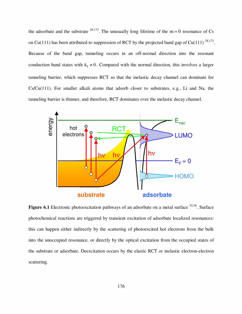
176
the adsorbate and the substrate 28,173. The unusually long lifetime of the 0m = resonance of Cs
on Cu(111) has been attributed to suppression of RCT by the projected band gap of Cu(111) 28,173.
Because of the band gap, tunneling occurs in an off-normal direction into the resonant
conduction band states with 0k || ≠ . Compared with the normal direction, this involves a larger
tunneling barrier, which suppresses RCT so that the inelastic decay channel can dominate for
Cs/Cu(111). For smaller alkali atoms that adsorb closer to substrates, e.g., Li and Na, the
tunneling barrier is thinner, and therefore, RCT dominates over the inelastic decay channel.
Figure 6.1 Electronic photoexcitation pathways of an adsorbate on a metal surface 55,56. Surface
photochemical reactions are triggered by transient excitation of adsorbate localized resonances:
this can happen either indirectly by the scattering of photoexcited hot electrons from the bulk
into the unoccupied resonance, or directly by the optical excitation from the occupied states of
the substrate or adsorbate. Deexcitation occurs by the elastic RCT or inelastic electron-electron
scattering.
RCTLUMO
HOMO
EF = 0
Evac
substrate adsorbate
hot electrons
hν hν hν
ener
gy

177
6.2 Experiments
We have performed I2PC measurements for alkali atoms (Li, Na, K, and Cs) on Ag(111) and
Cu(111) surfaces. As predicted by theory 28, the electronic relaxation of 0m = resonances of Li
and Na was too fast to observe the nuclear wave packet motion. Therefore, we focused on K and
Cs on Ag(111), for which we performed I2PC measurements as a function of electron energy and
emission angle. The angle-resolved measurements were in part motivated by interest in the
dynamics of the newly discovered 1m ±= resonance that is described in Chapter-5.2. For that
reason, we also performed angle-resolved I2PC measurements for K and Cs on Cu(111). Also,
for Cs on multilayer Ag(111) films, Aeschlimann and coworkers reported angle-dependent
intermediate state lifetimes, which they attributed to a contribution to the signal from the bulk
intermediate states 53. Because bulk states do not exist at the energy and k|| of their measurements,
the origin of k||-dependent lifetimes must be reexamined.
Most of the experimental procedures for the angle-resolved I2PC measurements were similar to
those used in Chapter-4.2 and 5.2. In order to ensure that sufficient alkali atom coverage had
been achieved to observe the 1m ±= resonance, K and Cs were deposited from their getter
sources with the sample rotated by about 20° from the analyzer axis, while continuously
recording 2PP spectra. I2PC scans were recorded at fixed energy increments of 0.1 eV over the
energy range extending from the spsp LU ← transition ( 1.8~Eint eV) to the Fermi edge. With
simultaneous acquisition for 7 different energies, this energy region could be covered with two
data acquisition cycles for each angle. Each acquisition cycle corresponded to averaging of
800600− pump-probe scans to obtain better statistics. The measurements in each acquisition

178
overlapped at one energy to check for the consistency between the runs; therefore, data were
obtained for 13 distinct observation energies. Moreover, to study the angular dependence of
time-resolved measurements, I2PC scans were recorded at various photoemission angles from 00
through 220 in 2-degree increments. The angle was varied by rotating the sample manipulator
manually between the measurements.
6.3 Photoinduced Desorption
Surface femtochemistry occurs by excitation of adsorbates to excited states with potential energy
surfaces that drive nuclear motion from reactants into products. Fig. 6.2 shows the potential
surfaces that represent the critical features for the photodesorption of Cs from Ag(111). Before
excitation, a chemisorbed Cs+ ion exists in the deeply bound well (~2 eV) in its electronic ground
state at the equilibrium distance (Rads). Upon charge transfer excitation of an electron to the
0m = resonance, the ground state probability distribution (green Gaussian curve) is projected
onto the neutral AgCs − surface. Because of the repulsive interaction between the 6s electron
and the image charge of the Cs+ core, upon the vertical excitation onto the neutral excited state,
the Cs atom experiences a strong repulsive force causing the AgCs − bond to rupture 51,54,55,56.
Therefore, the wave packet (blue Gaussian curve) motion takes place according to the ‘repulsive’
Menzel-Gomer-Redhead scheme 219,220. In this scheme, dissociation will occur either on the
excited state surface, or if it is electronically quenched, on the ground state surface. In the latter
case, the desorption can only occur, if the kinetic energy acquired by propagating on the excited
state surface is sufficient to overcome the potential barrier to products on the ground state
surface.

179
Because the 0m = resonance energy decreases as the AgCs − bond is elongated, as implied by
Fig. 5.9, the photoinduced motion of Cs cause the 0m = resonance to appear at a lower energy
in 2PP spectra when probed by a delayed probe pulse 184. This relationship between the 0m =
resonance energy and the bond length can be understood from Fig. 5.10(a). The asymptotic
energy of the Cs+ desorption product is indicated by the blue horizontal line; the origin of the
energy axis corresponds to free Cs atom in vacuum at rest.
Figure 6.2 The potential energy surfaces for photoinduced desorption of Cs from Ag(111)
surface 54,55,56. The origin of the energy scale corresponds to Cs atom at rest in the vacuum; the
blue horizontal line indicates the asymptotic energy of free Cs+ at rest. The pump pulse projects
the ground state wave packet (green Gaussian) onto the excited state, turning on the repulsive
forces between Cs and the substrate. The evolving wave packet (blue Gaussian) can be deduced
Ekin
Ag- + Cs+
Cs+
Ag + Cs
alkali – image plane distance (Rads)
3
2
1
0
-1
-2
pump
probe
nucl
ear
pote
ntia
l ene
rgy
[eV
]
Rads Rc
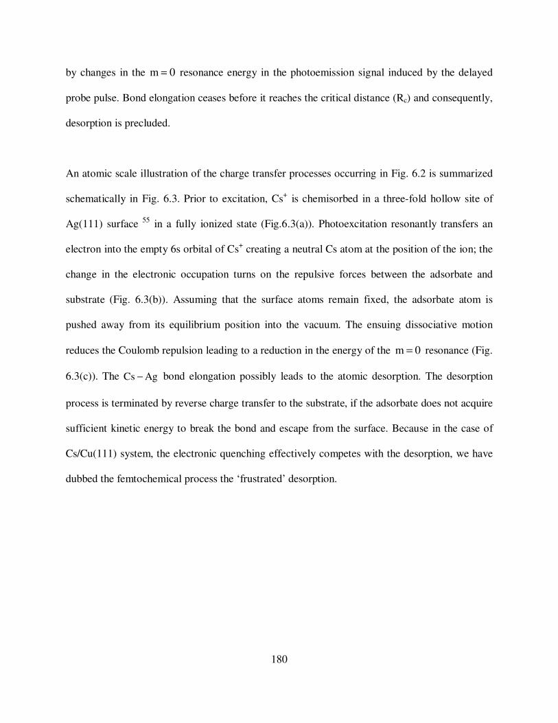
180
by changes in the 0m = resonance energy in the photoemission signal induced by the delayed
probe pulse. Bond elongation ceases before it reaches the critical distance (Rc) and consequently,
desorption is precluded.
An atomic scale illustration of the charge transfer processes occurring in Fig. 6.2 is summarized
schematically in Fig. 6.3. Prior to excitation, Cs+ is chemisorbed in a three-fold hollow site of
Ag(111) surface 55 in a fully ionized state (Fig.6.3(a)). Photoexcitation resonantly transfers an
electron into the empty 6s orbital of Cs+ creating a neutral Cs atom at the position of the ion; the
change in the electronic occupation turns on the repulsive forces between the adsorbate and
substrate (Fig. 6.3(b)). Assuming that the surface atoms remain fixed, the adsorbate atom is
pushed away from its equilibrium position into the vacuum. The ensuing dissociative motion
reduces the Coulomb repulsion leading to a reduction in the energy of the 0m = resonance (Fig.
6.3(c)). The AgCs − bond elongation possibly leads to the atomic desorption. The desorption
process is terminated by reverse charge transfer to the substrate, if the adsorbate does not acquire
sufficient kinetic energy to break the bond and escape from the surface. Because in the case of
Cs/Cu(111) system, the electronic quenching effectively competes with the desorption, we have
dubbed the femtochemical process the ‘frustrated’ desorption.
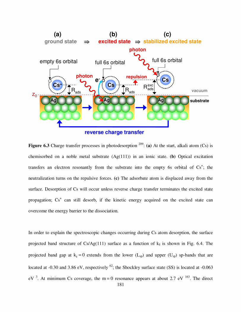
181
Figure 6.3 Charge transfer processes in photodesorption 209: (a) At the start, alkali atom (Cs) is
chemisorbed on a noble metal substrate (Ag(111)) in an ionic state. (b) Optical excitation
transfers an electron resonantly from the substrate into the empty 6s orbital of Cs+; the
neutralization turns on the repulsive forces. (c) The adsorbate atom is displaced away from the
surface. Desorption of Cs will occur unless reverse charge transfer terminates the excited state
propagation; Cs+ can still desorb, if the kinetic energy acquired on the excited state can
overcome the energy barrier to the dissociation.
In order to explain the spectroscopic changes occurring during Cs atom desorption, the surface
projected band structure of Cs/Ag(111) surface as a function of k|| is shown in Fig. 6.4. The
projected band gap at 0k|| = extends from the lower (Lsp) and upper (Usp) sp-bands that are
located at -0.30 and 3.86 eV, respectively 62; the Shockley surface state (SS) is located at -0.063
eV 3. At minimum Cs coverage, the 0m = resonance appears at about 2.7 eV 163. The direct
vacuum
substrate
Cs+
empty 6s orbital full 6s orbital
e-
full 6s orbital
(a) (b) (c)
repulsion
ground state ⇒⇒⇒⇒ excited state ⇒⇒⇒⇒ stabilized excited state
Rads
CsCs
Rads
excadsR
Ag Ag Ag-z0
photon
reverse charge transfer
photon

182
photoexcitation of 0m = resonance occurs by photoinduced charge transfer from the lower sp-
band; because the 0m = resonance is localized on Cs atoms, excitation is possible from any
momentum state that conserves energy. Following the excitation, the decrease in energy of the
0m = resonance with time can be detected after a delay (τ) by completing the 2PP process with
the delayed probe pulse. Monitoring the dynamics at different k|| should probe the same 0m =
resonance, which is localized on Cs atom. The evolution of the 0m = resonance wave function
can change the k|| spectrum that defines the localized state.
Figure 6.4 The surface projected band structure of Cs/Ag(111) along the parallel component of
momentum (k||). Energy of the 0m = resonance changes with the pump-probe delay due to the
dissociative wave packet motion. (τ: pump-probe delay time)
6
5
4
3
2
1
0
-1
ener
gy [e
V]
-0.5 0.0 0.5parallel momentum (k||) [1/Å]
Cs/Ag(111)
EF
Evac
Evacred
Φ
Φred
SS
Lsp
Usp
hν
hν
τ=0
τ=100 fs
∆τ
m=0m=0
∆Φ
Emax
Ef

183
6.4 Interferometric Two-Pulse Correlation Measurements
As discussed in Chapter-2.1, I2PC scans measure the phase and energy dynamics of the coupled
states in a 2PP process. In conventional photoemission spectroscopy, the linewidth is often
interpreted as a measure of the hole lifetime 221. In fact, the homogeneous linewidth is a measure
of the electron-hole pair dephasing time. Under some circumstances the contribution of electron
can be neglected so that the linewidth gives a good measure of the hole dephasing 222. Likewise,
linewidths in 2PP spectra provide information on the electron-hole pair dephasing.
The experimental 0m = resonance linewidths for alkali atoms on Ag(111) surface in 2PP
spectra of Fig. 5.7, which are 3.0≥ eV, are broader than for Cu(111) surface 54,180. The larger
linewidths may include both homogeneous and inhomogeneous contributions. The homogeneous
contributions could be larger on account of faster decay of the 0m = resonance. Aeschlimann
and coworkers have reported a lifetime of 7> fs and later 211± fs for Cs on thick ( ML5> )
films of Ag on Cu substrates. The films consisted of thick Ag(111) islands interspersed with thin
( ML21 − ) Ag film 53,214. These lifetimes agreed with the theoretical calculations by
Echenique’s group. For a single crystal Ag(111) substrate, however, Petek et al. reported
significantly longer lifetime of 30 fs 55. If one takes the single crystal results to be more
representative, then the 0m = resonance lifetime contributes negligibly to the broadening of the
experimental linewidth.
Additional contribution to the homogeneous linewidth could arise from the initial state scattering.
Because the 2PP process excites an electron from the lower sp-band of the bulk Ag, rather than

184
the surface state as in the case of Cu(111), the hole scattering could be more effective for
Ag(111). Hole-hole scattering in the bulk is usually more efficient than at surfaces 125. Moreover,
the hole binding energies for alkali atom excitation are larger for Ag(111) than for Cu(111)
surface, and therefore the lifetimes are expected to be shorter 125.
Furthermore, the 0m = resonance linewidth on Ag(111) surface could also have significant
inhomogeneous contribution. Because light couples a broad range of initial k-states of the lower
sp-band of Ag to the Cs atom localized 0m = resonance, the inhomogeneous broadening for the
excitation could be larger than in the case of excitation from the surface state of Cu(111). As a
consequence of these enhanced homogeneous and inhomogeneous broadening contributions, the
effective dephasing times associated with the 2PP excitation through the 0m = resonance
estimated from our I2PC measurements are too fast ( 6≤ fs) to resolve.
In the case of K and Cs on Ag(111), the population dynamics associated with the 0m = and
1m ±= resonances occur on a significantly longer time scale than the dephasing making it
possible to follow the coupling of electronic and nuclear motion through measurement of I2PC
scans. As already introduced in section 6.3, the photoinduced charge transfer excitation can
trigger the ‘frustrated’ desorption of alkali atoms from noble metal surfaces, if 0m = , and
possibly 1m ±= resonance lifetimes are sufficiently long to allow appreciable nuclear wave
packet motion 54,55,56,180. In the following, we will discuss mainly the I2PC measurements of
0m = dynamics for K and Cs on Ag(111) surfaces. I2PC measurements were also performed for
K and Cs on Cu(111) as a function of emission angle; these data will be discussed as they pertain
to the 1m ±= resonance.

185
I2PC measurements for normal emission have been previously reported for Cs on both Cu(111)
and Ag(111) surfaces 164,180. Previous measurements for Cs/Cu(111) at 33 K have revealed that
the population decay can be monitored on a time scale of roughly 200 fs 54,55,56. Although the
excited state wave packet motion causes the population kinetics to be nonexponential, a lifetime
of ~50 fs was estimated 54,180. In fair agreement with experiment, theoretical calculations predict
a lifetime of ~30 fs with dominant contribution from electron-electron scattering 28. As
mentioned above, the lifetime of ~30 fs reported by Petek et al. for Cs/Ag(111) system at 33 K,
is significantly longer than those reported by Aeschlimann’s and Echenique’s groups 55,214.
Our I2PC measurements on Cs/Ag(111) manifest a profound change in the surface electronic
structure following the charge transfer excitation of the 0m = resonance that had not been
observed before. Fig. 6.5(a) shows a series of ‘0ω’ (phase averaged) envelopes of I2PC scans for
different energies that were measured for normal emission from Cs/Ag(111) surface at room
temperature. The same normalized data are plotted in Fig. 6.5(b) as a contour map of 2PP
intensity with respect to the intermediate state energy and pump–probe time delay. The I2PC
scans consist of a Gaussian autocorrelation function of the laser pulse near zero delay, which is
slightly broadened by finite dephasing of the coupled states, as already discussed. Here, we focus
on the longer time scale population dynamics that is responsible for the dramatic changes in Fig.
6.5.
The population dynamics can be classified into regions above and below the 0m = resonance at
2.43 eV. At and above the 0m = resonance peak, the population decay of the intermediate state

186
follows exponential kinetics. At the 0m = resonance maximum the population decays with a
time constant of 333 ± fs, and it is in good agreement with the published single crystal Ag(111)
surface data 55, but not with the thick Ag(111) film data or theory 214. At the energies below the
0m = resonance, however, the intermediate state population dynamics follow increasingly
nonexponential kinetics, which are most pronounced in the 1.29.1 − eV range.
As in the case of Cs/Cu(111) 54, we interpret the nonexponential population dynamics in terms of
the excited state wave packet propagation. According to Fig. 6.2, the photoexcitation creates a
neutral Cs atom on a repulsive potential surface. The wave packet propagation leads to the
lowering of the 0m = resonance energy as a function of the pump-probe delay. A simplistic, but
incomplete, interpretation of the nonexponential behavior is that the wave packet propagation
causes the rapid energy stabilization of the excited state population as a function of the delay,
and therefore, increasing bond length. According to the contour plot in Fig. 6.5(b), the apparent
0m = state population maximum shifts from ~2.43 eV by ~0.4 eV within a pump–probe delay
of 120 fs. For comparison, within the same time window the experiments on Cs/Cu(111) report
excited state stabilization of only 0.2 eV 54. Because there is a strong dependence of I2PC scans
on the observation angle, next we present the angle-dependent results.

187
Figure 6.5 (a) The measured I2PC ‘0ω’ (phase-averaged) envelopes for different intermediate
state energies. The envelope amplitudes reflect the actual signal strength at each measurement
energy. (b) The 2PP intensity contour plot as a function of the intermediate state energy and
pump-probe delay that has been generated from the I2PC envelopes in (a). The envelopes are
normalized at zero delay.
6.5 Angle-Dependent Interferometric Two-Pulse Correlation Measurements
We measured off-normal I2PC scans to probe the dynamics following the 1m ±= resonance
excitation. Such measurements were performed for K/Ag(111) and Cs/Ag(111). Fig. 6.6 shows
the 0ω envelopes taken for Cs/Ag(111) between 0° and 22º emission angles in 2-degree intervals.
(a) (b)
inte
rmed
iate
sta
te e
nerg
y [e
V]
3.0
2.9
2.8
2.7
2.6
2.5
2.4
2.3
2.2
2.1
2.0
1.9
3.03
2.93
2.83
2.73
2.63
2.53
2.43
2.33
2.23
2.13
2.03
1.93
1.83
inte
rmed
iate
sta
te e
nerg
y [e
V]
min max
-100 0 100pump-probe delay [fs]
-100 0 100pump-probe delay [fs]

188
The scans that coincide with the 0m = and 1m ±= resonances, and the spsp LU ← two-photon
transition are indicated by blue, green and red lines, respectively. We first discuss the unexpected
k||-dependence of the 0m = resonance dynamics.

189
Figure 6.6 I2PC measurements on Cs/Ag(111) as a function of intermediate state energy at
photoemission angles from 0° to 22°. The measurements corresponding to spsp LU ← transition
-150-100-500 -150-100-500 -150-100-500
-150-100-500 -150-100-500 -150-100-500
-150-100-500 -150-100-500 -150-100-500
-150-100-500 -150-100-500 -150-100-500
3.032.932.832.732.632.532.432.332.232.132.031.931.83
3.032.932.832.732.632.532.432.332.232.132.031.931.83
3.032.932.832.732.632.532.432.332.232.132.031.931.83
3.032.932.832.732.632.532.432.332.232.132.031.931.83
inte
rmed
iate
sta
te e
nerg
y [e
V]
pump-probe delay time (τ) [fs]
θ = 0° θ = 2° θ = 4°
θ = 6° θ = 8° θ = 10°
θ = 12° θ = 14° θ = 16°
θ = 18° θ = 20° θ = 22°

190
(red), 0m = (blue), and 1m ±= (green) resonances are indicated by the colored lines. Note that
at °= 20θ the 0m = resonance (blue line) acts as an intermediate state in spsp LU ← two-
photon transition. The 1m ±= resonance is discernible only at large emission angles.
If the I2PC scans were to measure only the population dynamics, and the 0m = resonance were
nondispersive with momentum, then we would not expect to see k||-dependence of I2PC scans. In
fact, the k||-dependence is dramatic. The angle-dependent I2PC envelopes in Fig. 6.6 show clear
differences particularly in terms of the nonexponential dynamics below the 0m = resonance.
The nonexponential behavior is strongest near normal emission, and it becomes unnoticeable to
inspection for °>10θ .
In order to quantify these angle-dependent differences, we developed a simple kinetic model that
can reproduce the nonexponential population dynamics. At and above the 0m = resonance, the
population decay could be modeled as a simple exponential decay convoluted by the coherent
response given mainly by the autocorrelation of the Gaussian laser pulse. Below the 0m =
resonance, in addition to the exponential decay, we included an exponential rise to represent the
rising part of the excited state population signal. We fit the data taken within the 53.283.1 − eV
energy window, since the spsp LU ← transition and the 0m = resonance can be observed within
this interval. The I2PC scans are fitted to
( ) ( ) ( )( ) Bwt
21
expGτtexp1τtexpAtf2
21decay +
−⋅+−−⋅−⋅= , [6.1]
where ‘A’ is the coefficient of the exponentially decaying and rising components with
characteristic times of ‘τ1’ and ‘τ2’, respectively. ‘G’ is the coefficient of the Gaussian function
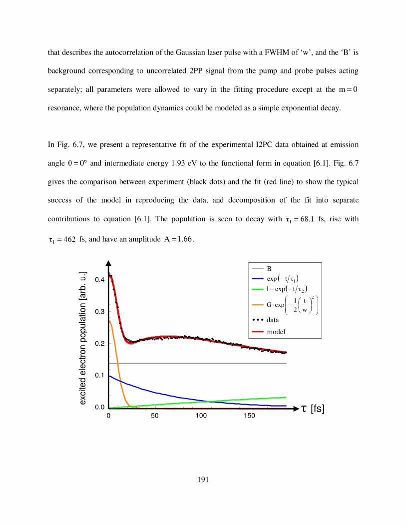
191
that describes the autocorrelation of the Gaussian laser pulse with a FWHM of ‘w’, and the ‘B’ is
background corresponding to uncorrelated 2PP signal from the pump and probe pulses acting
separately; all parameters were allowed to vary in the fitting procedure except at the 0m =
resonance, where the population dynamics could be modeled as a simple exponential decay.
In Fig. 6.7, we present a representative fit of the experimental I2PC data obtained at emission
angle °= 0θ and intermediate energy 1.93 eV to the functional form in equation [6.1]. Fig. 6.7
gives the comparison between experiment (black dots) and the fit (red line) to show the typical
success of the model in reproducing the data, and decomposition of the fit into separate
contributions to equation [6.1]. The population is seen to decay with 68.1τ1 = fs, rise with
462τ1 = fs, and have an amplitude 1.66A = .
50 100 150
0.1
0.2
0.3
0.4
τ [fs]
. ..
B
data
model
( )1τtexp −
( )2τtexp1 −−
−⋅
2
w
t
2
1expG
exci
ted
elec
tron
pop
ulat
ion
[arb
. u.]
0.4
0.3
0.2
0.1
0.00 50 100 150

192
Figure 6.7 Fitting of I2PC data ( °= 0θ emission angle and 1.93 eV intermediate state energy) of
Cs/Ag(111) to our kinetic model expressed in equation [6.1]. The fitted curve is decomposed into
the individual components according the legend.
In Figs. 6.8 and 6.9, we plot the obtained parameters of angle-resolved I2PC scans as a function
of the intermediate state energy and observation angle. The parameters reflect the systematic
changes that can be observed in the experimental scans of Fig. 6.6. In Fig. 6.8, we see that the
amplitude parameter A is sharply peaked at the maximum value of 12.2A = that is obtained for
2.03 eV energy and 0° emission angle. To calibrate the amplitude scale, according to our
normalization procedure, we expect an amplitude of 31A = for resonant excitation. The
significantly larger amplitude at lower energies and angles is not accumulated through the energy
relaxation of the excited state population. The amplitude grows in with a delayed rise far beyond
the population that was generated through the direct excitation.

193
Figure 6.8 The amplitude of ‘A’ of equation [6.1] as a function of the intermediate state energy
and emission angle. The amplitude peaks in the 1.29.1 − eV interval and 0°, where the
nonexponential behavior is the most pronounced.
In Figs. 6.9(a) and 6.9(b), we show the extracted time constants τ1 and τ2 as a function of
intermediate state energy and angle. The decay time τ1 generally increases from ~30 fs at the
0m = resonance resonant excitation energy of 2.43 eV and 0° emission angle. The fluctuations
in the τ1 parameter with energy and angle seem to be real rather than a consequence of deviations
from the model in equation [6.1]. In the case of τ2, the rise time is seen to increase monotonically
to the maximum value of 900 fs at the lowest energy and 0° emission angle.
Figure 6.9 The decay time τ1 (a) and the rise time τ2 (b) of equation [6.1] as a function of the
intermediate state energy and emission angle. In general, the time constants increase for low
energy and small angles. The nonmonotonic changes in τ1 are statistically significant.
intermediate energy [eV]1.9 2.0 2.1 2.2 2.3 2.4 2.5
intermediate energy [eV]1.9 2.0 2.1 2.2 2.3 2.4 2.5
τ1 [fs] τ2 [fs]
0
5
10
15
20
0
5
10
15
20
τ1 τ2
92 0 900 0
(a) (b)

194
The observed dynamics of Cs/Ag(111) are unprecedented and in many respects puzzling. Here,
we provide a heuristic interpretation; the full quantum mechanical modeling required to test the
model is far beyond what has been attempted in previous theoretical models of photodesorption
dynamics, and therefore, will not be attempted here. The main puzzle is the accumulation of
large amplitude at low energies and angles. If we assume that Cs is excited directly, then the
maximum amplitude should occur at the 0m = resonance energy. The total amplitude generated
should be 1/3 at each angle of observation (note again that the I2PC envelopes at different angles
and energies are normalized at 0τ = fs). For the amplitude to rise to 2.12 at its maximum at 2.03
eV and 0° angle, the excited state has to be either generated by another process, or transition
moments for the final excitation step have to depend on the energy and angle of observation.
The intermediate state could be generated by a parallel process such as the hot electron scattering.
This, however, can be immediately excluded because the observed lifetimes for the exponential
rise far exceed the hot electron lifetimes at 2.5 eV above EF 125. The population of 0m =
resonance from the higher lying 1m ±= resonance can also be excluded, because the latter is less
efficiently excited than the former. The other alternative of energy- and angle-dependent
transition moments is more plausible, but it is more difficult to prove. We will return to
discussing it after we consider the time constants in Fig. 6.9.
The decay time τ1 increases from 30 to 92 fs in the energy range of observation. We attribute it in
part to the 0m = resonance decay through RCT and electron-electron scattering. The decay time
becomes longer below the resonance, because, AgCs − bond length increases through the
excited state wave packet propagation. It is natural that the excited state lifetime increases as the

195
coupling of Cs atom to the surface decreases. What is difficult to explain is why the observed τ1
parameter should depend on the angle, because the same Cs atom localized state should be
observed at all angles of observation. Thus, if τ1 only represents the 0m = resonance lifetime,
then it should be independent of the observation angle. It cannot be explained only by angle- and
energy-dependent transition moments invoked earlier. We suspect that the transition moments
decrease for larger angles as the AgCs − bond length increases. The fluctuations in τ1 with angle
and energy could reflect both the variation in the excited state decay as well as the variation in
the transition moments for the intermediate state detection.
The rise time τ2 is probably most closely associated with the wave packet propagation. It requires
time for the AgCs − bond to stretch so that the 0m = resonance appears at a lower energy. We
can estimate the wave packet motion from the dependence of the 6s resonance energy of Cs atom
as a function of distance from the Ag(111) surface, such as we have calculated in Fig. 5.10(a) for
Cs/Cu(111). Based on the nearly linear relationship between the 0m = resonance energy ‘Eσ’
and the bond length ‘R’, we estimate the force exerted on Cs atoms to be 8σ 108.7dR
)R(dEF −×==
N. From Fig. 6.5(b) we see that the amplitude maximum decreases by ~0.39 eV in 100 fs.
Therefore, we ask what is the bond length required to decrease 0m = resonance energy by 0.39
eV, and how long it takes for the AgCs − bond to stretch by the required amount. Based on this
model, the required bond elongation of 0.72 Å is achieved in 190 fs through acceleration with the
constant force. We compare the derived propagation time with the τ2 rise time of 294 fs at 2.03
eV. Although the observed rise time is longer, we note that we have assumed that all the
available momentum is imparted to Cs atom and the surface acts as a massive, rigid wall. This is
196
a better approximation for Ag(111) surface than for Cu(111) surface, because the atomic mass of
the former (107.9 amu) is a better match to Cs atoms (132.9 amu) than the latter (63.5 amu) 223.
We also note that a comparison between classical and quantum mechanical wave packet
propagation for Cs on Cu(111) found the classical model to underestimate the propagation time
by a factor of ~2 212. Thus, we conclude that the τ2 rise time represents mainly the wave packet
propagation.
To conclude the analysis of I2PC scans for Cs/Ag(111) surface, we observe strongly
nonexponential excited state dynamics, which we interpret through the excited state wave packet
motion. As the wave packet propagates, the excited state decays on the time scale given by τ1,
which progressively gets longer as AgCs − bond length increases. At energies below the 0m =
resonance at 0τ = fs, the wave packet appears with a rise time τ2. Even though the rise time
extends to 900 fs at the lowest observed energies, we can detect parts of the wave packet arriving
on ~100 fs time scale. The propagated wave packet rises to its maximum intensity on 100 fs time
scale because of the rapid electronic relaxation on time scale given by τ1. If the transition
moments were constant, the intensity of the propagated wave packet would make it difficult to
observe such long time scale dynamics. In the case of Cs/Ag(111), however, the changing
transition moments seem to selectively amplify the signal so that we can follow the dynamics on
nearly 1 ps temporal and 1 Å length scale. To construct this heuristic scenario, however, we had
to claim that the transition moments for the final step in photoemission depend on the
observation energy and angle. Although we cannot provide a proof, it is easy to rationalize that
this should happen because the 0m = resonance wave functions will evolve as Cs atom desorbs
from the surface. In addition to the change in the Cs atom wave function, the change in the final

197
state energy that is connected by optical transition to the propagating wave packet will also
change during the course of desorption. We leave the modeling of these dynamics as a challenge
to the next generation of students.
In addition to Cs/Ag(111), we also carried out angle-resolved I2PC measurements for K/Ag(111)
in the range of 0° to 20° in 4-degree intervals. The energy- and angle-dependent changes for
K/Ag(111) are much less dramatic than for Cs/Ag(111). The measured population decay time at
the 0m = resonance (~2.5 eV) is 318 ± fs where the average and the variance represent the
scatter between measurements for different angles. The population decay remains exponential
below the 0m = resonance and the lifetimes increase to 556 ± fs while the amplitude of the
population decay component decreases. There are no angle-dependent trends as in Cs/Ag(111).
We attribute these differences with respect to Cs/Ag(111) to the lighter mass (39.1 amu) and
faster RCT decay of neutral K atoms on Ag(111). Being more than three times lighter than Cs, as
well as having shorter Rads, K experiences stronger repulsion and is more effectively accelerated
from the surface than Cs. Therefore, below the 0m = resonance, K atoms appear to be
somewhat stabilized. Because the I2PC measurements do not show strong evidence for the
nonexponential dynamics within the ~200 fs window of our measurements, we conclude that the
extracted exponential decay times are determined mainly by the wave packet decay through the
elastic RCT process.
Furthermore, our angle-resolved I2PC measurements also probe the 1m ±= resonance lifetimes.
Because 1m ±= resonance appears within the wings of the more intense 0m = resonance, it is

198
difficult to attribute the measured decay time constant solely to the 1m ±= resonance lifetime.
The measured I2PC scans at 1m ±= resonance maxima show single exponential kinetics,
therefore, it is not possible to attribute a distinct lifetime to each of the overlapping bands. The
effective 1m ±= resonance lifetimes (in fs) for K and Cs chemisorbed on Ag(111) and Cu(111)
surfaces are experimentally determined and compared with the theoretically predicted values in
Table 6.1.
chemisorption
interface theory [fs] experiment [fs]
K/Ag(111) 22 19±2 Cs/Ag(111) 10 23±1 K/Cu(111) 27 25±1 Cs/Cu(111) 8 26±2
Table 6.1 Comparison of theoretically predicted and experimentally measured lifetimes of
1m ±= resonances for K and Cs on Ag(111) and Cu(111) surfaces 168.
These lifetimes are in excellent agreement with Borisov’s wave packet propagation calculations
for K on Ag(111) and Cu(111), however, the theoretical values for Cs on the same surfaces are
significantly lower 168. In the case of Cs on Ag(111) and Cu(111), Borisov predicts a large RCT
contribution to the decay rate resulting in 8 and 10 fs decay time constants. Such a rapid decay is
not supported by the experimental measurements.
The 1m ±= resonance lifetimes are, in general, considerably faster than the 0m = lifetimes.
The coupling of alkali atom resonances to the propagating states of substrates depends on the
extent of their hybridization. The zps − hybridization in the case of 0m = resonance is more
effective in decoupling the excited state from the decay by RCT and electron-electron scattering
than the dominant dp − hybridization in the case of the 1m ±= resonance. Our I2PC

199
measurements support this general trend, though the theoretical 1m ±= lifetimes for Cs on
Ag(111) and Cu(111) appear to be anomalous.
6.6 Conclusion to Femtochemistry of Frustrated Alkali Atom Desorption
Femtochemistry of surface processes allows us to examine the mechanisms of fundamental
chemical reactions by means of pump-probe spectroscopy techniques such as ITR2PP. Ultrafast
lasers are employed to probe surfaces, since they act as an ‘ultrafast camera’ of femtosecond
resolution to study the motion of atoms and/or molecules, the evolution of transient intermediate
states of chemical reactions as well as dynamics of electronic charge transfer on solid surfaces
201,202.
In our experiments with Cs and K on Ag(111) and Cu(111) surfaces, the photoinduced charge
transfer excitation creates neutralized alkali atoms, when they are at the equilibrium
chemisorption bond distance. The subsequent Coulombic repulsion triggers the nuclear wave
packet motion into the vacuum, giving rise to a population decay signal (especially for Cs) below
the 0m = resonance. From the nonexponential kinetics of Cs/Ag(111) system we can gain
substantial information on the wave packet motion, but our knowledge of how to model such
dynamics is still rudimentary. In the best case of Cs on Ag(111), we can follow the wave packet
motion over several hundred femtosecond time scale as it decays through RCT and electron-
electron scattering with a lifetime approaching 100 fs.

200
The difference of the Ag(111) surface which exhibits more pronounced nonexponential decay
kinetics compared to the Cu(111) surface may have a mechanical contribution. Ag atoms, being
more massive than Cu atoms, can convert the repulsive force into outward motion of alkali atoms
more effectively. Because potential energy can be converted into dissociative motion with less
dissipation, nonexponential dynamics of Ag(111) surface can be justified by more pronounced
adsorbate–substrate bond elongation, leading to longer lifetimes for the propagated wave packet.
The detailed analysis of the dynamics for Cs/Ag(111) system remains elusive. The distinct
accumulation of signal amplitude at low energies and small angles, and angle-dependent kinetics
suggest that, in addition to wave packet propagation, the I2PC scans are strongly influenced by
the evolving transition moment in the photoemission step. These novel effects may reflect the
0m = resonance wave function evolution during the photodesorption process.
The lifetime of alkali-induced 0m = resonance depends on the electronic properties of adsorbate
and substrate species such as the atomic polarizability and location of the 0m = resonance
within the projected band gaps of the metal substrate. Our measurements on alkali/noble metal
interfaces bolster the fact that excited state lifetimes can be more accurately measured by time-
domain measurement techniques and corroborate the results obtained in the past 54,55,56. Further
systematic investigations on other chemisorption interfaces are necessary to acquire a thorough
comprehension of the phenomena and physical principles involved in the electronic excitation,
relaxation, desorption and atomic manipulation of metal surfaces; and possibly observe novel
femtochemical phenomena.

201
Chapter-7
General Conclusions and Future Outlook
The goal of the scientific work presented in this dissertation is to study the electronic structure
and dynamical properties of alkali atoms (Li through Cs) chemisorbed on low index noble metal
surfaces (Cu(111) and Ag(111)) by time-resolved two-photon photoemission. The simple
electronic configuration of alkali atoms with a single valence electron and the conduction band
structure of noble metals consisting of sp-bands in the vicinity of EF make the alkali adsorbed
noble metals one of the simplest chemisorption systems. Any minute change at the alkali/noble
metal interface due to chemisorption becomes very easy to discern spectroscopically and enables
us to gain more insight into the electronic structure and dynamical aspects of a chemisorption
interface based on the intrinsic properties of the interacting materials. Understanding
chemisorption in terms of its constituent components is useful for explaining with simple
principles such complex interfacial phenomena as the charge transport, catalysis, and molecular
electronics. It may eventually give us the understanding necessary to develop novel molecule-
based electronic devices based on general principles.

202
To probe and analyze the alkali adsorbed noble metal surfaces, we employ photoemission, which
measures the energy and momentum of photoemitted electrons from a surface in response to a
flux of energetic photons. For the electron excitation energy used in our experiments,
photoemission is an extremely surface-sensitive probe owing to the limited depth of escaping
photoelectrons; therefore, photoemission spectra carry information exclusively on the very top
few atomic layers. Its vast applications in surface science, materials science and engineering
make it an indispensable surface analysis technique.
In 2PP, a pump pulse excites an electron in a solid below EF to a transiently populated and
initially unoccupied state between EF and Evac, subsequently a probe pulse excites the electron
further to a state above Evac, and leads to its ejection from the surface to be detected by a suitable
electron energy analyzer. Therefore, 2PP brings the capability of resolving the unoccupied states
of a metal between EF and Evac in addition to the occupied states below EF. Its resolution and
precision surpass the complementary benefits of conventional photoemission and inverse
photoemission methods. Integrating temporal resolution to 2PP in the form of TR2PP enables us
to resolve in the femtosecond regime the dynamics of transiently occupied electronic states of
solid surfaces.
To understand what is measured by 2PP, we simulated the 2PP spectrum of bare Ag(111) surface
in response to excitation with 3.1 eV photons. By adopting the procedure of Miller et al. 102,103
for modeling the 1PP spectrum of Ag(111), we could successfully reproduce the 2PP spectrum
by employing OBE to describe the two-photon absorption involving nonresonant two-photon
absorption between the initial and final states. To obtain quantitative agreement, we had to

203
account for the background signal that is contributed by the quasielastic electron-phonon and
inelastic electron-electron scattering 84. By comparing the intensity of the sp-band peak in
AR1PP and AR2PP, we could conclude that Fresnel equations describe the angle-dependent
peak intensities, unless the interference between the surface and bulk photoemission
contributions is k-dependent 147. Our model was successful in acquiring information on the
electronic structure of metal surfaces, although our photon energy limited us to a small range of
available k-space. We have assessed the limitations of AR2PP with 3.1 eV photons for band-
mapping bulk transitions in solids, and the potential for sensitive determination of the inner
potential of a solid provided that the band structure is well-known from other measurements. Our
investigations pave the way for quantitative simulation AR2PP spectra of other solids.
Having devised a quantitative model for 2PP on a clean Ag(111) surface, we performed a
comprehensive set of experiments on alkali chemisorbed Cu(111) and Ag(111) surfaces. The
goal of these experiments was to systematically explore the electronic structure of a simple
chemisorption interface. We found that, in the vanishing alkali atom coverage limit, the binding
energy of the ns electron derived 0m = resonances have a binding energy with respect to Evac of
1.84 and 1.99 eV , respectively, for Ag(111) and Cu(111) surfaces. At finite coverage, the 0m =
resonance energy stabilizes proportionally to the alkali atom-induced surface dipole moment and
the alkali atom coverage. We implemented a model for the alkali atom chemisorption based on
the dominant Coulomb interaction between the ns electron and the negative image charge of the
alkali ion core, which could explain the period-independent binding energy as a consequence of
a delicate balance between the conversely varying ionization potential of alkali atoms in the gas
phase and their adsorption distance to the surface. We expect the same interactions to define the

204
effective electronic potentials for a wide range of molecule/metal interfaces in the case that the
electronic states of adsorbates are well-localized on the adsorbate. Thus, our model is useful for
estimating the alignment of molecular orbitals of chemisorbed molecules, particularly in
applications relating to molecular electronics 163, from the properties of the unperturbed substrate
and free adsorbates, when their primary mode of interaction is the Coulomb force.
Furthermore, based on the theoretical predictions of Borisov, we searched in the off-normal
emission angles for a higher lying 1m ±= alkali atom resonance; we found such resonances for
K and Cs on Cu(111) and Ag(111), thereby confirming the theoretical predictions 168. Because of
their 1m ±= symmetry, these higher lying alkali-induced resonances have the maximum
emission angle of °±°± 217 with respect to the surface normal.
Having developed a quantitative model for the alkali atom chemisorption, we turned our focus
on the reverse process of alkali atom desorption. By photoinduced charge transfer excitation of
the 0m = resonance, we can study the half-collision of a neutral alkali atom at the equilibrium
position of the chemisorbed ion. The same Coulomb force that defines the 0m = resonance
energy, turns on the dissociative wave packet motion asymptotically leading to alkali atom
desorption. We could study the femtochemistry of frustrated alkali atom desorption by means
ITR2PP as had been done previously for Cs/Cu(111) 54,55,56. Our measurements on Cs/Ag(111)
(and to a lesser extent on K/Ag(111)) also manifest a pronounced nonexponential decay of the
excited state population following the excitation of 0m = resonance. The I2PC signals could be
modeled with energy-dependent exponential rise and decay kinetics reflecting the stabilization of
0m = resonance as the atom–surface distance increases. The more extensive wave packet

205
propagation on Ag(111) surface could have a mechanical origin considering that the larger
atomic mass of Ag favors more efficient momentum transfer to Cs, as compared with Cu. The
ability to probe Cs photodesorption from Ag(111) surface may also be strongly affected by the
transition moments in the 2PP process. This will require future development of a quantitative
model for the 2PP process through the 0m = resonance of alkali atoms. If the nature of the
nonexponential decay and bond elongation depend strongly on the respective atomic masses of
substrate and adsorbate atoms, one expects the Au(111) surface to manifest an even more
pronounced effect. A systematic experimental study on Au(111) needs to be performed to
explore such phenomena.
In conclusion, one can claim that photoemission spectroscopy, in the form of 2PP and related
methods in particular, will remain one of the most powerful surface probing and analysis
techniques to study the electronic structure and dynamics of solid surfaces. In addition to
revealing energetic, momentum and/or temporal properties of solids, it can also be coupled with
some surface imaging techniques, for example LEED, PEEM, and STM, to acquire a broader and
more thorough comprehension of condensed matter systems. Especially, the advancement in the
ultrafast laser technology and methodology will enhance the quality and refine the resolution of
experimental measurements and enable us to observe novel physical and chemical phenomena
that currently are not technologically feasible.

206
Appendix-A
Alkali Atom Dispensers
The alkali metal dispensing unit (Fig. 2.12) is used to generate a diffusive alkali atom beam to be
deposited uniformly on the noble metal samples. The alkali atom flux depends on the current
applied to each alkali metal getter source. The manufacturer of the alkali metal dispensers, SAES
Getters SpA, recommends the following initial and final currents for new and nearly depleted
sources 224.
start of evaporation close to depletion
alkali atom current (A) current (A)
Cs 4.7 6.5 - 7.0 Rb 5.3 5.5 - 6.0 K 5.3 5.5 - 6.0 Na 6.0 8.0 - 8.5 Li 7.3 9.0 - 9.5
Table A.1 The initial and final currents for new and nearly depleted sources that need to be
applied to specific the alkali metal getter sources.
The orientation of the dispensing unit needs to be carefully adjusted in such a way that the flux
of alkali atoms incident on the sample must directly target the sample surface and result in a
uniform coverage to ensure a uniform work function change throughout. Our experiments show

207
that the following spherical coordinates for the alkali atom dispensing unit are good starting
points to adjust its orientation precisely before starting any real data acquisition:
(a) Left dispenser: radius ~ 4.0 mm; φ ~ 2.7 units clockwise; and θ ~ 1.0 unit downward.
(b) Middle dispenser: radius ~ 3.2 mm; φ ~ 1.0 unit clockwise; and θ ~ 0.8 unit downward.
(c) Right dispenser: radius ~ 4.8 mm; φ ~ 1.9 units counterclockwise; and θ ~ 1.3 units upward.

208
Bibliography
1. F. Reinert and S. Hüfner, New Journal of Physics, 7, 97 (2005). 2. E. D. Hansen, PhD Dissertation, University of Illinois at Urbana-Champaign, 1998. 3. S. Hüfner, Photoelectron Spectroscopy, 3rd edition, Springer Verlag, 2003. 4. Y. Wang, W. Wang, K.-N. Fan, and J. Deng, Surface Science, 490, 125 (2001). 5. M. J. Mehl and D. A. Papaconstantopoulos, Physical Review B, 54, 4519 (1996). 6. U. Mizutani, Introduction to the Electron Theory of Metals, Cambridge University Press,
2001. 7. R. Courths, H. Wern, U. Hau, B. Cord, V. Bachelier, and S. Hüfner, Journal of Physics F:
Metal Physics, 14, 1559 (1984). 8. R. Courths and S. Hüfner, Physics Reports, 112, 53 (1984). 9. H. Eckardt, L. Fritsche, and J. Noffke, Journal of Physics F: Metal Physics, 14, 97 (1984). 10. T. Miller and T.-C. Chiang, Journal of Physics: Condensed Matter, 13, 11115 (2001). 11. http://facstaff.gpc.edu/~pgore/PhysicalScience/Periodic-table.html 12. I. Langmuir, Journal of American Chemical Society, 54, 2798 (1932). 13. I. Langmuir, Physical Review, 43, 224 (1933). 14. J. B. Taylor and I. Langmuir, Physical Review, 44, 423 (1933). 15. H. Lüth, Solid Surfaces, Interfaces and Thin Films, 4th edition, Springer Verlag, 2001. 16. M. Scheffler and C. Stampfl, Handbook of Surface Science, vol: 2 (edited by K. Horn and
M. Scheffler), Elsevier, 2000. 17. http://w3.rz-berlin.mpg.de/~jentoft/lehre/ranke_adsorption_181105.pdf 18. K. Oura, V. G. Lifshits, A. A. Saranin, A. V. Zotov, and M. Katayama, Surface Science,
An Introduction, Springer Verlag, 2003. 19. H. P. Bonzel, A. M. Bradshaw, and G. Ertl (editors), Physics and Chemistry of Alkali
Metal Adsorption, Elsevier, 1989. 20. R. D. Diehl and R. McGrath, Journal of Physics: Condensed Matter, 9, 951 (1997). 21. R. W. Gurney, Physical Review, 47, 479 (1935). 22. N. D. Lang, Physical Review B, 4, 4234 (1971). 23. N. D. Lang and A. R. Williams, Physical Review Letters, 37, 212 (1976). 24. N. D. Lang and A. R. Williams, Physical Review B, 18, 616 (1978). 25. J. E. Inglesfield, Reports on Progress in Physics, 45, 223 (1982). 26. A. Zangwill, Physics at Surfaces, Cambridge University Press, 1988. 27. N. D. Lang and W. Kohn, Physical Review B, 1, 4555 (1070). 28. A. G. Borisov, J. P. Gauyacq, E. V. Chulkov, V. M. Silkin, and P. M. Echenique, Physical
Review B, 65, 235434 (2002). 29. J. P. Muscat and D. M. Newns, Progress in Surface Science, 9, 1 (1978). 30. J. P. Muscat and D. M. Newns, Solid State Communications, 11, 737 (1972).

209
31. J. P. Muscat and D. M. Newns, Journal of Physics C, 7, 2630 (1974). 32. J. P. Muscat and D. M. Newns, Surface Science, 74, 355 (1978). 33. J. P. Muscat and D. M. Newns, Surface Science, 84, 262 (1979). 34. H. Ishida, Physical Review B, 38, 8006 (1988). 35. H. Ishida, Physical Review B, 39, 5492 (1989). 36. H. Ishida, Physical Review B, 42, 10899 (1990). 37. H. Ishida and A. Liebsch, Physical Review B, 45, 6171 (1992). 38. P. Nordlander and J. C. Tully, Physical Review B, 42, 5564 (1990). 39. B. Woratschek, W. Sesselmann, J. Küppers, G. Ertl, and H. Haberland, Physical Review
Letters, 55, 1231 (1985). 40. H. Wedler, M. A. Mendez, P. Bayer, U. Löffler, K. Heinz, V. Fritzsche, and J. B. Pendry,
Surface Science, 293, 47 (1993) 41. W. C. Fan and A. Ignatiev, Journal of Vacuum Science and Technology A, 6, 735 (1988). 42. D. Fisher, Z.-Y. Li, and R. D. Diehl, Surface Science, 259, 85 (1991). 43. G. A. Benesh and D. A King, Chemical Physics Letters, 191, 315 (1992). 44. D. Heskett, K.-H. Frank, K. Horn, E. E. Koch, H.-J. Freund, A. Baddorf, K.-D. Tsuei, and
E. W. Plummer, Physical Review B, 37, 10387 (1988). 45. D. Heskett, K.-H. Frank, E. E. Koch, and H.-J. Freund, Physical Review B, 36, 1276
(1987). 46. K.-H. Frank, H.-J. Sager, and D. Heskett, Physical Review B, 40, 2767 (1989). 47. D. A. Arena, F. G. Curti, and R. A. Bartynski, Physical Review B, 56, 15404 (1997). 48. K. Giesen, F. Hage, F. J. Himpsel, H. J. Riess, and W. Steinmann, Physical Review Letters,
55, 300 (1985). 49. N. Fischer, S. Schuppler, T. Fauster, and W. Steinmann, Surface Science, 314, 89 (1994). 50. N. Fischer, S. Schuppler, R. Fischer, T. Fauster, and W. Steinmann, Physical Review B, 47,
4705 (1993). 51. J. P. Gauyacq, A. G. Borisov, and M. Bauer, Progress in Surface Science, 82, 244 (2007). 52. M. Bauer, S. Pawlik, and M. Aeschlimann, Physical Review B, 55, 10040 (1997). 53. M. Bauer, S. Pawlik, and M. Aeschlimann, Physical Review B, 60, 5016 (1999). 54. H. Petek, M. J. Weida, H. Nagano, and S. Ogawa, Science, 288, 1402 (2000). 55. H. Petek, H. Nagano, M. J. Weida, and S. Ogawa, Journal of Physical Chemistry B, 105,
6767 (2001). 56. H. Petek and S. Ogawa, Annual Reviews of Physical Chemistry, 53, 507 (2002). 57. N. D. Lang and W. Kohn, Physical Review B, 3, 1215 (1971). 58. T. Aruga and Y. Murata, Progress in Surface Science, 31, 61 (1989). 59. K. Wandelt, Applied Surface Science, 111, 1 (1997). 60. http://www.iupac.org/goldbook/ET07025.pdf 61. A. Kiejna and K. F. Wojciechowski, Metal Surface Electron Physics, Elsevier, 1996. 62. A. Riemann, PhD Dissertation, Free University of Berlin, Germany, 2002. 63. T. Fauster and W. Steinmann, ‘Two-photon photoemission spectroscopy of image states’,
Electromagnetic Waves: Recent Developments in Research, vol: 2 (Photonic Probes of Surfaces), Elsevier, 1995.
64. H. Kawago, Progress in Surface Science, 83, 1 (2008). 65. H. Hertz, Annalen der Physik, 31, 983 (1887). 66. H. P. Bonzel and C. Kleint, Progress in Surface Science, 49, 107 (1995). 67. A. Einstein, Annalen der Physik, 17, 132 (1905).

210
68. P. Y. Yu and M. Cardona, Fundamentals of Semiconductors, 3rd edition, Springer Verlag, 2005.
69. H. Ueba and B. Gumhalter, Progress in Surface Science, 82, 193 (2007). 70. R. H. Williams, G. P. Srivastava, and I. T. McGovern, Reports on Progress in Physics, 43,
87 (1980). 71. H. Petek and S. Ogawa, Progress in Surface Science, 56, 239 (1997). 72. K. Siegbahn, Philosophical Transactions of Royal Society of London A, 268, 22 (1970). 73. M. Cardona and L. Ley, Photoemission in Solids –I, Springer Verlag, 1978. 74. S. Hüfner, S. Schmidt, and F. Reinert, Nuclear Instruments and Methods in Physics
Research A, 547, 8 (2005). 75. B. Feuerbacher, B. Fitton, and R. F. Willis, Photoemission and the Electronic Properties of
Surfaces, Wiley, 1978. 76. H. Ueba and T. Mii, Applied Physics A, 71, 537 (2000). 77. P. M. Echenique, R. Berndt, E. V. Chulkov, T. Fauster, A. Goldmann, and U. Höfer,
Surface Science Reports, 52, 219 (2004). 78. B. Li, PhD Dissertation, University of Pittsburgh, 2006. 79. W. Demtröder, Laser Spectroscopy, 3rd edition, Springer Verlag, 2004. 80. C. Rulliére, Femtosecond Laser Pulses, 2nd edition, Springer Verlag, 2005. 81. B. E. A. Saleh and M. C. Teich, Fundamentals of Photonics, Wiley, 1991. 82. A. Yariv, Quantum Electronics, 3rd edition, Wiley, 1989. 83. J.-C. Diels and W. Rudolph, Ultrashort Laser Pulse Phenonema, Academic Press, 1995. 84. N. Pontius, V. Sametoglu, and H. Petek, Physical Review B, 72, 115105 (2005). 85. H. Ibach, Physics of Surfaces and Interfaces, Springer Verlag, 2006. 86. J. T. Yates, Experimental Innovations in Surface Science, Springer Verlag, 1997. 87. http://www.saesgetters.com/default.aspx?idPage=470 88. Omicron EA-125 Energy Analyzer, User’s Manual, 2001. 89. K. Onda, B. Li, and H. Petek, Physical Review B, 70, 045415 (2004). 90. Ortec, Modular Pulse-Processing Electronics Catalog, 2001. 91. Omicron CPC 125/65M Channeltron Pulse Counter Electronics for EA125 and AR65,
User’s Manual, 2001. 92. E. Rotenberg, http://www.coe.berkeley.edu/AST/srms/2007/Lec18.pdf 93. Z. Hussain, http://www.coe.berkeley.edu/AST/srms/2007/Lec17.pdf 94. J. W. Gadzuk, Solid State Communincations, 15, 1011 (1974). 95. S. T. Shipman, S. Garrett-Roe, P. Szymanski, A. Yang, M. L. Strader, and C. B. Harris,
Journal of Physical Chemistry B, 110, 10002 (2006). 96. H. Ueba and B. Gumhalter, Progress in Surface Science, 82, 193 (2007). 97. N. DelFatti, C. Voisin, M. Achermann, S. Tzortzakis, D. Christofilos, and F. Vallée,
Physical Review B, 61, 16956 (2000). 98. J. M. Pitarke, V. P. Zhukov, R. Keyling, E. V. Chulkov, and P. M. Echenique, European
Journal of Chemical Physics and Physical Chemistry, 5, 1284 (2004). 99. M. J. Weida, S. Ogawa, H. Nagano, and H. Petek, Journal of Optical Society of America B,
17, 1443 (2000). 100. W. Nessler, S. Ogawa, H. Nagano, H. Petek, J. Shimoyama, Y. Nakayama, and K. Kishio,
Journal of Electron Spectroscopy and Related Phenomena, 88-91, 495 (1998). 101. S. Ogawa, H. Nagano, H. Petek, and A.P. Heberle, Physical Review Letters, 78, 1339
(1997).

211
102. T. Miller, W. E. McMahon, and T.-C. Chiang, Physical Review Letters, 77, 1167 (1996). 103. T. Miller, E. D. Hansen, W. E. McMahon, and T.-C. Chiang, Surface Science, 376, 32
(1997). 104. B. Gumhalter and H. Petek, Surface Science, 445, 195 (2000). 105. M. Wolf, A. Hotzel, E. Knoesel, and D. Velic, Physical Review B, 59, 5926 (1999). 106. S. Pawlik, R. Burgermeister, M. Bauer, and M. Aeschlimann, Surface Science, 402–404,
556 (1998). 107. C. Timm and K. H. Bennemann, Journal of Physics: Condensed Matter, 16, 661 (2004). 108. V. M. Shalaev, C. Douketis, T. Haslett, T. Stuckless, and M. Moskovits, Physical Review
B, 53, 11193 (1996). 109. W. Shockley, Physical Review, 56, 317 (1939). 110. H. Levinson and E. Plummer, Physical Review B, 24, 628 (1981). 111. N. V. Smith, Physical Review B, 32, 3549 (1985). 112. G. D. Mahan, Physical Review B, 2, 4334 (1970). 113. R. E. Crandall and J. F. Delord, Journal of Physics A: Mathematical and Theoretical, 20,
2279 (1987). 114. D. Steiger, C. Ahlbrandt, and R. Glaser, Journal of Physical Chemistry B, 102, 4257
(1998). 115. T. Mii and H. Ueba, Journal of Luminescence, 87-89, 898 (2000). 116. http://physics.nist.gov/cgi-bin/cuu/Value?bohrrada0|search_for=bohr+radius 117. N. V. Smith, C. T. Chen, and M. Weinert, Physical Review B, 40, 7565 (1989). 118. M. J. Weida, S. Ogawa, H. Nagano, and H. Petek, Journal of Optical Society of America B,
17, 1443 (2000). 119. V. Bortolani, N. H. March, and M. P. Tosi, Interactions of Atoms and Molecules with Solid
Surfaces, Plenum Press, 1990. 120. G. V. Hansson and S. A. Flodström, Physical Review B, 17, 473 (1978). 121. J. Nelson, S. Kim, W. Gignac, R. S. Williams, J. Tobin, S. Robey, and D. Shirley, Physical
Review B, 32, 3465 (1985). 122. J. J. Quinn, Applied Physics Letters, 2, 167 (1963). 123. J. J. Quinn, Physical Review, 126, 1453 (1962). 124. M. Aeschlimann, M. Bauer, and S. Pawlik, Chemical Physics, 205, 127 (1996). 125. P. M. Echenique, J. M. Pitarke, E. V. Chulkov, and A. Rubio, Chemical Physics, 251, 1
(2000). 126. V. P. Zhukov, F. Aryasetiawan, E. V. Chulkov, and P. M. Echenique, Physical Review B,
65, 115116 (2002). 127. Electronic Structure Database of the National Institute for Material Science (NIMS), Tokyo,
2004, (http://mits.nims.go.jp). 128. T. Miller and T.-C. Chiang, Journal of Physics: Condensed Matter, 13, 11115 (2001). 129. G. Grimvall, The Electron-Phonon Interaction in Metals, North-Holland, 1981. 130. R. Knorren, G. Bouzerar, and K. H. Bennemann, Physical Review B, 63, 125122 (2001). 131. R. Knorren, G. Bouzerar, and K. H. Bennemann, Journal of Physics: Condensed Matter, 14,
R739 (2002). 132. http://scienceworld.wolfram.com/physics/DebyeTemperature.html 133. S. LaShell, B. A. McGougall, and E. Jensen, Physical Review B, 74, 033410 (2006). 134. D. A. Shirley, Physical Review B, 5, 4709 (1972).

212
135. A. Kubo, K. Onda, H. Petek, Z. Sun, Y. S. Jung, and H. K. Kim, Nano Letters, 5, 1123 (2005).
136. C. N. Berglund and W. E. Spicer, Physical Review, 136, A1030 (1964). 137. K. Giesen, F. Hage, F. J. Himpsel, H. J. Reiss, and W. Steinmann, Physical Review B, 35,
971 (1987). 138. E. Knoesel, A. Hotzel, and M. Wolf, Physical Review B, 57, 12812 (1998). 139. S. Ogawa, H. Nagano, and H. Petek, Physical Review B, 55, 10869 (1997). 140. P. S. Wehner, R. S. Williams, S. D. Kevan, D. Denley, and D. A. Shirley, Physical Review
B, 19, 6164 (1979). 141. J. G. Nelson, S. Kim, W. J. Gignac, R. S. Williams, J. G. Tobin, S. W. Robey, and D. A.
Shirley, Physical Review B, 32, 3465 (1985). 142. M. A. Mueller, A. Samsavar, T. Miller, and T.-C. Chiang, Physical Review B, 40, 5845
(1989). 143. H. Becker, E. Dietz, U. Gerhardt, and H. Angermüller, Physical Review B, 12, 2084 (1975). 144. D. J. Spanjaard, D. W. Jepsen, and P. M. Marcus, Physical Review B, 15, 1728 (1977). 145. S. C. Wu, H. Li, J. Sokolov, J. Quinn, Y. S. Li, and F. Jona, Journal of Physics: Condensed
Matter, 1, 7471 (1989). 146. H. Wern, R. Courths, G. Leschik, and S. Hüfner, Zeitschrift für Physik: Condensed Matter,
60, 293 (1985). 147. A. Winkelmann, V. Sametoglu, J. Zhao, A. Kubo, and H. Petek, Physical Review B, 76,
195428 (2007). 148. J. Hager, T. Michalke, and R. Matzdorf, Surface Science, 600, 1129 (2006). 149. M. V. Klein and T. E. Furtak, Optics, Wiley, 1986. 150. J. D. Jackson, Classical Electrodynamics, 3rd edition, Wiley, 1998. 151. F. Pforte, T. Michalke, A. Gerlach, A. Goldmann, and R. Matzdorf, Physical Review B, 63,
115405 (2001). 152. A. Gerlach, R. Matzdorf, and A. Goldmann, Physical Review B, 58, 10969 (1998). 153. P. J. Feibelman, Surface Science, 46, 558 (1974). 154. M. A. B. Whitaker, Journal of Physics C, 11, L151 (1978). 155. F. Pforte, A. Gerlach, A. Goldmann, R. Matzdorf, J. Braun, and A. Postnikov, Physical
Review B, 63, 165405 (2001). 156. R. Paniago, R. Matzdorf, G. Meister, and A. Goldmann, Surface Science, 336, 113 (1995). 157. G. Nikolay, F. Reinert, S. Schmidt, D. Ehm, P. Steiner, and S. Hüfner, Physical Review B,
62, 1631 (2000). 158. H. Wern, R. Courths, G. Leschik, and S. Hüfner, Zeitschrift für Physik: Condensed Matter,
60, 293 (1985). 159. S. C. Wu, H. Li, J. Sokolov, J. Quinn, Y. S. Li, and F. Jona, Journal of Physics: Condensed
Matter, 1, 7471 (1989). 160. A. Samsavar, T. Miller, and T.-C. Chiang, Journal of Physics: Condensed Matter, 2, 1141
(1990). 161. D. K. Saldin and J. C. H. Spence, Ultramicroscopy, 55, 397 (1994). 162. J. W. Gadzuk, Physical Review B, 1, 2110 (1970). 163. J. Zhao, N. Pontius, A. Winkelmann, V. Sametoglu, A. Kubo, A. G. Borisov, D. Sánchez-
Portal, V. M. Silkin, E. V. Chulkov, P. M. Echenique, and H. Petek, Physical Review B, 78, 085419 (2008).
164. H. Petek, M.J. Weida, H. Nagano, and S. Ogawa, Surface Science, 451, 22 (2000).

213
165. J. W. Gadzuk, Surface Science, 43, 44 (1974). 166. C. J. Ballhausen and H. B. Gray, Molecular Orbital Theory: An Introductory Lecture Note
and Reprint Volume, W. A. Benjamin, Inc., 1965. 167. J. D. Roberts, Notes on Molecular Orbital Calculations, The Benjamin/Cummings
Publishing Company, 1961. 168. A. G. Borisov, V. Sametoglu, A. Winkelmann, A. Kubo, N. Pontius, J. Zhao, V. M. Silkin,
J. P. Gauyacq, E. V. Chulkov, P. M. Echenique, and H. Petek, Physical Review Letters, 101, 266801 (2008).
169. H. Ishii, K. Sugiyama, E. Ito, and K. Seki, Advanced Materials, 11, 605 (1999). 170. X. Y. Zhu, Surface Science Reports, 56, 1 (2004). 171. D. Cahen, A. Kahn, and E. Umbach, Materials Today, 8, 32 (2005). 172. F. S. Tautz, Progress in Surface Science, 82, 479 (2007). 173. A. G. Borisov, J. P. Gauyacq, A. K. Kazansky, E. V. Chulkov, V. M. Silkin, and P. M.
Echenique, Physical Review Letters, 86, 488, (2001). 174. K. Niedfeldt, P. Nordlander, and E. A. Carter, Physical Review B, 74, 115109 (2006). 175. T. Klüner, N. Govind, Y. A. Wang, and E. A. Carter, Physical Review Letters, 86, 5954
(2001). 176. J. B. Neaton, M. S. Hybertsen, and S. G. Louie, Physical Review Letters, 97, 216405
(2006). 177. G. K. Wertheim, D. M. Riffe, and P. H. Citrin, Physical Review B, 49, 4834 (1994). 178. C. Stampfl, J. Neugebauer, and M. Scheffler, Surface Science, 307-309, 8 (1994). 179. S. Ogawa, H. Nagano, and H. Petek, Physical Review Letters, 82, 1931 (1999). 180. S. A. Lindgren and L. Walldén, Physical Review B, 45, 6345 (1992). 181. A. Eiguren, B. Hellsing, F. Reinert, G. Nikolay, E. V. Chulkov, V. M. Silkin, S. Hüfner,
and P. M. Echenique, Physical Review Letters, 88, 066805 (2002). 182. H. Petek, H. Nagano, M. Weida, and S. Ogawa, Chemical Physics, 251, 71 (2000). 183. T.-C. Chiang, Surface Science Reports, 39, 181 (2000). 184. A. G. Borisov, A. K. Kazansky, and J. P. Gauyacq, Surface Science, 430, 165 (1999). 185. J. N. Bardsley, Case Studies in Atomic Physics, 4, 299 (1974). 186. E. V. Chulkov, V. M. Silkin and P. M. Echenique, Surface Science, 437, 330 (1999). 187. http://en.wikipedia.org/wiki/Periodic_table 188. J. W. Gadzuk, Surface Science, 6, 133 (1967). 189. A. G. Borisov, A. K. Kazansky, and J. P. Gauyacq, Physical Review B, 59, 10935 (1999). 190. H. Winter, Physics Reports, 367, 387 (2002). 191. E. V. Chulkov, A. G. Borisov, J. P. Gauyacq, D. Sanchez-Portal, V. M. Silkin, V. P.
Zhukov, and P. M. Echenique, Chemical Reviews, 106, 4160 (2006). 192. J. P. Perdew, K. Burke, and M. Ernzerhof, Physical Review Letters, 77, 3865 (1996). 193. A. G. Borisov, A. K. Kazansky, and J. P. Gauyacq, Physical Review B, 65, 205414 (2002). 194. J. W. Gadzuk, Physical Review B, 10, 5030 (1974). 195. T. Seideman, Annual Review of Physical Chemistry, 53, 41 (2002). 196. E. W. Plummer and W. Eberhardt, Advances in Chemical Physics, 49, 533 (1982). 197. J. Cooper and R. N. Zare, Journal of Chemical Physics, 48, 942 (1968). 198. A. H. Zewail, Journal of Physical Chemistry A, 104, 5660 (2000). 199. http://www.zewail.caltech.edu/ 200. F. C. De Schryver, S. De Feyter, and G. Schweitzer, Femtochemistry: With the Nobel
Lecture of A. Zewail, Wiley-VCH, 2001.

214
201. C. Manescu, PhD Dissertation, University of Florida, 2004. 202. Y. Tanimura, K. Yamashita, and P. A. Anfinrud, Proceedings of the National Academy of
Sciences, 96, 8823 (1999). 203. H. Petek, H. Nagano, M. J. Weida, and S. Ogawa, Journal of Physical Chemistry A, 104,
10234 (2000). 204. J. Stähler, U. Bovensiepen, M. Meyer, and M. Wolf, Chemical Society Reviews, 37, 2180
(2008). 205. J. Zhao, B. Li, K. Onda, M. Feng, and H. Petek, Chemical Reviews, 106, 4402 (2006). 206. J. C. Polanyi and A. H. Zewail, Accounts of Chemical Research, 28, 119 (1995). 207. L. Bartels, G. Meyer, K.-H. Rieder, D. Velic, E. Knoesel, A. Hotzel, M. Wolf, and G. Ertl,
Physical Review Letters, 80, 2004 (1998). 208. A. Föhlisch, P. Feulner, F. Hennies, A. Fink, D. Menzel, D. Sánchez-Portal, P. M.
Echenique, and W. Wurth, Nature, 436, 373 (2005). 209. B. Hellsing, D. V. Chakarov and L. Österlund, V. P. Zhdanov, and B. Kasemo, Journal of
Chemical Physics, 106, 982 (1997). 210. J. P. Gauyacq and A. K. Kazansky, Physical Review B, 72, 045418 (2005). 211. J. P. Gauyacq, Surface Science, 602, 3477 (2008). 212. D. Kröner, T. Klamroth, M. Nest, and P. Saalfrank, Applied Physics A, 88, 535 (2007). 213. P. Saalfrank, Chemical Review, 106, 4116 (2006). 214. M. Wiesenmmayer, M. Bauer, S. Mathias, M. Wessendorf, E. V. Chulkov, V. M. Silkin, A.
G. Borisov, J. P. Gauyacq, P. M. Echenique, and M. Aeschlimann, Physical Review B, 78, 245410 (2008).
215. X.-L. Zhou, X.-Y. Zhu, and J. M. White, Surface Science Reports, 13, 73 (1991). 216. F. Weik, A. de Meijere, and E. Hasselbrink, Journal of Chemical Physics, 99, 682 (1993). 217. W. Ho, Journal of Physical Chemistry, 100, 13050 (1996). 218. R. R. Cavanagh, D. S. King, J. C. Stephenson, and T. F. Heinz, Journal of Physical
Chemistry, 97, 786 (1993). 219. D. Menzel and R. Gomer, Journal of Chemical Physics, 41, 3311 (1964). 220. P. A. Redhead, Canadian Journal of Physics, 42, 886 (1964). 221. A. Gerlach, K. Berge, A. Goldmann, I. Campillo, A. Rubio, J. M. Pitarke, and P. M.
Echenique, Physical Review B, 64, 085423 (2001). 222. R. Matzdorf, Surface Science Reports, 30, 153 (1998). 223. http://www.webelements.com/ 224. SAES Getters SpA, Alkali Metal Dispensers (AMD) Manual.
224.