u˘e ma ˇa mv1-d1312(ie)-g2 / dr1-d1312(ie)-g2 gigabit ... · s t a t u s l e d a n d i / o c o n...
TRANSCRIPT

User Manual
MV1-D1312(IE)-G2 / DR1-D1312(IE)-G2
Gigabit Ethernet SeriesCMOS Area Scan Camera
MAN049 05/2014 V1.4


All information provided in this manual is believed to be accurate and reliable. Noresponsibility is assumed by Photonfocus AG for its use. Photonfocus AG reserves the right tomake changes to this information without notice.
Reproduction of this manual in whole or in part, by any means, is prohibited without priorpermission having been obtained from Photonfocus AG.
1

2

Contents
1 Preface 71.1 About Photonfocus . . . . . . . . . . . . . . . . . . . . . . . . . . . . . . . . . . . . . . 71.2 Contact . . . . . . . . . . . . . . . . . . . . . . . . . . . . . . . . . . . . . . . . . . . . . 71.3 Sales Offices . . . . . . . . . . . . . . . . . . . . . . . . . . . . . . . . . . . . . . . . . . 71.4 Further information . . . . . . . . . . . . . . . . . . . . . . . . . . . . . . . . . . . . . . 71.5 Legend . . . . . . . . . . . . . . . . . . . . . . . . . . . . . . . . . . . . . . . . . . . . . 8
2 How to get started (GigE G2) 92.1 Introduction . . . . . . . . . . . . . . . . . . . . . . . . . . . . . . . . . . . . . . . . . . 92.2 Hardware Installation . . . . . . . . . . . . . . . . . . . . . . . . . . . . . . . . . . . . . 92.3 Software Installation . . . . . . . . . . . . . . . . . . . . . . . . . . . . . . . . . . . . . 112.4 Network Adapter Configuration . . . . . . . . . . . . . . . . . . . . . . . . . . . . . . 132.5 Network Adapter Configuration for Pleora eBUS SDK . . . . . . . . . . . . . . . . . . 172.6 Getting started . . . . . . . . . . . . . . . . . . . . . . . . . . . . . . . . . . . . . . . . 18
3 Product Specification 233.1 Introduction . . . . . . . . . . . . . . . . . . . . . . . . . . . . . . . . . . . . . . . . . . 233.2 Feature Overview . . . . . . . . . . . . . . . . . . . . . . . . . . . . . . . . . . . . . . . 253.3 Technical Specification . . . . . . . . . . . . . . . . . . . . . . . . . . . . . . . . . . . . 263.4 RGB Bayer Pattern Filter (colour models only) . . . . . . . . . . . . . . . . . . . . . . . 32
4 Functionality 334.1 Image Acquisition . . . . . . . . . . . . . . . . . . . . . . . . . . . . . . . . . . . . . . . 33
4.1.1 Readout Modes . . . . . . . . . . . . . . . . . . . . . . . . . . . . . . . . . . . . 334.1.2 Readout Timing . . . . . . . . . . . . . . . . . . . . . . . . . . . . . . . . . . . . 354.1.3 Exposure Control . . . . . . . . . . . . . . . . . . . . . . . . . . . . . . . . . . . 384.1.4 Maximum Frame Rate . . . . . . . . . . . . . . . . . . . . . . . . . . . . . . . . 38
4.2 Pixel Response . . . . . . . . . . . . . . . . . . . . . . . . . . . . . . . . . . . . . . . . . 394.2.1 Linear Response . . . . . . . . . . . . . . . . . . . . . . . . . . . . . . . . . . . . 394.2.2 LinLog® . . . . . . . . . . . . . . . . . . . . . . . . . . . . . . . . . . . . . . . . . 39
4.3 Reduction of Image Size . . . . . . . . . . . . . . . . . . . . . . . . . . . . . . . . . . . 444.3.1 Region of Interest (ROI) . . . . . . . . . . . . . . . . . . . . . . . . . . . . . . . 444.3.2 ROI configuration . . . . . . . . . . . . . . . . . . . . . . . . . . . . . . . . . . . 484.3.3 Calculation of the maximum frame rate . . . . . . . . . . . . . . . . . . . . . . 504.3.4 Multiple Regions of Interest . . . . . . . . . . . . . . . . . . . . . . . . . . . . . 524.3.5 Decimation (monochrome models only) . . . . . . . . . . . . . . . . . . . . . . 54
4.4 Trigger and Strobe . . . . . . . . . . . . . . . . . . . . . . . . . . . . . . . . . . . . . . 564.4.1 Introduction . . . . . . . . . . . . . . . . . . . . . . . . . . . . . . . . . . . . . . 564.4.2 Trigger Source . . . . . . . . . . . . . . . . . . . . . . . . . . . . . . . . . . . . . 564.4.3 Trigger and AcquisitionMode . . . . . . . . . . . . . . . . . . . . . . . . . . . . 594.4.4 Exposure Time Control . . . . . . . . . . . . . . . . . . . . . . . . . . . . . . . . 614.4.5 Trigger Delay . . . . . . . . . . . . . . . . . . . . . . . . . . . . . . . . . . . . . . 63
CONTENTS 3
CONTENTS
4.4.6 Burst Trigger . . . . . . . . . . . . . . . . . . . . . . . . . . . . . . . . . . . . . . 634.4.7 Software Trigger . . . . . . . . . . . . . . . . . . . . . . . . . . . . . . . . . . . 694.4.8 Strobe Output . . . . . . . . . . . . . . . . . . . . . . . . . . . . . . . . . . . . . 69
4.5 Data Path Overview . . . . . . . . . . . . . . . . . . . . . . . . . . . . . . . . . . . . . . 704.6 Image Correction . . . . . . . . . . . . . . . . . . . . . . . . . . . . . . . . . . . . . . . 71
4.6.1 Overview . . . . . . . . . . . . . . . . . . . . . . . . . . . . . . . . . . . . . . . . 714.6.2 Offset Correction (FPN, Hot Pixels) . . . . . . . . . . . . . . . . . . . . . . . . . 714.6.3 Gain Correction . . . . . . . . . . . . . . . . . . . . . . . . . . . . . . . . . . . . 734.6.4 Corrected Image . . . . . . . . . . . . . . . . . . . . . . . . . . . . . . . . . . . . 74
4.7 Digital Gain and Offset . . . . . . . . . . . . . . . . . . . . . . . . . . . . . . . . . . . . 764.8 Grey Level Transformation (LUT) . . . . . . . . . . . . . . . . . . . . . . . . . . . . . . 76
4.8.1 Gain . . . . . . . . . . . . . . . . . . . . . . . . . . . . . . . . . . . . . . . . . . . 774.8.2 Gamma . . . . . . . . . . . . . . . . . . . . . . . . . . . . . . . . . . . . . . . . . 784.8.3 User-defined Look-up Table . . . . . . . . . . . . . . . . . . . . . . . . . . . . . 794.8.4 Region LUT and LUT Enable . . . . . . . . . . . . . . . . . . . . . . . . . . . . . 79
4.9 Convolver (monochrome models only) . . . . . . . . . . . . . . . . . . . . . . . . . . . 824.9.1 Functionality . . . . . . . . . . . . . . . . . . . . . . . . . . . . . . . . . . . . . . 824.9.2 Settings . . . . . . . . . . . . . . . . . . . . . . . . . . . . . . . . . . . . . . . . . 824.9.3 Examples . . . . . . . . . . . . . . . . . . . . . . . . . . . . . . . . . . . . . . . . 82
4.10 Crosshairs (monochrome models only) . . . . . . . . . . . . . . . . . . . . . . . . . . . 854.10.1 Functionality . . . . . . . . . . . . . . . . . . . . . . . . . . . . . . . . . . . . . . 85
4.11 Image Information and Status Line (not available for DR1-D1312(IE)) . . . . . . . . . 874.11.1 Counters and Average Value . . . . . . . . . . . . . . . . . . . . . . . . . . . . 874.11.2 Status Line . . . . . . . . . . . . . . . . . . . . . . . . . . . . . . . . . . . . . . . 87
4.12 Test Images . . . . . . . . . . . . . . . . . . . . . . . . . . . . . . . . . . . . . . . . . . . 894.12.1 Ramp . . . . . . . . . . . . . . . . . . . . . . . . . . . . . . . . . . . . . . . . . . 894.12.2 LFSR . . . . . . . . . . . . . . . . . . . . . . . . . . . . . . . . . . . . . . . . . . . 894.12.3 Troubleshooting using the LFSR . . . . . . . . . . . . . . . . . . . . . . . . . . . 89
4.13 Double Rate (DR1-D1312(IE) only) . . . . . . . . . . . . . . . . . . . . . . . . . . . . . 92
5 Hardware Interface 955.1 GigE Connector . . . . . . . . . . . . . . . . . . . . . . . . . . . . . . . . . . . . . . . . 955.2 Power Supply Connector . . . . . . . . . . . . . . . . . . . . . . . . . . . . . . . . . . . 955.3 Status Indicator (GigE cameras) . . . . . . . . . . . . . . . . . . . . . . . . . . . . . . . 965.4 Power and Ground Connection for GigE G2 Cameras . . . . . . . . . . . . . . . . . . 965.5 Trigger and Strobe Signals for GigE G2 Cameras . . . . . . . . . . . . . . . . . . . . . 98
5.5.1 Overview . . . . . . . . . . . . . . . . . . . . . . . . . . . . . . . . . . . . . . . . 985.5.2 Single-ended Inputs . . . . . . . . . . . . . . . . . . . . . . . . . . . . . . . . . . 1005.5.3 Single-ended Outputs . . . . . . . . . . . . . . . . . . . . . . . . . . . . . . . . 1015.5.4 Differential RS-422 Inputs . . . . . . . . . . . . . . . . . . . . . . . . . . . . . . 1035.5.5 Master / Slave Camera Connection . . . . . . . . . . . . . . . . . . . . . . . . . 103
5.6 PLC connections . . . . . . . . . . . . . . . . . . . . . . . . . . . . . . . . . . . . . . . . 104
6 Software 1056.1 Software for Photonfocus GigE Cameras . . . . . . . . . . . . . . . . . . . . . . . . . . 1056.2 PF_GEVPlayer . . . . . . . . . . . . . . . . . . . . . . . . . . . . . . . . . . . . . . . . . 105
6.2.1 PF_GEVPlayer main window . . . . . . . . . . . . . . . . . . . . . . . . . . . . . 1066.2.2 GEV Control Windows . . . . . . . . . . . . . . . . . . . . . . . . . . . . . . . . 1066.2.3 Display Area . . . . . . . . . . . . . . . . . . . . . . . . . . . . . . . . . . . . . . 1086.2.4 White Balance (Colour cameras only) . . . . . . . . . . . . . . . . . . . . . . . . 1086.2.5 Save camera setting to a file . . . . . . . . . . . . . . . . . . . . . . . . . . . . . 1086.2.6 Get feature list of camera . . . . . . . . . . . . . . . . . . . . . . . . . . . . . . 109
6.3 Pleora SDK . . . . . . . . . . . . . . . . . . . . . . . . . . . . . . . . . . . . . . . . . . . 109
4

6.4 Frequently used properties . . . . . . . . . . . . . . . . . . . . . . . . . . . . . . . . . . 1096.5 Calibration of the FPN Correction . . . . . . . . . . . . . . . . . . . . . . . . . . . . . . 110
6.5.1 Offset Correction (CalibrateBlack) . . . . . . . . . . . . . . . . . . . . . . . . . 1106.5.2 Gain Correction (CalibrateGrey) . . . . . . . . . . . . . . . . . . . . . . . . . . . 1106.5.3 Storing the calibration in permanent memory . . . . . . . . . . . . . . . . . . 111
6.6 Look-Up Table (LUT) . . . . . . . . . . . . . . . . . . . . . . . . . . . . . . . . . . . . . 1116.6.1 Overview . . . . . . . . . . . . . . . . . . . . . . . . . . . . . . . . . . . . . . . . 1116.6.2 Full ROI LUT . . . . . . . . . . . . . . . . . . . . . . . . . . . . . . . . . . . . . . 1116.6.3 Region LUT . . . . . . . . . . . . . . . . . . . . . . . . . . . . . . . . . . . . . . . 1126.6.4 User defined LUT settings . . . . . . . . . . . . . . . . . . . . . . . . . . . . . . 1126.6.5 Predefined LUT settings . . . . . . . . . . . . . . . . . . . . . . . . . . . . . . . 112
6.7 MROI . . . . . . . . . . . . . . . . . . . . . . . . . . . . . . . . . . . . . . . . . . . . . . 1136.8 Permanent Parameter Storage / Factory Reset . . . . . . . . . . . . . . . . . . . . . . 1136.9 Persistent IP address . . . . . . . . . . . . . . . . . . . . . . . . . . . . . . . . . . . . . . 1146.10 PLC Settings . . . . . . . . . . . . . . . . . . . . . . . . . . . . . . . . . . . . . . . . . . 114
6.10.1 Introduction . . . . . . . . . . . . . . . . . . . . . . . . . . . . . . . . . . . . . . 1146.10.2 PLC Settings for ISO_IN0 to PLC_Q4 Camera Trigger . . . . . . . . . . . . . . . 116
6.11 Miscellaneous Properties . . . . . . . . . . . . . . . . . . . . . . . . . . . . . . . . . . . 1166.11.1 DeviceTemperature . . . . . . . . . . . . . . . . . . . . . . . . . . . . . . . . . . 1166.11.2 PixelFormat . . . . . . . . . . . . . . . . . . . . . . . . . . . . . . . . . . . . . . 1166.11.3 Colour Fine Gain (Colour cameras only) . . . . . . . . . . . . . . . . . . . . . . 117
6.12 Width setting in DR1 cameras . . . . . . . . . . . . . . . . . . . . . . . . . . . . . . . . 1186.13 Decoding of images in DR1 cameras . . . . . . . . . . . . . . . . . . . . . . . . . . . . 118
6.13.1 Status line in DR1 cameras . . . . . . . . . . . . . . . . . . . . . . . . . . . . . . 1186.14 DR1Evaluator . . . . . . . . . . . . . . . . . . . . . . . . . . . . . . . . . . . . . . . . . 118
7 Mechanical and Optical Considerations 1217.1 Mechanical Interface . . . . . . . . . . . . . . . . . . . . . . . . . . . . . . . . . . . . . 121
7.1.1 Cameras with GigE Interface . . . . . . . . . . . . . . . . . . . . . . . . . . . . . 1217.2 Optical Interface . . . . . . . . . . . . . . . . . . . . . . . . . . . . . . . . . . . . . . . . 122
7.2.1 Cleaning the Sensor . . . . . . . . . . . . . . . . . . . . . . . . . . . . . . . . . . 1227.3 Compliance . . . . . . . . . . . . . . . . . . . . . . . . . . . . . . . . . . . . . . . . . . . 124
8 Warranty 1258.1 Warranty Terms . . . . . . . . . . . . . . . . . . . . . . . . . . . . . . . . . . . . . . . . 1258.2 Warranty Claim . . . . . . . . . . . . . . . . . . . . . . . . . . . . . . . . . . . . . . . . 125
9 References 127
A Pinouts 129A.1 Power Supply Connector . . . . . . . . . . . . . . . . . . . . . . . . . . . . . . . . . . . 129
B Revision History 131
CONTENTS 5

CONTENTS
6

1Preface
1.1 About Photonfocus
The Swiss company Photonfocus is one of the leading specialists in the development of CMOSimage sensors and corresponding industrial cameras for machine vision, security & surveillanceand automotive markets.
Photonfocus is dedicated to making the latest generation of CMOS technology commerciallyavailable. Active Pixel Sensor (APS) and global shutter technologies enable high speed andhigh dynamic range (120 dB) applications, while avoiding disadvantages like image lag,blooming and smear.
Photonfocus has proven that the image quality of modern CMOS sensors is now appropriatefor demanding applications. Photonfocus’ product range is complemented by custom designsolutions in the area of camera electronics and CMOS image sensors.
Photonfocus is ISO 9001 certified. All products are produced with the latest techniques in orderto ensure the highest degree of quality.
1.2 Contact
Photonfocus AG, Bahnhofplatz 10, CH-8853 Lachen SZ, Switzerland
Sales Phone: +41 55 451 07 45 Email: [email protected]
Support Phone: +41 55 451 01 37 Email: [email protected]
Table 1.1: Photonfocus Contact
1.3 Sales Offices
Photonfocus products are available through an extensive international distribution networkand through our key account managers. Details of the distributor nearest you and contacts toour key account managers can be found at www.photonfocus.com.
1.4 Further information
Photonfocus reserves the right to make changes to its products and documenta-tion without notice. Photonfocus products are neither intended nor certified foruse in life support systems or in other critical systems. The use of Photonfocusproducts in such applications is prohibited.
Photonfocus is a trademark and LinLog® is a registered trademark of Photonfo-cus AG. CameraLink® and GigE Vision® are a registered mark of the AutomatedImaging Association. Product and company names mentioned herein are trade-marks or trade names of their respective companies.
7
1 Preface
Reproduction of this manual in whole or in part, by any means, is prohibitedwithout prior permission having been obtained from Photonfocus AG.
Photonfocus can not be held responsible for any technical or typographical er-rors.
1.5 Legend
In this documentation the reader’s attention is drawn to the following icons:
Important note
Alerts and additional information
Attention, critical warning
. Notification, user guide
8

2How to get started (GigE G2)
2.1 Introduction
This guide shows you:
• How to install the required hardware (see Section 2.2)
• How to install the required software (see Section 2.3) and configure the Network AdapterCard (see Section 2.4 and Section 2.5)
• How to acquire your first images and how to modify camera settings (see Section 2.6)
• A Starter Guide [MAN051] can be downloaded from the Photonfocus support page. Itdescribes how to access Photonfocus GigE cameras from various third-party tools.
2.2 Hardware Installation
The hardware installation that is required for this guide is described in this section.
The following hardware is required:
• PC with Microsoft Windows OS (XP, Vista, Windows 7)
• A Gigabit Ethernet network interface card (NIC) must be installed in the PC. The NICshould support jumbo frames of at least 9014 bytes. In this guide the Intel PRO/1000 GTdesktop adapter is used. The descriptions in the following chapters assume that such anetwork interface card (NIC) is installed. The latest drivers for this NIC must be installed.
• Photonfocus GigE camera.
• Suitable power supply for the camera (see in the camera manual for specification) whichcan be ordered from your Photonfocus dealership.
• GigE cable of at least Cat 5E or 6.
Photonfocus GigE cameras can also be used under Linux.
Photonfocus GigE cameras work also with network adapters other than the IntelPRO/1000 GT. The GigE network adapter should support Jumbo frames.
Do not bend GigE cables too much. Excess stress on the cable results in transmis-sion errors. In robots applications, the stress that is applied to the GigE cable isespecially high due to the fast movement of the robot arm. For such applications,special drag chain capable cables are available.
The following list describes the connection of the camera to the PC (see in the camera manualfor more information):
9

2 How to get started (GigE G2)
1. Remove the Photonfocus GigE camera from its packaging. Please make sure the followingitems are included with your camera:
• Power supply connector
• Camera body cap
If any items are missing or damaged, please contact your dealership.
2. Connect the camera to the GigE interface of your PC with a GigE cable of at least Cat 5E or6.
P o w e r S u p p l y
a n d I / O C o n n e c t o rS t a t u s L E D
E t h e r n e t J a c k
( R J 4 5 )
Figure 2.1: Rear view of a Photonfocus GigE camera with power supply and I/O connector, Ethernet jack(RJ45) and status LED
3. Connect a suitable power supply to the power plug. The pin out of the connector isshown in the camera manual.
Check the correct supply voltage and polarity! Do not exceed the operatingvoltage range of the camera.
A suitable power supply can be ordered from your Photonfocus dealership.
4. Connect the power supply to the camera (see Fig. 2.1).
.
10

2.3 Software Installation
This section describes the installation of the required software to accomplish the tasksdescribed in this chapter.
1. Install the latest drivers for your GigE network interface card.
2. Download the latest eBUS SDK installation file from the Photonfocus server.
You can find the latest version of the eBUS SDK on the support (Software Down-load) page at www.photonfocus.com.
3. Install the eBUS SDK software by double-clicking on the installation file. Please follow theinstructions of the installation wizard. A window might be displayed warning that thesoftware has not passed Windows Logo testing. You can safely ignore this warning andclick on Continue Anyway. If at the end of the installation you are asked to restart thecomputer, please click on Yes to restart the computer before proceeding.
4. After the computer has been restarted, open the eBUS Driver Installation tool (Start ->All Programs -> eBUS SDK -> Tools -> Driver Installation Tool) (see Fig. 2.2). If there ismore than one Ethernet network card installed then select the network card where yourPhotonfocus GigE camera is connected. In the Action drop-down list select Install eBUSUniversal Pro Driver and start the installation by clicking on the Install button. Close theeBUS Driver Installation Tool after the installation has been completed. Please restart thecomputer if the program asks you to do so.
Figure 2.2: eBUS Driver Installation Tool
5. Download the latest PFInstaller from the Photonfocus server.
6. Install the PFInstaller by double-clicking on the file. In the Select Components (see Fig. 2.3)dialog check PF_GEVPlayer and doc for GigE cameras. For DR1 cameras select additionallyDR1 support and 3rd Party Tools. For 3D cameras additionally select PF3DSuite2 and SDK.
.
2.3 Software Installation 11

2 How to get started (GigE G2)
Figure 2.3: PFInstaller components choice
12

2.4 Network Adapter Configuration
This section describes recommended network adapter card (NIC) settings that enhance theperformance for GigEVision. Additional tool-specific settings are described in the tool chapter.
1. Open the Network Connections window (Control Panel -> Network and InternetConnections -> Network Connections), right click on the name of the network adapterwhere the Photonfocus camera is connected and select Properties from the drop downmenu that appears.
Figure 2.4: Local Area Connection Properties
.
2.4 Network Adapter Configuration 13

2 How to get started (GigE G2)
2. By default, Photonfocus GigE Vision cameras are configured to obtain an IP addressautomatically. For this quick start guide it is recommended to configure the networkadapter to obtain an IP address automatically. To do this, select Internet Protocol (TCP/IP)(see Fig. 2.4), click the Properties button and select Obtain an IP address automatically(see Fig. 2.5).
Figure 2.5: TCP/IP Properties
.
14

3. Open again the Local Area Connection Properties window (see Fig. 2.4) and click on theConfigure button. In the window that appears click on the Advanced tab and click on JumboFrames in the Settings list (see Fig. 2.6). The highest number gives the best performance.Some tools however don’t support the value 16128. For this guide it is recommended toselect 9014 Bytes in the Value list.
Figure 2.6: Advanced Network Adapter Properties
.
2.4 Network Adapter Configuration 15

2 How to get started (GigE G2)
4. No firewall should be active on the network adapter where the Photonfocus GigE camerais connected. If the Windows Firewall is used then it can be switched off like this: Openthe Windows Firewall configuration (Start -> Control Panel -> Network and InternetConnections -> Windows Firewall) and click on the Advanced tab. Uncheck the networkwhere your camera is connected in the Network Connection Settings (see Fig. 2.7).
Figure 2.7: Windows Firewall Configuration
.
16

2.5 Network Adapter Configuration for Pleora eBUS SDK
Open the Network Connections window (Control Panel -> Network and Internet Connections ->Network Connections), right click on the name of the network adapter where the Photonfocuscamera is connected and select Properties from the drop down menu that appears. AProperties window will open. Check the eBUS Universal Pro Driver (see Fig. 2.8) for maximalperformance. Recommended settings for the Network Adapter Card are described in Section2.4.
Figure 2.8: Local Area Connection Properties
.
2.5 Network Adapter Configuration for Pleora eBUS SDK 17

2 How to get started (GigE G2)
2.6 Getting started
This section describes how to acquire images from the camera and how to modify camerasettings.
1. Open the PF_GEVPlayer software (Start -> All Programs -> Photonfocus -> GigE_Tools ->PF_GEVPlayer) which is a GUI to set camera parameters and to see the grabbed images(see Fig. 2.9).
Figure 2.9: PF_GEVPlayer start screen
.
18

2. Click on the Select / Connect button in the PF_GEVPlayer . A window with all detecteddevices appears (see Fig. 2.10). If your camera is not listed then select the box Showunreachable GigE Vision Devices.
Figure 2.10: GEV Device Selection Procedure displaying the selected camera
3. Select camera model to configure and click on Set IP Address....
Figure 2.11: GEV Device Selection Procedure displaying GigE Vision Device Information
.
2.6 Getting started 19

2 How to get started (GigE G2)
4. Select a valid IP address for selected camera (see Fig. 2.12). There should be noexclamation mark on the right side of the IP address. Click on Ok in the Set IP Addressdialog. Select the camera in the GEV Device Selection dialog and click on Ok.
Figure 2.12: Setting IP address
5. Finish the configuration process and connect the camera to PF_GEVPlayer .
Figure 2.13: PF_GEVPlayer is readily configured
6. The camera is now connected to the PF_GEVPlayer . Click on the Play button to grabimages.
An additional check box DR1 appears for DR1 cameras. The camera is in dou-ble rate mode if this check box is checked. The demodulation is done in thePF_GEVPlayer software. If the check box is not checked, then the camera out-puts an unmodulated image and the frame rate will be lower than in doublerate mode.
20

If no images can be grabbed, close the PF_GEVPlayer and adjust the JumboFrame parameter (see Section 2.3) to a lower value and try again.
Figure 2.14: PF_GEVPlayer displaying live image stream
7. Check the status LED on the rear of the camera.
. The status LED light is green when an image is being acquired, and it is red whenserial communication is active.
8. Camera parameters can be modified by clicking on GEV Device control (see Fig. 2.15). Thevisibility option Beginner shows most the basic parameters and hides the more advancedparameters. If you don’t have previous experience with Photonfocus GigE cameras, it isrecommended to use Beginner level.
Figure 2.15: Control settings on the camera
2.6 Getting started 21

2 How to get started (GigE G2)
9. To modify the exposure time scroll down to the AcquisitionControl control category (boldtitle) and modify the value of the ExposureTime property.
22

3Product Specification
3.1 Introduction
The MV1-D1312(IE/C)-G2 and DR1-D1312(IE)-200-G2 CMOS camera series are built around theA1312(IE/C) CMOS image sensor from Photonfocus, that provides a resolution of 1312 x 1082pixels at a wide range of spectral sensitivity. There are standard monochrome, NIR enhancedmonochrome (IE) and colour (C) models. The camera series is aimed at standard applications inindustrial image processing. The principal advantages are:
• Resolution of 1312 x 1082 pixels.
• Wide spectral sensitivity from 320 nm to 1030 nm for monochrome models.
• Enhanced near infrared (NIR) sensitivity with the A1312IE CMOS image sensor.
• High quantum efficiency: > 50% for monochrome models and between 25% and 45% forcolour models.
• High pixel fill factor (> 60%).
• Superior signal-to-noise ratio (SNR).
• Low power consumption at high speeds.
• Very high resistance to blooming.
• High dynamic range of up to 120 dB.
• Ideal for high speed applications: Global shutter.
• Image resolution of up to 12 bit.
• On camera shading correction.
• 3x3 Convolver for image pre-processing included on camera (monochrome models only).
• Up to 512 regions of interest (MROI).
• 2 look-up tables (12-to-8 bit) on user-defined image regions (Region-LUT).
• Crosshairs overlay on the image (monochrome models only).
• Image information and camera settings inside the image (status line) (not available inDR1-D1312(IE)-200).
• Software provided for setting and storage of camera parameters.
• The camera has a Gigabit Ethernet interface.
• GigE Vision and GenICam compliant.
• The DR1-D1312(IE)-200 camera uses a proprietary modulation algorithm to double themaximal frame rate compared to the MV1-D1312(IE/C)-100 camera.
• The compact size of 60 x 60 x 51 mm3 makes the MV1-D1312(IE/C) and DR1-D1312(IE)CMOS cameras the perfect solution for applications in which space is at a premium.
• Advanced I/O capabilities: 2 isolated trigger inputs, 2 differential isolated RS-422 inputsand 2 isolated outputs.
• Programmable Logic Controller (PLC) for powerful operations on input and output signals.
• Wide power input range from 12 V (-10 %) to 24V (+10 %).
23

3 Product Specification
The general specification and features of the camera are listed in the following sections.
The G2 postfix in the camera name indicates that it is the second release of Pho-tonfocus GigE cameras. The first release had the postfix GB and is not recom-mended for new designs. The main advantages of the G2 release compared withthe GB release are the smaller size, better I/O capabilities and the support of 24 Vvoltage supply.
Generic Interface for Cameras
Figure 3.1: MV1-D1312(IE/C)-G2 and DR1-D1312(IE)-G2 cameras are GenICam compliant
Figure 3.2: MV1-D1312(IE/C)-G2 and DR1-D1312(IE)-G2 cameras are GigE Vision compliant
.
24

3.2 Feature Overview
Characteristics MV1-D1312(IE/C) and DR1-D1312(IE) Series
Interface Gigabit Ethernet
Camera Control GigE Vision Suite
Trigger Modes Software Trigger / External isolated trigger input / PLC Trigger
Features Greyscale resolution 12 bit / 10 bit / 8 bit (DR1-D1312(IE): 8 bit only)
Region of Interest (ROI)
Test pattern (LFSR and grey level ramp)
Shading Correction (Offset and Gain)
3x3 Convolver included on camera (monochrome models only)
High blooming resistance
isolated trigger input and isolated strobe output
2 look-up tables (12-to-8 bit) on user-defined image region (Region-LUT)
Up to 512 regions of interest (MROI)
Image information and camera settings inside the image (status line) (notavailable for DR1-D1312(IE))
Crosshairs overlay on the image (monochrome models only)
Table 3.1: Feature overview (see Chapter 4 for more information)
Figure 3.3: MV1-D1312(IE/C) and DR1-D1312(IE) CMOS camera with C-mount lens
.
3.2 Feature Overview 25

3 Product Specification
3.3 Technical Specification
Technical Parameters MV1-D1312(IE/C) and DR1-D1312(IE) Series
Technology CMOS active pixel (APS)
Scanning system Progressive scan
Optical format / diagonal 1” (13.6 mm diagonal) @ maximumresolution
2/3” (11.6 mm diagonal) @ 1024 x 1024resolution
Resolution 1312 x 1082 pixels
Pixel size 8 µm x 8 µm
Active optical area 10.48 mm x 8.64 mm (maximum)
Random noise < 0.3 DN @ 8 bit 1)
Fixed pattern noise (FPN) 3.4 DN @ 8 bit / correction OFF 1)
Fixed pattern noise (FPN) < 1DN @ 8 bit / correction ON 1)2)
Dark current MV1-D1312 and DR1-D1312 0.65 fA / pixel @ 27 °C
Dark current MV1-D1312IE and DR1-D1312IE 0.79 fA / pixel @ 27 °C
Full well capacity ~ 90 ke−
Spectral range MV1-D1312 and DR1-D1312 350 nm ... 980 nm (see Fig. 3.4)
Spectral range MV1-D1312IE and DR1-D1312IE 320 nm ... 1000 nm (see Fig. 3.5)
Spectral range MV1-D1312C 390 to 670 nm (to 10% of peakresponsivity) (see Fig. 3.4)
Responsivity MV1-D1312 and DR1-D1312 295 x103 DN/(J/m2) @ 670 nm / 8 bit
Responsivity MV1-D1312IE and DR1-D1312IE 305 x103 DN/(J/m2) @ 870 nm / 8 bit
Responsivity MV1-D1312C 190 x103 DN/(J/m2) @ 625 nm / 8 bit / gain =1
(approximately 560 DN / (lux s) @ 625 nm /8 Bit / gain = 1)
(see Fig. 3.4)
Quantum Efficiency > 50 %4, > 40 %5
Optical fill factor > 60 %
Dynamic range 60 dB in linear mode, 120 dB with LinLog®
Colour format (colour models) RGB Bayer Raw Data Pattern
Characteristic curve Linear, LinLog® 4)
Shutter mode Global shutter
Greyscale resolution 12 bit / 10 bit / 8 bit 3)
Table 3.2: General specification of the MV1-D1312(IE/C) and DR1-D1312(IE) camera series (Footnotes:1)Indicated values are typical values. 2)Indicated values are subject to confirmation. 3)DR1-D1312(IE): 8bit only.4)monochrome models only. 5)colour models only)
26

MV1-D1312(IE/C)-40 MV1-D1312(IE/C)-80
Exposure Time 10 µs ... 1.67 s 10 µs ... 0.83 s
Exposure time increment 100 ns 50 ns
Frame rate5) ( Tint = 10 µs) 27 fps @ 8 bit 54 fps @ 8 bit
Pixel clock frequency 40 MHz 40 MHz
Pixel clock cycle 25 ns 25 ns
Read out mode sequential or simultaneous
Table 3.3: Model-specific parameters (Footnotes: 5)Maximum frame rate @ full resolution @ 8 bit).
MV1-D1312(IE/C)-100 DR1-D1312(IE)-200
Exposure Time 10 µs ... 0.67 s 10 µs ... 0.33 s
Exposure time increment 40 ns 20 ns
Frame rate5) ( Tint = 10 µs) 67 fps @ 8 bit 135 fps @ 8 bit 6)
Pixel clock frequency 50 MHz 50 MHz
Pixel clock cycle 20 ns 20 ns
Read out mode sequential or simultaneous
Table 3.4: Model-specific parameters (Footnotes: 5)Maximum frame rate @ full resolution @ 8 bit.6)doublerate mode enabled).
MV1-D1312(IE/C)-40 MV1-D1312(IE/C)-80
Operating temperature / moisture 0°C ... 50°C / 20 ... 80 %
Storage temperature / moisture -25°C ... 60°C / 20 ... 95 %
Camera power supply +12 V DC (- 10 %) ... +24 V DC (+ 10 %)
Trigger signal input range +5 .. +30 V DC
Max. power consumption @ 12 V < 4.4 W < 4.8 W
Lens mount C-Mount (CS-Mount optional)
Dimensions 60 x 60 x 51 mm3
Mass 310 g
Conformity CE / RoHS / WEE
Table 3.5: Physical characteristics and operating ranges of the MV1-D1312(IE/C)-40 and MV1-D1312(IE/C)-80cameras
.
3.3 Technical Specification 27
3 Product Specification
MV1-D1312(IE/C)-100 DR1-D1312(IE)-200
Operating temperature / moisture 0°C ... 50°C / 20 ... 80 %
Storage temperature / moisture -25°C ... 60°C / 20 ... 95 %
Camera power supply +12 V DC (- 10 %) ... +24 V DC (+ 10 %)
Trigger signal input range +5 .. +15 V DC
Max. power consumption @ 12 V < 4.9 W < 5.8 W
Lens mount C-Mount (CS-Mount optional)
Dimensions 60 x 60 x 51 mm3
Mass 310 g
Conformity CE / RoHS / WEE
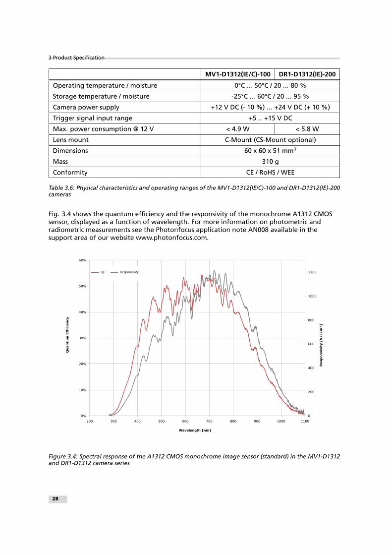
Table 3.6: Physical characteristics and operating ranges of the MV1-D1312(IE/C)-100 and DR1-D1312(IE)-200cameras
Fig. 3.4 shows the quantum efficiency and the responsivity of the monochrome A1312 CMOSsensor, displayed as a function of wavelength. For more information on photometric andradiometric measurements see the Photonfocus application note AN008 available in thesupport area of our website www.photonfocus.com.
800
1000
1200
30%
40%
50%
60%
V/
J/
m²]
m E
ffic
ien
cy
QE Responsivity
0
200
400
600
0%
10%
20%
30%
200 300 400 500 600 700 800 900 1000 1100
Resp
on
siv
ity [
V
Qu
an
tum
Wavelength [nm]
Figure 3.4: Spectral response of the A1312 CMOS monochrome image sensor (standard) in the MV1-D1312and DR1-D1312 camera series
28

Fig. 3.5 shows the quantum efficiency and the responsivity of the monochrome A1312IE CMOSsensor, displayed as a function of wavelength. The enhancement in the NIR quantum efficiencycould be used to realize applications in the 900 to 1064 nm region.
0%
10%
20%
30%
40%
50%
60%
300 400 500 600 700 800 900 1000 1100
Wavelength [nm]
Qu
an
tum
Eff
icie
ncy
0
200
400
600
800
1000
1200
Resp
on
siv
ity [
V/
J/
m^
2]
QE [%]
Responsivity [V/W/m^2]
Figure 3.5: Spectral response of the A1312IE monochrome image sensor (NIR enhanced) in the MV1-D1312IE and DR1-D1312IE camera series
.
3.3 Technical Specification 29

3 Product Specification
Fig. 3.6 shows the quantum efficiency and Fig. 3.7 the responsivity of the A1312C CMOS sensorused in the colour cameras, displayed as a function of wavelength. For more information onphotometric and radiometric measurements see the Photonfocus application notes AN006 andAN008 available in the support area of our website www.photonfocus.com.
0 %
5 %
1 0 %
1 5 %
2 0 %
2 5 %
3 0 %
3 5 %
4 0 %
4 5 %
3 0 0 4 0 0 5 0 0 6 0 0 7 0 0 8 0 0
W a v e l e n g t h [ n m ]
Quantu
m E
fficie
ncy
Q E ( r e d )
Q E ( g r e e n 1 )
Q E ( g r e e n 2 )
Q E ( b l u e )
Figure 3.6: Quantum efficiency of the A1312C CMOS image sensor in the MV1-D1312C colour camera series
0
1 0 0
2 0 0
3 0 0
4 0 0
5 0 0
6 0 0
7 0 0
8 0 0
9 0 0
3 0 0 4 0 0 5 0 0 6 0 0 7 0 0 8 0 0
W a v e l e n g t h [ n m ]
Responsivity [V/J/m
²]
R e s p o n s i v i t y ( r e d )
R e s p o n s i v i t y ( g r e e n 1 )
R e s p o n s i v i t y ( g r e e n 2 )
R e s p o n s i v i t y ( b l u e )
Figure 3.7: Responsivity of the A1312C CMOS image sensor in the MV1-D1312C colour camera series
.
30

The A1312C colour sensor is equipped with a cover glass. It incorporates an infra-red cut-offfilter to avoid false colours arising when an infra-red component is present in the illumination.Fig. 3.8 shows the transmssion curve of the cut-off filter.
Figure 3.8: Transmission curve of the cut-off filter in the MV1-D1312C colour camera series
.
3.3 Technical Specification 31

3 Product Specification
3.4 RGB Bayer Pattern Filter (colour models only)
Fig. 3.9 shows the bayer filter arrangement on the pixel matrix in the MV1-D1312C cameraseries. The numbers in the figure represents pixel position x, pixel position y.
The fix bayer pattern arrangement has to be considered when the ROI configu-ration is changed or the MROI feature is used (see 4.3). It depends on the linenumber in which an ROI starts. An ROI can start at an even or an odd line num-ber.
Figure 3.9: Bayer Pattern Arrangement in the MV1-D1312C camera series
32

4Functionality
This chapter serves as an overview of the camera configuration modes and explains camerafeatures. The goal is to describe what can be done with the camera. The setup of theMV1-D1312(IE/C) series cameras is explained in later chapters.
If not otherwise specified, the DR1-D1312(IE) camera series has the same func-tionality as the MV1-D1312(IE/C) camera series. In most cases only the MV1-D1312(IE/C) cameras are mentionend in the text.
4.1 Image Acquisition
4.1.1 Readout Modes
The MV1-D1312 CMOS cameras provide two different readout modes:
Sequential readout Frame time is the sum of exposure time and readout time. Exposure timeof the next image can only start if the readout time of the current image is finished.
Simultaneous readout (interleave) The frame time is determined by the maximum of theexposure time or of the readout time, which ever of both is the longer one. Exposuretime of the next image can start during the readout time of the current image.
Readout Mode MV1-D1312 Series
Sequential readout available
Simultaneous readout available
Table 4.1: Readout mode of MV1-D1312 Series camera
The following figure illustrates the effect on the frame rate when using either the sequentialreadout mode or the simultaneous readout mode (interleave exposure).
Sequential readout mode For the calculation of the frame rate only a single formula applies:frames per second equal to the inverse of the sum of exposure time and readout time.
Simultaneous readout mode (exposure time < readout time) The frame rate is given by thereadout time. Frames per second equal to the inverse of the readout time.
Simultaneous readout mode (exposure time > readout time) The frame rate is given by theexposure time. Frames per second equal to the inverse of the exposure time.
The simultaneous readout mode allows higher frame rates. However, if the exposure timegreatly exceeds the readout time, then the effect on the frame rate is neglectable.
In simultaneous readout mode image output faces minor limitations. The overalllinear sensor reponse is partially restricted in the lower grey scale region.
33

4 Functionality
E x p o s u r e t i m e
F r a m e r a t e
( f p s ) S i m u l t a n e o u s
r e a d o u t m o d e
S e q u e n t i a l
r e a d o u t m o d e
f p s = 1 / r e a d o u t t i m e
f p s = 1 / e x p o s u r e t i m e
f p s = 1 / ( r e a d o u t t i m e + e x p o s u r e t i m e )
e x p o s u r e t i m e < r e a d o u t t i m e e x p o s u r e t i m e > r e a d o u t t i m e
e x p o s u r e t i m e = r e a d o u t t i m e
Figure 4.1: Frame rate in sequential readout mode and simultaneous readout mode
When changing readout mode from sequential to simultaneous readout modeor vice versa, new settings of the BlackLevelOffset and of the image correctionare required.
Sequential readout
By default the camera continuously delivers images as fast as possible ("Free-running mode")in the sequential readout mode. Exposure time of the next image can only start if the readouttime of the current image is finished.
e x p o s u r e r e a d o u t e x p o s u r e r e a d o u t
Figure 4.2: Timing in free-running sequential readout mode
When the acquisition of an image needs to be synchronised to an external event, an externaltrigger can be used (refer to Section 4.4). In this mode, the camera is idle until it gets a signalto capture an image.
e x p o s u r e r e a d o u t i d l e e x p o s u r e
e x t e r n a l t r i g g e r
Figure 4.3: Timing in triggered sequential readout mode
Simultaneous readout (interleave exposure)
To achieve highest possible frame rates, the camera must be set to "Free-running mode" withsimultaneous readout. The camera continuously delivers images as fast as possible. Exposuretime of the next image can start during the readout time of the current image.
34

e x p o s u r e n i d l e i d l e
r e a d o u t n
e x p o s u r e n + 1
r e a d o u t n + 1
f r a m e t i m e
r e a d o u t n - 1
Figure 4.4: Timing in free-running simultaneous readout mode (readout time> exposure time)
e x p o s u r e n
i d l e r e a d o u t n
e x p o s u r e n + 1
f r a m e t i m e
r e a d o u t n - 1 i d l e
e x p o s u r e n - 1
Figure 4.5: Timing in free-running simultaneous readout mode (readout time< exposure time)
When the acquisition of an image needs to be synchronised to an external event, an externaltrigger can be used (refer to Section 4.4). In this mode, the camera is idle until it gets a signalto capture an image.
Figure 4.6: Timing in triggered simultaneous readout mode
4.1.2 Readout Timing
Sequential readout timing
By default, the camera is in free running mode and delivers images without any externalcontrol signals. The sensor is operated in sequential readout mode, which means that thesensor is read out after the exposure time. Then the sensor is reset, a new exposure starts andthe readout of the image information begins again. The data is output on the rising edge ofthe pixel clock. The signals FRAME_VALID (FVAL) and LINE_VALID (LVAL) mask valid imageinformation. The signal SHUTTER indicates the active exposure period of the sensor and is shownfor clarity only.
Simultaneous readout timing
To achieve highest possible frame rates, the camera must be set to "Free-running mode" withsimultaneous readout. The camera continuously delivers images as fast as possible. Exposuretime of the next image can start during the readout time of the current image. The data isoutput on the rising edge of the pixel clock. The signals FRAME_VALID (FVAL) and LINE_VALID (LVAL)
4.1 Image Acquisition 35

4 Functionality
P C L K
S H U T T E R
F V A L
L V A L
D V A L
D A T A
L i n e p a u s e L i n e p a u s e L i n e p a u s e
F i r s t L i n e L a s t L i n e
E x p o s u r eT i m e
F r a m e T i m e
C P R E
Figure 4.7: Timing diagram of sequential readout mode
mask valid image information. The signal SHUTTER indicates the active integration phase of thesensor and is shown for clarity only.
36

P C L K
S H U T T E R
F V A L
L V A L
D V A L
D A T A
L i n e p a u s e L i n e p a u s e L i n e p a u s e
F i r s t L i n e L a s t L i n e
E x p o s u r eT i m e
F r a m e T i m e
C P R E
E x p o s u r eT i m e
C P R E
Figure 4.8: Timing diagram of simultaneous readout mode (readout time > exposure time)
P C L K
S H U T T E R
F V A L
L V A L
D V A L
D A T A
L i n e p a u s e L i n e p a u s e L i n e p a u s e
F i r s t L i n e L a s t L i n e
F r a m e T i m e
C P R E
E x p o s u r e T i m e
C P R E
Figure 4.9: Timing diagram simultaneous readout mode (readout time < exposure time)
4.1 Image Acquisition 37

4 Functionality
Frame time Frame time is the inverse of the frame rate.
Exposure time Period during which the pixels are integrating the incoming light.
PCLK Pixel clock on internal camera interface.
SHUTTER Internal signal, shown only for clarity. Is ’high’ during the exposuretime.
FVAL (Frame Valid) Is ’high’ while the data of one complete frame are transferred.
LVAL (Line Valid) Is ’high’ while the data of one line are transferred. Example: To transferan image with 640x480 pixels, there are 480 LVAL within one FVAL activehigh period. One LVAL lasts 640 pixel clock cycles.
DVAL (Data Valid) Is ’high’ while data are valid.
DATA Transferred pixel values. Example: For a 100x100 pixel image, there are100 values transferred within one LVAL active high period, or 100*100values within one FVAL period.
Line pause Delay before the first line and after every following line when readingout the image data.
Table 4.2: Explanation of control and data signals used in the timing diagram
These terms will be used also in the timing diagrams of Section 4.4.
4.1.3 Exposure Control
The exposure time defines the period during which the image sensor integrates the incominglight. Refer to Section 3.3 for the allowed exposure time range.
4.1.4 Maximum Frame Rate
The maximum frame rate depends on the exposure time and the size of the image (see Section4.3.)
The maximal frame rate with current camera settings can be read out from theproperty FrameRateMax (AcquisitionFrameRateMax in GigE cameras).
.
38

4.2 Pixel Response
4.2.1 Linear Response
The camera offers a linear response between input light signal and output grey level. This canbe modified by the use of LinLog®as described in the following sections. In addition, a lineardigital gain may be applied, as follows. Please see Table 3.2 for more model-dependentinformation.
Black Level Adjustment
The black level is the average image value at no light intensity. It can be adjusted by thesoftware. Thus, the overall image gets brighter or darker. Use a histogram to control thesettings of the black level.
In CameraLink® cameras the black level is called "BlackLevelOffset" and in GigEcameras "BlackLevel".
4.2.2 LinLog®
Overview
The LinLog® technology from Photonfocus allows a logarithmic compression of high lightintensities inside the pixel. In contrast to the classical non-integrating logarithmic pixel, theLinLog® pixel is an integrating pixel with global shutter and the possibility to control thetransition between linear and logarithmic mode.
In situations involving high intrascene contrast, a compression of the upper grey level regioncan be achieved with the LinLog® technology. At low intensities each pixel shows a linearresponse. At high intensities the response changes to logarithmic compression (see Fig. 4.10).The transition region between linear and logarithmic response can be smoothly adjusted bysoftware and is continuously differentiable and monotonic.
LinLog® is controlled by up to 4 parameters (Time1, Time2, Value1 and Value2). Value1 and Value2correspond to the LinLog® voltage that is applied to the sensor. The higher the parametersValue1 and Value2 respectively, the stronger the compression for the high light intensities. Time1and Time2 are normalised to the exposure time. They can be set to a maximum value of 1000,which corresponds to the exposure time.
Examples in the following sections illustrate the LinLog® feature.
LinLog1
In the simplest way the pixels are operated with a constant LinLog® voltage which defines theknee point of the transition.This procedure has the drawback that the linear response curvechanges directly to a logarithmic curve leading to a poor grey resolution in the logarithmicregion (see Fig. 4.12).
.
4.2 Pixel Response 39

4 Functionality
G r e yV a l u e
L i g h t I n t e n s i t y
0 %
1 0 0 %
L i n e a r R e s p o n s e
S a t u r a t i o n
W e a k c o m p r e s s i o n
V a l u e 2
S t r o n g c o m p r e s s i o n
V a l u e 1
R e s u l t i n g L i n l o gR e s p o n s e
Figure 4.10: Resulting LinLog2 response curve
tt
V a l u e 1
t e x p
0
V L i n L o g
= V a l u e 2
T i m e 1 = T i m e 2 = m a x .= 1 0 0 0
Figure 4.11: Constant LinLog voltage in the Linlog1 mode
LinLog2
To get more grey resolution in the LinLog® mode, the LinLog2 procedure was developed. InLinLog2 mode a switching between two different logarithmic compressions occurs during theexposure time (see Fig. 4.13). The exposure starts with strong compression with a highLinLog®voltage (Value1). At Time1 the LinLog®voltage is switched to a lower voltage resulting ina weaker compression. This procedure gives a LinLog®response curve with more greyresolution. Fig. 4.14 and Fig. 4.15 show how the response curve is controlled by the threeparameters Value1, Value2 and the LinLog®time Time1.
Settings in LinLog2 mode, enable a fine tuning of the slope in the logarithmicregion.
LinLog3
To enable more flexibility the LinLog3 mode with 4 parameters was introduced. Fig. 4.16 showsthe timing diagram for the LinLog3 mode and the control parameters..
40

0
50
100
150
200
250
300
Typical LinLog1 Response Curve − Varying Parameter Value1
Illumination Intensity
Out
put g
rey
leve
l (8
bit)
[DN
]
V1 = 15
V1 = 16
V1 = 17
V1 = 18
V1 = 19
Time1=1000, Time2=1000, Value2=Value1
Figure 4.12: Response curve for different LinLog settings in LinLog1 mode
tt
V a l u e 1
V a l u e 2
T i m e 1
t e x p
0
V L i n L o g
T i m e 2 = m a x .= 1 0 0 0
T i m e 1
Figure 4.13: Voltage switching in the Linlog2 mode
4.2 Pixel Response 41

4 Functionality
0
50
100
150
200
250
300
Typical LinLog2 Response Curve − Varying Parameter Time1
Illumination Intensity
Out
put g
rey
leve
l (8
bit)
[DN
]
T1 = 840
T1 = 920
T1 = 960
T1 = 980
T1 = 999
Time2=1000, Value1=19, Value2=14
Figure 4.14: Response curve for different LinLog settings in LinLog2 mode
0
20
40
60
80
100
120
140
160
180
200
Typical LinLog2 Response Curve − Varying Parameter Time1
Illumination Intensity
Out
put g
rey
leve
l (8
bit)
[DN
]
T1 = 880T1 = 900T1 = 920T1 = 940T1 = 960T1 = 980T1 = 1000
Time2=1000, Value1=19, Value2=18
Figure 4.15: Response curve for different LinLog settings in LinLog2 mode
42

V L i n L o g
t
V a l u e 1
V a l u e 2
t e x p
T i m e 2
T i m e 1
T i m e 1 T i m e 2 t e x p
V a l u e 3 = C o n s t a n t = 0
Figure 4.16: Voltage switching in the LinLog3 mode
0
50
100
150
200
250
300
Typical LinLog2 Response Curve − Varying Parameter Time2
Illumination Intensity
Out
put g
rey
leve
l (8
bit)
[DN
]
T2 = 950 T2 = 960 T2 = 970
T2 = 980 T2 = 990
Time1=850, Value1=19, Value2=18
Figure 4.17: Response curve for different LinLog settings in LinLog3 mode
4.2 Pixel Response 43
4 Functionality
4.3 Reduction of Image Size
With Photonfocus cameras there are several possibilities to focus on the interesting parts of animage, thus reducing the data rate and increasing the frame rate. The most commonly usedfeature is Region of Interest (ROI).
4.3.1 Region of Interest (ROI)
Some applications do not need full image resolution (e.g. 1312 x 1082 pixels). By reducing theimage size to a certain region of interest (ROI), the frame rate can be increased. A region ofinterest can be almost any rectangular window and is specified by its position within the fullframe and its width (W) and height (H). Fig. 4.18, Fig. 4.19 and Fig. 4.20 show possibleconfigurations for the region of interest, and Table 4.3 presents numerical examples of howthe frame rate can be increased by reducing the ROI.
Both reductions in x- and y-direction result in a higher frame rate.
The minimum width of the region of interest depends on the camera model. Formore details please consult Table 4.5 and Table 4.7.
The minimum width must be positioned symmetrically towards the vertical cen-ter line of the sensor as shown in Fig. 4.18, Fig. 4.19 and Fig. 4.20). A list ofpossible settings of the ROI for each camera model is given in Table 4.7.
Colour models only: the vertical start position and height of every ROI should bean even number number to have the correct Bayer pattern in the output image(see also Section 3.4).
. It is recommended to re-adjust the settings of the shading correction each timea new region of interest is selected.
44

³ 1 4 4 P i x e l
³ 1 4 4 P i x e l
³ 1 4 4 P i x e l
+ m o d u l o 3 2 P i x e l
³ 1 4 4 P i x e l + m o d u l o 3 2 P i x e l
a ) b )
Figure 4.18: Possible configuration of the region of interest for the MV1-D1312(IE/C)-40 CMOS camera
³ 2 0 8 P i x e l
³ 2 0 8 P i x e l
³ 2 0 8 P i x e l
+ m o d u l o 3 2 P i x e l
³ 2 0 8 P i x e l + m o d u l o 3 2 P i x e l
a ) b )
Figure 4.19: Possible configuration of the region of interest with MV1-D1312(IE/C)-80 CMOS camera
Any region of interest may NOT be placed outside of the center of the sensor. Examples shownin Fig. 4.21 illustrate configurations of the ROI that are NOT allowed.
.
4.3 Reduction of Image Size 45

4 Functionality
³ 2 7 2 p i x e l
³ 2 7 2 p i x e l
³ 2 7 2 p i x e l
+ m o d u l o 3 2 p i x e l
³ 2 7 2 p i x e l + m o d u l o 3 2 p i x e l
a ) b )
Figure 4.20: Possible configuration of the region of interest with MV1-D1312(IE/C)-100 and DR1-D1312(IE)-200 CMOS cameras
ROI Dimension [Standard] MV1-D1312(IE/C)-40 MV1-D1312(IE/C)-80
1312 x 1082 (full resolution) 27 fps 54 fps
minimum resolution 10224 fps (288 x 1) 10672 fps (416 x 1)
1280 x 1024 (SXGA) 29 fps 58 fps
1280 x 768 (WXGA) 39 fps 78 fps
800 x 600 (SVGA) 78 fps 157 fps
640 x 480 (VGA) 121 fps 241 fps
544 x 1 9696 fps 10493 fps
544 x 1082 62 fps 125 fps
1312 x 544 53 fps 107 fps
1312 x 256 113 fps 227 fps
544 x 544 124 fps 248 fps
1024 x 1024 36 fps 72 fps
1312 x 1 8103 fps 9532 fps
Table 4.3: Frame rates of different ROI settings (exposure time 10 µs; correction on, and sequential readoutmode).
46

ROI Dimension [Standard] MV1-D1312(IE/C)-100 DR1-D1312(IE)-200 1)
1312 x 1082 (full resolution) 67 fps 135 fps
minimum resolution 10690 fps (544 x 1) 10766 fps (544 x 2)
1280 x 1024 (SXGA) 73 fps 146 fps
1280 x 768 (WXGA) 97 fps 194 fps
800 x 600 (SVGA) 195 fps 385 fps
640 x 480 (VGA) 300 fps 584 fps
544 x 1 10690 fps not allowed ROI setting
544 x 2 10066 fps 10766 fps
544 x 1082 157 fps 310 fps
1312 x 544 134 fps 266 fps
1312 x 256 282 fps 551 fps
544 x 544 308 fps 600 fps
1024 x 1024 90 fps 181 fps
1312 x 1 9879 fps not allowed ROI setting
Table 4.4: Frame rates of different ROI settings (exposure time 10 µs; correction on, and sequential readoutmode). (Footnotes: 1)double rate mode enabled).
a ) b )
Figure 4.21: ROI configuration examples that are NOT allowed
4.3 Reduction of Image Size 47
4 Functionality
4.3.2 ROI configuration
In the MV1-D1312(IE/C) camera series the following restrictions have to be respected for theROI configuration:
• The minimum width (w) of the ROI is camera model dependent, consisting of 288 pixel inthe MV1-D1312(IE/C)-40 camera, of 416 pixel in the MV1-D1312(IE/C)-80 camera and of544 pixel in the MV1-D1312(IE/C)-100 camera.
• The region of interest must overlap a minimum number of pixels centered to the left andto the right of the vertical middle line of the sensor (ovl).
• DR1-D1312(IE) cameras only: the height must be an even number.
For any camera model of the MV1-D1312(IE/C) camera series the allowed ranges for the ROIsettings can be deduced by the following formula:
xmin = max(0, 656 + ovl− w)xmax = min(656− ovl, 1312− w) .
where "ovl" is the overlap over the middle line and "w" is the width of the region of interest.
Any ROI settings in x-direction exceeding the minimum ROI width must be mod-ulo 32.
MV1-D1312(IE/C)-40 MV1-D1312(IE/C)-80
ROI width (w) 288 ... 1312 416 ... 1312
overlap (ovl) 144 208
width condition modulo 32 modulo 32
height condition 1 ... 1082 1 ... 1082
Table 4.5: Summary of the ROI configuration restrictions for the MV1-D1312(IE/C)-40 and MV1-D1312(IE/C)-80 cameras indicating the minimum ROI width (w) and the required number of pixel overlap (ovl) over thesensor middle line.
MV1-D1312(IE/C)-100 DR1-D1312(IE)-200
ROI width (w) 544 ... 1312 544 ... 1312
overlap (ovl) 272 272
width condition modulo 32 modulo 32
height condition 1 ... 1082 2 ... 1082, modulo 2
Table 4.6: Summary of the ROI configuration restrictions for the MV1-D1312(IE/C)-100 and DR1-D1312(IE)-200 cameras indicating the minimum ROI width (w) and the required number of pixel overlap (ovl) overthe sensor middle line.
The settings of the region of interest in x-direction are restricted to modulo 32(see Table 4.7).
48
There are no restrictions for the settings of the region of interest in y-directionin the MV1-D1312(IE/C) camera series. The ROI settings in y-direction for theDR1-D1312(IE)-200 camera is restricted to modulo 2.
Width ROI-X (MV1-D1312(IE/C)-40) ROI-X (MV1-D1312(IE/C)-80) ROI-X (-100 2), -200 3))
288 512 not available not available
320 480 ... 512 not available not available
352 448 ... 512 not available not available
384 416 ... 512 not available not available
416 384 ... 512 448 not available
448 352 ... 512 416 ... 448 not available
480 320 ... 520 384 ... 448 not available
512 288 ... 512 352 ... 448 not available
544 256 ...512 320 ... 448 384
576 224 ... 512 288 ... 448 352 ... 384
608 192 ... 512 256 ... 448 320 ... 352
640 160 ... 512 224 ... 448 288 ... 384
672 128 ... 512 192 ... 448 256 ... 384
704 96 ... 512 160 ... 448 224 ... 384
736 64 ... 512 128 ... 448 192 ... 384
768 32 ... 512 96 ... 448 160 ... 384
800 0 ... 512 64 ... 448 128 ... 384
832 0 ... 480 32 ... 448 96 ... 384
864 0 ... 448 0 ... 448 64 ... 384
896 0 ... 416 0 ... 416 32 ... 384
... ... ... ...
1312 0 0 0
Table 4.7: Some possible ROI-X settings (Footnotes: 2) MV1-D1312(IE/C)-100, 3) DR1-D1312(IE)-200)
.
4.3 Reduction of Image Size 49

4 Functionality
4.3.3 Calculation of the maximum frame rate
The frame rate mainly depends on the exposure time and readout time. The frame rate is theinverse of the frame time.
The maximal frame rate with current camera settings can be read out from theproperty FrameRateMax.
fps = 1tframe
Calculation of the frame time (sequential mode)
tframe ≥ texp + tro
Typical values of the readout time tro are given in table Table 4.8 and Table 4.9. Calculation ofthe frame time (simultaneous mode)
The calculation of the frame time in simultaneous read out mode requires more detailed datainput and is skipped here for the purpose of clarity.
ROI Dimension MV1-D1312(IE/C)-40 MV1-D1312(IE/C)-80 MV1-D1312(IE/C)-100
1312 x 1082 tro = 36.46 ms tro= 18.23 ms tro = 14.59 ms
1024 x 512 tro = 13.57 ms tro= 6.78 ms tro = 5.43 ms
1024 x 256 tro = 6.78 ms tro= 3.39 ms tro = 2.73 ms
Table 4.8: Read out time at different ROI settings for the MV1-D1312(IE/C) CMOS camera series in sequen-tial read out mode. (Footnotes: 1)double rate mode enabled).
ROI Dimension DR1-D1312(IE)-200
1312 x 1082 tro = 7.30 ms
1024 x 512 tro = 2.72 ms
1024 x 256 tro = 1.36 ms
Table 4.9: Read out time at different ROI settings for the DR1-D1312(IE) CMOS camera series in sequentialread out mode, double rate mode enabled.
A frame rate calculator for calculating the maximum frame rate is available inthe support area of the Photonfocus website.
An overview of resulting frame rates in different exposure time settings is given in table Table4.10 and Table 4.11.
50

Exposure time MV1-D1312(IE/C)-40 MV1-D1312(IE/C)-80 MV1-D1312(IE/C)-100
10 µs 27 / 27 fps 54 / 54 fps 67 / 67 fps
100 µs 27 / 27 fps 54 / 54 fps 67 / 67 fps
500 µs 27 / 27 fps 53 / 54 fps 65 / 67 fps
1 ms 27 / 27 fps 51 / 54 fps 63 / 67 fps
2 ms 26 / 27 fps 49 / 54 fps 60 / 67 fps
5 ms 24 / 27 fps 42 / 54 fps 50 / 67 fps
10 ms 22 / 27 fps 35 / 54 fps 40 / 67 fps
12 ms 21 / 27 fps 33 / 54 fps 37 / 67 fps
Table 4.10: Frame rates of different exposure times, [sequential readout mode / simultaneous readoutmode], resolution 1312 x 1082 pixel (correction on).
Exposure time DR1-D1312(IE)-200
10 µs 135 / 135 fps
100 µs 133 / 135 fps
500 µs 127 / 135 fps
1 ms 119 / 135 fps
2 ms 106 / 134 fps
5 ms 80 / 135 fps
10 ms 57 / 99 fps
12 ms 51 / 82 fps
Table 4.11: Frame rates of different exposure times, [sequential readout mode / simultaneous readoutmode], resolution 1312 x 1082 pixel (correction on), double rate mode enabled.
4.3 Reduction of Image Size 51

4 Functionality
4.3.4 Multiple Regions of Interest
The MV1-D1312(IE/C) camera series can handle up to 512 different regions of interest. Thisfeature can be used to reduce the image data and increase the frame rate. An applicationexample for using multiple regions of interest (MROI) is a laser triangulation system withseveral laser lines. The multiple ROIs are joined together and form a single image, which istransferred to the frame grabber.
An individual MROI region is defined by its starting value in y-direction and its height. Thestarting value in horizontal direction and the width is the same for all MROI regions and isdefined by the ROI settings. The maximum frame rate in MROI mode depends on the numberof rows and columns being read out. Overlapping ROIs are allowed. See Section 4.3.3 forinformation on the calculation of the maximum frame rate.
Fig. 4.22 compares ROI and MROI: the setups (visualized on the image sensor area) aredisplayed in the upper half of the drawing. The lower half shows the dimensions of theresulting image. On the left-hand side an example of ROI is shown and on the right-hand sidean example of MROI. It can be readily seen that resulting image with MROI is smaller than theresulting image with ROI only and the former will result in an increase in image frame rate.
ROI and MROI not only increase the frame rate but also the amount of data tobe processed is reduced. This increases the performance of your image procesingsystem.
M R O I 0
M R O I 1
M R O I 2
( 0 , 0 )
( 1 3 1 1 , 1 0 8 1 )
( 0 , 0 )
( 1 3 1 1 , 1 0 8 1 )
R O I
M R O I 0
M R O I 1
M R O I 2
R O I
Figure 4.22: Multiple Regions of Interest
Fig. 4.23 shows another MROI drawing illustrating the effect of MROI on the image content.
52

Figure 4.23: Multiple Regions of Interest with 5 ROIs
Fig. 4.24 shows an example from hyperspectral imaging where the presence of spectral lines atknown regions need to be inspected. By using MROI only a 656x54 region needs to be readoutand a frame rate of 4300 fps can be achieved. Without using MROI the resulting frame ratewould be 216 fps for a 656x1082 ROI.
6 3 6 p i x e l( 0 , 0 )
( xm a x
, ym a x
)
2 0 p i x e l
2 6 p i x e l
2 p i x e l
2 p i x e l
2 p i x e l
1 p i x e l
1 p i x e l
C h e m i c a l A g e n t A B C
Figure 4.24: Multiple Regions of Interest in hyperspectral imaging
4.3 Reduction of Image Size 53

4 Functionality
4.3.5 Decimation (monochrome models only)
Decimation reduces the number of pixels in y-direction. Decimation can also be used togetherwith ROI or MROI. Decimation in y-direction transfers every nthrow only and directly results inreduced read-out time and higher frame rate respectively.
Fig. 4.25 shows decimation on the full image. The rows that will be read out are marked by redlines. Row 0 is read out and then every nth row.
( 0 , 0 )
( 1 3 1 1 , 1 0 8 1 )
Figure 4.25: Decimation in full image
Fig. 4.26 shows decimation on a ROI. The row specified by the Window.Y setting is first readout and then every nth row until the end of the ROI.
( 0 , 0 )
( 1 3 1 1 , 1 0 8 1 )
R O I
Figure 4.26: Decimation and ROI
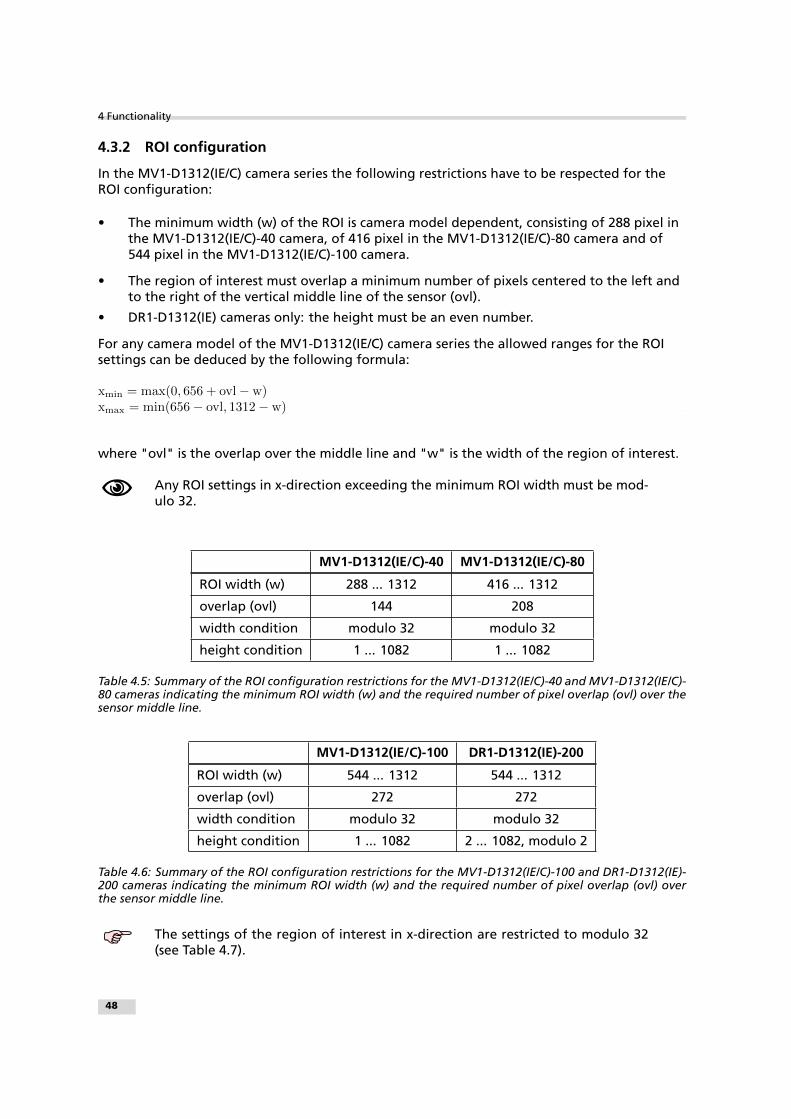
Fig. 4.27 shows decimation and MROI. For every MROI region m, the first row read out is therow specified by the MROI<m>.Y setting and then every nth row until the end of MROI regionm.
54
( 0 , 0 )
( 1 3 1 1 , 1 0 8 1 )
M R O I 0
R O I
M R O I 2
M R O I 1
Figure 4.27: Decimation and MROI
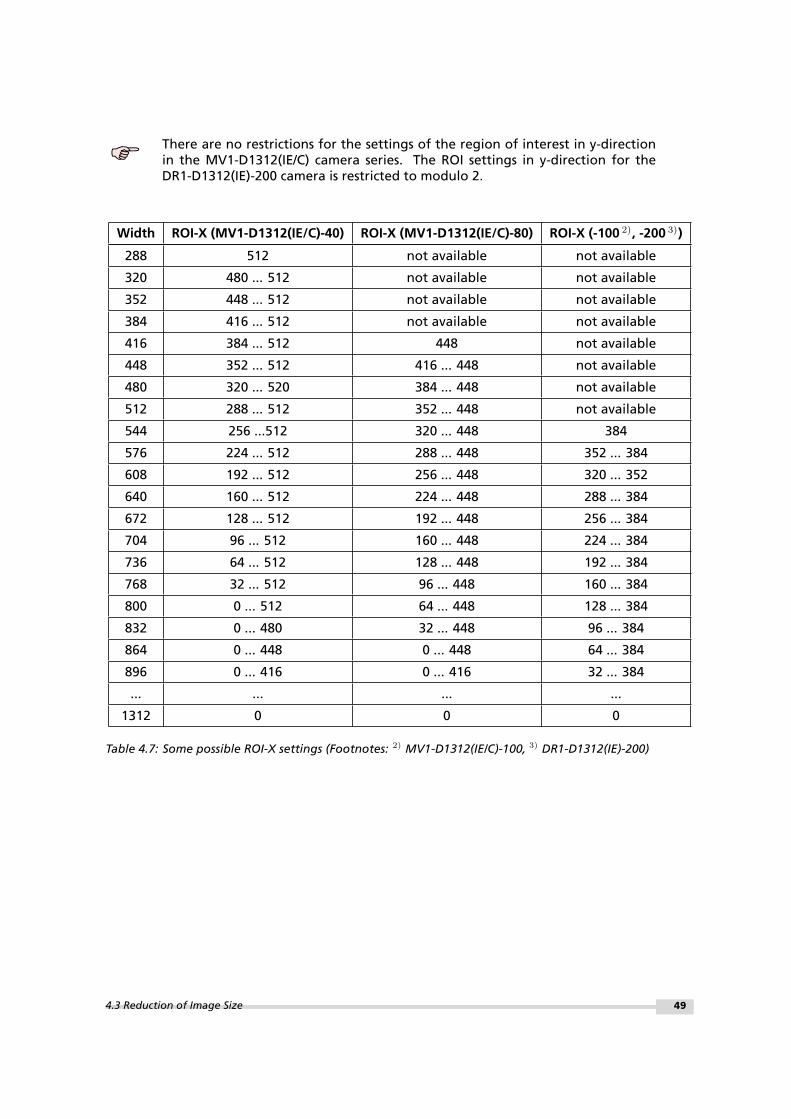
The image in Fig. 4.28 on the right-hand side shows the result of decimation 3 of the image onthe left-hand side.
Figure 4.28: Image example of decimation 3
An example of a high-speed measurement of the elongation of an injection needle is given inFig. 4.29. In this application the height information is less important than the widthinformation. Applying decimation 2 on the original image on the left-hand side doubles theresulting frame to about 7800 fps.
4.3 Reduction of Image Size 55

4 Functionality
Figure 4.29: Example of decimation 2 on image of injection needle
4.4 Trigger and Strobe
4.4.1 Introduction
The start of the exposure of the camera’s image sensor is controlled by the trigger. The triggercan either be generated internally by the camera (free running trigger mode) or by an externaldevice (external trigger mode).
This section refers to the external trigger mode if not otherwise specified.
In external trigger mode (TriggerMode=On), the trigger is applied according to the value of theTriggerSource property (see Section 4.4.2). The trigger signal can be configured to be activehigh or active low (property TriggerActivation). When the frequency of the incoming triggersis higher than the maximal frame rate of the current camera settings, then some trigger pulseswill be missed. A missed trigger counter counts these events. This counter can be read out bythe user. The input and output signals of the power connector are connected to theProgrammable Logic Controller (PLC) which allows powerful operations of the input andoutput signals (see Section 5.6).
A suitable trigger breakout cable for the Hirose 12 pol. connector can be orderedfrom your Photonfocus dealership.
The exposure time in external trigger mode can be defined by the setting of the exposure timeregister (camera controlled exposure mode) or by the width of the incoming trigger pulse(trigger controlled exposure mode) (see Section 4.4.4).
An external trigger pulse starts the exposure of one image. In Burst Trigger Mode however, atrigger pulse starts the exposure of a user defined number of images (see Section 4.4.6).
The start of the exposure is shortly after the active edge of the incoming trigger. An additionaltrigger delay can be applied that delays the start of the exposure by a user defined time (seeSection 4.4.5). This is often used to start the exposure after the trigger to a flash lightingsource.
4.4.2 Trigger Source
The trigger signal can be configured to be active high or active low by the TriggerActivation(category AcquisitionControl) property. One of the following trigger sources can be used:
Free running The trigger is generated internally by the camera. Exposure starts immediatelyafter the camera is ready and the maximal possible frame rate is attained, ifAcquisitionFrameRateEnable is disabled. Settings for free running trigger mode:TriggerMode = Off. In Constant Frame Rate mode (AcquisitionFrameRateEnable = True),exposure starts after a user-specified time has elapsed from the previous exposure start sothat the resulting frame rate is equal to the value of AcquisitionFrameRate.
56

Software Trigger The trigger signal is applied through a software command (TriggerSoftwarein category AcquisitionControl). Settings for Software Trigger mode: TriggerMode = Onand TriggerSource = Software.
Line1 Trigger The trigger signal is applied directly to the camera by the power supplyconnector through pin ISO_IN1 (see also Section A.1). A setup of this mode is shown inFig. 4.31 and Fig. 4.32. The electrical interface of the trigger input and the strobe outputis described in Section 5.5. Settings for Line1 Trigger mode: TriggerMode = On andTriggerSource = Line1.
PLC_Q4 Trigger The trigger signal is applied by the Q4 output of the PLC (see also Section 5.6).Settings for PLC_Q4 Trigger mode: TriggerMode = On and TriggerSource = PLC_Q4.
Some trigger signals are inverted. A schematic drawing is shown in Fig. 4.30.
I S O _ I N 0
I S O _ I N 1
P L C
L i n e 0
L i n e 1
P L C _ Q 1
P L C _ Q 4
I S O _ O U T 1
L i n e 1
S o f t w a r e T r i g g e r
C a m e r a
T r i g g e r
P L C _ Q 4
T r i g g e r S o u r c e
Figure 4.30: Trigger source schematic
.
4.4 Trigger and Strobe 57

4 Functionality
Figure 4.31: Trigger source
Figure 4.32: Trigger Inputs - Multiple GigE solution
58

4.4.3 Trigger and AcquisitionMode
The relationship between AcquisitionMode and TriggerMode is shown in Table 4.12. WhenTriggerMode=Off, then the frame rate depends on the AcquisitionFrameRateEnable property (seealso under Free running in Section 4.4.2).
The ContinuousRecording and ContinousReadout modes can be used if more thanone camera is connected to the same network and need to shoot images simul-taneously. If all camera are set to Continous mode, then all will send the packetsat same time resulting in network congestion. A better way would be to setthe cameras in ContinuousRecording mode and save the images in the memory ofthe IPEngine. The images can then be claimed with ContinousReadout from onecamera at a time avoid network collisions and congestion.
.
4.4 Trigger and Strobe 59

4 Functionality
AcquisitionMode TriggerMode After the command AcquisitionStart is executed:
Continuous Off Camera is in free-running mode. Acquisition can bestopped by executing AcquisitionStop command.
Continuous On Camera is ready to accept triggers according to theTriggerSource property. Acquisition and triggeracceptance can be stopped by executingAcquisitionStop command.
SingleFrame Off Camera acquires one frame and acquisition stops.
SingleFrame On Camera is ready to accept one trigger according tothe TriggerSource property. Acquisition and triggeracceptance is stopped after one trigger has beenaccepted.
MultiFrame Off Camera acquires n=AcquisitionFrameCount framesand acquisition stops.
MultiFrame On Camera is ready to accept n=AcquisitionFrameCounttriggers according to the TriggerSource property.Acquisition and trigger acceptance is stopped aftern triggers have been accepted.
SingleFrameRecording Off Camera saves one image on the onboard memoryof the IP engine.
SingleFrameRecording On Camera is ready to accept one trigger according tothe TriggerSource property. Trigger acceptance isstopped after one trigger has been accepted andimage is saved on the onboard memory of the IPengine.
SingleFrameReadout don’t care One image is acquired from the IP engine’sonboard memory. The image must have been savedin the SingleFrameRecording mode.
ContinuousRecording Off Camera saves images on the onboard memory ofthe IP engine until the memory is full.
ContinuousRecording On Camera is ready to accept triggers according to theTriggerSource property. Images are saved on theonboard memory of the IP engine until thememory is full. 18 images can be saved at fullresolution (1312x1082) in 8 bit mono mode.
ContinousReadout don’t care All Images that have been previously saved by theContinuousRecording mode are acquired from the IPengine’s onboard memory.
Table 4.12: AcquisitionMode and Trigger
60

4.4.4 Exposure Time Control
Depending on the trigger mode, the exposure time can be determined either by the camera orby the trigger signal itself:
Camera-controlled Exposure time In this trigger mode the exposure time is defined by thecamera. For an active high trigger signal, the camera starts the exposure with a positivetrigger edge and stops it when the preprogrammed exposure time has elapsed. Theexposure time is defined by the software.
Trigger-controlled Exposure time In this trigger mode the exposure time is defined by thepulse width of the trigger pulse. For an active high trigger signal, the camera starts theexposure with the positive edge of the trigger signal and stops it with the negative edge.
Trigger-controlled exposure time is not available in simultaneous readout mode.
External Trigger with Camera controlled Exposure Time
In the external trigger mode with camera controlled exposure time the rising edge of thetrigger pulse starts the camera states machine, which controls the sensor and optional anexternal strobe output. Fig. 4.33 shows the detailed timing diagram for the external triggermode with camera controlled exposure time.
e x t e r n a l t r i g g e r p u l s e i n p u t
t r i g g e r a f t e r i s o l a t o r
t r i g g e r p u l s e i n t e r n a l c a m e r a c o n t r o l
d e l a y e d t r i g g e r f o r s h u t t e r c o n t r o l
i n t e r n a l s h u t t e r c o n t r o l
d e l a y e d t r i g g e r f o r s t r o b e c o n t r o l
i n t e r n a l s t r o b e c o n t r o l
e x t e r n a l s t r o b e p u l s e o u t p u t
t d - i s o - i n p u t
t j i t t e r
t t r i g g e r - d e l a y
t e x p o s u r e
t s t r o b e - d e l a y
t d - i s o - o u t p u t
t s t r o b e - d u r a t i o n
t t r i g g e r - o f f s e t
t s t r o b e - o f f s e t
Figure 4.33: Timing diagram for the camera controlled exposure time
The rising edge of the trigger signal is detected in the camera control electronic which isimplemented in an FPGA. Before the trigger signal reaches the FPGA it is isolated from the
4.4 Trigger and Strobe 61
4 Functionality
camera environment to allow robust integration of the camera into the vision system. In thesignal isolator the trigger signal is delayed by time td−iso−input. This signal is clocked into theFPGA which leads to a jitter of tjitter. The pulse can be delayed by the time ttrigger−delay whichcan be configured by a user defined value via camera software. The trigger offset delayttrigger−offset results then from the synchronous design of the FPGA state machines. Theexposure time texposure is controlled with an internal exposure time controller.
The trigger pulse from the internal camera control starts also the strobe control state machines.The strobe can be delayed by tstrobe−delay with an internal counter which can be controlled bythe customer via software settings. The strobe offset delay tstrobe−delay results then from thesynchronous design of the FPGA state machines. A second counter determines the strobeduration tstrobe−duration(strobe-duration). For a robust system design the strobe output is alsoisolated from the camera electronic which leads to an additional delay of td−iso−output. Section4.4.6 gives an overview over the minimum and maximum values of the parameters.
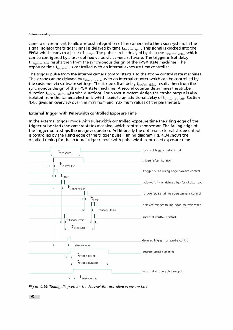
External Trigger with Pulsewidth controlled Exposure Time
In the external trigger mode with Pulsewidth controlled exposure time the rising edge of thetrigger pulse starts the camera states machine, which controls the sensor. The falling edge ofthe trigger pulse stops the image acquisition. Additionally the optional external strobe outputis controlled by the rising edge of the trigger pulse. Timing diagram Fig. 4.34 shows thedetailed timing for the external trigger mode with pulse width controlled exposure time.
e x t e r n a l t r i g g e r p u l s e i n p u t
t r i g g e r a f t e r i s o l a t o r
t r i g g e r p u l s e r i s i n g e d g e c a m e r a c o n t r o l
d e l a y e d t r i g g e r r i s i n g e d g e f o r s h u t t e r s e t
i n t e r n a l s h u t t e r c o n t r o l
d e l a y e d t r i g g e r f o r s t r o b e c o n t r o l
i n t e r n a l s t r o b e c o n t r o l
e x t e r n a l s t r o b e p u l s e o u t p u t
t d - i s o - i n p u t
t j i t t e r
t t r i g g e r - d e l a y
t e x p o s u r e
t s t r o b e - d e l a y
t d - i s o - o u t p u t
t s t r o b e - d u r a t i o n
t r i g g e r p u l s e f a l l i n g e d g e c a m e r a c o n t r o l
d e l a y e d t r i g g e r f a l l i n g e d g e s h u t t e r r e s e t
t j i t t e r
t t r i g g e r - d e l a y
t e x p o s u r e
t t r i g g e r - o f f s e t
t s t r o b e - o f f s e t
Figure 4.34: Timing diagram for the Pulsewidth controlled exposure time
62

The timing of the rising edge of the trigger pulse until to the start of exposure and strobe isequal to the timing of the camera controlled exposure time (see Section 4.4.4). In this modehowever the end of the exposure is controlled by the falling edge of the trigger Pulsewidth:
The falling edge of the trigger pulse is delayed by the time td−iso−input which is results from thesignal isolator. This signal is clocked into the FPGA which leads to a jitter of tjitter. The pulse isthen delayed by ttrigger−delay by the user defined value which can be configured via camerasoftware. After the trigger offset time ttrigger−offset the exposure is stopped.
4.4.5 Trigger Delay
The trigger delay is a programmable delay in milliseconds between the incoming trigger edgeand the start of the exposure. This feature may be required to synchronize to external strobewith the exposure of the camera.
4.4.6 Burst Trigger
The camera includes a burst trigger engine. When enabled, it starts a predefined number ofacquisitions after one single trigger pulse. The time between two acquisitions and the numberof acquisitions can be configured by a user defined value via the camera software. The bursttrigger feature works only in the mode "Camera controlled Exposure Time".
The burst trigger signal can be configured to be active high or active low. When the frequencyof the incoming burst triggers is higher than the duration of the programmed burst sequence,then some trigger pulses will be missed. A missed burst trigger counter counts these events.This counter can be read out by the user.
The burst trigger mode is only available when TriggerMode=On. Trigger source is determined bythe TriggerSource property.The timing diagram of the burst trigger mode is shown in Fig. 4.35. The timing of the"external trigger pulse input" until to the "trigger pulse internal camera control" is equal tothe timing in the section Fig. 4.34. This trigger pulse then starts after a user configurable bursttrigger delay time tburst−trigger−delay the internal burst engine, which generates n internaltriggers for the shutter- and the strobe-control. A user configurable value defines the timetburst−period−time between two acquisitions.
.
4.4 Trigger and Strobe 63

4 Functionality
e x t e r n a l t r i g g e r p u l s e i n p u t
t r i g g e r a f t e r i s o l a t o r
t r i g g e r p u l s e i n t e r n a l c a m e r a c o n t r o l
d e l a y e d t r i g g e r f o r s h u t t e r c o n t r o l
i n t e r n a l s h u t t e r c o n t r o l
d e l a y e d t r i g g e r f o r s t r o b e c o n t r o l
i n t e r n a l s t r o b e c o n t r o l
e x t e r n a l s t r o b e p u l s e o u t p u t
t d - i s o - i n p u t
t j i t t e r
t t r i g g e r - d e l a y
t e x p o s u r e
t s t r o b e - d e l a y
t d - i s o - o u t p u t
t s t r o b e - d u r a t i o n
t t r i g g e r - o f f s e t
t s t r o b e - o f f s e t
d e l a y e d t r i g g e r f o r b u r s t t r i g g e r e n g i n e
t b u r s t - t r i g g e r - d e l a y
t b u r s t - p e r i o d - t i m e
Figure 4.35: Timing diagram for the burst trigger mode
64

MV1-D1312(IE/C)-40 MV1-D1312(IE/C)-40
Timing Parameter Minimum Maximum
td−iso−input 1 µs 1.5 µs
td−RS422−input 65 ns 185 ns
tjitter 0 100 ns
ttrigger−delay 0 1.68 s
tburst−trigger−delay 0 1.68 s
tburst−period−time depends on camera settings 1.68 s
ttrigger−offset (non burst mode) 400 ns 400 ns
ttrigger−offset (burst mode) 500 ns 500 ns
texposure 10 µs 1.68 s
tstrobe−delay 0 1.68 s
tstrobe−offset (non burst mode) 400 ns 400 ns
tstrobe−offset (burst mode) 500 ns 500 ns
tstrobe−duration 200 ns 1.68 s
td−iso−output 150 ns 350 ns
ttrigger−pulsewidth 200 ns n/a
Number of bursts n 1 30000
Table 4.13: Summary of timing parameters relevant in the external trigger mode using camera MV1-D1312(IE/C)-40
4.4 Trigger and Strobe 65

4 Functionality
MV1-D1312(IE/C)-80 MV1-D1312(IE/C)-80
Timing Parameter Minimum Maximum
td−iso−input 1 µs 1.5 µs
td−RS422−input 65 ns 185 ns
tjitter 0 50 ns
ttrigger−delay 0 0.84 s
tburst−trigger−delay 0 0.84 s
tburst−period−time depends on camera settings 0.84 s
ttrigger−offset (non burst mode) 200 ns 200 ns
ttrigger−offset (burst mode) 250 ns 250 ns
texposure 10 µs 0.84 s
tstrobe−delay 600 ns 0.84 s
tstrobe−offset (non burst mode) 200 ns 200 ns
tstrobe−offset (burst mode) 250 ns 250 ns
tstrobe−duration 200 ns 0.84 s
td−iso−output 150 ns 350 ns
ttrigger−pulsewidth 200 ns n/a
Number of bursts n 1 30000
Table 4.14: Summary of timing parameters relevant in the external trigger mode using camera MV1-D1312(IE/C)-80
66

MV1-D1312(IE/C)-100 MV1-D1312(IE/C)-100
Timing Parameter Minimum Maximum
td−iso−input 1 µs 1.5 µs
td−RS422−input 65 ns 185 ns
tjitter 0 40 ns
ttrigger−delay 0 0.67 s
tburst−trigger−delay 0 0.67 s
tburst−period−time depends on camera settings 0.67 s
ttrigger−offset (non burst mode) 160 ns 160 ns
ttrigger−offset (burst mode) 200 ns 200 ns
texposure 10 µs 0.67 s
tstrobe−delay 0 0.67 s
tstrobe−offset (non burst mode) 160 ns 160 ns
tstrobe−offset (burst mode) 200 ns 200 ns
tstrobe−duration 200 ns 0.67 s
td−iso−output 150 ns 350 ns
ttrigger−pulsewidth 200 ns n/a
Number of bursts n 1 30000
Table 4.15: Summary of timing parameters relevant in the external trigger mode using camera MV1-D1312(IE/C)-100
4.4 Trigger and Strobe 67

4 Functionality
DR1-D1312(IE)-200 DR1-D1312(IE)-200
Timing Parameter Minimum Maximum
td−iso−input 1 µs 1.5 µs
td−RS422−input 65 ns 185 ns
tjitter 0 20 ns
ttrigger−delay 0 0.33 s
tburst−trigger−delay 0 0.33 s
tburst−period−time depends on camera settings 0.33 s
ttrigger−offset (non burst mode) 80 ns 80 ns
ttrigger−offset (burst mode) 100 ns 100 ns
texposure 10 µs 0.33 s
tstrobe−delay 0 0.33 s
tstrobe−offset (non burst mode) 80 ns 80 ns
tstrobe−offset (burst mode) 100 ns 100 ns
tstrobe−duration 200 ns 0.33 s
td−iso−output 150 ns 350 ns
ttrigger−pulsewidth 200 ns n/a
Number of bursts n 1 30000
Table 4.16: Summary of timing parameters relevant in the external trigger mode using camera DR1-D1312(IE)-200
68

4.4.7 Software Trigger
The software trigger enables to emulate an external trigger pulse by the camera softwarethrough the serial data interface. It works with both burst mode enabled and disabled. Assoon as it is performed via the camera software, it will start the image acquisition(s),depending on the usage of the burst mode and the burst configuration. The trigger modemust be set to external Trigger (TriggerMode = On).
4.4.8 Strobe Output
The strobe output is an isolated output located on the power supply connector that can beused to trigger a strobe. The strobe output can be used both in free-running and in triggermode. There is a programmable delay available to adjust the strobe pulse to your application.
The strobe output needs a separate power supply. Please see Section 5.5, Fig.4.31 and Fig. 4.32 for more information.
.
4.4 Trigger and Strobe 69

4 Functionality
4.5 Data Path Overview
The data path is the path of the image from the output of the image sensor to the output ofthe camera. The sequence of blocks is shown in figure Fig. 4.36.
I m a g e S e n s o r
F P N C o r r e c t i o n
D i g i t a l O f f s e t
D i g i t a l G a i n
L o o k - u p t a b l e ( L U T )
3 x 3 C o n v o l v e r
C r o s s h a i r s i n s e r t i o n
S t a t u s l i n e i n s e r t i o n
T e s t i m a g e s i n s e r t i o n
A p p l y d a t a r e s o l u t i o n
I m a g e o u t p u t
M o n o c h r o m e c a m e r a s
I m a g e S e n s o r
F P N C o r r e c t i o n
D i g i t a l O f f s e t
D i g i t a l G a i n /
R G B F i n e G a i n
L o o k - u p t a b l e ( L U T )
S t a t u s l i n e i n s e r t i o n
T e s t i m a g e s i n s e r t i o n
A p p l y d a t a r e s o l u t i o n
I m a g e o u t p u t
C o l o u r c a m e r a s
Figure 4.36: camera data path
.
70

4.6 Image Correction
4.6.1 Overview
The camera possesses image pre-processing features, that compensate for non-uniformitiescaused by the sensor, the lens or the illumination. This method of improving the image qualityis generally known as ’Shading Correction’ or ’Flat Field Correction’ and consists of acombination of offset correction, gain correction and pixel interpolation.
Since the correction is performed in hardware, there is no performance limita-tion of the cameras for high frame rates.
The offset correction subtracts a configurable positive or negative value from the live imageand thus reduces the fixed pattern noise of the CMOS sensor. In addition, hot pixels can beremoved by interpolation. The gain correction can be used to flatten uneven illumination or tocompensate shading effects of a lens. Both offset and gain correction work on a pixel-per-pixelbasis, i.e. every pixel is corrected separately. For the correction, a black reference and a greyreference image are required. Then, the correction values are determined automatically in thecamera.
Do not set any reference images when gain or LUT is enabled! Read the follow-ing sections very carefully.
Correction values of both reference images can be saved into the internal flash memory, butthis overwrites the factory presets. Then the reference images that are delivered by factorycannot be restored anymore.
4.6.2 Offset Correction (FPN, Hot Pixels)
The offset correction is based on a black reference image, which is taken at no illumination(e.g. lens aperture completely closed). The black reference image contains the fixed-patternnoise of the sensor, which can be subtracted from the live images in order to minimise thestatic noise.
Offset correction algorithm
After configuring the camera with a black reference image, the camera is ready to apply theoffset correction:
1. Determine the average value of the black reference image.
2. Subtract the black reference image from the average value.
3. Mark pixels that have a grey level higher than 1008 DN (@ 12 bit) as hot pixels.
4. Store the result in the camera as the offset correction matrix.
5. During image acquisition, subtract the correction matrix from the acquired image andinterpolate the hot pixels (see Section 4.6.2).
4.6 Image Correction 71

4 Functionality
4
4
4
31
21
3 1
4 32
3
4
1
1
2 4 14
4
3
1
3
4
b l a c k r e f e r e n c e
i m a g e
1
1
1
2- 1
2- 2
- 1 0
1 - 11
- 1
0
2
0
- 1
0
- 2
0
1 1 - 2 - 2 - 2
a v e r a g e
o f b l a c k
r e f e r e n c e
p i c t u r e
=-
o f f s e t c o r r e c t i o n
m a t r i x
Figure 4.37: Schematic presentation of the offset correction algorithm
How to Obtain a Black Reference Image
In order to improve the image quality, the black reference image must meet certain demands.
The detailed procedure to set the black reference image is described in Section6.5.
• The black reference image must be obtained at no illumination, e.g. with lens apertureclosed or closed lens opening.
• It may be necessary to adjust the black level offset of the camera. In the histogram of theblack reference image, ideally there are no grey levels at value 0 DN after adjustment ofthe black level offset. All pixels that are saturated black (0 DN) will not be properlycorrected (see Fig. 4.38). The peak in the histogram should be well below the hot pixelthreshold of 1008 DN @ 12 bit.
• Camera settings may influence the grey level. Therefore, for best results the camerasettings of the black reference image must be identical with the camera settings of theimage to be corrected.
0 200 400 600 800 1000 1200 1400 16000
0.2
0.4
0.6
0.8
1Histogram of the uncorrected black reference image
Grey level, 12 Bit [DN]
Rel
ativ
e nu
mbe
r of
pix
els
[−]
black level offset okblack level offset too low
Figure 4.38: Histogram of a proper black reference image for offset correction
72

Hot pixel correction
Every pixel that exceeds a certain threshold in the black reference image is marked as a hotpixel. If the hot pixel correction is switched on, the camera replaces the value of a hot pixel byan average of its neighbour pixels (see Fig. 4.39).
h o t
p i x e l
pn
pn - 1
pn + 1
pn =
pn - 1+ p
n + 1
2
Figure 4.39: Hot pixel interpolation
4.6.3 Gain Correction
The gain correction is based on a grey reference image, which is taken at uniform illuminationto give an image with a mid grey level.
Gain correction is not a trivial feature. The quality of the grey reference imageis crucial for proper gain correction.
Gain correction algorithm
After configuring the camera with a black and grey reference image, the camera is ready toapply the gain correction:
1. Determine the average value of the grey reference image.
2. Subtract the offset correction matrix from the grey reference image.
3. Divide the average value by the offset corrected grey reference image.
4. Pixels that have a grey level higher than a certain threshold are marked as hot pixels.
5. Store the result in the camera as the gain correction matrix.
6. During image acquisition, multiply the gain correction matrix from the offset-correctedacquired image and interpolate the hot pixels (see Section 4.6.2).
Gain correction is not a trivial feature. The quality of the grey reference imageis crucial for proper gain correction.
4.6 Image Correction 73
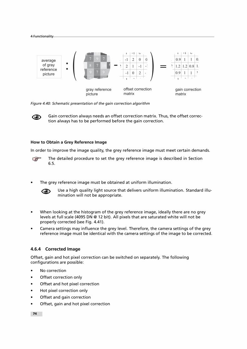
4 Functionality
:7
1 0
9
79
78
7 9
4 32
3
4
1
1
9 6 84
6
1 0
1
3
4
g r a y r e f e r e n c e
p i c t u r e
a v e r a g e
o f g r a y
r e f e r e n c e
p i c t u r e) 1
1 . 2
1
0 . 9 1
1 . 2- 2
0 . 9 1
1 - 11
0 . 8
1
1
0
1 . 3
0 . 8
1
0
1 1 - 2 - 2 - 2
=
1
1
1
2- 1
2- 2
- 1 0
1 - 11
- 1
0
2
0
- 1
0
- 2
0
1 1 - 2 - 2 - 2
- )o f f s e t c o r r e c t i o n
m a t r i x
g a i n c o r r e c t i o n
m a t r i x
Figure 4.40: Schematic presentation of the gain correction algorithm
Gain correction always needs an offset correction matrix. Thus, the offset correc-tion always has to be performed before the gain correction.
How to Obtain a Grey Reference Image
In order to improve the image quality, the grey reference image must meet certain demands.
The detailed procedure to set the grey reference image is described in Section6.5.
• The grey reference image must be obtained at uniform illumination.
Use a high quality light source that delivers uniform illumination. Standard illu-mination will not be appropriate.
• When looking at the histogram of the grey reference image, ideally there are no greylevels at full scale (4095 DN @ 12 bit). All pixels that are saturated white will not beproperly corrected (see Fig. 4.41).
• Camera settings may influence the grey level. Therefore, the camera settings of the greyreference image must be identical with the camera settings of the image to be corrected.
4.6.4 Corrected Image
Offset, gain and hot pixel correction can be switched on separately. The followingconfigurations are possible:
• No correction
• Offset correction only
• Offset and hot pixel correction
• Hot pixel correction only
• Offset and gain correction
• Offset, gain and hot pixel correction
74

2400 2600 2800 3000 3200 3400 3600 3800 4000 42000
0.2
0.4
0.6
0.8
1Histogram of the uncorrected grey reference image
Grey level, 12 Bit [DN]
Rel
ativ
e nu
mbe
r of
pix
els
[−]
grey reference image okgrey reference image too bright
Figure 4.41: Proper grey reference image for gain correction
5
7
6
57
66
5 6
4 37
3
4
7
1
7 4 64
4
3
1
3
4
c u r r e n t i m a g e
) 5
6
6
55
65
5 4
4 37
3
4
7
1
7 4 64
4
3
1
3
4
)1
1
1
2- 1
2- 2
- 1 0
1 - 11
- 1
0
2
0
- 1
0
- 2
0
1 1 - 2 - 2 - 2
o f f s e t c o r r e c t i o n
m a t r i x
-1
1 . 2
1
0 . 9 1
1 . 2- 2
0 . 9 1
1 - 11
0 . 8
1
1
0
1 . 3
0 . 8
1
0
1 1 - 2 - 2 - 2
g a i n c o r r e c t i o n
m a t r i x
=.
c o r r e c t e d i m a g e
)Figure 4.42: Schematic presentation of the corrected image using gain correction algorithm
In addition, the black reference image and grey reference image that are currently stored inthe camera RAM can be output.Table 4.17 shows the minimum and maximum values of the correction matrices, i.e. the rangethat the offset and gain algorithm can correct.
Minimum Maximum
Offset correction -1023 DN @ 12 bit +1023 DN @ 12 bit
Gain correction 0.42 2.67
Table 4.17: Offset and gain correction ranges
.
4.6 Image Correction 75

4 Functionality
4.7 Digital Gain and Offset
There are two different gain settings on the camera:
Gain (Digital Fine Gain) Digital fine gain accepts fractional values from 0.01 up to 15.99. It isimplemented as a multiplication operation. Colour camera models only: There isadditionally a gain for every RGB colour channel. The RGB channel gain is used tocalibrate the white balance in an image, which has to be set according to the currentlighting condition.
Digital Gain Digital Gain is a coarse gain with the settings x1, x2, x4 and x8. It is implementedas a binary shift of the image data where ’0’ is shifted to the LSB’s of the gray values. E.g.for gain x2, the output value is shifted by 1 and bit 0 is set to ’0’.
The resulting gain is the product of the two gain values, which means that the image data ismultiplied in the camera by this factor.
Digital Fine Gain and Digital Gain may result in missing codes in the output im-age data.
A user-defined value can be subtracted from the gray value in the digital offset block. If digitalgain is applied and if the brightness of the image is too big then the interesting part of theoutput image might be saturated. By subtracting an offset from the input of the gain block itis possible to avoid the saturation.
4.8 Grey Level Transformation (LUT)
Grey level transformation is remapping of the grey level values of an input image to newvalues. The look-up table (LUT) is used to convert the greyscale value of each pixel in an imageinto another grey value. It is typically used to implement a transfer curve for contrastexpansion. The camera performs a 12-to-8-bit mapping, so that 4096 input grey levels can bemapped to 256 output grey levels. The use of the three available modes is explained in thenext sections. Two LUT and a Region-LUT feature are available in the MV1-D1312 camera series(see Section 4.8.4).
For the MV1-D1312-240-CL camera series, bits 0 & 1 of the LUT input are fixed to0.
The output grey level resolution of the look-up table (independent of gain,gamma or user-definded mode) is always 8 bit.
There are 2 predefined functions, which generate a look-up table and transfer itto the camera. For other transfer functions the user can define his own LUT file.
Some commonly used transfer curves are shown in Fig. 4.43. Line a denotes a negative orinverse transformation, line b enhances the image contrast between grey values x0 and x1.Line c shows brightness thresholding and the result is an image with only black and white greylevels. and line d applies a gamma correction (see also Section 4.8.2).
76

a
y = f ( x )
xxm a x
x0
x1
ym a x
b
c
d
Figure 4.43: Commonly used LUT transfer curves
4.8.1 Gain
The ’Gain’ mode performs a digital, linear amplification with clamping (see Fig. 4.44). It isconfigurable in the range from 1.0 to 4.0 (e.g. 1.234).
0 200 400 600 800 1000 12000
50
100
150
200
250
300Grey level transformation − Gain: y = (255/1023) ⋅ a ⋅ x
x: grey level input value (10 bit) [DN]
y: g
rey
leve
l out
put v
alue
(8
bit)
[DN
]
a = 1.0a = 2.0a = 3.0a = 4.0
Figure 4.44: Applying a linear gain with clamping to an image
4.8 Grey Level Transformation (LUT) 77

4 Functionality
4.8.2 Gamma
The ’Gamma’ mode performs an exponential amplification, configurable in the range from 0.4to 4.0. Gamma > 1.0 results in an attenuation of the image (see Fig. 4.45), gamma < 1.0 resultsin an amplification (see Fig. 4.46). Gamma correction is often used for tone mapping andbetter display of results on monitor screens.
0 200 400 600 800 1000 12000
50
100
150
200
250
300Grey level transformation − Gamma: y = (255 / 1023γ) ⋅ xγ (γ ≥ 1)
x: grey level input value (10 bit) [DN]
y: g
rey
leve
l out
put v
alue
(8
bit)
[DN
]
γ = 1.0γ = 1.2γ = 1.5γ = 1.8γ = 2.5γ = 4.0
Figure 4.45: Applying gamma correction to an image (gamma > 1)
0 200 400 600 800 1000 12000
50
100
150
200
250
300Grey level transformation − Gamma: y = (255 / 1023γ) ⋅ xγ (γ ≤ 1)
x: grey level input value (10 bit) [DN]
y: g
rey
leve
l out
put v
alue
(8
bit)
[DN
]
γ = 1.0γ = 0.9γ = 0.8γ = 0.6γ = 0.4
Figure 4.46: Applying gamma correction to an image (gamma < 1)
78

4.8.3 User-defined Look-up Table
In the ’User’ mode, the mapping of input to output grey levels can be configured arbitrarily bythe user. There is an example file in the PFRemote folder. LUT files can easily be generatedwith a standard spreadsheet tool. The file has to be stored as tab delimited text file.
U s e r L U T
y = f ( x )
1 2 b i t 8 b i t
Figure 4.47: Data path through LUT
4.8.4 Region LUT and LUT Enable
Two LUTs and a Region-LUT feature are available in the MV1-D1312(IE/C) camera series. BothLUTs can be enabled independently (see Table 4.18). LUT 0 superseds LUT1.
Enable LUT 0 Enable LUT 1 Enable Region LUT Description
- - - LUT are disabled.
X don’t care - LUT 0 is active on whole image.
- X - LUT 1 is active on whole image.
X - X LUT 0 active in Region 0.
X X X LUT 0 active in Region 0 and LUT 1 active
in Region 1. LUT 0 supersedes LUT1.
Table 4.18: LUT Enable and Region LUT
4.8 Grey Level Transformation (LUT) 79

4 Functionality
When the Region-LUT feature is enabled, then the LUTs are only active in a user definedregion. Examples are shown in Fig. 4.48 and Fig. 4.49.
Fig. 4.48 shows an example of overlapping Region-LUTs. LUT 0, LUT 1 and Region LUT areenabled. LUT 0 is active in region 0 ((x00, x01), (y00, y01)) and it supersedes LUT 1 in theoverlapping region. LUT 1 is active in region 1 ((x10, x11), (y10, y11)).
L U T 0
( 0 , 0 )
( 1 3 1 1 , 1 0 8 1 )
L U T 1
x 0 0 x 1 0 x 0 1 x 1 1
y 1 0
y 0 0
y 0 1
y 1 1
Figure 4.48: Overlapping Region-LUT example
Fig. 4.49 shows an example of keyhole inspection in a laser welding application. LUT 0 and LUT1 are used to enhance the contrast by applying optimized transfer curves to the individualregions. LUT 0 is used for keyhole inspection. LUT 1 is optimized for seam finding.
L U T 0
( 0 , 0 )
( 1 3 1 1 , 1 0 8 1 )
L U T 1
( 0 , 0 )
( 1 3 1 1 , 1 0 8 1 )
L U T 1
L U T 0
Figure 4.49: Region-LUT in keyhole inspection
.
80

Fig. 4.50 shows the application of the Region-LUT to a camera image. The original imagewithout image processing is shown on the left-hand side. The result of the application of theRegion-LUT is shown on the right-hand side. One Region-LUT was applied on a small region onthe lower part of the image where the brightness has been increased.
Figure 4.50: Region-LUT example with camera image; left: original image; right: gain 4 region in the areof the date print of the bottle
.
4.8 Grey Level Transformation (LUT) 81

4 Functionality
4.9 Convolver (monochrome models only)
4.9.1 Functionality
The "Convolver" is a discrete 2D-convolution filter with a 3x3 convolution kernel. The kernelcoefficients can be user-defined.
The M x N discrete 2D-convolution pout(x,y) of pixel pin(x,y) with convolution kernel h, scale sand offset o is defined in Fig. 4.51.
Figure 4.51: Convolution formula
4.9.2 Settings
The following settings for the parameters are available:
Offset Offset value o (see Fig. 4.51). Range: -4096 ... 4095
Scale Scaling divisor s (see Fig. 4.51). Range: 1 ... 4095
Coefficients Coefficients of convolution kernel h (see Fig. 4.51). Range: -4096 ... 4095.Assignment to coefficient properties is shown in Fig. 4.52.
Figure 4.52: Convolution coefficients assignment
4.9.3 Examples
Fig. 4.53 shows the result of the application of various standard convolver settings to theoriginal image. shows the corresponding settings for every filter.
.
82

Figure 4.53: 3x3 Convolution filter examples 1
Figure 4.54: 3x3 Convolution filter examples 1 settings
4.9 Convolver (monochrome models only) 83

4 Functionality
A filter called Unsharp Mask is often used to enhance near infrared images. Fig. 4.55 showsexamples with the corresponding settings.
Figure 4.55: Unsharp Mask Examples
.
84

4.10 Crosshairs (monochrome models only)
4.10.1 Functionality
The crosshairs inserts a vertical and horizontal line into the image. The width of these lines isone pixel. The grey level is defined by a 12 bit value (0 means black, 4095 means white). Thisallows to set any grey level to get the maximum contrast depending on the acquired image.The x/y position and the grey level can be set via the camera software. Figure Fig. 4.56 showstwo examples of the activated crosshairs with different grey values. One with white lines andthe other with black lines.
Figure 4.56: Crosshairs Example with different grey values
.
4.10 Crosshairs (monochrome models only) 85

4 Functionality
The x- and y-positon is absolute to the sensor pixel matrix. It is independent on the ROI, MROIor decimation configurations. Figure Fig. 4.57 shows two situations of the crosshairsconfiguration. The same MROI settings is used in both situations. The crosshairs however is setdifferently. The crosshairs is not seen in the image on the right, because the x- and y-position isset outside the MROI region.
( 0 , 0 )
( 1 3 1 1 , 1 0 8 1 )
( xa b s o l u t
, ya b s o l u t
, G r e y L e v e l )
M R O I 0
M R O I 1
( 0 , 0 )
( 1 3 1 1 , 1 0 8 1 )
M R O I 0
M R O I 1
( xa b s o l u t
, ya b s o l u t
, G r e y L e v e l )
M R O I 0
M R O I 1
M R O I 0
M R O I 1
Figure 4.57: Crosshairs absolute position
.
86

4.11 Image Information and Status Line (not available for DR1-D1312(IE))
There are camera properties available that give information about the acquired images, suchas an image counter, average image value and the number of missed trigger signals. Theseproperties can be queried by software. Alternatively, a status line within the image data can beswitched on that contains all the available image information.
4.11.1 Counters and Average Value
Image counter The image counter provides a sequential number of every image that is output.After camera startup, the counter counts up from 0 (counter width 24 bit). The countercan be reset by the camera control software.
Real Time counter The time counter starts at 0 after camera start, and counts real-time in unitsof 1 micro-second. The time counter can be reset by the software in the SDK (Counterwidth 32 bit).
Missed trigger counter The missed trigger counter counts trigger pulses that were ignored bythe camera because they occurred within the exposure or read-out time of an image. Infree-running mode it counts all incoming external triggers (counter width 8 bit / no wraparound).
Missed burst trigger counter The missed burst trigger counter counts trigger pulses that wereignored by the camera in the burst trigger mode because they occurred while the camerastill was processing the current burst trigger sequence.
Average image value The average image value gives the average of an image in 12 bit format(0 .. 4095 DN), regardless of the currently used grey level resolution.
4.11.2 Status Line
If enabled, the status line replaces the last row of the image with camera status information.Every parameter is coded into fields of 4 pixels (LSB first) and uses the lower 8 bits of the pixelvalue, so that the total size of a parameter field is 32 bit (see Fig. 4.58). The assignment of theparameters to the fields is listed in Table 4.19.
The status line is available in all camera modes.
4 8 1 2 1 6 2 0
P r e a m b l e F i e l d 0
0P i x e l : 1 2 3 5 6 7 9 1 0 1 1 1 3 1 4 1 5 1 7 1 8 1 9 2 1 2 2 2 3
L S B M S B
F F 0 0 A A 5 5
F i e l d 1 F i e l d 2 F i e l d 3 F i e l d 4
L S B L S B L S B L S B L S BM S B M S B M S B M S B M S B
Figure 4.58: Status line parameters replace the last row of the image
.
4.11 Image Information and Status Line (not available for DR1-D1312(IE)) 87
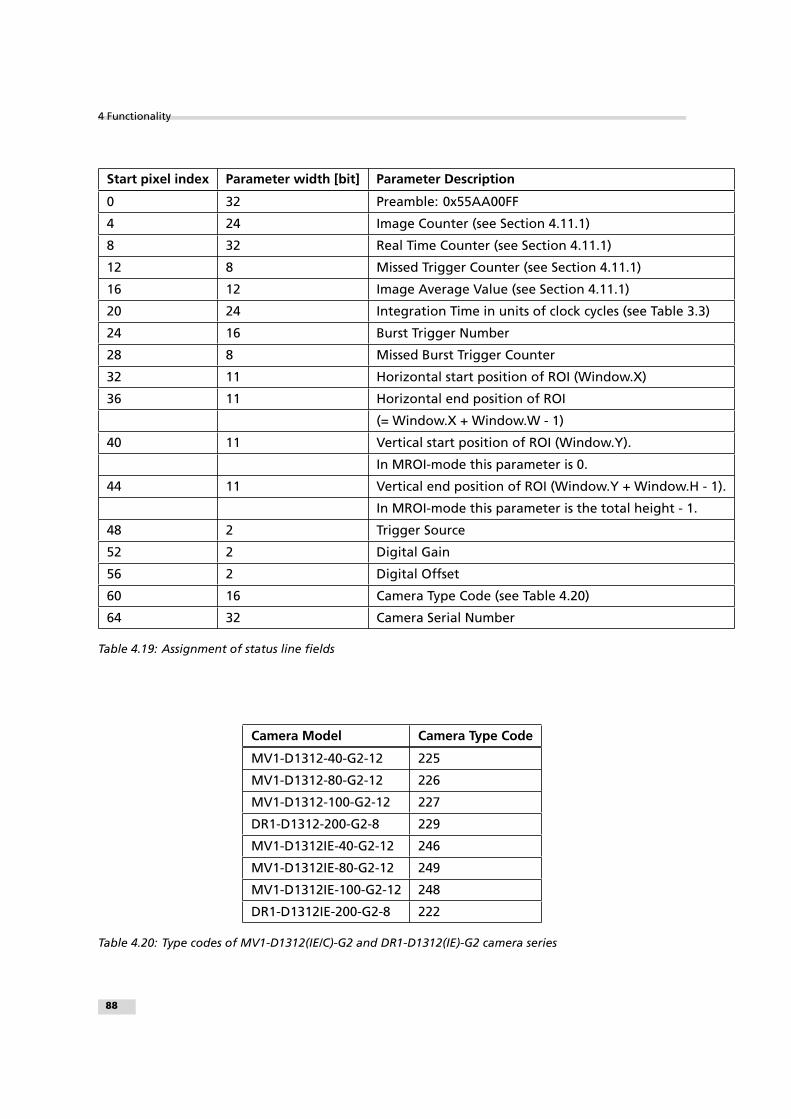
4 Functionality
Start pixel index Parameter width [bit] Parameter Description
0 32 Preamble: 0x55AA00FF
4 24 Image Counter (see Section 4.11.1)
8 32 Real Time Counter (see Section 4.11.1)
12 8 Missed Trigger Counter (see Section 4.11.1)
16 12 Image Average Value (see Section 4.11.1)
20 24 Integration Time in units of clock cycles (see Table 3.3)
24 16 Burst Trigger Number
28 8 Missed Burst Trigger Counter
32 11 Horizontal start position of ROI (Window.X)
36 11 Horizontal end position of ROI
(= Window.X + Window.W - 1)
40 11 Vertical start position of ROI (Window.Y).
In MROI-mode this parameter is 0.
44 11 Vertical end position of ROI (Window.Y + Window.H - 1).
In MROI-mode this parameter is the total height - 1.
48 2 Trigger Source
52 2 Digital Gain
56 2 Digital Offset
60 16 Camera Type Code (see Table 4.20)
64 32 Camera Serial Number
Table 4.19: Assignment of status line fields
Camera Model Camera Type Code
MV1-D1312-40-G2-12 225
MV1-D1312-80-G2-12 226
MV1-D1312-100-G2-12 227
DR1-D1312-200-G2-8 229
MV1-D1312IE-40-G2-12 246
MV1-D1312IE-80-G2-12 249
MV1-D1312IE-100-G2-12 248
DR1-D1312IE-200-G2-8 222
Table 4.20: Type codes of MV1-D1312(IE/C)-G2 and DR1-D1312(IE)-G2 camera series
88
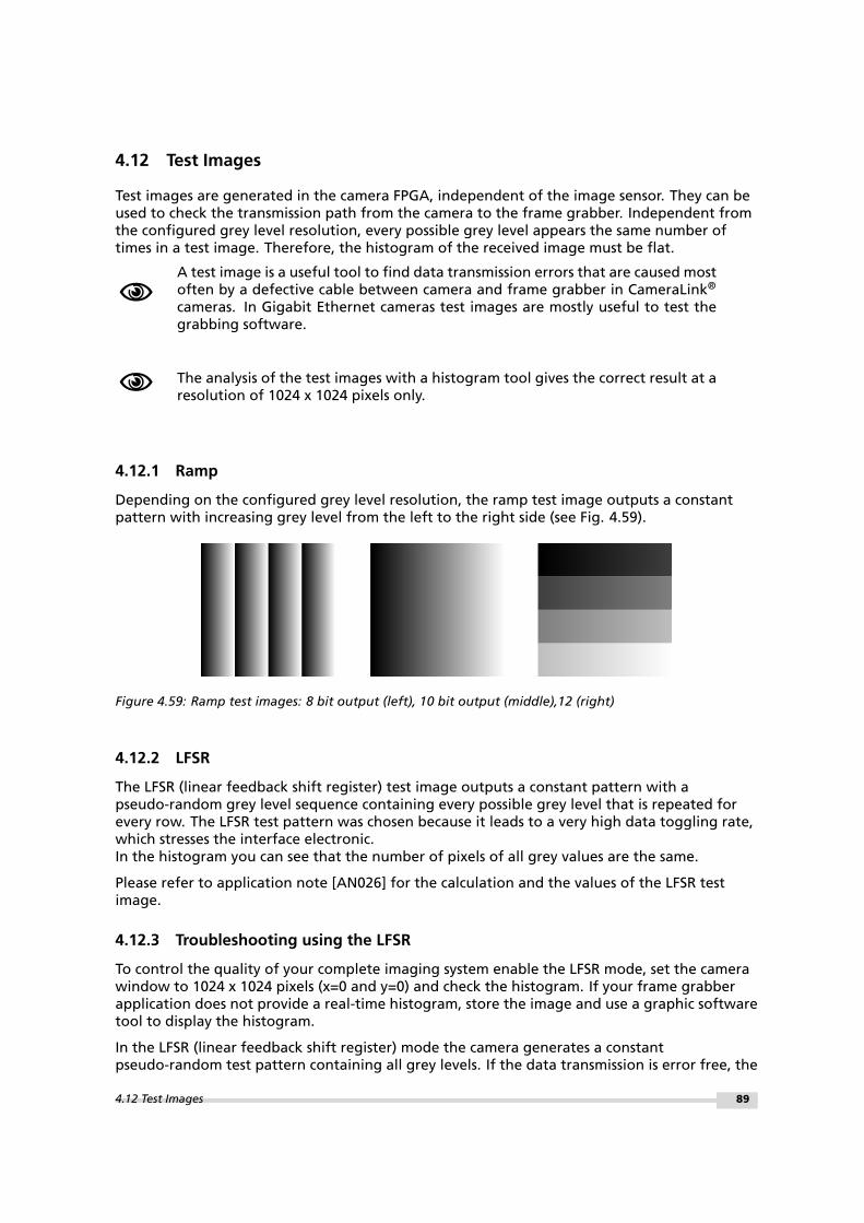
4.12 Test Images
Test images are generated in the camera FPGA, independent of the image sensor. They can beused to check the transmission path from the camera to the frame grabber. Independent fromthe configured grey level resolution, every possible grey level appears the same number oftimes in a test image. Therefore, the histogram of the received image must be flat.
A test image is a useful tool to find data transmission errors that are caused mostoften by a defective cable between camera and frame grabber in CameraLink®
cameras. In Gigabit Ethernet cameras test images are mostly useful to test thegrabbing software.
The analysis of the test images with a histogram tool gives the correct result at aresolution of 1024 x 1024 pixels only.
4.12.1 Ramp
Depending on the configured grey level resolution, the ramp test image outputs a constantpattern with increasing grey level from the left to the right side (see Fig. 4.59).
Figure 4.59: Ramp test images: 8 bit output (left), 10 bit output (middle),12 (right)
4.12.2 LFSR
The LFSR (linear feedback shift register) test image outputs a constant pattern with apseudo-random grey level sequence containing every possible grey level that is repeated forevery row. The LFSR test pattern was chosen because it leads to a very high data toggling rate,which stresses the interface electronic.In the histogram you can see that the number of pixels of all grey values are the same.
Please refer to application note [AN026] for the calculation and the values of the LFSR testimage.
4.12.3 Troubleshooting using the LFSR
To control the quality of your complete imaging system enable the LFSR mode, set the camerawindow to 1024 x 1024 pixels (x=0 and y=0) and check the histogram. If your frame grabberapplication does not provide a real-time histogram, store the image and use a graphic softwaretool to display the histogram.
In the LFSR (linear feedback shift register) mode the camera generates a constantpseudo-random test pattern containing all grey levels. If the data transmission is error free, the
4.12 Test Images 89
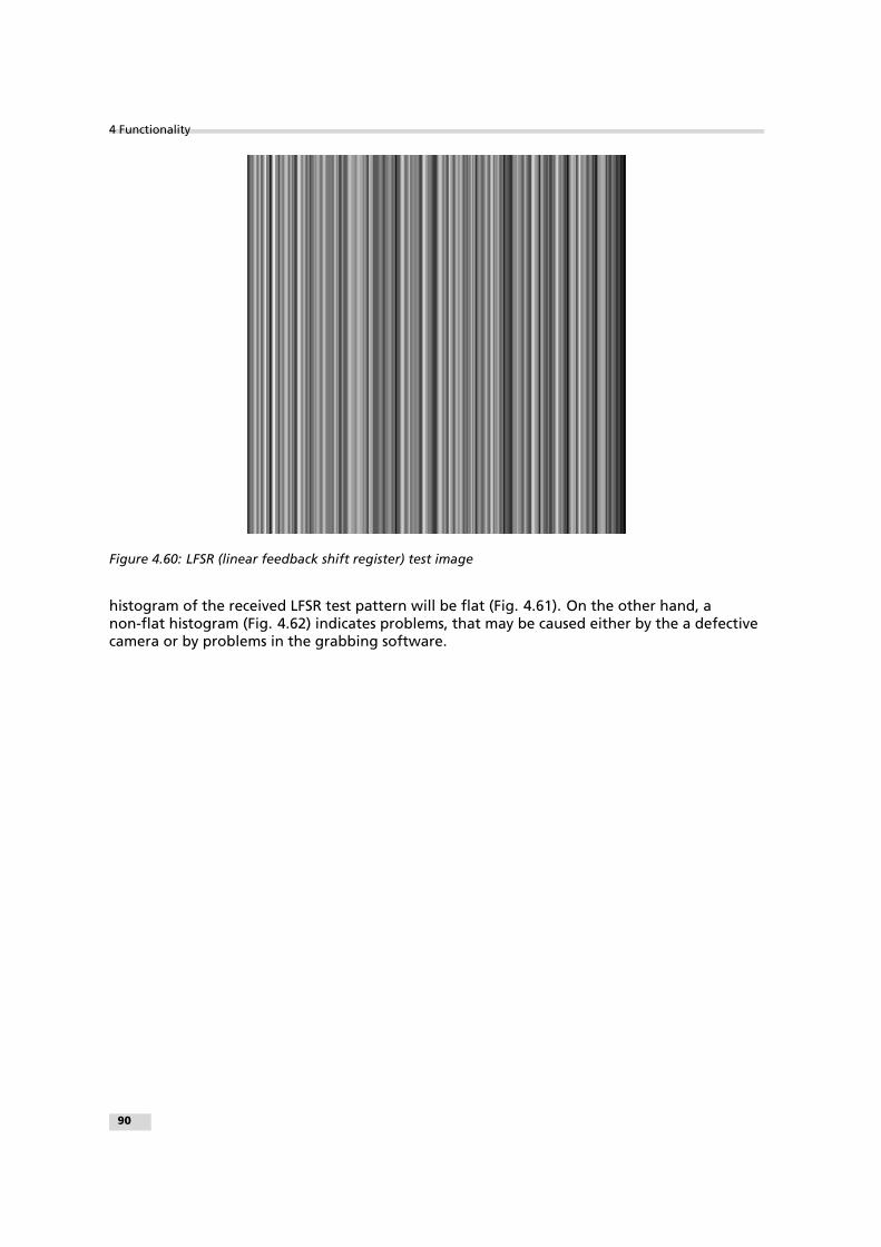
4 Functionality
Figure 4.60: LFSR (linear feedback shift register) test image
histogram of the received LFSR test pattern will be flat (Fig. 4.61). On the other hand, anon-flat histogram (Fig. 4.62) indicates problems, that may be caused either by the a defectivecamera or by problems in the grabbing software.
.
90

Figure 4.61: LFSR test pattern received and typical histogram for error-free data transmission
Figure 4.62: LFSR test pattern received and histogram containing transmission errors
In robots applications, the stress that is applied to the camera cable is especially high due tothe fast movement of the robot arm. For such applications, special drag chain capable cablesare available. Please contact the Photonfocus Support for consulting expertise. .
.
4.12 Test Images 91

4 Functionality
4.13 Double Rate (DR1-D1312(IE) only)
The Photonfocus DR1 cameras use a proprietary modulation algorithm to cut the data rate byalmost a factor of two. This enables the transmission of high frame rates over just one GigabitEthernet connection, avoiding the complexity and stability issues of Ethernet link aggregation.The algorithm is lossy but no image artefacts are introduced, unlike for example the JPEGcompression. It is therefore very well suited for most machine vision applications except formeasuring tasks where sub-pixel precision is required.
Double rate modulation can be turned off for debugging purposes.
The modulated image is transmitted in mono 8 bit data resolution.
The modulation is run in real-time in the camera’s FPGA. A DLL for the demodulation of theimage for SDK applications is included in the GEV-Player software package that can bedownloaded from Photonfocus (see also 6).
The modulation factor is independent of the image content. The modulated image has thesame number of rows as the unmodulated image. The required image width (number of bytesin a row) for the modulated image can be calculated as follows (value can also be read from acamera property), see also Table 4.21:
wmod = ceil(w/64) + w/2 + 2
92

Width unmodulated Width modulated
544 283
576 299
608 316
640 332
672 349
704 365
736 382
768 398
800 415
832 431
864 448
896 464
928 481
960 497
992 514
1024 530
1056 547
1088 563
1120 580
1152 596
1184 613
1216 629
1248 646
1280 662
1312 679
Table 4.21: Width of modulated image in double rate mode
4.13 Double Rate (DR1-D1312(IE) only) 93

4 Functionality
94

5Hardware Interface
5.1 GigE Connector
The GigE cameras are interfaced to external components via
• an Ethernet jack (RJ45) to transmit configuration, image data and trigger.
• a 12 pin subminiature connector for the power supply, Hirose HR10A-10P-12S (female) .
The connectors are located on the back of the camera. Fig. 5.1 shows the plugs and the statusLED which indicates camera operation.
P o w e r S u p p l y
a n d I / O C o n n e c t o rS t a t u s L E D
E t h e r n e t J a c k
( R J 4 5 )
Figure 5.1: Rear view of the GigE camera
5.2 Power Supply Connector
The camera requires a single voltage input (see Table 3.5). The camera meets all performancespecifications using standard switching power supplies, although well-regulated linear powersupplies provide optimum performance.
It is extremely important that you apply the appropriate voltages to your camera.Incorrect voltages will damage the camera.
A suitable power supply can be ordered from your Photonfocus dealership.
For further details including the pinout please refer to Appendix A.
95

5 Hardware Interface
5.3 Status Indicator (GigE cameras)
A dual-color LED on the back of the camera gives information about the current status of theGigE CMOS cameras.
LED Green Green when an image is output. At slow frame rates, the LED blinks with theFVAL signal. At high frame rates the LED changes to an apparently continuousgreen light, with intensity proportional to the ratio of readout time over frametime.
LED Red Red indicates an active serial communication with the camera.
Table 5.1: Meaning of the LED of the GigE CMOS cameras
5.4 Power and Ground Connection for GigE G2 Cameras
The interface electronics is isolated from the camera electronics and the power supplyincluding the line filters and camera case. Fig. 5.2 shows a schematic of the power and groundconnections.
.
96

P o w e r S u p p l y
2
P O W E R _ R E T U R N
1
C A S E
G N D
I n t e r n a l P o w e r S u p p l y
D C / D C V C C _ 3
+
P O W E R
R X R S 4 2 2I S O _ I N C 0 _ P
I S O _ I N C 0 _ N
I S O _ I N C 1 _ P
I S O _ I N C 1 _ N
I S O _ I N 0
I S O _ I N 1
I S O _ O U T 0
I S O _ O U T 1
Isolated Interface
Camera
Electronic
I S O L A T O R
I S O _ G N D
I S O _ P W R
1 2
12 pol. H
irose C
onnector
6
8
3
9
7
1 0
1 1
4
5
+
I / O a n d T r i g g e r I n t e r f a c e
D C / D C
D C / D C
V C C _ 2
V C C _ 1
ESD
Pro
tection
ESD
Pro
tection
Camera
Electronic
Line
Filter
Y O U R _ G N D
Y O U R _ P W R+
Hirose C
onnector
C A S E
G N D
C a m e r a
Figure 5.2: Schematic of power and ground connections
5.4 Power and Ground Connection for GigE G2 Cameras 97

5 Hardware Interface
5.5 Trigger and Strobe Signals for GigE G2 Cameras
5.5.1 Overview
The 12-pol. Hirose power connector contains two external trigger inputs, two strobe outputsand two differential RS-422 inputs. All inputs and outputs are connected to the ProgrammableLogic Controller (PLC) (see also Section 5.6) that offers powerful operations.
The pinout of the power connector is described in Section A.1.
ISO_INC0 and ISO_INC1 RS-422 inputs have -10 V to +13 V extended commonmode range.
ISO_OUT0 and ISO_OUT1 have different output circuits (see also Section 5.5.2).
A suitable trigger breakout cable for the Hirose 12 pol. connector can be orderedfrom your Photonfocus dealership.
Simulation with LTSpice is possible, a simulation model can be downloaded fromour web site www.photonfocus.com on the software download page (in Supportsection). It is filed under "Third Party Tools".
Fig. 5.3 shows the schematic of the inputs and outputs. All inputs and outputs are isolated.ISO_VCC is an isolated, internally generated voltage.
.
98

I S O _ G N D
R X R S 4 2 2I S O _ I N C 0 _ P
I S O _ I N C 0 _ N
M A X 3 0 9 8
I S O _ I N C 1 _ P
I S O _ I N C 1 _ N
I S O _ G N D
I S O _ V C C
e n h a n c e d
P o w e r F E T4 . 7 V
1 0 kI S O _ I N 0
G N D I S O _ G N D
I S O _ V C C
e n h a n c e d
P o w e r F E T4 . 7 V
1 0 kI S O _ I N 1
I S O _ G N D
I S O _ P W R
P o w e r
M O S F E T
I S O _ O U T 0P T C 4 k 7
M a x . 3 0 V
M a x . 0 . 5 A
M a x . 0 . 5 W
I S O _ G N D
P o w e r
M O S F E T
I S O _ O U T 1P T C
M a x . 3 0 V
M a x . 0 . 5 A
M a x . 0 . 5 W
Isolated Interface
Camera
Electronic
- 1 0 V t o + 1 3 V e x t e n d e d
C o m m o n M o d e R a n g e
I S O L A T O R
I S O _ G N D
I S O _ P W R
1 2
12 pol. H
irose C
onnector
6
8
3
9
7
1 0
1 1
4
5
+
+
+
+
C a m e r a
M i n . - 3 0 V
M a x . 3 0 V
M i n . - 3 0 V
M a x . 3 0 V
I S O _ V C C+
Figure 5.3: Schematic of inputs and output
5.5 Trigger and Strobe Signals for GigE G2 Cameras 99

5 Hardware Interface
5.5.2 Single-ended Inputs
ISO_IN0 and ISO_IN1 are single-ended isolated inputs. The input circuit of both inputs isidentical (see Fig. 5.3).
Fig. 5.4 shows a direct connection to the ISO_IN inputs.
In the camera default settings the PLC is configured to connect the ISO_IN0 tothe PLC_Q4 camera trigger input. This setting is listed in Section 6.10.2.
I S O _ G N D I S O _ G N D
I S O _ V C C
e n h a n c e d
P o w e r F E T4 . 7 V
1 0 kI S O _ I N 0
C a m e r a
7
1 2 p o l . H i r o s e
C o n n e c t o r
I S O _ G N D
1 2
Y O U R _ G N D Y O U R _ G N D
I n p u t V o l t a g e
M a x . + 3 0 V D C
M i n . - 3 0 V D C
+
Figure 5.4: Direct connection to ISO_IN
Fig. 5.5 shows how to connect ISO_IN to TTL logic output device.
I S O _ G N D I S O _ G N D
I S O _ V C C
e n h a n c e d
P o w e r F E T4 . 7 V
1 0 kI S O _ I N 0
C a m e r a
7
1 2 p o l . H i r o s e
C o n n e c t o r
I S O _ G N D
1 2
Y O U R _ G N D Y O U R _ G N D
C o n t r o l L o g i c
&
Y O U R _ V C C +
+
Figure 5.5: Connection to ISO_IN from a TTL logic device
.
100

5.5.3 Single-ended Outputs
ISO_OUT0 and ISO_OUT1 are single-ended isolated outputs.
ISO_OUT0 and ISO_OUT1 have different output circuits: ISO_OUT1 doesn’t havea pullup resistor and can be used as additional Strobe out (by adding Pull up) oras controllable switch. Maximal ratings that must not be exceeded: voltage: 30V, current: 0.5 A, power: 0.5 W.
Fig. 5.6 shows the connection from the ISO_OUT0 output to a TTL logic device. PTC is a currentlimiting device.
I S O _ G N D
I S O _ P W R
P o w e r
M O S F E T
I S O _ O U T 0P T C4 k 7
C a m e r a
3
1 2 p o l . H i r o s e
C o n n e c t o r
I S O _ G N D
1 2
Y O U R _ G N D
I S O _ P W R Y O U R _ P W R
Y O U R _ G N D
C o n t r o l L o g i c
&
Y O U R _ P W R+ + + +6
M a x . 3 0 V
M a x . 0 . 5 A
M a x . 0 . 5 W
Figure 5.6: Connection example to ISO_OUT0
Fig. 5.7 shows the connection from ISO_OUT1 to a TTL logic device. PTC is a current limitingdevice.
I S O _ G N D
P o w e r
M O S F E T
I S O _ O U T 1P T C
C a m e r a
8
1 2 p o l . H i r o s e
C o n n e c t o r
I S O _ G N D
1 2
Y O U R _ G N D Y O U R _ G N D
C o n t r o l L o g i c
&
Y O U R _ P W R+
4 k 7
+
Y O U R _ P W R
M a x . 3 0 V
M a x . 0 . 5 A
M a x . 0 . 5 W
Figure 5.7: Connection from the ISO_OUT1 output to a TTL logic device
.
5.5 Trigger and Strobe Signals for GigE G2 Cameras 101

5 Hardware Interface
Fig. 5.8 shows the connection from ISO_OUT1 to a LED.
Y O U R _ P W R
I S O _ G N D
P o w e r
M O S F E T
I S O _ O U T 1P T C R
C a m e r a
8
1 2 p o l . H i r o s e
C o n n e c t o r
I S O _ G N D
1 2
Y O U R _ G N D
+
Figure 5.8: Connection from ISO_OUT1 to a LED
Respect the limits of the POWER MOSFET in the connection to ISEO_OUT1. Max-imal ratings that must not be exceeded: voltage: 30 V, current: 0.5 A, power: 0.5W. (see also Fig. 5.9). The type of the Power MOSFET is: International RectifierIRLML0100TRPbF.
Y O U R _ P W R
I S O _ G N D
P o w e r
M O S F E T
I S O _ O U T 1P T C
L
C a m e r a
8
1 2 p o l . H i r o s e
C o n n e c t o r
I S O _ G N D
1 2
Y O U R _ G N D
Y O U R _ P W R
LDD
D
1
2
M a x . 3 0 V
M a x . 0 . 5 A
M a x . 0 . 5 W
+ +
R e s p e c t t h e l i m i t s o f t h e P O W E R M O S F E T !
Figure 5.9: Limits of ISO_OUT1 output
.
102

5.5.4 Differential RS-422 Inputs
ISO_INC0 and ISO_INC1 are isolated differential RS-422 inputs (see also Fig. 5.3). They areconnected to a Maxim MAX3098 RS-422 receiver device. Please consult the data sheet of theMAX3098 for connection details.
Don’t connect single-ended signals to the differential inputs ISO_INC0 andISO_INC1 (see also Fig. 5.10).
R X R S 4 2 2
I S O _ I N C x _ P
I S O _ I N C x _ N
1 2 p o l . H i r o s e
C o n n e c t o r
Y O U R _ G N D
5 V T T L L o g i c L e v e l
C a m e r a
Figure 5.10: Incorrect connection to ISO_INC inputs
5.5.5 Master / Slave Camera Connection
The trigger input of one Photonfocus G2 camera can easily connected to the strobe output ofanother Photonfocus G2 camera as shown in Fig. 5.11. This results in a master/slave modewhere the slave camera operates synchronously to the master camera.
I S O _ G N D
I S O _ P W R
P o w e r
M O S F E T
I S O _ O U T 0P T C4 k 7
I S O _ G N D I S O _ G N D
I S O _ V C C
e n h a n c e d
P o w e r F E T4 . 7 V
1 0 kI S O _ I N 0
M a s t e r C a m e r a S l a v e C a m e r a
3
7
H i r o s e
C o n n e c t o r s
+ +
I S O _ G N D I S O _ G N D
1 2 1 2
6
I S O _ P W R
Figure 5.11: Master / slave connection of two Photonfocus G2 cameras
.
5.5 Trigger and Strobe Signals for GigE G2 Cameras 103

5 Hardware Interface
5.6 PLC connections
The PLC (Programmable Logic Controller) is a powerful device where some camera inputs andoutputs can be manipulated and software interrupts can be generated. Sample settings and anintroduction to PLC are shown in Section 6.10. PLC is described in detail in the document [PLC].
Name Direction Description
A0 (Line0) Power connector -> PLC ISO_IN0 input signal
A1(Line1) Power connector -> PLC ISO_IN1 input signal
A2 (Line2) Power connector -> PLC ISO_INC0 input signal
A3 (Line3) Power connector -> PLC ISO_INC1 input signal
A4 camera head -> PLC FVAL (Frame Valid) signal
A5 camera head -> PLC LVAL (Line Valid) signal
A6 camera head -> PLC DVAL (Data Valid) signal
A7 camera head -> PLC Reserved (CL_SPARE)
Q0 PLC -> not connected
Q1 PLC -> power connector ISO_OUT1 output signal (signal is inverted)
Q2 PLC -> not connected
Q3 PLC -> not connected
Q4 PLC -> camera head PLC_Q4 camera trigger
Q5 PLC -> camera head PLC_Q5 (only available on cameras with CounterReset External feature.
Q6 PLC -> camera head Incremental encoder A signal (only available oncameras with AB Trigger feature
Q7 PLC -> camera head Incremental encoder B signal (only available oncameras with AB Trigger feature.
Table 5.2: Connections to/from PLC
104

6Software
6.1 Software for Photonfocus GigE Cameras
The following software packages for Photonfocus GigE (G2) cameras are available on thePhotonfocus website:
eBUS SDK Contains the Pleora SDK and the Pleora GigE filter drivers. Many examples of theSDK are included.
PFInstaller Contains the PF_GEVPlayer, the DR1 demodulation DLL, a feature list for every GigEcamera and additional documentation and examples.
DR1 HALCON extension package pf_demod (DR1 cameras only) Extension package that addsDR1 demodulation to the HALCON image processing library. It is available on thePhotonfocus Support -> Software download web page in the 3rd Party Tools section(www.photonfocus.com).
PFInstaller must be installed to use the DR1 HALCON extension package.
6.2 PF_GEVPlayer
The camera parameters can be configured by a Graphical User Interface (GUI) tool for GigabitEthernet Vision cameras or they can be programmed with custom software using the SDK.
A GUI tool that can be downloaded from Photonfocus is the PF_GEVPlayer. How to obtain andinstall the software and how to connect the camera is described in Chapter 2.
After connecting to the camera, the camera properties can be accessed by clicking on the GEVDevice control button (see also Section 6.2.2).
The PF_GEVPlayer is described in more detail in the GEVPlayer Quick Start Guide[GEVQS] which is included in the PFInstaller.
There is also a GEVPlayer in the Pleora eBUS package. It is recommended touse the PF_GEVPlayer as it contains some enhancements for Photonfocus GigEcameras such as decoding the image stream in DR1 cameras.
105
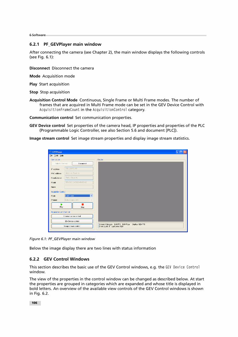
6 Software
6.2.1 PF_GEVPlayer main window
After connecting the camera (see Chapter 2), the main window displays the following controls(see Fig. 6.1):
Disconnect Disconnect the camera
Mode Acquisition mode
Play Start acquisition
Stop Stop acquisition
Acquisition Control Mode Continuous, Single Frame or Multi Frame modes. The number offrames that are acquired in Multi Frame mode can be set in the GEV Device Control withAcquisitionFrameCount in the AcquisitionControl category.
Communication control Set communication properties.
GEV Device control Set properties of the camera head, IP properties and properties of the PLC(Programmable Logic Controller, see also Section 5.6 and document [PLC]).
Image stream control Set image stream properties and display image stream statistics.
Figure 6.1: PF_GEVPlayer main window
Below the image display there are two lines with status information
6.2.2 GEV Control Windows
This section describes the basic use of the GEV Control windows, e.g. the GEV Device Controlwindow.
The view of the properties in the control window can be changed as described below. At startthe properties are grouped in categories which are expanded and whose title is displayed inbold letters. An overview of the available view controls of the GEV Control windows is shownin Fig. 6.2.
106

To have a quick overview of the available categories, all categories should be collapsed. Thecategories of interest can then be expanded again. If the name of the property is known, thenthe alphabetical view is convenient. If this is the first time that you use a Photonfocus GigEcamera, then the visibility should be left to Beginner.
The description of the currently selected property is shown at the bottom ot the window.
After selecting a property from a drop-down box it is necessary to press <Enter>or to click with the mouse on the control window to apply the property value tothe camera.
A red cross at the upper right corner of the GEV Control Window indicates aparameter error, i.e. a parameter is not correctly set. In this case you shouldcheck all properties. A red exclamation mark (!) at the right side of a parametervalue indicates that this parameters has to be set correctly.
T o g g l e c a t e g o r y /a l p h a b e t i c a l v i e w
E x p a n d a l lc a t e g o r i e s
C o l l a p s e a l lc a t e g o r i e s
V i s i b i l i t ys e l e c t i o n
E x p a n dc a t e g o r y
C o l l a p s ec a t e g o r y
P r o p e r t yd e s c r i p t i o n
P a r a m e t e re r r o r
i n d i c a t i o n
Figure 6.2: PF_GEVPlayer Control Window
.
6.2 PF_GEVPlayer 107

6 Software
6.2.3 Display Area
The images are displayed in the main window in the display area. A zoom menu is availablewhen right clicking in the display area. Another way to zoom is to press the Ctrl button whileusing the mouse wheel.
6.2.4 White Balance (Colour cameras only)
A white balance utility is available in the PF_GEVPlayer in Tools -> Image Filtering (see Fig.6.3). The gain of the colour channels can be adjusted manually by sliders or an auto whitebalance of the current image can be set by clicking on the White Balance button. To have acorrect white balance setting, the camera should be pointed to a neutral reference (object thatreflects all colours equally), e.g. a special grey reference card while clicking on the WhiteBalance button.
The white balance settings that were made as described in this section, are ap-plied by the PF_GEVPlayer software and are not stored in the camera. To storethe colour gain values in the camera, the Gain settings in the GEV Device Control(in AnalogControl) must be used. If the gain properties in the camera are used,then the PF_GEVPlayer RGB Filtering should be disabled.
Figure 6.3: PF_GEVPlayer image filtering dialog
6.2.5 Save camera setting to a file
The current camera settings can be saved to a file with the PF_GEVPlayer (File -> Save or SaveAs...). This file can later be applied to camera to restore the saved settings (File -> Open), Note,that the Device Control window must not be open to do this.
The MROI and LUT settings are not saved in the file.
108

6.2.6 Get feature list of camera
A list of all features of the Photonfocus G2 cameras in HTML format can be found in theGenICam_Feature_Lists sub-directory (in Start -> All Programs -> Photonfocus -> GigE_Tools).
Alternatively, the feature list of the connected camera can be retrieved with the PF_GEVPlayer(Tools -> Save Camera Features as HTML...).
6.3 Pleora SDK
The eBUS package provides the PureGEV C++ SDK for image acquisition and the setting ofproperties. A help file is installed in the Pleora installation directory, e.g. C:\ProgramFiles\Pleora Technologies Inc\eBUS SDK\Documentation.
Various code samples are installed in the installation directory, e.g. C:\Program Files\PleoraTechnologies Inc\eBUS SDK\Samples. The sample PvPipelineSample is recommended to start with.
Samples that show how to set device properties are included in the PFInstaller that can bedownloaded from the Photonfocus webpage.
6.4 Frequently used properties
A property list for every G2 camera is included in the PFInstaller that can be downloaded fromthe Photonfocus webpage.
The following list shows some frequently used properties that are available in the Beginnermode. The category name is given in parenthesis.
Width (ImageFormatControl) Width of the camera image ROI (region of interest)
Height (ImageFormatControl) Width of the camera image ROI
OffsetX, OffsetY (ImageFormatControl) Start of the camera image ROI
ExposureTime (AcquisitionControl) Exposure time in microseconds
TriggerMode (AcquisitionControl) External triggered mode
TriggerSource (AcquisitionControl) Trigger source if external triggered mode is selected
LinLog_Mode (LinLog) LinLog Mode
Header_Serial (Info / CameraInfo) Serial number of the camera
UserSetSave (UserSetControl) Saves the current camera settings to non-volatile flash memory.
6.3 Pleora SDK 109
6 Software
6.5 Calibration of the FPN Correction
The following procedures can be most easily done with the PF_GEVPlayer.
6.5.1 Offset Correction (CalibrateBlack)
The offset correction is based on a black reference image, which is taken at no illumination(e.g. lens aperture completely closed). The black reference image contains the fixed-patternnoise of the sensor, which can be subtracted from the live images in order to minimise thestatic noise.
Procedure to achieve a good correction:
1. Setup the camera width to the mode where it will be usually used. (Exposure time, ROI, ...)Due to the internal structure of the camera, best performance of calibration will beachieved when calibrating under "real conditions".
. If different ROI’s will be used, calibrate image under full ROI.
. If different exposure times will be used, calibrate the camera under the longestexposure time.
2. Set the following properties: Gain (in category AnalogControl) to 1, DigitalOffset (incategory AnalogControl) to 0, DigitalGain (in category DataOutput) to 1 andConvolver_3x3_0_Enable (in category Convolver) to 0. Due to the internal structure of thecamera these settings are required for correct calibration.
3. Wait until the camera has achieved working temperature.
4. Set the property Correction_Mode (in category Correction) to Off. This is not mandatory butrecommended.
5. Close the lens of the camera.
6. Check the value of the property Average_Value (in category PhotonfocusMain). Change theproperty BlackLevel (in category AnalogControl) until Average_Value is between 240 and 400DN. The property Average_Value can be updated by clicking on the propertyAverage_Update(in category PhotonfocusMain).
7. Click on CalibrateBlack (in category Calibration). Wait until the command has beenfinished, i.e.the property Correction_Busy (in category Calibration) is 0. Correction_Busy canbe updated by clicking on the property Correction_BusyUpdate (in category Calibration).
6.5.2 Gain Correction (CalibrateGrey)
The gain correction is based on a gray reference image, which is taken at uniform illuminationto give an image with a mid gray level. Gain correction is not a trivial feature. The quality ofthe gray reference image is crucial for proper gain correction.
The calibration of the gain correction can be skipped if gain correction will notbe used.
Procedure to achieve a good correction:
110

1. The procedure to calibrate the offset correction (see Section 6.5.1) must be run just beforecalibrating the gain correction.
Don’t turn off the camera between the calibration of the offset correction (Cali-brateBlack) and the calibration of the gain correction (CalibrateGrey).
2. Illuminate the camera homogeneously to produce a gray image with an Average_Value (incategory PhotonfocusMain) between 2200 and 3600 DN. Increase or decrease illumination ifAverage_Value is outside this range. The property Average_Value can be updated by clickingon the property Average_Update(in category PhotonfocusMain).
3. Click on CalibrateBlack (in category Calibration). Wait until the command has beenfinished, i.e.the property Correction_Busy (in category Calibration) is 0. Correction_Busy canbe updated by clicking on the property Correction_BusyUpdate (in category Calibration).
6.5.3 Storing the calibration in permanent memory
After running calibration procedures (see Section 6.5.1 and Section 6.5.2) the calibration valuesare stored in RAM. When the camera is turned off, their values are deleted.
To prevent this, the calibration values must be stored in flash memory. This can be done byclicking on the property Correction_SaveToFlash (in category Calibration). Wait until thecommand has been finished, i.e.the property Correction_Busy (in category Calibration) is 0.Correction_Busy can be updated by clicking on the property Correction_BusyUpdate (incategory Calibration).
6.6 Look-Up Table (LUT)
6.6.1 Overview
The LUT is described in detail in Section 4.8. All LUT settings can be set in the GUI(PF_GEVPlayer ). There are LUT setting examples in the PFInstaller, that can be downloadedfrom the Photonfocus webpage.
To manually set custom LUT values in the GUI is practically not feasable as up to4096 values for every LUT must set. This task should be done with the SDK.
If LUT values should be retained in the camera after disconnecting the power,then they must be saved with UserSetSave
6.6.2 Full ROI LUT
This section describe the settings for one LUT that is applied to the full ROI.
1. Set LUT_EnRegionLUT (in category RegionLUT) to False. This is required to use the full ROI LUT.
2. Set LUTEnable (in category LUTControl) to False. This is not mandatory but recommended.
3. Select LUT 0 by setting LUTSelector (in category LUTControl) to 0.
4. Set LUT content as described in Section 6.6.4.
5. Turn on LUT by setting LUTEnable to True.
6.6 Look-Up Table (LUT) 111

6 Software
6.6.3 Region LUT
The Region LUT feature is described in Section 4.8.4. Procedure to set the Region LUT:
1. Set LUT_EnRegionLUT (in category RegionLUT) to False. This is not mandatory butrecommended.
2. Set LUTEnable (in category LUTControl) to False. This is not mandatory but recommended.
3. Select LUT 0 by setting LUTSelector (in category LUTControl) to 0.
4. Set properties LUT_X, LUT_W, LUT_Y and LUT_H (all in category RegionLUT) to desiredvalue.
5. Set LUT content as described in Section 6.6.4.
6. If two Region LUT are required, then select LUT 1 by setting LUTSelector (in categoryLUTControl) to 1 and repeat steps 4 and 5.
7. Turn on LUT by setting LUTEnable to True.
8. Turn on Region LUT by setting LUT_EnRegionLUT (in category RegionLUT) to False.
6.6.4 User defined LUT settings
This section describes how to set user defined LUT values. It is assumed that the LUT wasselected as described in Section 6.6.2 or Section 6.6.3.
For every LUT value the following steps must be done:
1. Set LUTIndex (in category LUTControl) to desired value. The LUTIndex corresponds to thegrey value of the 12 bit input signal of the LUT.
2. Set LUTValue (in category LUTControl) to desired value. The LUTValue corresponds to thegrey value of the 8 bit output signal of the LUT.
The LUTIndex is auto incremented internally after setting a LUTValue. If consec-utive LUTIndex are written, then it is required to set LUTIndex only for the firstvalue. For the next values it is sufficient to set only the LUTValue.
6.6.5 Predefined LUT settings
Some predefined LUT are stored in the camera. To activate a predefined LUT:
1. Select LUT and RegionLUT (if required) as described in Section 6.6.2 and Section 6.6.3.
2. Set LUTAutoMode (in category LUTControl) to the desired value. The available settings aredescribed in property list of the camera which is contained in the PFInstaller.
3. If the LUTAutoMode requires additional settings (e.g. Gamma LUTAutoMode), then it can be setwith LUTAutoValue.
112

6.7 MROI
The MROI feature is described in Section 4.3.4. This section describes how to set the MROIvalues.
When MROI is enabled, then the camera internally processes the MROI entries sequentially,starting at MROI_Index 0. The processing is stopped when either the last MROI_Index is reached orwhen an entry with MROI_Y=1081 is reached.
Procedure to write MROI entries:
1. Disable MROI by setting MROI_Enable to False. This is mandatory otherwise setting theMROI entries will be ignored.
2. Set MROI_Index. In the first run it is set to 0 and then incremented in every run.
3. Set MROI_Y to the starting row of the MROI.
4. Set MROI_H to the height of the MROI.
5. Proceed with step 2, incrementing the MROI_Index. If no more MROI should be set, thenrun the steps 2 to 4 again (incrementing MROI_Index) but set MROI_Y to the value 1081.
6. Enable MROI by setting MROI_Enable to True.
7. Read the property MROI_Htot. Set the property Height (in category ImageFormatControl) tothe value of MROI_Htot. This is mandatory as this value is not automatically updated.
Example pseudo-code to set two MROI: The resulting total height of the example will be 400.
SetFeature(’MROI_Enable’, false);SetFeature(’MROI_Index’, 0);SetFeature(’MROI_Y’, 50);SetFeature(’MROI_H’, 100);SetFeature(’MROI_Index’, 1);SetFeature(’MROI_Y’, 600);SetFeature(’MROI_H’, 300);SetFeature(’MROI_Index’, 2);SetFeature(’MROI_Y’, 1081);SetFeature(’MROI_H’, 1);SetFeature(’MROI_Enable’, true);int heightTot;GetFeature(’MROI_Htot’, &heightTot);SetFeature(’Height’, heightTot);
6.8 Permanent Parameter Storage / Factory Reset
The property UserSetSave (in category UserSetControl) stores the current camera settings in thenon-volatile flash memory. At power-up these values are loaded.
The property UserSetSave (in category UserSetControl) overwrites the current camera settingswith the settings that are stored in the flash memory.
The command CameraHeadFactoryReset (in category PhotonfocusMain) restores the settings of thecamera head
The property CameraHeadStoreDefaults (in category PhotonfocusMain) stores onlythe settings of the camera head in the flash memory. It is recommended to useUserSetSave instead, as all properties are stored.
6.7 MROI 113

6 Software
The calibration values of the FPN calibration are not stored with UserSetSave (orCameraHeadStoreDefaults). Use the command Correction_SaveToFlash for this (seeCorrection_SaveToFlash).
6.9 Persistent IP address
It is possible to set a persistent IP address:
1. Set GevPersistentIPAddress (in category TransportLayerControl) to the desired IP address.
2. Set GevPersistentSubnetMask (in category TransportLayerControl) to the sub net mask.
3. Set GevCurrentIPConfigurationPersistent (in category TransportLayerControl) to True.
4. Set GevCurrentIPConfigurationDHCP (in category TransportLayerControl) to False.
5. The selected persistent IP address will be applied after a reboot of the camera.
6.10 PLC Settings
6.10.1 Introduction
The Programmable Logic Controller (PLC) is a powerful tool to generate triggers and softwareinterrupts. A functional diagram of the PLC tool is shown in Fig. 6.4. THE PLC tool is describedin detail with many examples in the [PLC] manual which is included in the PFInstaller.The simpliest application of the PLC is to connect a PLC input to a PLC output. The connectionof the ISO_IN0 input to the PLC_Q4 camera trigger is given as an example. The resultingconfiguration is shown in Section 6.10.2.
1. Identify the PLC notation of the desired input in Fig. 6.4. In our example, ISO_IN0 maps toA0 or Line0.
2. Select a Signal Routing Block (SRB) that has a connection to the desired PLC input andconnect it to the PLC input. In our example, SRB PLC_I0 will be used as it has a connectionto Line0. To connect the SRB to input, set PLC_I<x> to the input. In the example, set PLC_I0to Line0.
3. Identify the PLC notation of the desired output. A table of the PLC mapping is given inSection 5.6. In the example Q4 is the desired output.
4. Connect the LUT that corresponds to the desired output to the SRB from step 2. In theexample, PLC_Q4 is connected to PLC_I0. ISO_IN0 has an inverter in the I/O decouplingblock, therefore it is better to invert it again in the PLC: set PLC_Q4_Variable0 to PLC_I0_Not.Note that every LUT has the capability to connect up to 4 inputs. In the example only thefirst input (PLC_Q4_Variable0) is used. The other inputs are ignored by setting thePLC_Q4_Variable to Zero and the PLC_Q4_Operator to Or for inputs 1 to 3.
5. If a PLC output is used to connect to a camera trigger, then the corresponding TriggerSource must be activated. In the example, TriggerSource is set to PLC_Q4 and TriggerMode isset to On.
114

A 0 ( L i n e 0 )
A 1 ( L i n e 1 )S i g n a l
R o u t i n g
B l o c k
A 4
A 5
A 6
A 7
P L C7I S O _ I N 09
I S O _ I N 1
I S O _ I N C 0 _ P5
4I S O _ I N C 0 _ N
I S O _ I N C 1 _ P1 1
1 0I S O _ I N C 1 _ N
P o w e r C o n n e c t o r
I / O d e c o u p l i n g
F V A L
L V A L
D V A L
R E S E R V E D
P L C _ c t r l 0
P L C _ c t r l 1
P L C _ c t r l 2
P L C _ c t r l 3
Q 2
Q 3
Q 6
Q 7
p g 0 _ o u t
p g 1 _ o u t
p g 2 _ o u t
p g 3 _ o u t
d e l _ o u t
r s l _ o u t
g p _ c n t _ e q
g p _ c n t _ g t
t s _ t r i g 0
t s _ t r i g 1
t s _ t r i g 2
t s _ t r i g 3
L o o k u p
T a b l e
I 1
I 2
I 3
I 4
I 5
I 6
I 7
I 0
E n h a n c e d
F u n c t i o n
B l o c k
Q 0Q 1
Q 2
Q 3
Q 4
Q 5
Q 6
Q 7
Q 8
Q 9
Q 1 0
Q 1 1
Q 1 5
Q 1 6
Q 1 7
R e m o t e
C o n t r o l
B l o c kfrom
host PC
8
I S O _ O U T 1
I m a g e
C o n t r o l
B l o c k
Q 1 2
Q 1 3
Q 1 4
T r i g g e r S o f t w a r e
T r i g g e r S o u r c e
F r e e - r u n n i n g t r i g g e r
I n t e r n a l
c a m e r a
t r i g g e r
T r i g g e r M o d e
3I S O _ O U T 0S t r o b e
A 2 ( L i n e 2 )
A 3 ( L i n e 3 )
L i n e 1
P L C _ Q 4
S o f t w a r e
O f f
O n1C A M E R A _ G N D2C A M E R A _ P W R6I S O _ P W R1 2I S O _ G N D
I / O d e c o u p l i n g , i n v e r t i n g
T r i g g e r
D i v i d e r
Figure 6.4: PLC functional overview
6.10 PLC Settings 115

6 Software
6.10.2 PLC Settings for ISO_IN0 to PLC_Q4 Camera Trigger
This setting connects the ISO_IN0 to the internal camera trigger, see Table 6.1 (the visibility inthe PF_GEVPlayer must be set to Guru for this purpose).
Feature Value Category
TriggerMode On AcquisitionControl
TriggerSource PLC_Q4 AcquisitionControl
PLC_I0 Line0 <PLC>/SignalRoutingBlock
PLC_Q4_Variable0 PLC_I0_Not <PLC>/LookupTable/Q4
PLC_Q4_Operator0 Or <PLC>/LookupTable/Q4
PLC_Q4_Variable1 Zero <PLC>/LookupTable/Q4
PLC_Q4_Operator1 Or <PLC>/LookupTable/Q4
PLC_Q4_Variable2 Zero <PLC>/LookupTable/Q4
PLC_Q4_Operator2 Or <PLC>/LookupTable/Q4
PLC_Q4_Variable3 Zero <PLC>/LookupTable/Q4
Table 6.1: PLC Settings for ISO_IN0 to PLC_Q4 Camera Trigger (<PLC> = in categoryIPEngine/ProgrammableLogicController)
6.11 Miscellaneous Properties
6.11.1 DeviceTemperature
The property DeviceTemperature (in category DeviceControl) shows the value of the temperaturesensor that is selected by the property DeviceTemperatureSelector. It is updated every time theproperty DeviceTemperatureSelector is modified (see also note on drop-down boxes in Section6.2.2).
6.11.2 PixelFormat
The property PixelFormat (in category ImageFormatControl) sets the pixel format. For 10 bits and12 bits there is a selection of plain or packed format. The plain format uses more bandwidththan the packed format, but is easier to process in the software. Table 6.2 shows the number ofbits per pixel to are required for a pixel format. Fig. 6.5 shows the bit alignment of the packedpixel formats.
DataFormat Bits per pixel
Mono8 8
Mono10 16
Mono10Packed 10
Mono12 16
Mono12Packed 12
Table 6.2: GigE pixel format overview
116

The DR1 colour camera models have the BayerGB8 format. This should be used todisplay the debayered colour image in the PF_GEVPlayer display. To demodulatethe image by the SDK the format Mono8 must be used.
B y t e
B i t N r
P i x e l
9 8 7 6 5 4 3 2 - - 1 0 - - 1 0 9 8 7 6 5 4 3 2
0 1 2
P i x e l A P i x e l B P i x e l A P i x e l B
M o n o 1 0 P a c k e d
B y t e
B i t N r
P i x e l
1 1 1 0 9 8 7 6 5 4 3 2 1 0 3 2 1 0
0 1 2
P i x e l A P i x e l B P i x e l A P i x e l B
M o n o 1 2 P a c k e d
1 1 1 0 9 8 7 6 5 4
Figure 6.5: Packed Pixel Format
6.11.3 Colour Fine Gain (Colour cameras only)
To set the colour fine gain:
1. Set the GainSelector (in AnalogControl) to the desired position (see also below).
2. Set the Gain value to the desired value.
The GainSelector can have the following settings:
DigitalAll Overall gain applied to all colour channels
DigitalRed Gain applied to the red channel
DigitalGreen Gain applied to the green channel on the same row as the blue channel
DigitalBlue Gain applied to the blue channel
DigitalGreen2 Gain applied to the green channel on the same row as the red channel
To obtain colour gain values using the PF_GEVPlayer, follow could use the following procedure:
1. Open the camera in the PF_GEVPlayer, apply the desired settings and start the grabbing ofthe camera.
2. Set all colour gains of the camera (DigitalRed, DigitalGreen, DigitalBlue, DigitalGreen2) to1.
3. Point the camera to a neutral reference (object that reflects all colours equally), e.g. aspecial grey reference card.
4. Do a white balancing in the PF_GEVPlayer as described in Section 6.2.4.
5. Copy the values to the camera DigitalGain settings, i.e. copy the value of the Red channelin the Image Filtering window of the PF_GEVPlayer to the DigitalRed value value of thecamera (see above), copy the Green value to both DigitalGreen and DigitalGreen2 andcopy the Blue value to DigitalBlue. These values could also be stored in the camera’snon-volatile storage (see Section 6.8).
6. Disable RGB Filtering in the Image Filtering dialog of the PF_GEVPlayer as the colourchannel correction is now made in the camera.
6.11 Miscellaneous Properties 117

6 Software
6.12 Width setting in DR1 cameras
To set the width in DR1 cameras, please follow this procedure:
1. Set property Window_W to target width.
2. Read value of property WidthInterface.
3. Set property Width to the value of property WidthInterface.
When double rate is enabled (property DoubleRate_Enable=True), WidthInterface shows thewidth of the modulated image. When double rate is disabled (propertyDoubleRate_Enable=False), WidthInterface has the same value as Window_W.
6.13 Decoding of images in DR1 cameras
The images arrive in a encoded (compressed) format in the DR1 cameras if EnDoubleRate=True.There are functions in the pfDoubleRate package to decode the images. The packagedocumentation is located in the SDK\doc sub-directory of PFRemote installation directory.Examples are located in the SDK\Example\pfDoubleRate sub-directory. The package is installedwith the PFInstaller that can be downloaded from the Photonfocus web page. During theinstallation process, the option DR1 support must be checked.
There are separate decoding functions for monochrome and for colour DR1 cam-eras.
6.13.1 Status line in DR1 cameras
The newer revisions of the DR1 camera series contain the status line feature (see Section 4.11).The status line is supported in the pfDoubleRate.dll from the PFInstaller Rev. 2.38 and later.The whole image, including the status line, can be applied to the demodulation functions. Thestatus line is copied unmodified to the demodulated image, which is the correct behaviour asthe status line is never sent in modulated format.
6.14 DR1Evaluator
The DR1Evaluator is a tool to evaluate the effect of the encoding algorithm that isimplemented in the DR1 cameras. It is included in the PFInstaller that can be downloaded fromthe Photonfocus website.
The main window of the tool is shown in Fig. 6.6.An input file can be selected by clicking on the button Select Input File.
Suitable images for evaluation of the monochrome encoding algorithm can bedownloaded from the website http://www.imagecompression.info/test_images.Download the Gray 8 bit images. The best images for evaluation are the imagesthat were taken by a camera. The artificial images don’t reflect a "real-world"situation.
Only 8 bit monochrome images can be processed by the DR1 Evaluator tool.
118

Figure 6.6: DR1Evaluator
Only raw colour images, i.e. taken before debayering, can be used as input.
Optionally an output file can be selected by clicking on the button Select Output File. This isthe resulting file after modulation and demodulation of the input image.
Additionally a difference file can be generated by enabling the corresponding checkbox. Thevalue of every pixel is the absolute value of the difference InputFile-OutputFile.
The output images are produced by clicking on the Run button.
6.14 DR1Evaluator 119

6 Software
120
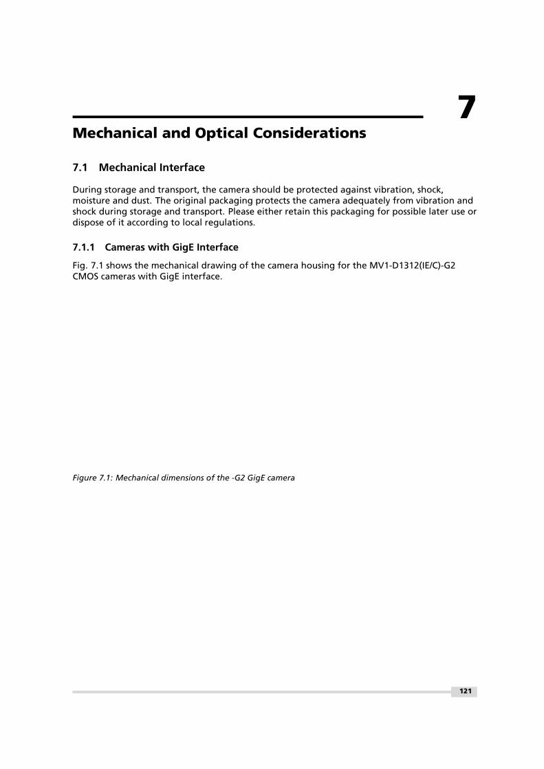
7Mechanical and Optical Considerations
7.1 Mechanical Interface
During storage and transport, the camera should be protected against vibration, shock,moisture and dust. The original packaging protects the camera adequately from vibration andshock during storage and transport. Please either retain this packaging for possible later use ordispose of it according to local regulations.
7.1.1 Cameras with GigE Interface
Fig. 7.1 shows the mechanical drawing of the camera housing for the MV1-D1312(IE/C)-G2CMOS cameras with GigE interface.
Figure 7.1: Mechanical dimensions of the -G2 GigE camera
121

7 Mechanical and Optical Considerations
7.2 Optical Interface
7.2.1 Cleaning the Sensor
The sensor is part of the optical path and should be handled like other optical components:with extreme care.
Dust can obscure pixels, producing dark patches in the images captured. Dust is most visiblewhen the illumination is collimated. Dark patches caused by dust or dirt shift position as theangle of illumination changes. Dust is normally not visible when the sensor is positioned at theexit port of an integrating sphere, where the illumination is diffuse.
1. The camera should only be cleaned in ESD-safe areas by ESD-trained personnel using wriststraps. Ideally, the sensor should be cleaned in a clean environment. Otherwise, in dustyenvironments, the sensor will immediately become dirty again after cleaning.
2. Use a high quality, low pressure air duster (e.g. Electrolube EAD400D, pure compressedinert gas, www.electrolube.com) to blow off loose particles. This step alone is usuallysufficient to clean the sensor of the most common contaminants.
Workshop air supply is not appropriate and may cause permanent damage tothe sensor.
3. If further cleaning is required, use a suitable lens wiper or Q-Tip moistened with anappropriate cleaning fluid to wipe the sensor surface as described below. Examples ofsuitable lens cleaning materials are given in Table 7.1. Cleaning materials must beESD-safe, lint-free and free from particles that may scratch the sensor surface.
Do not use ordinary cotton buds. These do not fulfil the above requirements andpermanent damage to the sensor may result.
4. Wipe the sensor carefully and slowly. First remove coarse particles and dirt from thesensor using Q-Tips soaked in 2-propanol, applying as little pressure as possible. Using amethod similar to that used for cleaning optical surfaces, clean the sensor by starting atany corner of the sensor and working towards the opposite corner. Finally, repeat theprocedure with methanol to remove streaks. It is imperative that no pressure be appliedto the surface of the sensor or to the black globe-top material (if present) surrounding theoptically active surface during the cleaning process.
122

Product Supplier Remark
EAD400D Airduster Electrolube, UK www.electrolube.com
Anticon Gold 9"x 9" Wiper Milliken, USA ESD safe and suitable forclass 100 environments.www.milliken.com
TX4025 Wiper Texwipe www.texwipe.com
Transplex Swab Texwipe
Small Q-Tips SWABSBB-003
Q-tips Hans J. Michael GmbH,Germany
www.hjm-reinraum.de
Large Q-Tips SWABSCA-003
Q-tips Hans J. Michael GmbH,Germany
Point Slim HUBY-340 Q-tips Hans J. Michael GmbH,Germany
Methanol Fluid Johnson Matthey GmbH,Germany
Semiconductor Grade99.9% min (Assay),Merck 12,6024, UN1230,slightly flammable andpoisonous.www.alfa-chemcat.com
2-Propanol(Iso-Propanol)
Fluid Johnson Matthey GmbH,Germany
Semiconductor Grade99.5% min (Assay) Merck12,5227, UN1219,slightly flammable.www.alfa-chemcat.com
Table 7.1: Recommended materials for sensor cleaning
For cleaning the sensor, Photonfocus recommends the products available from the suppliers aslisted in Table 7.1.
. Cleaning tools (except chemicals) can be purchased directly from Photonfocus(www.photonfocus.com).
.
7.2 Optical Interface 123

7 Mechanical and Optical Considerations
7.3 Compliance
C E C o m p l i a n c e S t a t e m e n t
W e ,
P h o t o n f o c u s A G ,
C H - 8 8 5 3 L a c h e n , S w i t z e r l a n d
d e c l a r e u n d e r o u r s o l e r e s p o n s i b i l i t y t h a t t h e f o l l o w i n g p r o d u c t s
M V - D 1 0 2 4 - 2 8 - C L - 1 0 , M V - D 1 0 2 4 - 8 0 - C L - 8 , M V - D 1 0 2 4 - 1 6 0 - C L - 8
M V - D 7 5 2 - 2 8 - C L - 1 0 , M V - D 7 5 2 - 8 0 - C L - 8 , M V - D 7 5 2 - 1 6 0 - C L - 8
M V - D 6 4 0 - 3 3 - C L - 1 0 , M V - D 6 4 0 - 6 6 - C L - 1 0 , M V - D 6 4 0 - 4 8 - U 2 - 8M V - D 6 4 0 C - 3 3 - C L - 1 0 , M V - D 6 4 0 C - 6 6 - C L - 1 0 , M V - D 6 4 0 C - 4 8 - U 2 - 8
M V - D 1 0 2 4 E - 4 0 , M V - D 7 5 2 E - 4 0 , M V - D 7 5 0 E - 2 0 ( C a m e r a L i n k a n dU S B 2 . 0 M o d e l s ) , M V - D 1 0 2 4 E - 8 0 , M V - D 1 0 2 4 E - 1 6 0
M V - D 1 0 2 4 E - 3 D 0 1 - 1 6 0
M V 2 - D 1 2 8 0 - 6 4 0 - C L - 8
S M 2 - D 1 0 2 4 - 8 0 / V i s i o n C a m P S
D S 1 - D 1 0 2 4 - 4 0 - C L , D S 1 - D 1 0 2 4 - 4 0 - U 2 ,D S 1 - D 1 0 2 4 - 8 0 - C L , D S 1 - D 1 0 2 4 - 1 6 0 - C L
D S 1 - D 1 3 1 2 - 1 6 0 - C L M V 1 - D 1 3 1 2 ( I E ) - 4 0 - C L , M V 1 - D 1 3 1 2 ( I E ) - 8 0 - C L , M V 1 - D 1 3 1 2 ( I E ) - 1 6 0 - C L ,M V 1 - D 1 3 1 2 ( I E ) - 2 4 0 - C L , E L 1 - D 1 3 1 2 - 1 6 0 - C LM V 1 - D 1 3 1 2 ( I E ) - G 2 S e r i e s , D R 1 - D 1 3 1 2 ( I E ) - 2 0 0 - G 2 - 8
M V 1 - D 2 0 8 0 ( I E ) - C L S e r i e s
D i g i p e a t e r C L B 2 6
a r e i n c o m p l i a n c e w i t h t h e b e l o w m e n t i o n e d s t a n d a r d s a c c o r d i n g t o
t h e p r o v i s i o n s o f E u r o p e a n S t a n d a r d s D i r e c t i v e s :
E N 6 1 0 0 0 - 6 - 3 : 2 0 0 1
E N 6 1 0 0 0 - 6 - 2 : 2 0 0 1
E N 6 1 0 0 0 - 4 - 6 : 1 9 9 6
E N 6 1 0 0 0 - 4 - 4 : 1 9 9 6
E N 6 1 0 0 0 - 4 - 3 : 1 9 9 6
E N 6 1 0 0 0 - 4 - 2 : 1 9 9 5
E N 5 5 0 2 2 : 1 9 9 4
P h o t o n f o c u s A G , O c t o b e r 2 0 1 1
Figure 7.2: CE Compliance Statement
124

8Warranty
The manufacturer alone reserves the right to recognize warranty claims.
8.1 Warranty Terms
The manufacturer warrants to distributor and end customer that for a period of two yearsfrom the date of the shipment from manufacturer or distributor to end customer (the"Warranty Period") that:
• the product will substantially conform to the specifications set forth in the applicabledocumentation published by the manufacturer and accompanying said product, and
• the product shall be free from defects in materials and workmanship under normal use.
The distributor shall not make or pass on to any party any warranty or representation onbehalf of the manufacturer other than or inconsistent with the above limited warranty set.
8.2 Warranty Claim
The above warranty does not apply to any product that has been modified or al-tered by any party other than manufacturer, or for any defects caused by any useof the product in a manner for which it was not designed, or by the negligenceof any party other than manufacturer.
125

8 Warranty
126

9References
All referenced documents can be downloaded from our website at www.photonfocus.com.
AN001 Application Note "LinLog", Photonfocus, December 2002
AN007 Application Note "Camera Acquisition Modes", Photonfocus, March 2004
AN008 Application Note "Photometry versus Radiometry", Photonfocus, December 2004
AN026 Application Note "LFSR Test Images", Photonfocus, September 2005
AN030 Application Note "LinLog® Parameter Optimization Strategies", February 2009
GEVQS GEVPlayer Quick Start Guide, Pleora Technologies. Included in eBUS installer.
MAN051 Manual "Photonfocus GigE Quick Start Guide", Photonfocus
PLC iPORT Programmable Logic Controller Reference Guide, Pleora Technologies. Included inGigE software package.
127

9 References
128

APinouts
A.1 Power Supply Connector
The power supply connectors are available from Hirose connectors atwww.hirose-connectors.com. Fig. A.1 shows the power supply plug from the solder side. Thepin assignment of the power supply plug is given in Table A.2.
It is extremely important that you apply the appropriate voltages to your camera.Incorrect voltages will damage or destroy the camera.
The connection of the input and output signals is described in Section 5.5.
A suitable power supply can be ordered from your Photonfocus dealership.
Connector Type Order Nr.
12-pole Hirose HR10A-10P-12S soldering 110-0402-0
12-pole Hirose HR10A-10P-12SC crimping 110-0604-4
Table A.1: Power supply connectors (Hirose HR10 series, female connector)
91
1 21 1
1 0 8
7
65
4
3
2
Figure A.1: Power supply connector, 12-pole female (rear view of connector, solder side)
129

A Pinouts
Pin I/O Type Name Description
1 PWR CAMERA_GND Camera GND, 0V
2 PWR CAMERA_PWR Camera Power 12V..24V
3 O ISO_OUT0 Default Strobe out, internally Pulled up to ISO_PWRwith 4k7 Resistor
4 I ISO_INC0_N INC0 differential RS-422 input, negative polarity
5 I ISO_INC0_P INC0 differential RS-422 input, positive polarity
6 PWR ISO_PWR Power supply 5V..24V for output signals; Do NOTconnect to camera Power
7 I ISO_IN0 IN0 input signal
8 O ISO_OUT1 (MISC) Q1 output from PLC, no Pull up to ISO_PWR ; can beused as additional output (by adding Pull up) or ascontrollable switch (max. 100mA, no capacitive orinductive load)
9 I ISO_IN1(Trigger IN) Default Trigger IN
10 I ISO_INC1_N INC1 differential RS-422 input, negative polarity
11 I ISO_INC1_P INC1 differential RS-422 input, positive polarity
12 PWR ISO_GND I/O GND, 0V
Table A.2: Power supply connector pin assignment
130

BRevision History
Revision Date Changes
1.0 October 2011 First version
1.1 November 2011 Chapter "How to get started (GigE G2)" reordered.
Chapter "Product Specification": camera size corrected.
Section TriggerSource adapted to GenICam specification.
Section Trigger and AcquisitionMode added.
Appendix "Power Supply Connector": wrong connector typeindicated in table (male instead of female).
Section "PLC connections": correction: Q0 is not connected topower connector, ISO_OUT1 is on Q1.
Chapter "Software": sections "DR1_GEVPlayer" and "Imagedemodulation" added.
1.2 April 2012 Chapter "How to get started (GigE G2)", section "HardwareInstallation": description of NIC requirement slightly modified.
Chapter "Software": section about PLC added.
Appendix "Power Supply Connector": description of pin 8slightly modified. Pin out diagram corrected.
1.3 May 2012 Colour models added
Adapted to PFInstaller_2_30 and later
1.4 May 2014 Section "Power and Ground Connection for GigE G2Cameras": removed warning about connecting ISO_GND /ISO_PWR and camera ground / power.
131