ufs 3.0 - controller design considerations 3.0 controller challenges flash memory summit 2017 santa...
TRANSCRIPT
UFS 3.0 -Controller Design Considerations
Phison Electronics Corp.
Strategic Account Manager
Keith Tsai
1Flash Memory Summit 2017Santa Clara, CA

Before I Start….
1. What’s the benefit of adopting UFS?
2. What’s the UFS application/market?
What’s the UFS3.0 requirements that controller company need to consider?

Mobile Storage Evolution
3
eMMC
• Latest widely adopted standard before UFS 2.x
• Limited to 400MB/s (duplex) since 2013
UFS 1.x• Not adopted
UFS 2.x
• Offers desktop-grade performance of ~1200MB/s over full-duplex links
• Good adoption in flagship devices (2017)
UFS 3.0
• Doubles UFS 2.x performance, offering ~2400MB/s
• Requirements are tough for mobile form factors
Flash Memory Summit 2017Santa Clara, CA

1. High Throughput
2. Low Active Power
3. Low Latencies
4. Cost Management
a) Reduced DIE Size
b) Support to latest 3D NAND technologies
UFS 3.0 Controller Requirements
Flash Memory Summit 2017Santa Clara, CA

1. High Throughput
2. Low Active Power
3. Low Latencies
4. Cost Management
a) Reduced DIE Size
b) Support to latest 3D NAND technologies
UFS 3.0 Controller Requirements
Flash Memory Summit 2017Santa Clara, CA
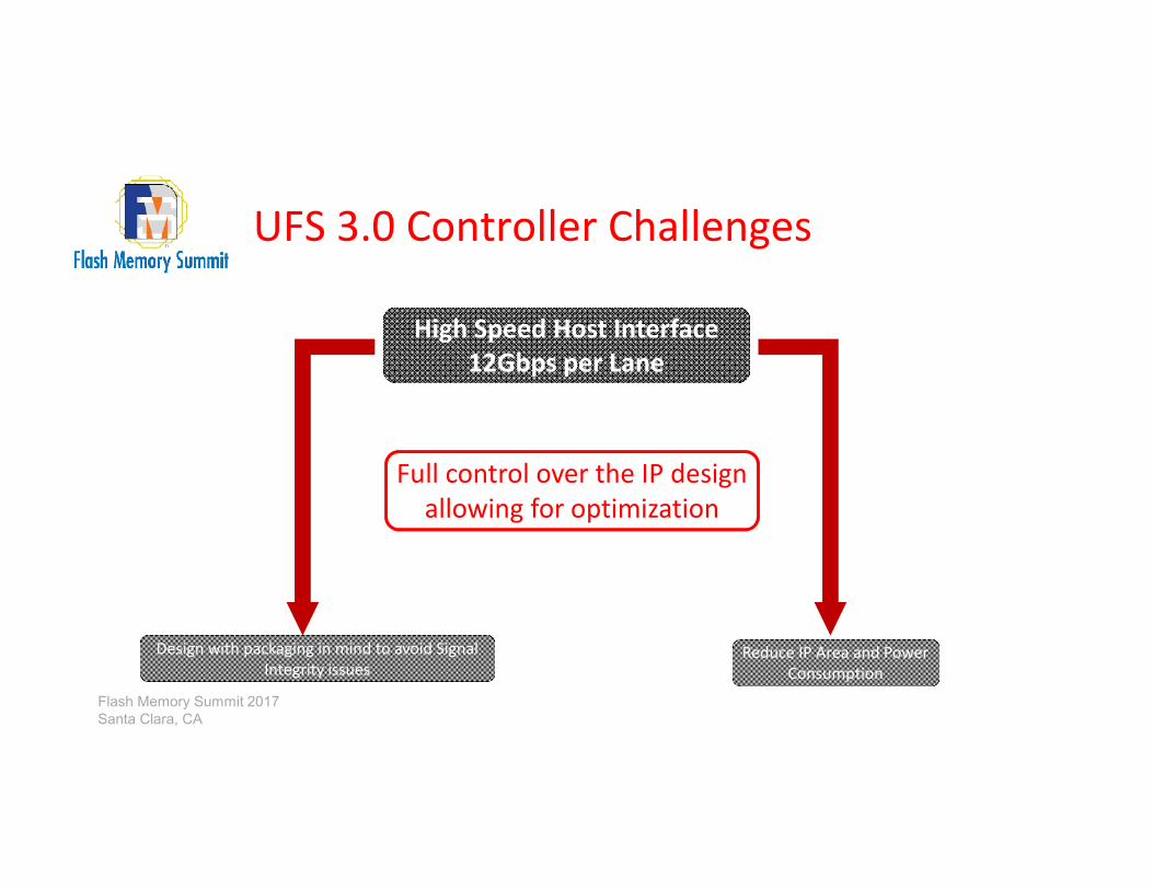
Full control over the IP design allowing for optimization
Design with packaging in mind to avoid Signal Integrity issues
Reduce IP Area and Power Consumption
High Speed Host Interface12Gbps per Lane
UFS 3.0 Controller Challenges
Flash Memory Summit 2017Santa Clara, CA

1. High Throughput
2. Low Active Power
3. Low Latencies
4. Cost Management
a) Reduced DIE Size
b) Support to latest 3D NAND technologies
UFS 3.0 Controller Requirements
Flash Memory Summit 2017Santa Clara, CA

High SpeedError Correction Engine
Hardware Acceleration to reduce FW & CPU Overhead
High SpeedFlash Interface
LOWLatencies
QoS (Quality of Service)
UFS 3.0 Controller Challenges
Having in-house IPs can shape the design around these requirements
Flash Memory Summit 2017Santa Clara, CA

1. High Throughput
2. Low Active Power
3. Low Latencies
4. Cost Management
a) Reduced DIE Size
b) Support to latest 3D NAND technologies
UFS 3.0 Controller Requirements
Flash Memory Summit 2017Santa Clara, CA
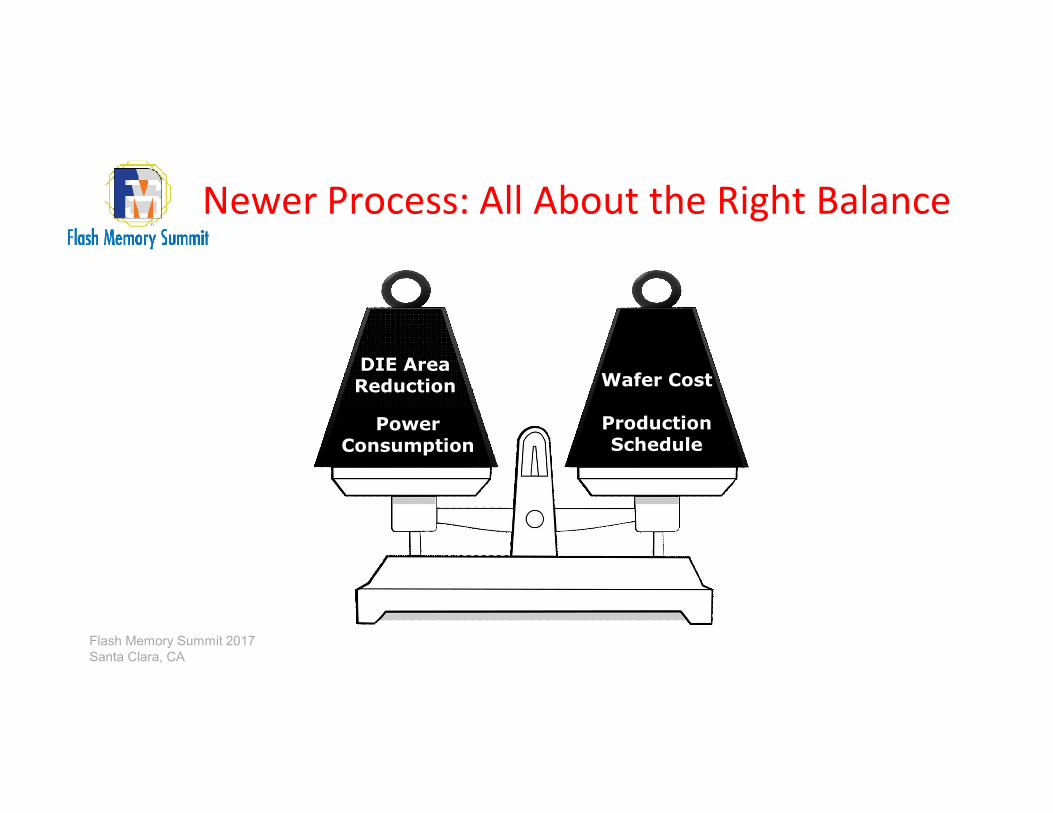
Wafer Cost
ProductionSchedule
Power Consumption
DIE AreaReduction
Newer Process: All About the Right Balance
Flash Memory Summit 2017Santa Clara, CA

EXAMPLE – Phison’s Error Correction Engine IP StudyPhison Gen1 Phison Gen2 Next Gen
Application UFS 2.1 - HS G3 x1-L UFS 2.1 - HS G3 x2-L UFS3.0 - HS G4 x2-L
ECC Throughput (Higher than I/F)
800MB/s(800 x1)
1333MB/s(800 x1.66)
2666MB/s(800 x3.33)
Area (aprox.) x1 x0.32 x0.44
Power Consumption x1 x0.46 x0.67
DIE Area Cost x1 x0.53 x0.75
A newer process will bring more advantages. However mask investment, wafer cost, production schedule, IP availability (if not in-house) will have to be considered
Choosing the Ideal Process
Flash Memory Summit 2017Santa Clara, CA

In device controller design, the balance between performance,
power and cost is critical. A total control of the design will offer
more flexibility to optimize the solution
Summary
Flash Memory Summit 2017Santa Clara, CA
In-house IPs can optimize the cost and requirements
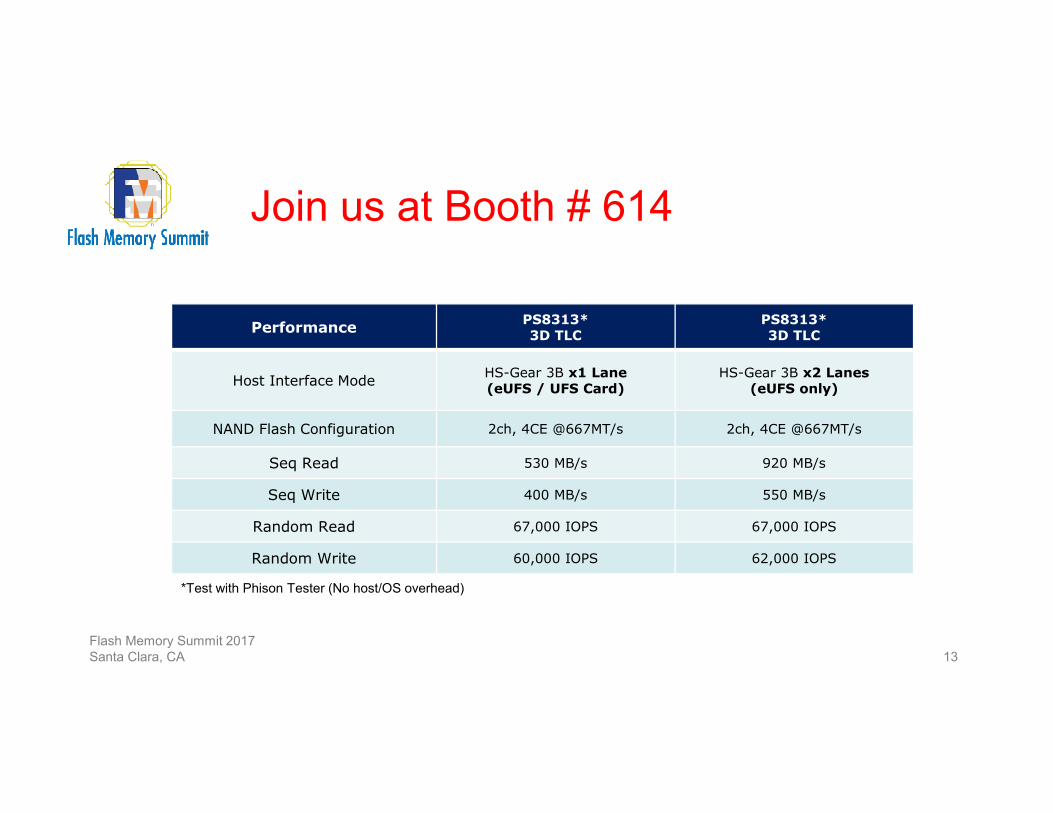
Join us at Booth # 614
PerformancePS8313*3D TLC
PS8313*3D TLC
Host Interface ModeHS-Gear 3B x1 Lane(eUFS / UFS Card)
HS-Gear 3B x2 Lanes(eUFS only)
NAND Flash Configuration 2ch, 4CE @667MT/s 2ch, 4CE @667MT/s
Seq Read 530 MB/s 920 MB/s
Seq Write 400 MB/s 550 MB/s
Random Read 67,000 IOPS 67,000 IOPS
Random Write 60,000 IOPS 62,000 IOPS
Flash Memory Summit 2017Santa Clara, CA 13
*Test with Phison Tester (No host/OS overhead)

Thank you
Flash Memory Summit 2017Santa Clara, CA 14