ultracompact high-efficiency polarising beam splitter
TRANSCRIPT
Ultracompact high-efficiency polarising beam splitter based on silicon nanobrick arrays
Guoxing Zheng,1,2,* Guogen Liu,1 Mitchell Guy Kenney,3 Zile Li,1 Ping’an He,1 Song Li,1,2 Zhi Ren,4 and Qiling Deng5
1Electronic Information School, Wuhan University, Wuhan, 430072, China 2Cooperative Innovation Center of Geospatial Technology, Wuhan University, Wuhan, 430079, China
3School of Engineering, University of Glasgow, Glasgow, G12 8LT, UK 4School of Mathematics and Physics, North China Electric Power University, Baoding 071003, China
5Institute of Optics & Electronics, Chinese Academy of Sciences, Chengdu, 610209, China *[email protected]
Abstract: Since the transmission of anisotropic nano-structures is sensitive to the polarisation of an incident beam, a novel polarising beam splitter (PBS) based on silicon nanobrick arrays is proposed. With careful design of such structures, an incident beam with polarisation direction aligned with the long axis of the nanobrick is almost totally reflected (~98.5%), whilst that along the short axis is nearly totally transmitted (~94.3%). More importantly, by simply changing the width of the nanobrick we can shift the peak response wavelength from 1460 nm to 1625 nm, covering S, C and L bands of the fiber telecommunications windows. The silicon nanobrick-based PBS can find applications in many fields which require ultracompactness, high efficiency, and compatibility with semiconductor industry technologies.
©2016 Optical Society of America
OCIS codes: (050.6624) Subwavelength structures; (230.3990) Micro-optical devices; (240.0240) Optics at surfaces.
References and links 1. L. Zhou and W. Liu, “Broadband polarizing beam splitter with an embedded metal-wire nanograting,” Opt. Lett.
30(12), 1434–1436 (2005).2. H. Lajunen, J. Turunen, and J. Tervo, “Design of polarization gratings for broadband illumination,” Opt. Express
13(8), 3055–3067 (2005).3. R. Schnabel, A. Bunkowski, O. Burmeister, and K. Danzmann, “Three-port beam splitters-combiners for
interferometer applications,” Opt. Lett. 31(5), 658–660 (2006).4. Z. Wu, P. E. Powers, A. M. Sarangan, and Q. Zhan, “Optical characterization of wiregrid micropolarizers
designed for infrared imaging polarimetry,” Opt. Lett. 33(15), 1653–1655 (2008).5. M. Xu, H. Urbach, D. de Boer, and H. Cornelissen, “Wire-grid diffraction gratings used as polarizing beam
splitter for visible light and applied in liquid crystal on silicon,” Opt. Express 13(7), 2303–2320 (2005).6. C. R. A. Lima, L. L. Soares, L. Cescato, and A. L. Gobbi, “Reflecting polarizing beam splitter,” Opt. Lett. 22(4),
203–205 (1997). 7. P. Lalanne, J. Hazart, P. Chavel, E. Cambril, and H. Launois, “A transmission polarizing beam splitter grating,”
Pure Appl. Opt. 1(2), 215–219 (1999).8. Y. Ekinci, H. H. Solak, C. David, and H. Sigg, “Bilayer Al wire-grids as broadband and high-performance
polarizers,” Opt. Express 14(6), 2323–2334 (2006).9. J. Wu, C. Zhou, H. Cao, and A. Hu, “Broadband polarizing beam splitter with metal-wire nanograting in near
infrared region,” Opt. Laser Technol. 47, 166–170 (2013).10. D. Yi, Y. Yan, H. Liu, S. Lu, and G. Jin, “Broadband polarizing beam splitter based on the form birefringence of
a subwavelength grating in the quasi-static domain,” Opt. Lett. 29(7), 754–756 (2004).11. J. Zheng, C. Zhou, J. Feng, and B. Wang, “Polarizing beam splitter of deep-etched triangular-groove fused-silica
gratings,” Opt. Lett. 33(14), 1554–1556 (2008).12. J. Feng, C. Zhou, H. Cao, and P. Lv, “Deep-etched sinusoidal polarizing beam splitter grating,” Appl. Opt.
49(10), 1739–1743 (2010).13. H. Wu, W. Mo, J. Hou, D. Gao, R. Hao, R. Guo, W. Wu, and Z. Zhou, “Polarizing beam splitter based on a
subwavelength asymmetric profile grating,” J. Opt. 12(1), 015703 (2010).14. B. Wang, L. Lei, L. Chen, and J. Zhou, “Connecting-layer-based polarizing beam splitter grating with high
efficiency for both TE and TM polarizations,” Opt. Laser Technol. 44(7), 2145–2148 (2012).15. B. Wang, L. Chen, L. Lei, and J. Zhou, “Two-layer dielectric grating for polarization-selective beam splitter with
improved efficiency and bandwidth,” Opt. Commun. 294, 329–332 (2013).
#258366 Received 28 Jan 2016; revised 11 Mar 2016; accepted 15 Mar 2016; published 18 Mar 2016 © 2016 OSA 21 Mar 2016 | Vol. 24, No. 6 | DOI:10.1364/OE.24.006749 | OPTICS EXPRESS 6749
16. Z. Lu, Y. Tang, Y. Shen, X. Liu, and J. Zi, “Polarization beam splitting in two-dimensional photonic crystals based on negative refraction,” Phys. Lett. A 346(1-3), 243–247 (2005).
17. X. Ao and S. He, “Polarization beam splitters based on a two-dimensional photonic crystal of negative refraction,” Opt. Lett. 30(16), 2152–2154 (2005).
18. Y. Zhang, Y. Jiang, W. Xue, and S. He, “A broad-angle polarization beam splitter based on a simple dielectric periodic structure,” Opt. Express 15(22), 14363–14368 (2007).
19. E. Schonbrun, Q. Wu, W. Park, T. Yamashita, and C. J. Summers, “Polarization beam splitter based on a photonic crystal heterostructure,” Opt. Lett. 31(21), 3104–3106 (2006).
20. S. Y. Lee, K. Kim, G. Y. Lee, and B. Lee, “Polarization-multiplexed plasmonic phase generation with distributed nanoslits,” Opt. Express 23(12), 15598–15607 (2015).
21. S. Zhang, C. Gu, and H. Xu, “Single nanoparticle couplers for plasmonic waveguides,” Small 10(21), 4264–4269 (2014).
22. Z. L. Deng, S. Zhang, and G. P. Wang, “A facile grating approach towards broadband, wide-angle and high-efficiency holographic metasurfaces,” Nanoscale 8(3), 1588–1594 (2016).
23. L. Du, S. S. Kou, E. Balaur, J. J. Cadusch, A. Roberts, B. Abbey, X. C. Yuan, D. Tang, and J. Lin, “Broadbandchirality-coded meta-aperture for photon-spin resolving,” Nat. Commun. 6, 10051 (2015).
24. Y. Wang, M. Pu, Z. Zhang, X. Li, X. Ma, Z. Zhao, and X. Luo, “Quasi-continuous metasurface for ultra-broadband and polarization-controlled electromagnetic beam deflection,” Sci. Rep. 5, 17733 (2015).
25. N. Yu, P. Genevet, M. A. Kats, F. Aieta, J. P. Tetienne, F. Capasso, and Z. Gaburro, “Light propagation withphase discontinuities: generalized laws of reflection and refraction,” Science 334(6054), 333–337 (2011).
26. X. Chen, L. Huang, H. Mühlenbernd, G. Li, B. Bai, Q. Tan, G. Jin, C. W. Qiu, S. Zhang, and T. Zentgraf, “Dual-polarity plasmonic metalens for visible light,” Nat. Commun. 3, 1198 (2012).
27. L. Huang, X. Chen, H. Mühlenbernd, H. Zhang, S. Chen, B. Bai, Q. Tan, G. Jin, K. Cheah, C. Qiu, J. Li, T. Zentgraf, and S. Zhang, “Three-dimensional optical holography using a plasmonic metasurface,” Nat. Commum.4, 2808 (2013).
28. D. Wen, F. Yue, G. Li, G. Zheng, K. Chan, S. Chen, M. Chen, K. F. Li, P. W. Wong, K. W. Cheah, E. Y. Pun, S. Zhang, and X. Chen, “Helicity multiplexed broadband metasurface holograms,” Nat. Commun. 6, 8241 (2015).
29. G. Zheng, H. Mühlenbernd, M. Kenney, G. Li, T. Zentgraf, and S. Zhang, “Metasurface holograms reaching 80% efficiency,” Nat. Nanotechnol. 10(4), 308–312 (2015).
30. Z. Li, G. Zheng, P. He, S. Li, Q. Deng, J. Zhao, and Y. Ai, “All-silicon nanorod-based Dammann gratings,” Opt. Lett. 40(18), 4285–4288 (2015).
31. E. Schonbrun, K. Seo, and K. B. Crozier, “Reconfigurable imaging systems using elliptical nanowires,” Nano Lett. 11(10), 4299–4303 (2011).
32. V. Gruev, R. Perkins, and T. York, “CCD polarization imaging sensor with aluminum nanowire optical filters,”Opt. Express 18(18), 19087–19094 (2010).
33. N. J. Brock, B. T. Kimbrough, and J. E. Millerd, “A pixelated micropolarizer-based camera for instantaneous interferometric measurements,” Proc. SPIE 8160, 81600W (2011).
1. Introduction
The polarising beam splitter (PBS), which can split an arbitrarily polarised incident beam into two orthogonally polarised beams, has a wide range of applications such as optical fiber telecommunications, magneto-optic data storage, imaging systems and many other potential fields [1–5]. Since a PBS is always integrated into a multifunctional optoelectronic device in photonic integrated circuits (PICs), a compact PBS is beneficial; suffering from their bulky volume and heavy weight, a conventional PBS (birefringent crystal prism or 45° right-angle prism with multilayer thin film) is cumbersome and would hinder the integration for PICs applications. Due to the recent developments of grating vector theory and microfabrication, subwavelength gratings which function as a PBS attract much attention. Many approaches of grating-based PBS’s have been presented, including simple binary reflection [6] or transmission [7], metal nanowire [8,9], sandwiched structure [10], triangular [11] or sinusoidal grooves [12], asymmetric profile [13], connecting layer [14] and two-layer dielectric gratings [15]. The grating-based PBS features advantages such as their small size, high efficiency and large extinction ratio. However, some of them have complicated structures; of these, some would drive the diffractive beams into non-normal angles, which would bring inconvenience for many applications. One other way to realise a compact PBS is using photonic crystals (PCs). The PC-based PBS has two different categories: One method is taking advantage of the difference between the dispersion characteristics of transverse electronic (TE) and transverse magnetic (TM) modes, which would make the refractive index of the photonic crystal be positive for one polarisation mode but negative for the other [16–18]; another way is through the use of the photonic band gap, with which one can put a polarisation mode in the forbidden band and the other in the conduction band to separate two
#258366 Received 28 Jan 2016; revised 11 Mar 2016; accepted 15 Mar 2016; published 18 Mar 2016 © 2016 OSA 21 Mar 2016 | Vol. 24, No. 6 | DOI:10.1364/OE.24.006749 | OPTICS EXPRESS 6750
polarised modes [19]. The PC-based PBS exhibits many advantages, such as small size, large angle separation and high efficiency, but despite this the fabrication is complicated and it cannot meet the requirements for mass production to date.
The rapid development of metasurfaces (or two-dimensional (2D) metamaterials) brings to the table innovation for conventional optical elements. Metamaterials are a kind of composite material which is artificially designed to exhibit unconventional optical properties that natural materials do not possess [20–31]. Recently, many literatures state that arbitrary and accurate phase control can be achieved by using metasurfaces [25–29]. Some new reports indicate that particularly high efficiency has been achieved with the utilisation of metasurfaces [28,29]. Owing to their tiny size and planar structure, metasurfaces are very easy to be integrated with many other functional optoelectronic elements. Furthermore, the fabrication of metasurfaces is compatible with the conventional lithography technique (and only one-step lithography is required), which make them very suitable for mass production. The drawbacks of present PBS devices may be overcome and some unique features are expected if one employs metasurfaces for such application.
In our previous works, we proved that silicon nanorods (or nanobricks) can be used to control the phase of the incident beam accurately [30]. In this paper, we apply these previous developments and verify both by analysis and simulation that silicon nanobrick arrays sitting on a glass substrate can act as a high efficiency micro-PBS. These carefully designed thin nanobrick arrays, characterised by periodic nanostructures with identical cell dimensions, can separate the incident beams into two orthogonal polarisation states with high efficiencies (both for transmission and reflection) whilst maintaining a normally transmitted propagation direction i.e. no refraction into non-normal angles. The ultracompact and high efficiency micro-PBS presented here may find its benefit in many fields such as for photonic integrated circuits.
2. Working principles
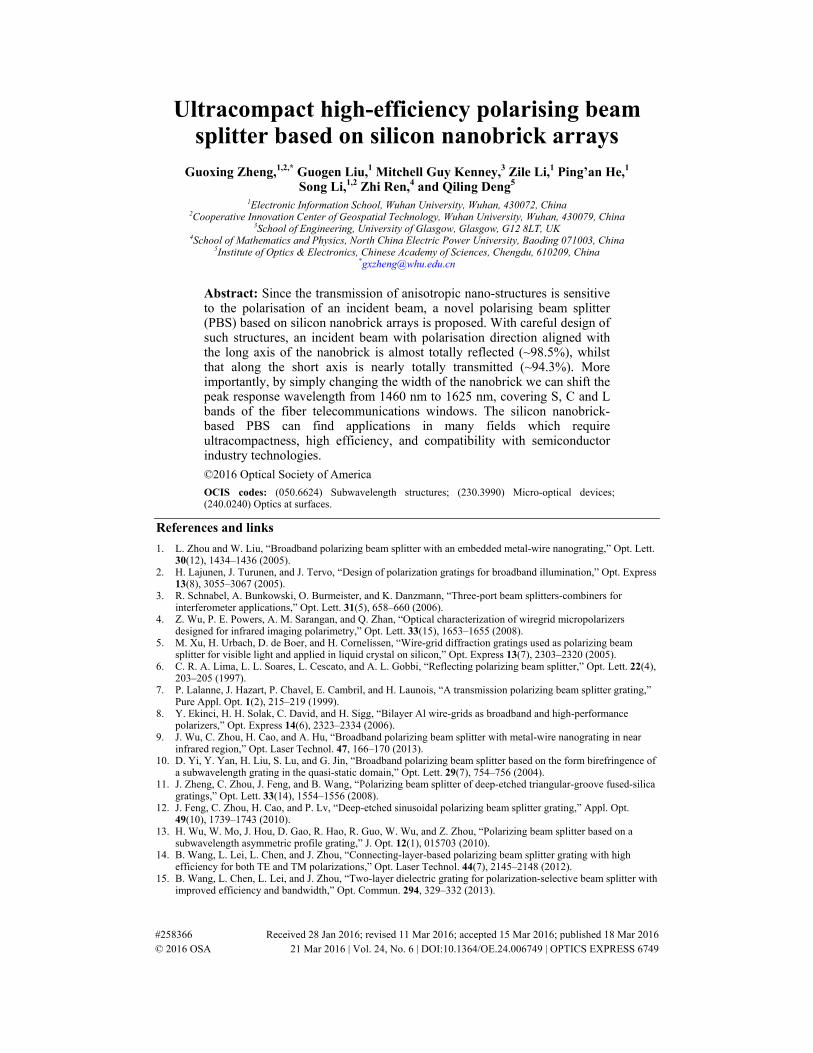
Fig. 1. Illustration of PBS based on silicon nanobrick arrays sitting on a glass substrate. All the nanobricks have the same dimensions and orientations. Incident beams with polarisation direction along the long axis of the nanobrick are reflected and those with polarisation direction along the short axis are transmitted. This dielectric device works in the fiber telecommunications windows (~1550 nm).
A schematic diagram of the PBS based on silicon (refractive index n≈3.67) nanobrick arrays is shown in Fig. 1, whereby periodic nanobricks with length L, width W, height H and cell
#258366 Received 28 Jan 2016; revised 11 Mar 2016; accepted 15 Mar 2016; published 18 Mar 2016 © 2016 OSA 21 Mar 2016 | Vol. 24, No. 6 | DOI:10.1364/OE.24.006749 | OPTICS EXPRESS 6751
size C sit on a glass (refractive index ns≈1.51) substrate. Due to the nanobrick’s size difference between the long and short axes (as illustrated in Fig. 1), the electromagnetic responses along each nanobrick axis becomes different, which is equivalent to form birefringence. Since nanobricks can be considered as waveguides [31], the mode transmitive indices of such a waveguide would be different in two orthogonal directions and an impinging beam composed of different polarisation states would experience different phase delays for each state. On the other hand, an impedance mismatch occurs at the two ends of the nanobrick along the propagation direction (from air to silicon at one end and from silicon to glass substrate at the other end); as a result, resonance would occur when beams propagate back and forth in the nanobrick waveguide. By carefully choosing the dimension parameters of the nanobrick and operation wavelength, the beams with polarisation direction along the long axis of the nanobrick would be (ideally) totally reflected, whilst the orthogonal polarisation would be (ideally) totally transmitted. Therefore, the normally incident beams can be divided into reflective and refractive parts according to their polarisation states after they impinge on the PBS. This forms the basic principle of a nanobrick-based micro-PBS.
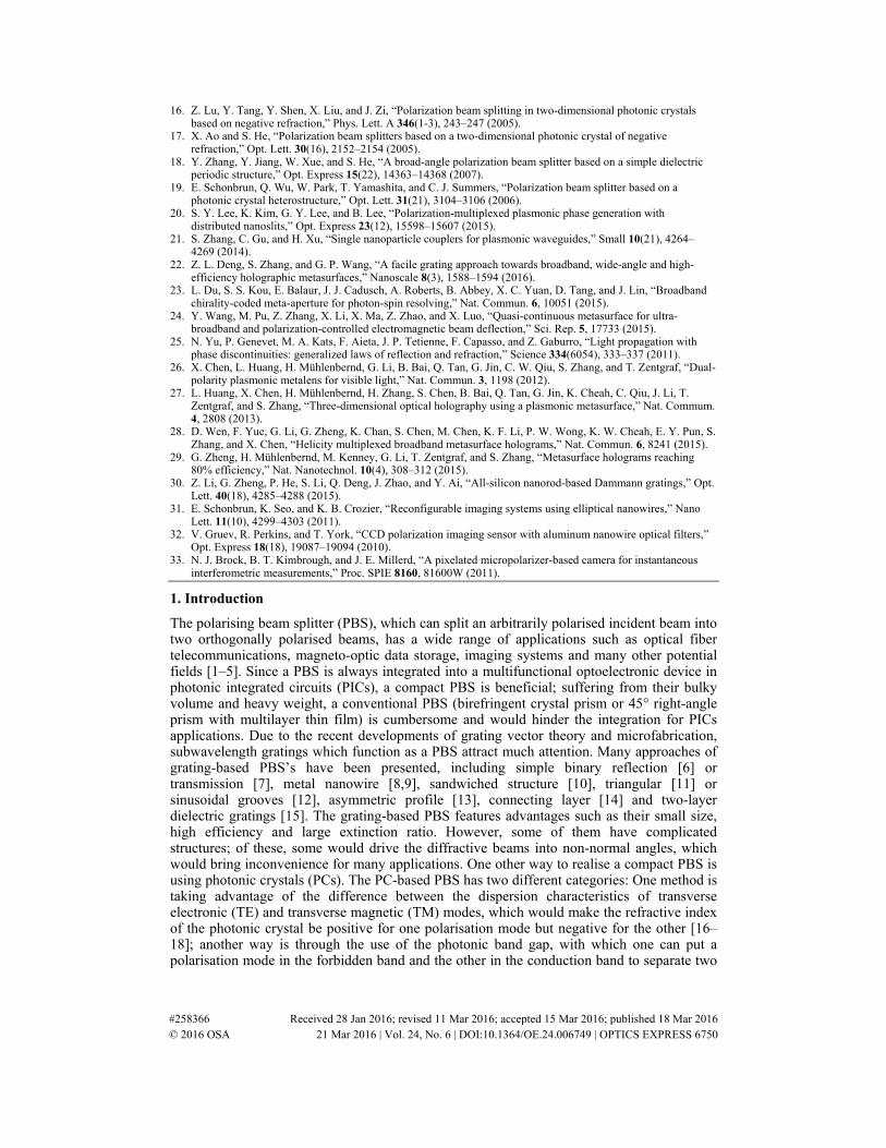
The resonance effect which occurs in the nanobrick has been verified by numerical simulations. We used the commercially available software COMSOL (www.comsol.com) to perform these numerical simulations. The incident electromagnetic field was assumed to be a plane wave whose wavelength is 1547.5 nm (corresponding to the central wavelength of the C-band of optical fiber telecommunications windows), propagating along the negative z-axis with electric and magnetic field vectors lying in the x-y plane (the coordinate system is shown in Fig. 1), where the electric and magnetic fields are naturally orthogonal to each other. Since periodic boundary conditions were utilised in the model, only zeroth-order diffraction beams were propagating. Following this, the transmitted beams were collected by field ports and we retrieved the reflected and transmitted beams from the data to determine the reflection and transmission efficiency. Here, when waves propagate with polarisation direction aligned with the long axis of the nanobricks (x-axis), the reflectivity and transmissivity are labelled correspondingly as Rx and Tx, respectively. Conversely, when waves propagate with polarisation direction along the short axis of the nanobricks (y-axis), the reflectivity and transmissivity are marked as Ry and Ty, respectively. Using these definitions, we swept the dimensions and cell size of a nanobrick to optimize the performance, where the simulated results are shown in Figs. 2(a)-2(d).
In Fig. 2(a), we swept H (the height of a nanobrick) whilst keeping the other dimension parameters unchanged. It can be seen that the transmissivity Ty stays above 93% with slight periodic undulations when H ranges from 100 nm to 2000 nm. On the other hand, the reflectivity Ry remains below 7% and follows the compensated trend of Ty when H varies. These results are of interest; silicon has a high refractive index of around 3.67 which would cause a high reflection, but a silicon nanobrick sitting atop a glass substrate has a similar transmissivity to that of a bulk glass (~96% for normal incidence). This implies that the nanobrick is nearly transparent to the electromagnetic wave at the operation wavelength and that light with its polarisation direction along the y-axis is far away from the resonance region. We explain this high transmission of light polarised along the y-axis by two reasons: Firstly, the “equivalent refractive index” of a silicon nanobrick in the y-axis direction is far lower than that of a bulk silicon refractive index (~3.67), where we assume the value is slightly bigger than the refractive index of glass (~1.51) since they have similar reflectivity (~4% for Fresnel reflection); Secondly, the nanobrick layer acts as a Fabry–Pérot cavity which causes multiple beam interferences where this accounts for the periodic fluctuations of Ty and Ry when H is varied.
The situation for the x-axis is quite different; as can be seen in Fig. 2(a), there are two periodic peak-to-valley fluctuations for the reflectivity Rx and the transmissivity Tx when H ranges from 100 nm to 2000 nm, which implies that the phenomenon of resonance is occurring. To investigate the resonance region, we set H as 490 nm (this value falls into the ranges of peak response) and used CST Microwave Studio software to perform the numerical simulations. The electric field distributions of an incident wave polarised along the x- and y-
#258366 Received 28 Jan 2016; revised 11 Mar 2016; accepted 15 Mar 2016; published 18 Mar 2016 © 2016 OSA 21 Mar 2016 | Vol. 24, No. 6 | DOI:10.1364/OE.24.006749 | OPTICS EXPRESS 6752

axes are shown as Fig. 2(b), which indicates that the incident waves polarised along the long and short axes of a nanobrick are almost reflected and transmitted, respectively. Following this, we plotted the electric and magnetic fields at the cross-section of a nanobrick, shown in Figs. 2(c) and 2(d), from where we can observe that magnetic resonance occurs, with magnetic field enhancement at the center of the y−z plane and vortex-like electric fields circulating in the x−z plane. In essence, it is observed from Figs. 2(a)-2(d) that the anisotropic behavior causes a significant difference for the transmission between the two orthogonally polarised modes, confirming the role of the nanobricks as a high-efficiency PBS.
From Fig. 2(a), it is also observed that the position of peak transmissivity Ty does not coincide with that of reflectivity Rx. This contradiction can be alleviated by choosing a relatively large value of nanobrick height, ~1500 nm e. g., since Rx and Ty have different fluctuation periods. However, a large nanobrick height would bring a high depth-width ratio, which would increase the fabrication difficulties.
Fig. 2. (a) Simulated reflectivity and transmissivity Rx, Ry, Tx and Ty with the height of the nanobricks varying from 100 nm to 2000 nm. Here R and T refer to the reflected wave and transmitted wave, respectively, and x and y denote the long and short axes directions of the nanobrick, respectively. The operation wavelength is fixed at 1547.5 nm. (b) Electric fields of x-polarised and y-polarised light in the simulation domain. (c-d) The vortex-like electric field distribution (c) and magnetic field enhancement at the center of silicon nanobricks (d) indicate magnetic resonance. In the numerical simulations, the dimensions of a nanobrick are fixed with cell size of 720 nm, length of 400 nm, width of 210 nm and height of 490 nm.
3. Performance analysis
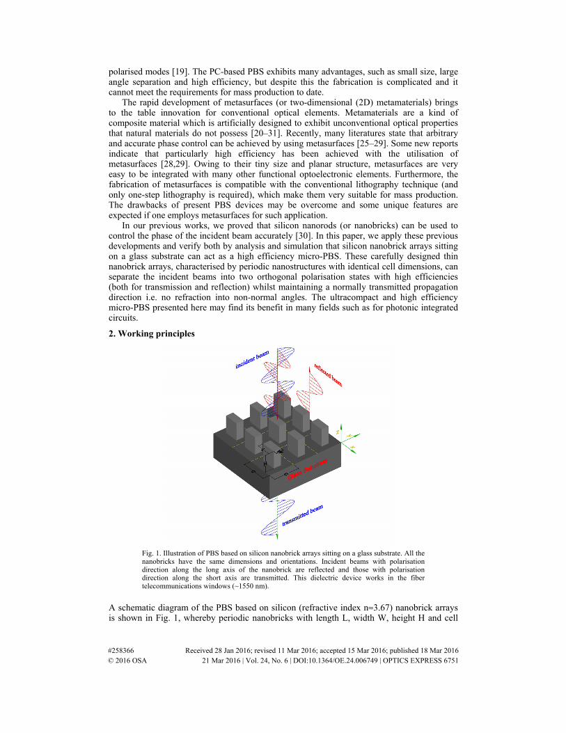
To obtain the best polarisation separation efficiency determined by the difference between Rx and Ty simultaneously, all structural parameters of the nanobrick-based PBS were optimised by using COMSOL software. The design results are with cell size C of 720 nm, length L of 400 nm, width W of 210 nm and height H of 490 nm. The high polarisation separation efficiency is verified by numerical simulations for a uniform metasurface with all nanobricks aligned along the same direction, as shown in Fig. 3(a). For the specific geometry configuration shown in Fig. 1 upon normal light incidence, the numerical simulations show
#258366 Received 28 Jan 2016; revised 11 Mar 2016; accepted 15 Mar 2016; published 18 Mar 2016 © 2016 OSA 21 Mar 2016 | Vol. 24, No. 6 | DOI:10.1364/OE.24.006749 | OPTICS EXPRESS 6753
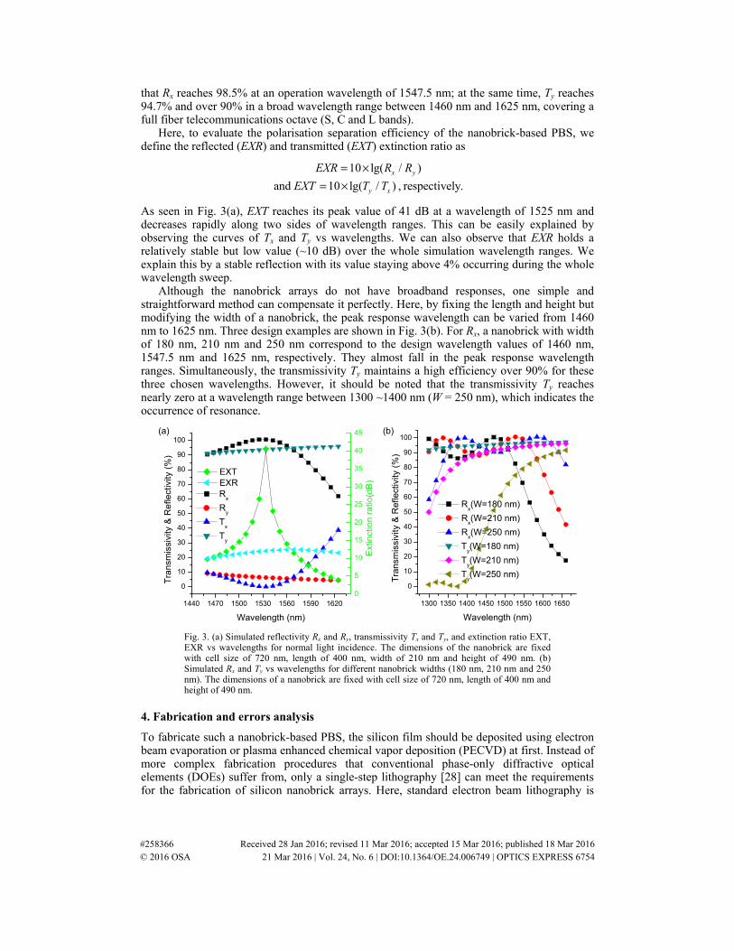
that Rx reaches 98.5% at an operation wavelength of 1547.5 nm; at the same time, Ty reaches 94.7% and over 90% in a broad wavelength range between 1460 nm and 1625 nm, covering a full fiber telecommunications octave (S, C and L bands).
Here, to evaluate the polarisation separation efficiency of the nanobrick-based PBS, we define the reflected (EXR) and transmitted (EXT) extinction ratio as
10 lg( / )
and 10 lg( / ) , respectively.x y
y x
EXR R R
EXT T T
= ×= ×
As seen in Fig. 3(a), EXT reaches its peak value of 41 dB at a wavelength of 1525 nm and decreases rapidly along two sides of wavelength ranges. This can be easily explained by observing the curves of Tx and Ty vs wavelengths. We can also observe that EXR holds a relatively stable but low value (~10 dB) over the whole simulation wavelength ranges. We explain this by a stable reflection with its value staying above 4% occurring during the whole wavelength sweep.
Although the nanobrick arrays do not have broadband responses, one simple and straightforward method can compensate it perfectly. Here, by fixing the length and height but modifying the width of a nanobrick, the peak response wavelength can be varied from 1460 nm to 1625 nm. Three design examples are shown in Fig. 3(b). For Rx, a nanobrick with width of 180 nm, 210 nm and 250 nm correspond to the design wavelength values of 1460 nm, 1547.5 nm and 1625 nm, respectively. They almost fall in the peak response wavelength ranges. Simultaneously, the transmissivity Ty maintains a high efficiency over 90% for these three chosen wavelengths. However, it should be noted that the transmissivity Ty reaches nearly zero at a wavelength range between 1300 ~1400 nm (W = 250 nm), which indicates the occurrence of resonance.
1440 1470 1500 1530 1560 1590 1620
0
10
20
30
40
50
60
70
80
90
100
1300 1350 1400 1450 1500 1550 1600 1650
0
10
20
30
40
50
60
70
80
90
100
Tra
nsm
issi
vity
& R
efle
ctiv
ity (
%)
Wavelength (nm)
Rx
Ry
Tx
Ty
0
5
10
15
20
25
30
35
40
45 (b)
EXT EXR
Ext
inct
ion
ratio
(dB
)
(a)
Tra
nsm
issi
vity
& R
efle
ctiv
ity (
%)
Wavelength (nm)
Rx(W=180 nm)
Rx(W=210 nm)
Rx(W=250 nm)
Ty(W=180 nm)
Ty(W=210 nm)
Ty(W=250 nm)
Fig. 3. (a) Simulated reflectivity Rx and Ry, transmissivity Tx and Ty, and extinction ratio EXT, EXR vs wavelengths for normal light incidence. The dimensions of the nanobrick are fixed with cell size of 720 nm, length of 400 nm, width of 210 nm and height of 490 nm. (b) Simulated Rx and Ty vs wavelengths for different nanobrick widths (180 nm, 210 nm and 250 nm). The dimensions of a nanobrick are fixed with cell size of 720 nm, length of 400 nm and height of 490 nm.
4. Fabrication and errors analysis
To fabricate such a nanobrick-based PBS, the silicon film should be deposited using electron beam evaporation or plasma enhanced chemical vapor deposition (PECVD) at first. Instead of more complex fabrication procedures that conventional phase-only diffractive optical elements (DOEs) suffer from, only a single-step lithography [28] can meet the requirements for the fabrication of silicon nanobrick arrays. Here, standard electron beam lithography is
#258366 Received 28 Jan 2016; revised 11 Mar 2016; accepted 15 Mar 2016; published 18 Mar 2016 © 2016 OSA 21 Mar 2016 | Vol. 24, No. 6 | DOI:10.1364/OE.24.006749 | OPTICS EXPRESS 6754
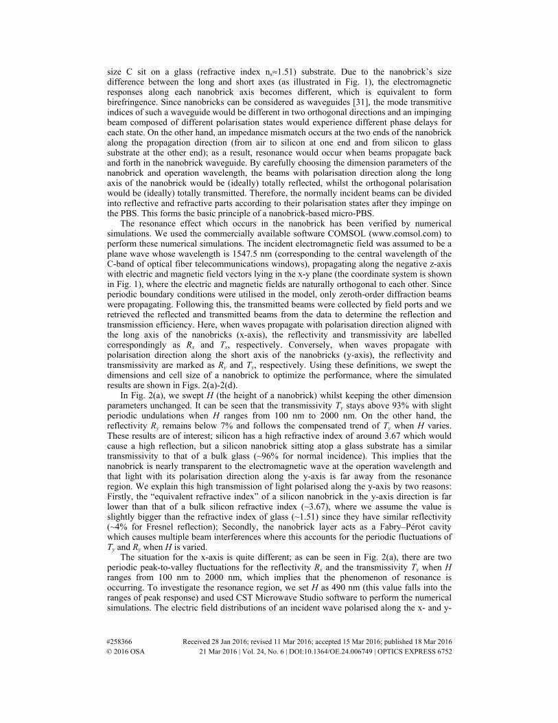
used to develop the nanobrick pattern primarily. Following this, the pattern is etched directly by reactive ion etching (RIE). Since the aspect ratio of our nanostructure (2.3 at short axis and 1.2 at long axis direction in our design example) is not very large, the fabrication errors would not greatly diminish the performance.
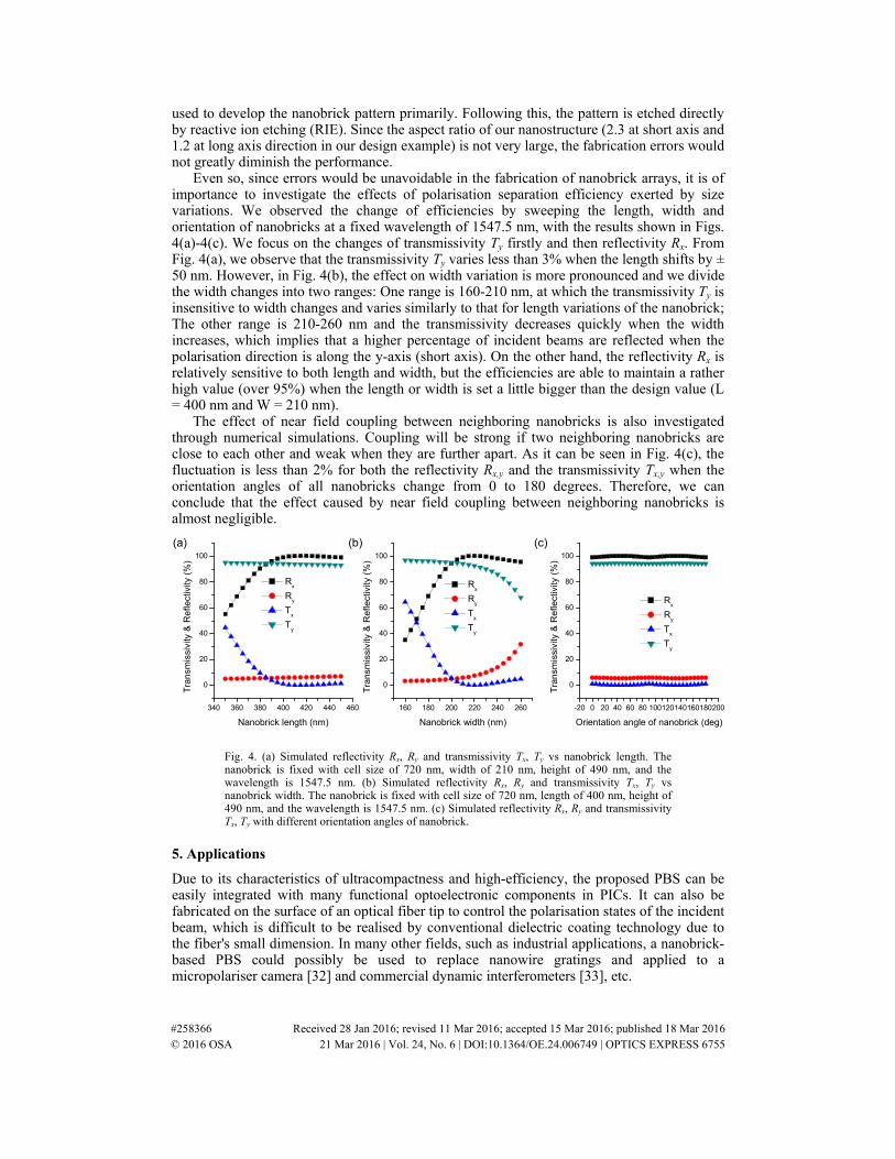
Even so, since errors would be unavoidable in the fabrication of nanobrick arrays, it is of importance to investigate the effects of polarisation separation efficiency exerted by size variations. We observed the change of efficiencies by sweeping the length, width and orientation of nanobricks at a fixed wavelength of 1547.5 nm, with the results shown in Figs. 4(a)-4(c). We focus on the changes of transmissivity Ty firstly and then reflectivity Rx. From Fig. 4(a), we observe that the transmissivity Ty varies less than 3% when the length shifts by ± 50 nm. However, in Fig. 4(b), the effect on width variation is more pronounced and we divide the width changes into two ranges: One range is 160-210 nm, at which the transmissivity Ty is insensitive to width changes and varies similarly to that for length variations of the nanobrick; The other range is 210-260 nm and the transmissivity decreases quickly when the width increases, which implies that a higher percentage of incident beams are reflected when the polarisation direction is along the y-axis (short axis). On the other hand, the reflectivity Rx is relatively sensitive to both length and width, but the efficiencies are able to maintain a rather high value (over 95%) when the length or width is set a little bigger than the design value (L = 400 nm and W = 210 nm).
The effect of near field coupling between neighboring nanobricks is also investigated through numerical simulations. Coupling will be strong if two neighboring nanobricks are close to each other and weak when they are further apart. As it can be seen in Fig. 4(c), the fluctuation is less than 2% for both the reflectivity Rx,y and the transmissivity Tx,y when the orientation angles of all nanobricks change from 0 to 180 degrees. Therefore, we can conclude that the effect caused by near field coupling between neighboring nanobricks is almost negligible.
340 360 380 400 420 440 460
0
20
40
60
80
100
160 180 200 220 240 260
0
20
40
60
80
100
-20 0 20 40 60 80 100120140160180200
0
20
40
60
80
100
(c)(b)
Tra
nsm
issi
vity
& R
efle
ctiv
ity (
%)
Nanobrick length (nm)
Rx
Ry
Tx
Ty
(a)
Tra
nsm
issi
vity
& R
efle
ctiv
ity (
%)
Nanobrick width (nm)
Rx
Ry
Tx
Ty
Tra
nsm
issi
vity
& R
efle
ctiv
ity (
%)
Orientation angle of nanobrick (deg)
Rx
Ry
Tx
Ty
Fig. 4. (a) Simulated reflectivity Rx, Ry and transmissivity Tx, Ty vs nanobrick length. The nanobrick is fixed with cell size of 720 nm, width of 210 nm, height of 490 nm, and the wavelength is 1547.5 nm. (b) Simulated reflectivity Rx, Ry and transmissivity Tx, Ty vs nanobrick width. The nanobrick is fixed with cell size of 720 nm, length of 400 nm, height of 490 nm, and the wavelength is 1547.5 nm. (c) Simulated reflectivity Rx, Ry and transmissivity Tx, Ty with different orientation angles of nanobrick.
5. Applications
Due to its characteristics of ultracompactness and high-efficiency, the proposed PBS can be easily integrated with many functional optoelectronic components in PICs. It can also be fabricated on the surface of an optical fiber tip to control the polarisation states of the incident beam, which is difficult to be realised by conventional dielectric coating technology due to the fiber's small dimension. In many other fields, such as industrial applications, a nanobrick-based PBS could possibly be used to replace nanowire gratings and applied to a micropolariser camera [32] and commercial dynamic interferometers [33], etc.
#258366 Received 28 Jan 2016; revised 11 Mar 2016; accepted 15 Mar 2016; published 18 Mar 2016 © 2016 OSA 21 Mar 2016 | Vol. 24, No. 6 | DOI:10.1364/OE.24.006749 | OPTICS EXPRESS 6755
Apart from these, a nanobrick-based PBS can also be used as a phase-delay modulator and used to change the direction of beam propagation. To prove this, we consider a normally
incident circularly polarised (CP) beam, with a Jones vector of 1
i
±
, impinging onto a
nanobrick with its orientation direction (short-axis) forming an angle φ with the x axis. Since a nanobrick-based PBS can be considered as a micropolariser in the transmission direction, the Jones vector of the transmission beam can be expressed as
21 cos 2 sin 2 1 1 11 1 1. .
sin 2 1 cos 22 2 2ie
i i iϕϕ ϕ
ϕ ϕ±+
= + − ± ± (1)
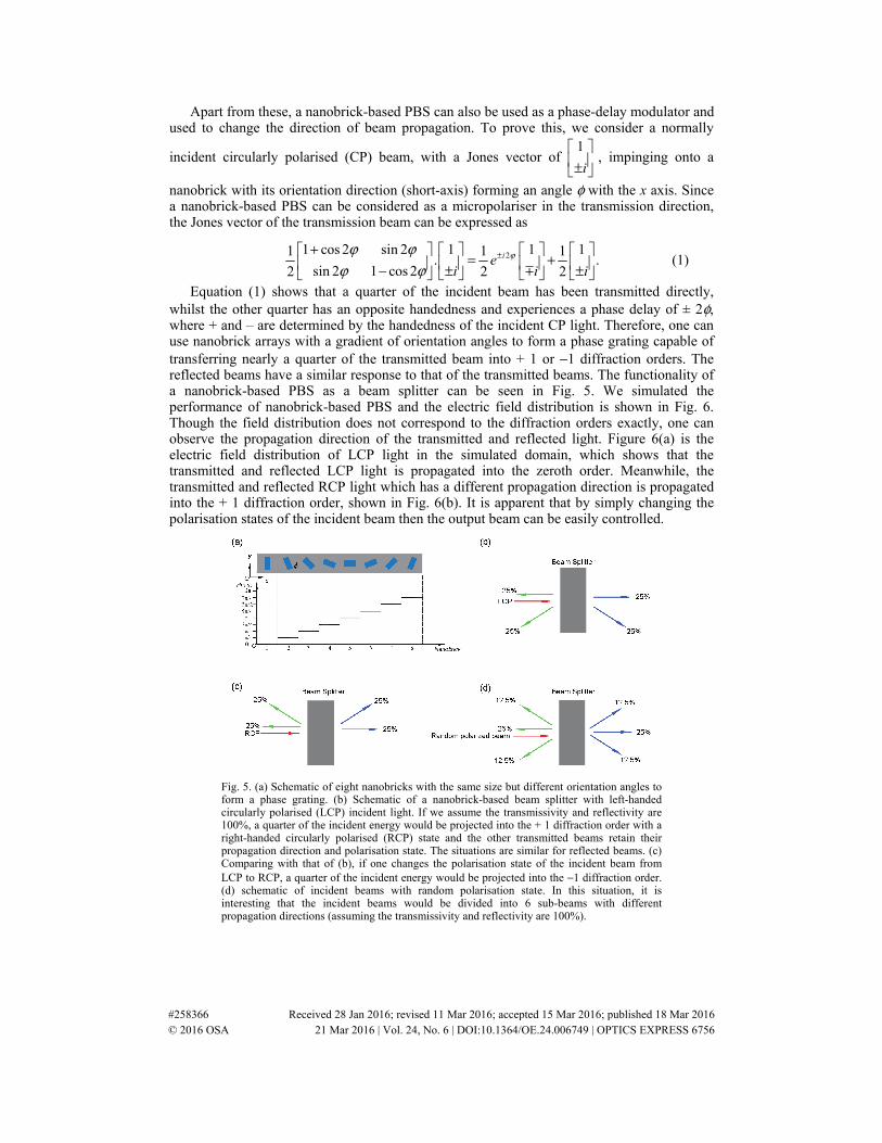
Equation (1) shows that a quarter of the incident beam has been transmitted directly, whilst the other quarter has an opposite handedness and experiences a phase delay of ± 2φ, where + and – are determined by the handedness of the incident CP light. Therefore, one can use nanobrick arrays with a gradient of orientation angles to form a phase grating capable of transferring nearly a quarter of the transmitted beam into + 1 or −1 diffraction orders. The reflected beams have a similar response to that of the transmitted beams. The functionality of a nanobrick-based PBS as a beam splitter can be seen in Fig. 5. We simulated the performance of nanobrick-based PBS and the electric field distribution is shown in Fig. 6. Though the field distribution does not correspond to the diffraction orders exactly, one can observe the propagation direction of the transmitted and reflected light. Figure 6(a) is the electric field distribution of LCP light in the simulated domain, which shows that the transmitted and reflected LCP light is propagated into the zeroth order. Meanwhile, the transmitted and reflected RCP light which has a different propagation direction is propagated into the + 1 diffraction order, shown in Fig. 6(b). It is apparent that by simply changing the polarisation states of the incident beam then the output beam can be easily controlled.
Fig. 5. (a) Schematic of eight nanobricks with the same size but different orientation angles to form a phase grating. (b) Schematic of a nanobrick-based beam splitter with left-handed circularly polarised (LCP) incident light. If we assume the transmissivity and reflectivity are 100%, a quarter of the incident energy would be projected into the + 1 diffraction order with a right-handed circularly polarised (RCP) state and the other transmitted beams retain their propagation direction and polarisation state. The situations are similar for reflected beams. (c) Comparing with that of (b), if one changes the polarisation state of the incident beam from LCP to RCP, a quarter of the incident energy would be projected into the −1 diffraction order. (d) schematic of incident beams with random polarisation state. In this situation, it is interesting that the incident beams would be divided into 6 sub-beams with different propagation directions (assuming the transmissivity and reflectivity are 100%).
#258366 Received 28 Jan 2016; revised 11 Mar 2016; accepted 15 Mar 2016; published 18 Mar 2016 © 2016 OSA 21 Mar 2016 | Vol. 24, No. 6 | DOI:10.1364/OE.24.006749 | OPTICS EXPRESS 6756
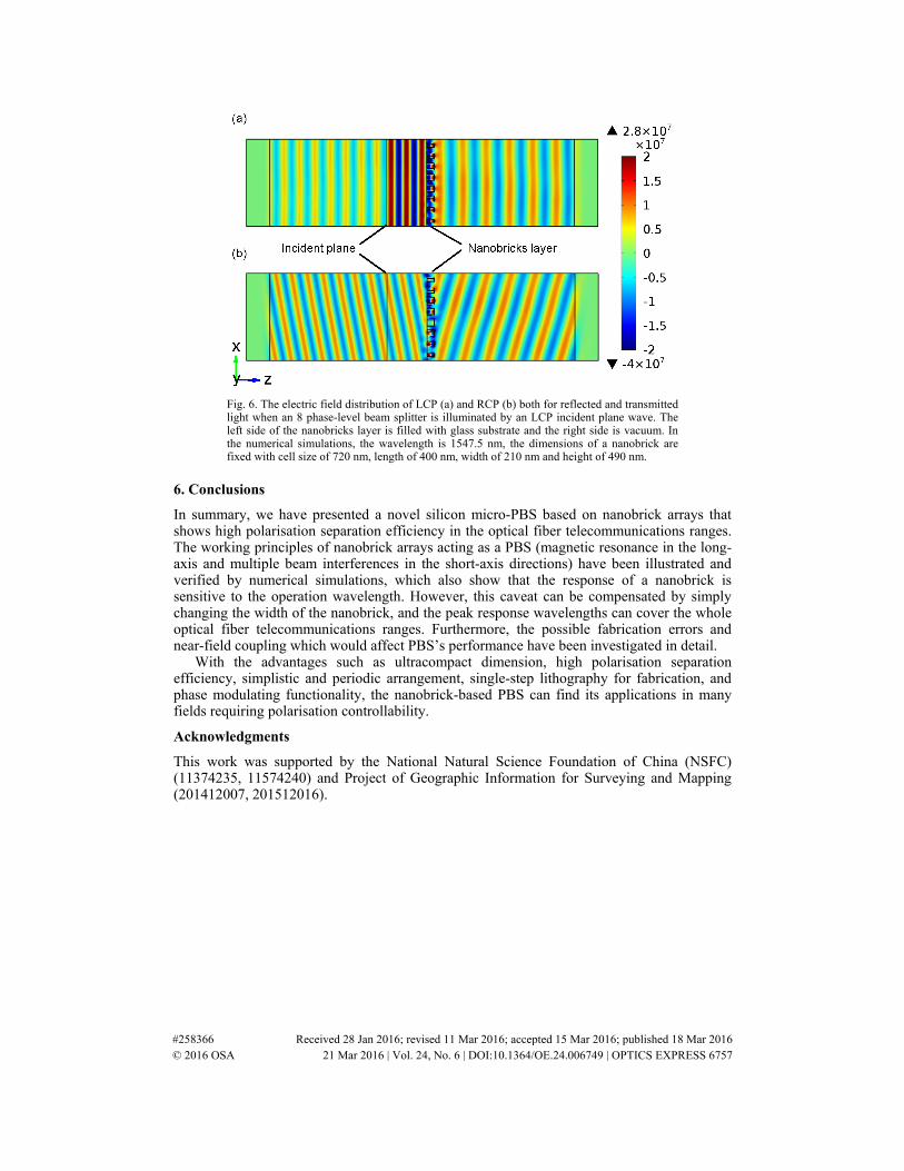
Fig. 6. The electric field distribution of LCP (a) and RCP (b) both for reflected and transmitted light when an 8 phase-level beam splitter is illuminated by an LCP incident plane wave. The left side of the nanobricks layer is filled with glass substrate and the right side is vacuum. In the numerical simulations, the wavelength is 1547.5 nm, the dimensions of a nanobrick are fixed with cell size of 720 nm, length of 400 nm, width of 210 nm and height of 490 nm.
6. Conclusions
In summary, we have presented a novel silicon micro-PBS based on nanobrick arrays that shows high polarisation separation efficiency in the optical fiber telecommunications ranges. The working principles of nanobrick arrays acting as a PBS (magnetic resonance in the long-axis and multiple beam interferences in the short-axis directions) have been illustrated and verified by numerical simulations, which also show that the response of a nanobrick is sensitive to the operation wavelength. However, this caveat can be compensated by simply changing the width of the nanobrick, and the peak response wavelengths can cover the whole optical fiber telecommunications ranges. Furthermore, the possible fabrication errors and near-field coupling which would affect PBS’s performance have been investigated in detail.
With the advantages such as ultracompact dimension, high polarisation separation efficiency, simplistic and periodic arrangement, single-step lithography for fabrication, and phase modulating functionality, the nanobrick-based PBS can find its applications in many fields requiring polarisation controllability.
Acknowledgments
This work was supported by the National Natural Science Foundation of China (NSFC) (11374235, 11574240) and Project of Geographic Information for Surveying and Mapping (201412007, 201512016).
#258366 Received 28 Jan 2016; revised 11 Mar 2016; accepted 15 Mar 2016; published 18 Mar 2016 © 2016 OSA 21 Mar 2016 | Vol. 24, No. 6 | DOI:10.1364/OE.24.006749 | OPTICS EXPRESS 6757