ultrascale ddr4 de-emphasis and ctle feature optimization … · and ctle feature optimization with...
TRANSCRIPT

ULTRASCALE DDR4 DE-EMPHASIS AND CTLE FEATURE OPTIMIZATION WITH STATISTICAL ENGINE FOR BER
SPECIFICATION

Penglin Niu, [email protected]
Fangyi Rao, [email protected]
Juan Wang, [email protected]
Gary Otonari, [email protected]
Nilesh Kamdar, [email protected]
Yong Wang, [email protected]
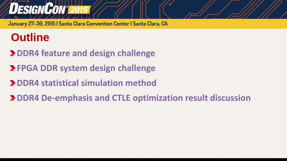
Outline
DDR4 feature and design challenge
FPGA DDR system design challenge
DDR4 statistical simulation method
DDR4 De-emphasis and CTLE optimization result discussion
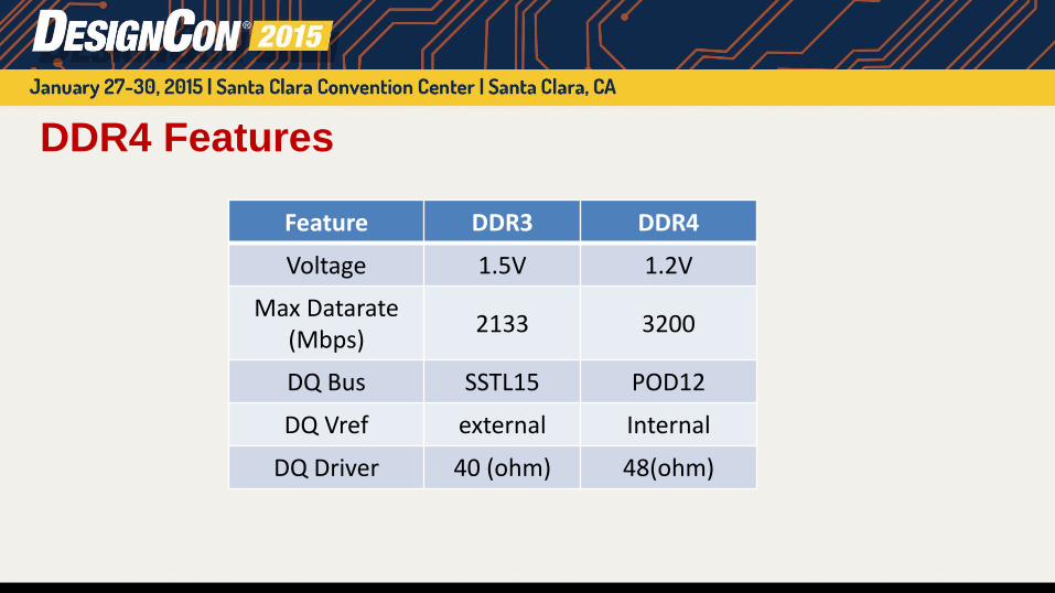
DDR4 Features
Feature DDR3 DDR4
Voltage 1.5V 1.2V
Max Datarate (Mbps)
2133 3200
DQ Bus SSTL15 POD12
DQ Vref external Internal
DQ Driver 40 (ohm) 48(ohm)

FPGA DDR4 Design Challenges DDR4 Design Challenge
– Higher datarate, Higher loss, intensified ISI
FPGA Configurable I/O standards
– DDR3, DDR3L, DDR4, LPDDR2, LPDDR3, RLDRAM3, QDR2+, QDR4
– High pad capacitance: FPGA ~3.5pF Vs. ~1.8pF ASIC
FPGA High I/O count
– Up to ~1400 IO counts in Ultrascale family
– High density signal routing
– High signal to ground ratio
Signal enhancement techniques to mitigate
– De-emphasis & CTLE

FPGA DDR4
Design
Challenges
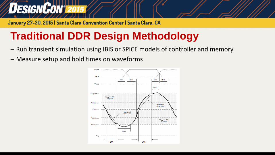
Traditional DDR Design Methodology – Run transient simulation using IBIS or SPICE models of controller and memory
– Measure setup and hold times on waveforms
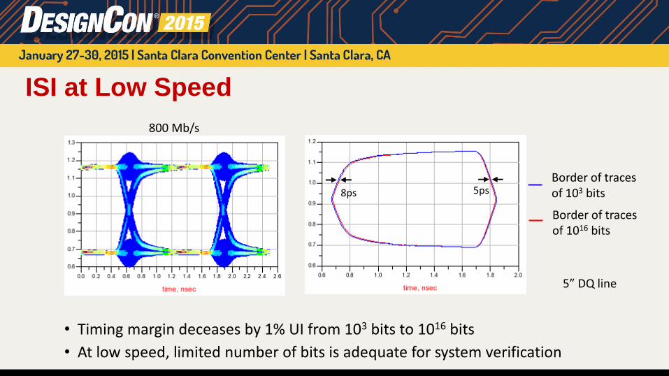
ISI at Low Speed
800 Mb/s
Border of traces of 103 bits
Border of traces of 1016 bits
8ps 5ps
• Timing margin deceases by 1% UI from 103 bits to 1016 bits
• At low speed, limited number of bits is adequate for system verification
5” DQ line
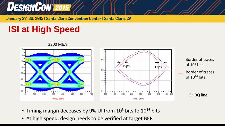
ISI at High Speed
Border of traces of 103 bits
Border of traces of 1016 bits
5” DQ line
15ps 13ps
3200 Mb/s
• Timing margin deceases by 9% UI from 103 bits to 1016 bits
• At high speed, design needs to be verified at target BER
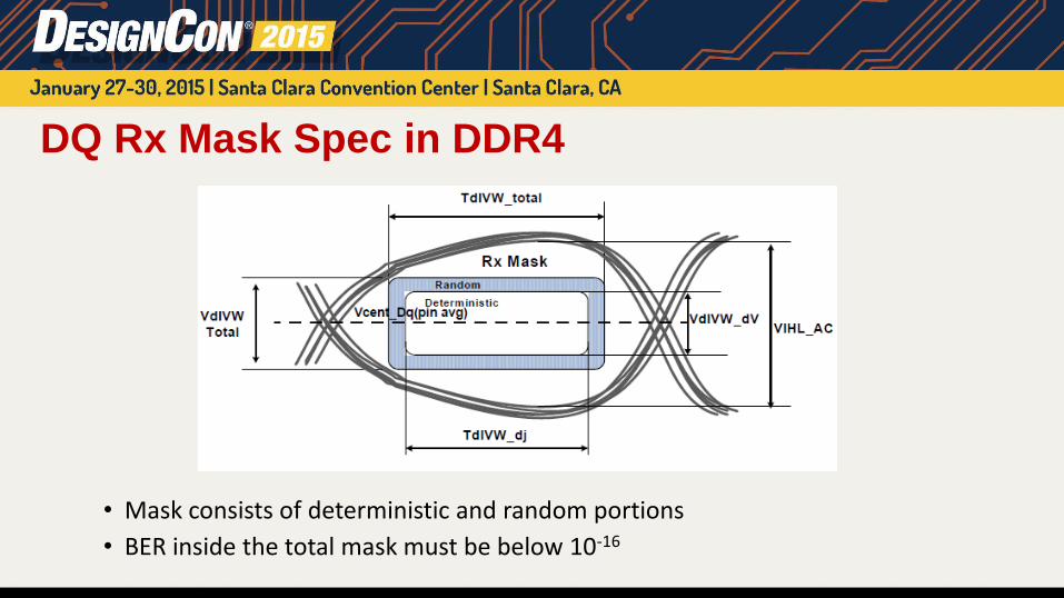
DQ Rx Mask Spec in DDR4
• Mask consists of deterministic and random portions
• BER inside the total mask must be below 10-16
Statistical Simulation for BER
• It’s impractical to simulate 1016 bits to estimate BER at 10-16
• Statistical method can be employed to calculate eye probability distributions
• Equivalent to running infinite number of bits
• BER can be obtained rigorously at arbitrarily low level
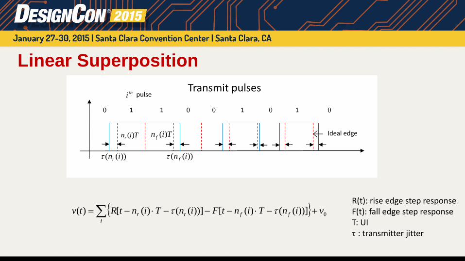
Linear Superposition
Tinr )( Tin f )(
))(( inr ))(( in f
0 1 1 0 0 1 0 1 0
pulse
Ideal edge
thi
0))](()([))](()([)( vinTintFinTintRtvi
ffrr R(t): rise edge step response F(t): fall edge step response T: UI : transmitter jitter
Transmit pulses

Transmitter Jitter
𝜏 𝑛𝑓 =𝐷𝐶𝐷𝑝𝑝
𝑑𝑎𝑡𝑎
2− −1 𝑛𝑓
𝐷𝐶𝐷𝑝𝑝𝑐𝑙𝑘
2+ 𝐴𝑠𝑖𝑛(2𝜋𝑓𝑛𝑓𝑇 + 𝜙) + 𝜌(𝑛𝑓)
𝜏 𝑛𝑟 = −𝐷𝐶𝐷𝑝𝑝
𝑑𝑎𝑡𝑎
2− −1 𝑛𝑟
𝐷𝐶𝐷𝑝𝑝𝑐𝑙𝑘
2+ 𝐴𝑠𝑖𝑛(2𝜋𝑓𝑛𝑟𝑇 + 𝜙) + 𝜌(𝑛𝑟)
𝐷𝐶𝐷𝑝𝑝𝑑𝑎𝑡𝑎 : peak-to-peak data DCD
𝐷𝐶𝐷𝑝𝑝𝑐𝑙𝑘 : peak-to-peak clock DCD
A & f: SJ amplitude and frequency
r: RJ
Jitter components include DCD, SJ and RJ
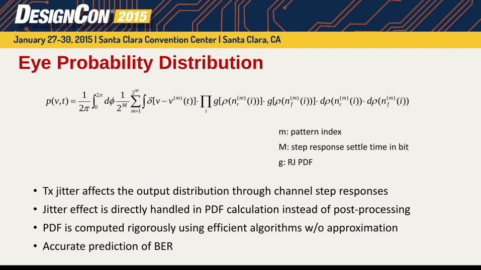
Eye Probability Distribution
rrrr
2
0
2
1
)()()()()( ))(())(())](([))](([)]([2
1
2
1),(
M
m
m
f
m
r
m
f
i
m
r
m
Mindindingingtvvdtvp
m: pattern index
M: step response settle time in bit
g: RJ PDF
• Tx jitter affects the output distribution through channel step responses
• Jitter effect is directly handled in PDF calculation instead of post-processing
• PDF is computed rigorously using efficient algorithms w/o approximation
• Accurate prediction of BER
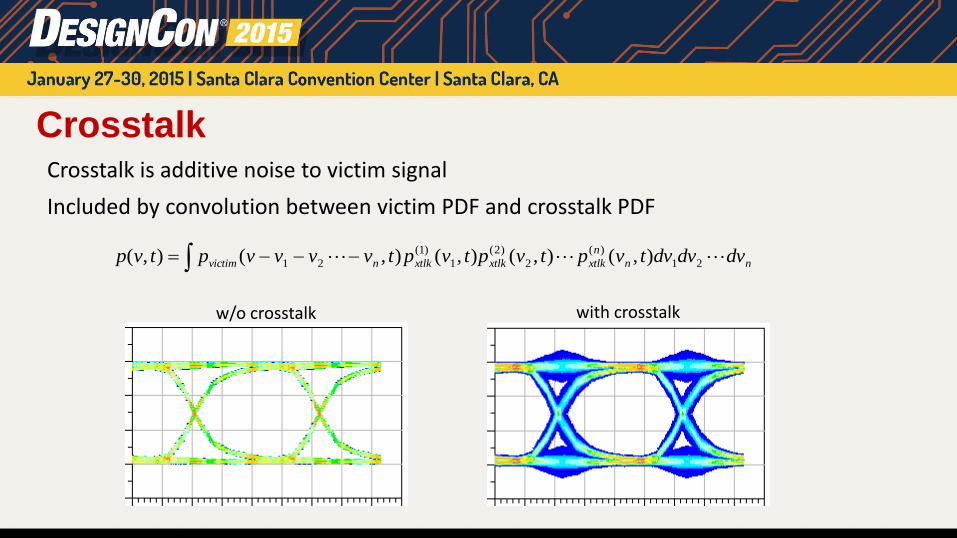
Crosstalk Crosstalk is additive noise to victim signal
Included by convolution between victim PDF and crosstalk PDF
nn
n
xtlkxtlkxtlknvictim dvdvdvtvptvptvptvvvvptvp 21
)(
2
)2(
1
)1(
21 ),(),(),(),(),(
with crosstalk w/o crosstalk

Driver De-emphasis
w/o de-emphasis 3dB de-emphasis
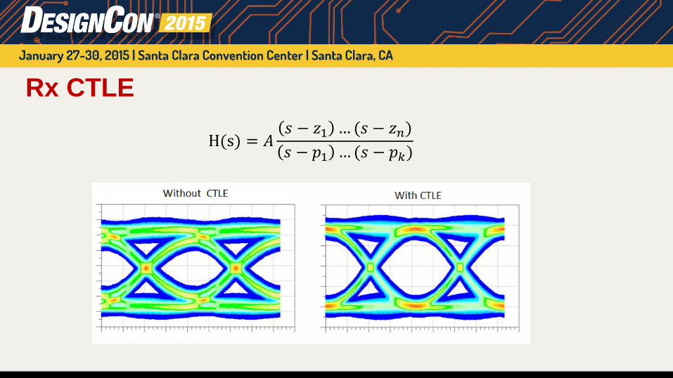
Rx CTLE
H(s) = 𝐴𝑠 − 𝑧1 …(𝑠 − 𝑧𝑛)
𝑠 − 𝑝1 …(𝑠 − 𝑝𝑘)

Asymmetric Rise and Fall Edges Capability
rise time < fall time rise time > fall time
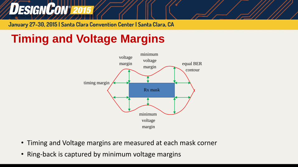
Timing and Voltage Margins
timing margin
voltage
margin
minimum
voltage
margin
minimum
voltage
margin
Rx mask
equal BER
contour
• Timing and Voltage margins are measured at each mask corner
• Ring-back is captured by minimum voltage margins

DDR4 Channel Topology
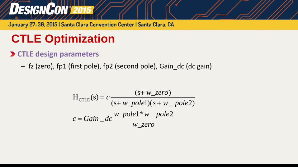
CTLE Optimization
CTLE design parameters
– fz (zero), fp1 (first pole), fp2 (second pole), Gain_dc (dc gain)
w_zero
poleww_poledcGainc
polewsw_pole
w_zeroc
2_*1_
)2_)(1(s
)(s(s)HCTLE

CTLE Optimization
CTLE fz sensitivity sweep for
two study channels
– BER 10-16 eye width @ Vref
+/-68mV saturated after
600Mhz fz
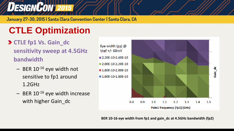
CTLE Optimization
CTLE fp1 Vs. Gain_dc
sensitivity sweep at 4.5GHz
bandwidth
– BER 10-16 eye width not
sensitive to fp1 around
1.2GHz
– BER 10-16 eye width increase
with higher Gain_dc
BER 10-16 eye width from fp1 and gain_dc at 4.5GHz bandwidth (fp2)

CTLE Optimization
CTLE fp1 Vs. Gain_dc
sensitivity sweep at 6 GHz
bandwidth
– BER 10-16 eye width not very
sensitive to fp2 around 5GHz
– BER 10-16 eye width increase
with higher Gain_dc
BER 10-16 eye width from fp1 and gain_dc at 6GHz bandwidth (fp2)
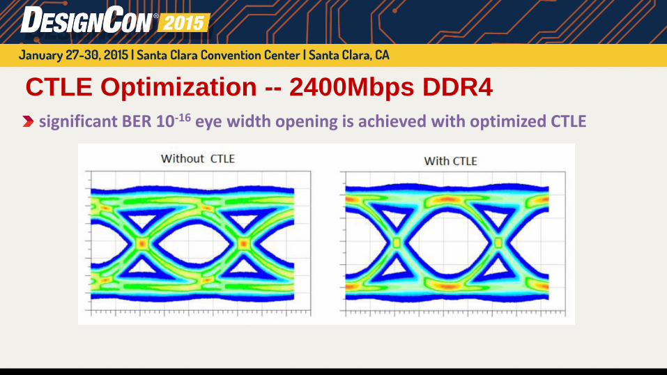
CTLE Optimization -- 2400Mbps DDR4
significant BER 10-16 eye width opening is achieved with optimized CTLE
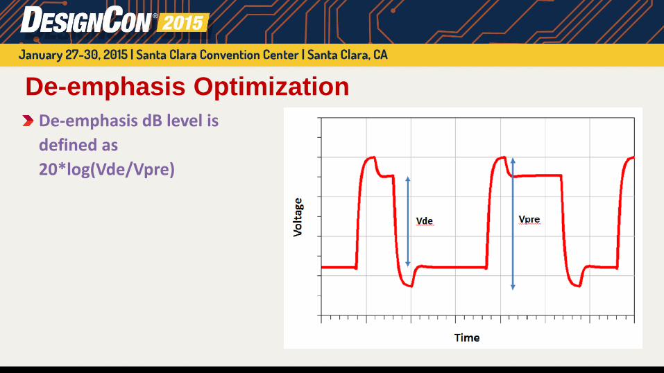
De-emphasis Optimization
De-emphasis dB level is
defined as
20*log(Vde/Vpre)

De-emphasis Optimization
Optimal De-emphasis dB can be identified for driver slew rate

De-emphasis Optimization – 2400Mbps DDR4
10-20ps BER 10-16 eye width opening achieved with optimized dB setting

Summary
A statistical simulation engine is introduced for designing DDR4 system to
JEDEC 10-16 BER target
Effects of driver de-emphasis and Rx CTLE on DDR4 timing at BER target of
10-16 are investigated
De-emphasis and CTLE are effective techniques to mitigate jitter and
achieve DDR4 design target after optimization.