ultrathin gate dielectrics on sige/sigec heterolayers by siddheswar maikap
DESCRIPTION
Ultrathin Gate Dielectrics on SiGe/SiGeC Heterolayers By Siddheswar Maikap Department of Physics Indian Institute of Technology (IIT), Kharagpur India. Who am I ?. IIT, Kharagpur, 1950 IIT, Kanpur, 1963 IIT, Bombay, 1958 IIT, Guwahati, 1994 - PowerPoint PPT PresentationTRANSCRIPT
1
Ultrathin Gate Dielectrics on SiGe/SiGeC
Heterolayers
By
Siddheswar Maikap
Department of Physics
Indian Institute of Technology (IIT), Kharagpur
India

2
Who am I ?
IIT, Kharagpur, 1950 IIT, Kanpur, 1963
IIT, Bombay, 1958 IIT, Guwahati, 1994
IIT, Delhi, 1961 IIT, Roorkee, 2001
IIT, Madras, 1961
3
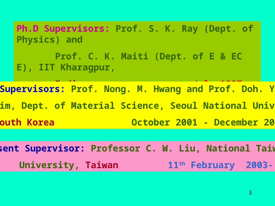
Present Supervisor: Professor C. W. Liu, National Taiwan
University, Taiwan 11th February 2003-
Ph.D Supervisors: Prof. S. K. Ray (Dept. of Physics) and
Prof. C. K. Maiti (Dept. of E & ECE), IIT Kharagpur,
India July 1997 - October 2001
Postdoc Supervisors: Prof. Nong. M. Hwang and Prof. Doh. Y.
Kim, Dept. of Material Science, Seoul National University,
South Korea October 2001 - December 2002
4
Outline of the Work
Introduction
Growth of group-IV alloy layers
Ultrathin oxides on partially strained layers
Extraction of material parameters for
SiGe/SiGeC heterolayers
High-k gate dielectric for alternative SiO2
Conclusion and Future work
5
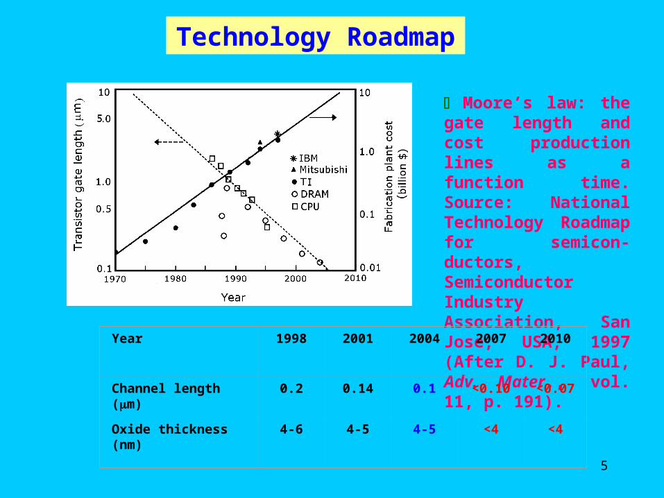
Technology Roadmap
Moore’s law: the gate length and cost production lines as a function time. Source: National Technology Roadmap for semicon-ductors, Semiconductor Industry Association, San Jose, USA, 1997 (After D. J. Paul, Adv. Mater., vol. 11, p. 191).
Year
1998 2001 2004 2007 2010
Channel length (m)
0.2 0.14 0.1 <0.10 <0.07
Oxide thickness (nm)
4-6 4-5 4-5 <4 <4
6
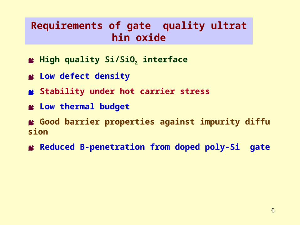
Requirements of gate quality ultrathin oxide
High quality Si/SiO2 interface
Low defect density
Stability under hot carrier stress
Low thermal budget
Good barrier properties against impurity diffusion
Reduced B-penetration from doped poly-Si gate
7
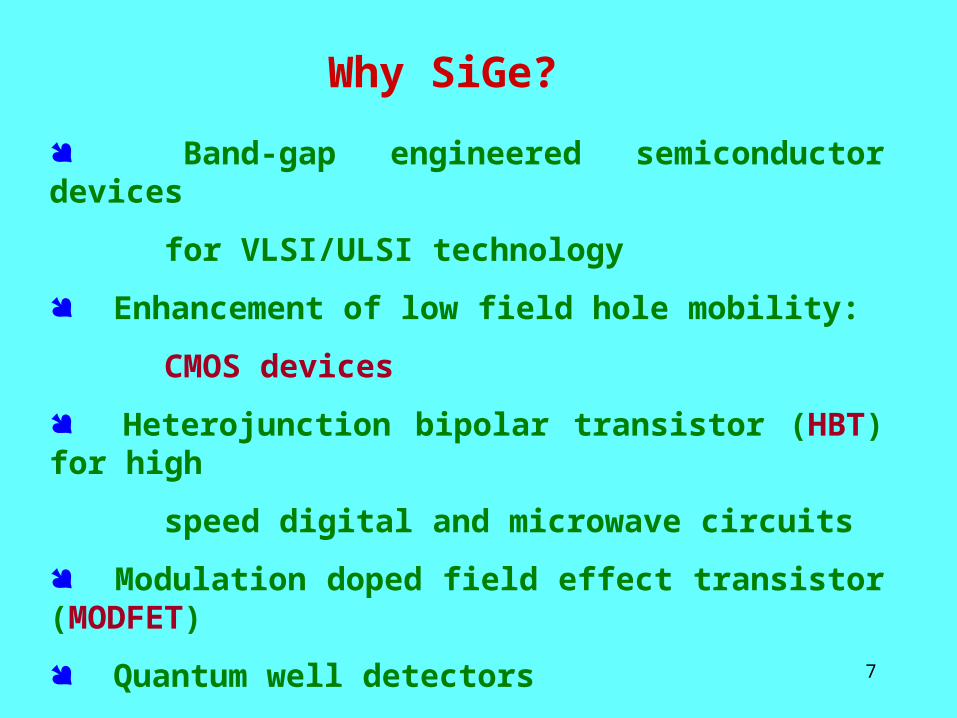
Band-gap engineered semiconductor devices
for VLSI/ULSI technology
Enhancement of low field hole mobility:
CMOS devices
Heterojunction bipolar transistor (HBT) for high
speed digital and microwave circuits
Modulation doped field effect transistor (MODFET)
Quantum well detectors
Resonant tunneling diodes
Why SiGe?
8
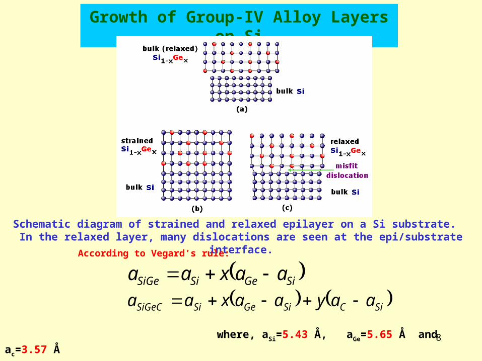
Growth of Group-IV Alloy Layers on Si
Schematic diagram of strained and relaxed epilayer on a Si substrate. In the relaxed layer, many dislocations are seen at the epi/substrate interface.
According to Vegard’s rule:
where, aSi=5.43 Å, aGe=5.65 Å and ac=3.57 Å
SiGeSiSiGe aaxaa SiCSiGeSiSiGeC aayaaxaa
9
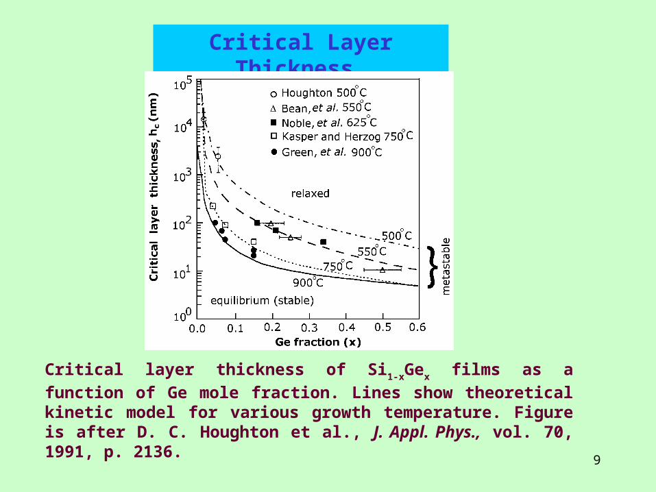
Critical Layer Thickness
Critical layer thickness of Si1-xGex films as a function of Ge mole fraction.
Lines show theoretical kinetic model for various growth temperature. Figure is after D. C. Houghton et al., J. Appl. Phys., vol. 70, 1991, p. 2136.
10
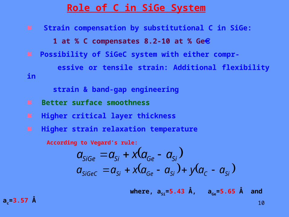
Role of C in SiGe System
Strain compensation by substitutional C in SiGe:
1 at % C compensates 8.2-10 at % Ge
Possibility of SiGeC system with either compr-
essive or tensile strain: Additional flexibility in
strain & band-gap engineering
Better surface smoothness
Higher critical layer thickness
Higher strain relaxation temperature
According to Vegard’s rule:
where, aSi=5.43 Å, aGe=5.65 Å and ac=3.57 Å
SiGeSiSiGe aaxaa SiCSiGeSiSiGeC aayaaxaa
11
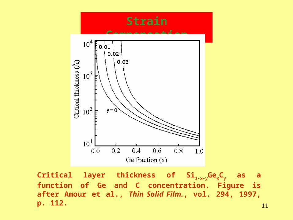
Strain Compensation
Critical layer thickness of Si1-x-yGexCy as a function of Ge and C
concentration. Figure is after Amour et al., Thin Solid Film., vol. 294, 1997, p. 112.
12
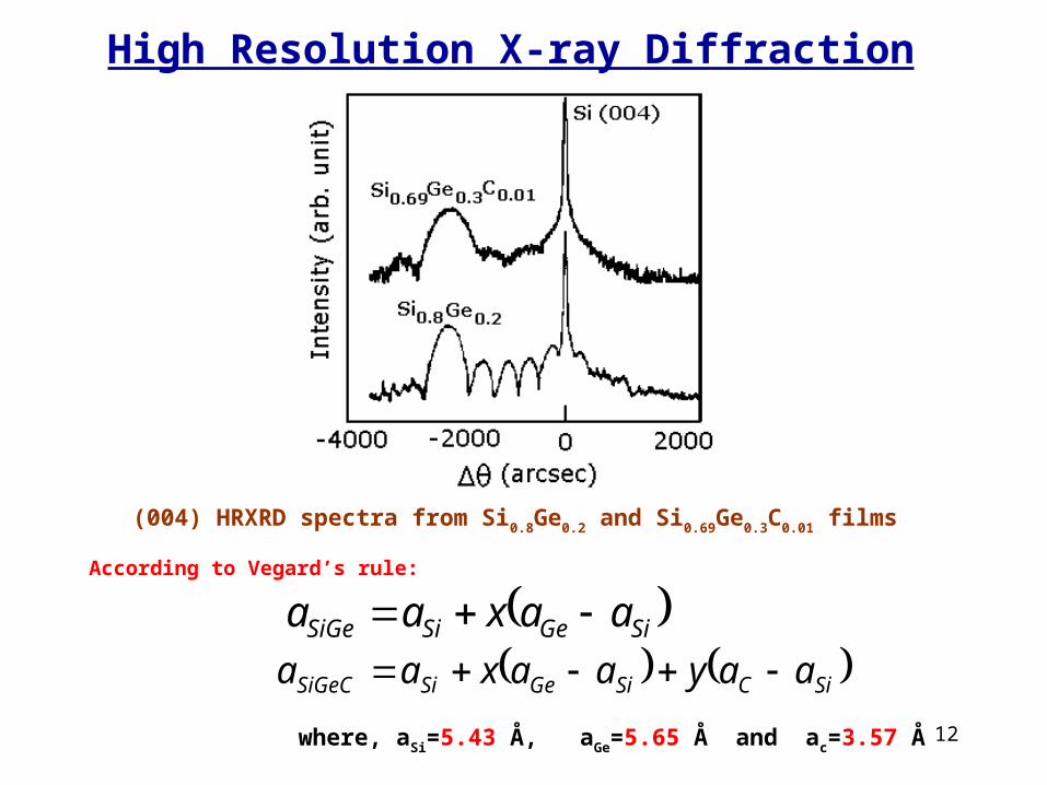
High Resolution X-ray Diffraction
(004) HRXRD spectra from Si0.8Ge0.2 and Si0.69Ge0.3C0.01 films
According to Vegard’s rule:
where, aSi=5.43 Å, aGe=5.65 Å and ac=3.57 Å
SiGeSiSiGe aaxaa SiCSiGeSiSiGeC aayaaxaa
13
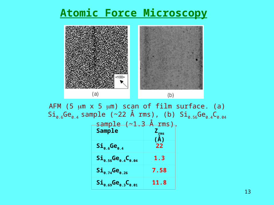
Atomic Force Microscopy
AFM (5 m x 5 m) scan of film surface. (a) Si0.6Ge0.4 sample (~22 Å
rms), (b) Si0.56Ge0.4C0.04 sample (~1.3 Å rms).
Sample Zrms (Å)
Si0.6Ge0.4 22
Si0.56Ge0.4C0.04 1.3
Si0.74Ge0.26 7.58
Si0.69Ge0.3C0.01 11.8
14
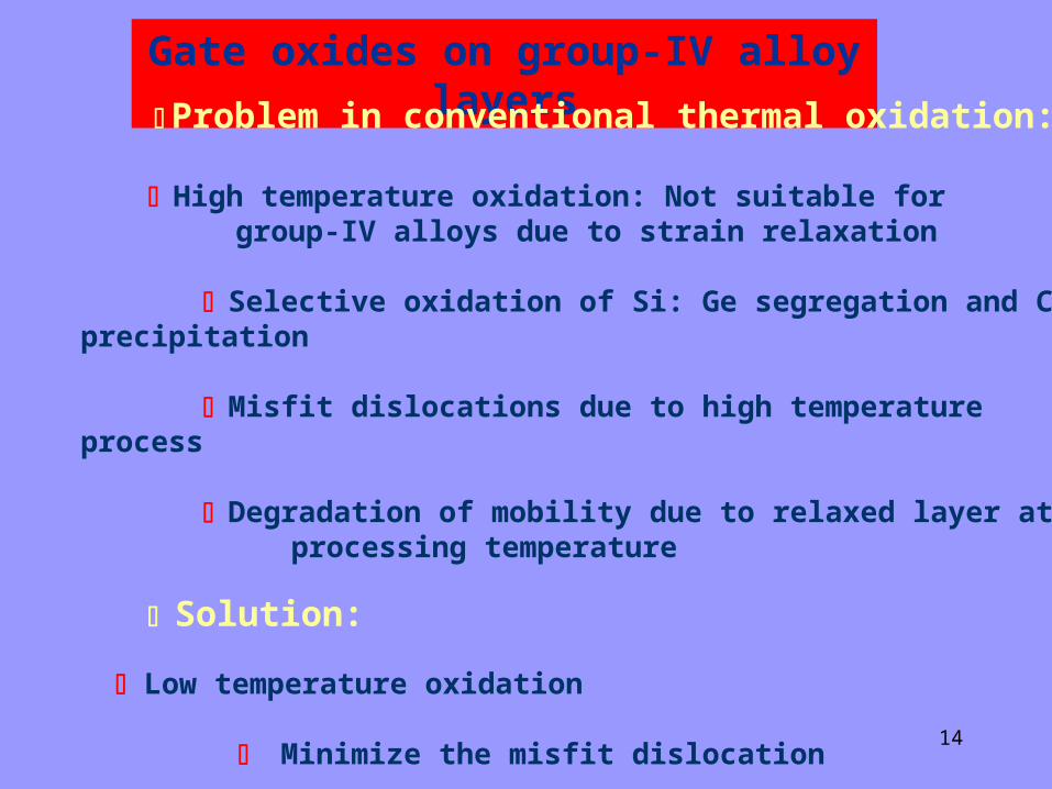
Gate oxides on group-IV alloy layers
Problem in conventional thermal oxidation: High temperature oxidation: Not suitable for group-IV alloys due to strain relaxation Selective oxidation of Si: Ge segregation and C precipitation Misfit dislocations due to high temperature process Degradation of mobility due to relaxed layer at processing temperature
Solution: Low temperature oxidation Minimize the misfit dislocation
15
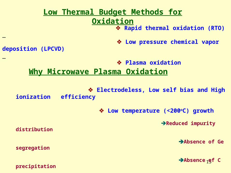
Low Thermal Budget Methods for Oxidation
Why Microwave Plasma Oxidation
Rapid thermal oxidation (RTO) Low pressure chemical vapor deposition (LPCVD) Plasma oxidation
Electrodeless, Low self bias and High ionization efficiency Low temperature (<200oC) growth Reduced impurity distribution
Absence of Ge segregation
Absence of C precipitation
16
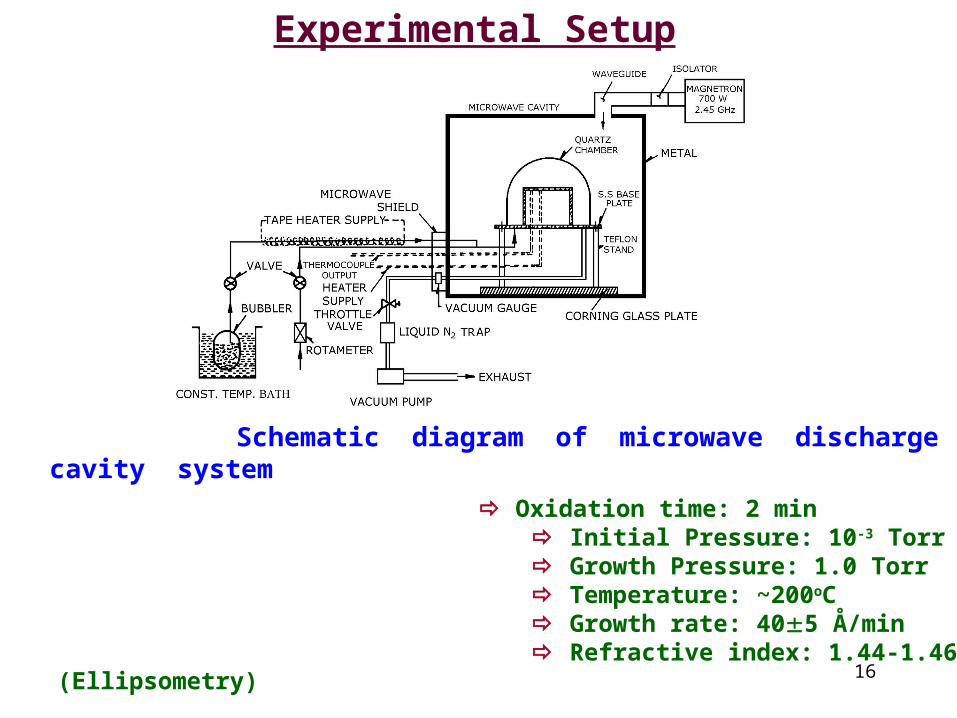
Experimental Setup
Schematic diagram of microwave discharge cavity system
Oxidation time: 2 min Initial Pressure: 10-3 Torr Growth Pressure: 1.0 Torr Temperature: ~200oC Growth rate: 405 Å/min Refractive index: 1.44-1.46 (Ellipsometry)
17
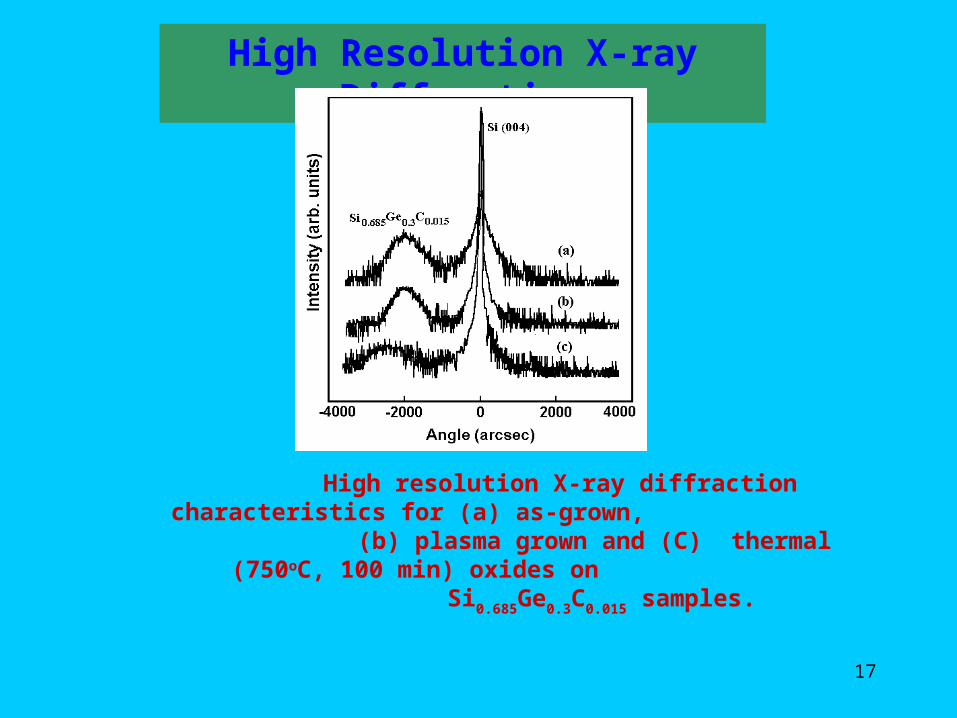
High Resolution X-ray Diffraction
High resolution X-ray diffraction characteristics for (a) as-grown, (b) plasma grown and (C) thermal (750oC, 100 min) oxides on
Si0.685Ge0.3C0.015 samples.
18
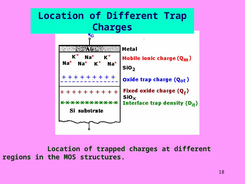
Location of Different Trap Charges
Location of trapped charges at different regions in the MOS structures.
19
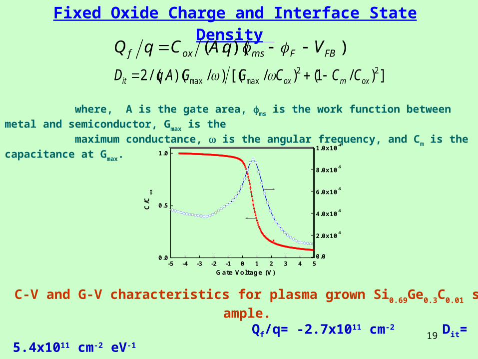
Fixed Oxide Charge and Interface State Density
))(.( FBFmsoxf VqACqQ
])/1()/[()/)(./(2 22maxmax oxmoxit CCCGGAqD
where, A is the gate area, ms is the work function between metal and semiconductor, Gmax is the
maximum conductance, is the angular frequency, and Cm is the capacitance at Gmax.
-5 -4 -3 -2 -1 0 1 2 3 4 50.0
0.5
1.0C
/C o
x
Gate Voltage (V)
0.0
2.0x10⁻⁵
4.0x10⁻⁵
6.0x10⁻⁵
8.0x10⁻⁵
1.0x10⁻⁴
C-V and G-V characteristics for plasma grown Si0.69Ge0.3C0.01 sample.
Qf/q= -2.7x1011 cm-2 Dit= 5.4x1011 cm-2 eV-1
20
Extraction of Material Parameters of SiGe/SiGeC Heterolayers
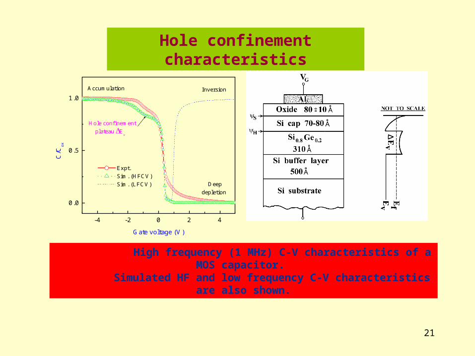
Hole confinement characteristics
Extraction of Si-cap layer thickness Extraction of buried and surface channel threshold voltages Determination of valence band offset: Si1-xGex and Si1-x-yGexCy heterolayers
Generation lifetime of group-IV alloy layers
21
-4 -2 0 2 4
0.0
0.5
1.0
Expt. Sim. (HFCV) Sim. (LFCV)
Hole confinement plateau E
v
Deep depletion
InversionAccumulation
C/C
ox
Gate voltage (V)
Hole confinement characteristics
High frequency (1 MHz) C-V characteristics of a MOS capacitor. Simulated HF and low frequency C-V characteristics are also shown.
22
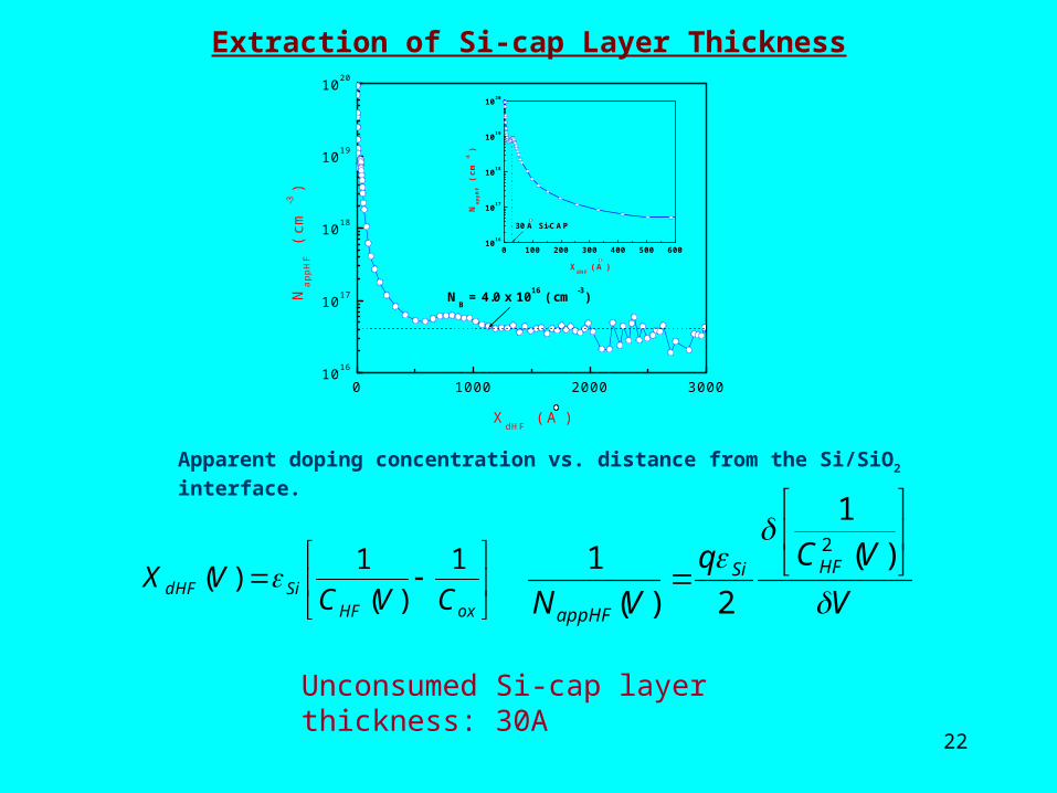
Extraction of Si-cap Layer Thickness
0 1000 2000 30001016
1017
1018
1019
1020
NB = 4.0 x 10¹⁶ ( cm -3)N
appH
F
( cm
-3 )
XdHF
( A )
0 100 200 300 400 500 6001016
1017
1018
1019
1020
30 A Si-CAP
Nap
pH
F (
cm
-3 )
XdHF
( A )
Apparent doping concentration vs. distance from the Si/SiO2 interface.
oxHFSidHF CVC
VX1
)(
1)(
V
VCq
VNHFSi
appHF
)(
1
2)(
12
Unconsumed Si-cap layer thickness: 30A
23
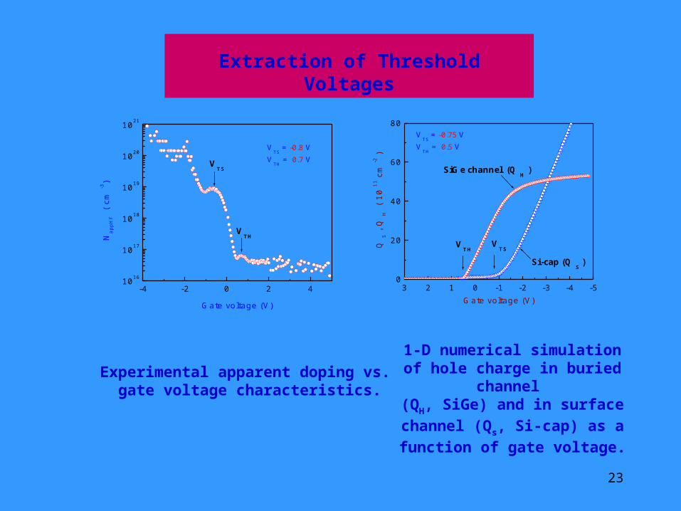
Extraction of Threshold Voltages
-4 -2 0 2 41016
1017
1018
1019
1020
1021
VTS
= -0.8 VV
TH = 0.7 V
VTH
VTS
Nap
pHF
( cm
-3)
Gate voltage (V)
Experimental apparent doping vs. gate voltage characteristics.
1-D numerical simulation of hole charge in buried channel
(QH, SiGe) and in surface channel
(Qs, Si-cap) as a function of gate
voltage.
3 2 1 0 -1 -2 -3 -4 -50
20
40
60
80V
TS = -0.75 V
VTH
= 0.5 V
(Q H )
(Q S )
SiGe channel
Si-cap
VTS
VTHQ
S ,
Q H
(
10
11 c
m -
2 )
Gate voltage (V)
24
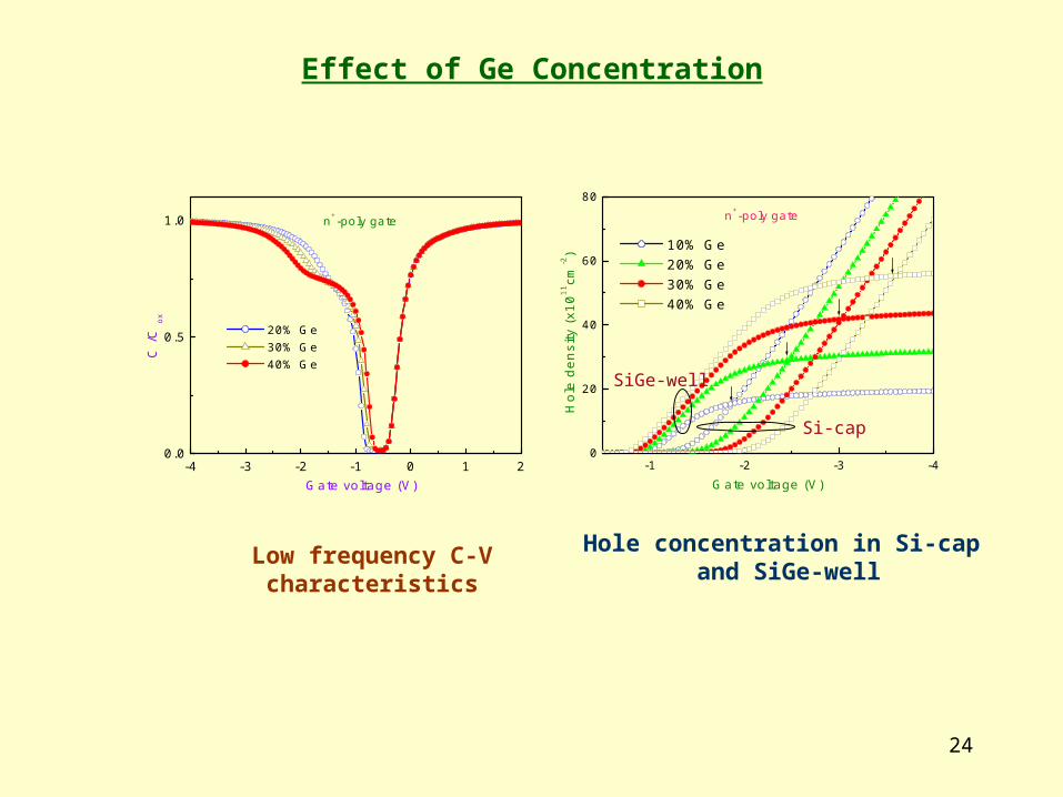
Effect of Ge Concentration
-4 -3 -2 -1 0 1 20.0
0.5
1.0 n+-poly gate
20% Ge 30% Ge 40% Ge
C /
C ox
Gate voltage (V)-1 -2 -3 -4
0
20
40
60
80n+-poly gate
10% Ge 20% Ge 30% Ge 40% Ge
Ho
le d
en
sity
(x1
011 cm
-2)
Gate voltage (V)
SiGe-well
Si-cap
Low frequency C-V characteristics Hole concentration in Si-cap and SiGe-well
25
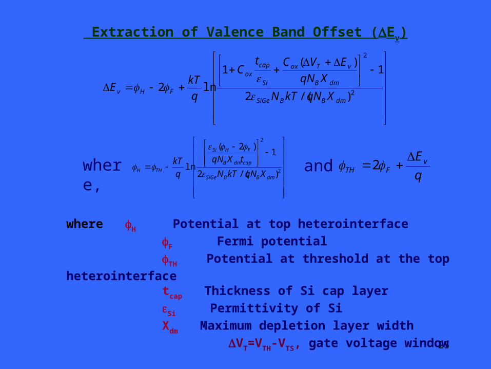
Extraction of Valence Band Offset (Ev)
2
2
)/(2
1)(
1
ln2dmBBSiGe
dmB
vTox
Si
capox
FHv XqNkTN
XqN
EVCtC
q
kTE
2
2
)/(2
1)2(
lndmBBSiGe
capdmB
FHSi
THH XqNkTN
tXqN
q
kT
q
EvFTH
2where, and
where H Potential at top heterointerface
F Fermi potential
TH Potential at threshold at the top heterointerface
tcap Thickness of Si cap layer
Si Permittivity of Si
Xdm Maximum depletion layer width
VT=VTH-VTS, gate voltage window
26
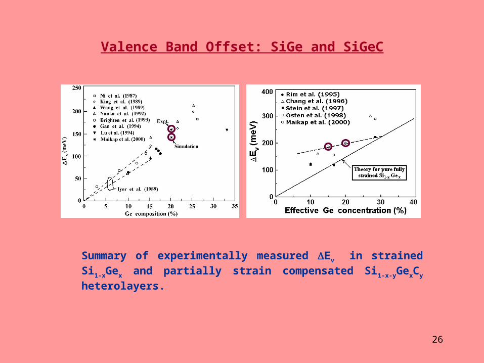
Valence Band Offset: SiGe and SiGeC
Summary of experimentally measured Ev in strained Si1-xGex and
partially strain compensated Si1-x-yGexCy heterolayers.
27
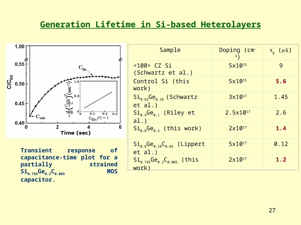
Generation Lifetime in Si-based Heterolayers
Sample Doping (cm-3) g (s)
<100> CZ Si (Schwartz et al.)
5x10¹⁵ 9
Control Si (this work) 5x10¹⁵ 5.6
Si0.82Ge0.18 (Schwartz et al.) 3x10¹⁷ 1.45
Si0.9Ge0.1 (Riley et al.) 2.5x10¹⁷ 2.6
Si0.8Ge0.2 (this work) 2x10¹⁷ 1.4
Si0.8Ge0.18C0.02 (Lippert et al.) 5x10¹⁷ 0.12
Si0.795Ge0.2C0.005 (this work) 2x10¹⁷ 1.2
Transient response of capacitance-time plot for a partially strained Si0.795Ge0.2C0.005
MOS capacitor.
28
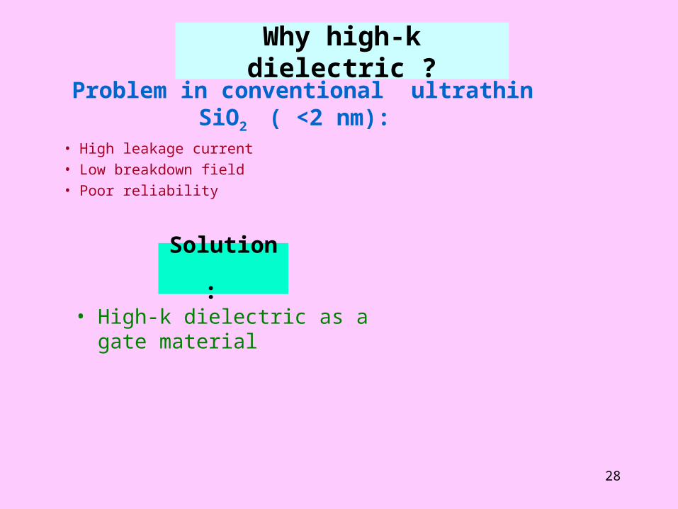
Why high-k dielectric ?
• High leakage current• Low breakdown field• Poor reliability
Problem in conventional ultrathin SiO2 ( <2 nm):
Solution: • High-k dielectric as a gate material
29
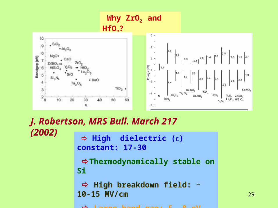
Why ZrO2 and HfO2?
High dielectric () constant: 17-30
Thermodynamically stable on Si
High breakdown field: ~ 10-15 MV/cm
Large band gap: 5 -8 eV
Low leakage current
J. Robertson, MRS Bull. March 217 (2002)
30
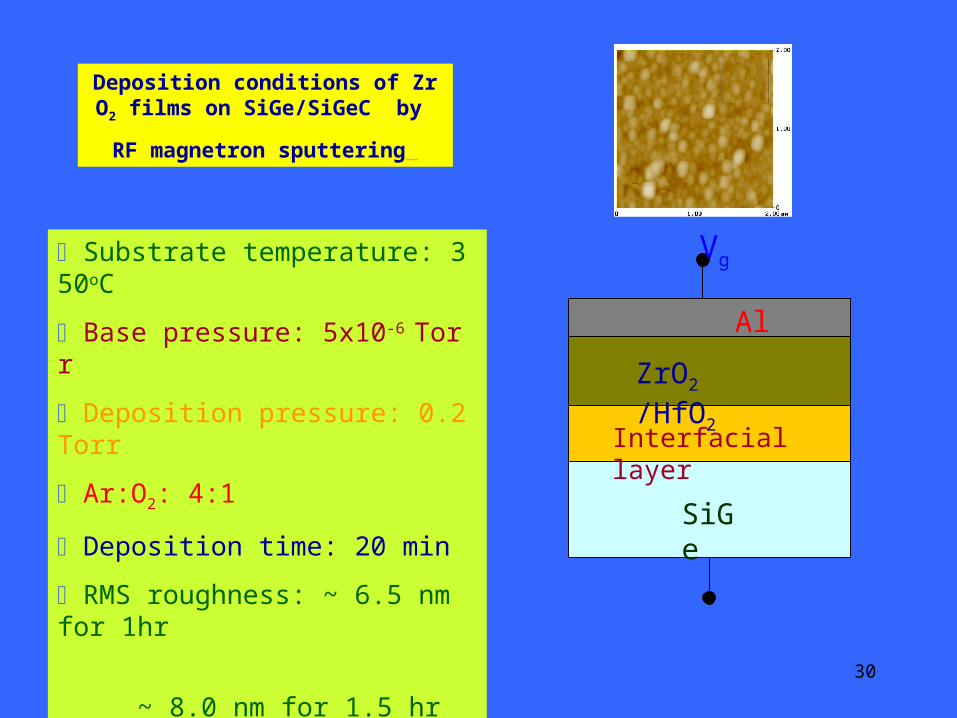
Deposition conditions of ZrO2 films on SiGe/SiGeC by
RF magnetron sputtering
Substrate temperature: 350oC
Base pressure: 5x10⁻⁶ Torr
Deposition pressure: 0.2 Torr
Ar:O2: 4:1
Deposition time: 20 min
RMS roughness: ~ 6.5 nm for 1hr
~ 8.0 nm for 1.5 hr SiGe
Vg
Al
ZrO2 /HfO2
Interfacial layer
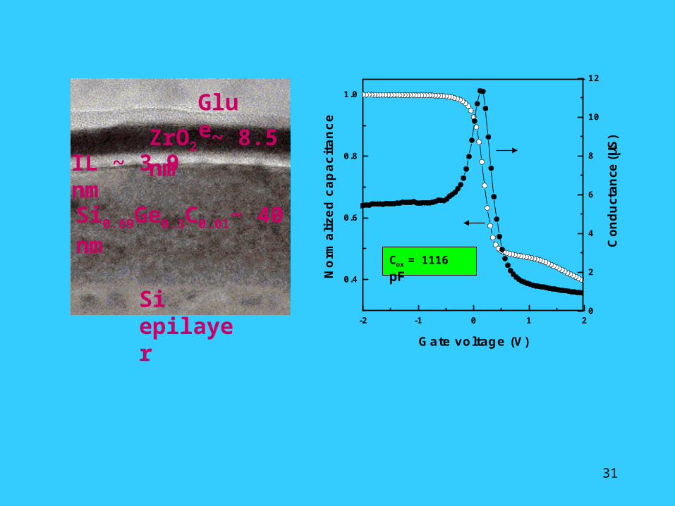
31
-2 -1 0 1 2
0.4
0.6
0.8
1.0
No
rmal
ized
cap
acit
ance
Gate voltage (V)
0
2
4
6
8
10
12
Con
duct
ance
(S
)
Cox = 1116 pF
Glue
ZrO2 ~ 8.5 nmIL ~ 3.9 nm
Si0.69Ge0.3C0.01~ 40 nm
Si epilayer
32
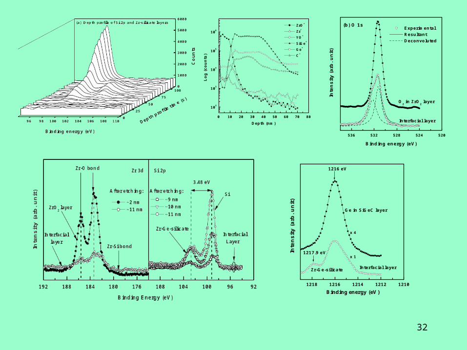
0 10 20 30 40 50 60 70 80
102
103
104
105
106
ZrO+
Zr+
YO+
SiGe+
Ge+
C+
Lo
g (
cou
nts
)
Depth (nm)
536 532 528 524 520
(b) O 1s
Inte
nsi
ty (
arb
. un
it)
Binding energy (eV)
Experimental Resultant Deconvoluted
O2 in ZrO
2 layer
Interfacial layer
1218 1216 1214 1212 1210
x 1
Inte
nsi
ty (
arb
. un
it)
x 4
Zr-Ge-silicate
1216 eV
1217.9 eV
Ge in SiGeC layer
Interfacial layer
Binding energy (eV)
33
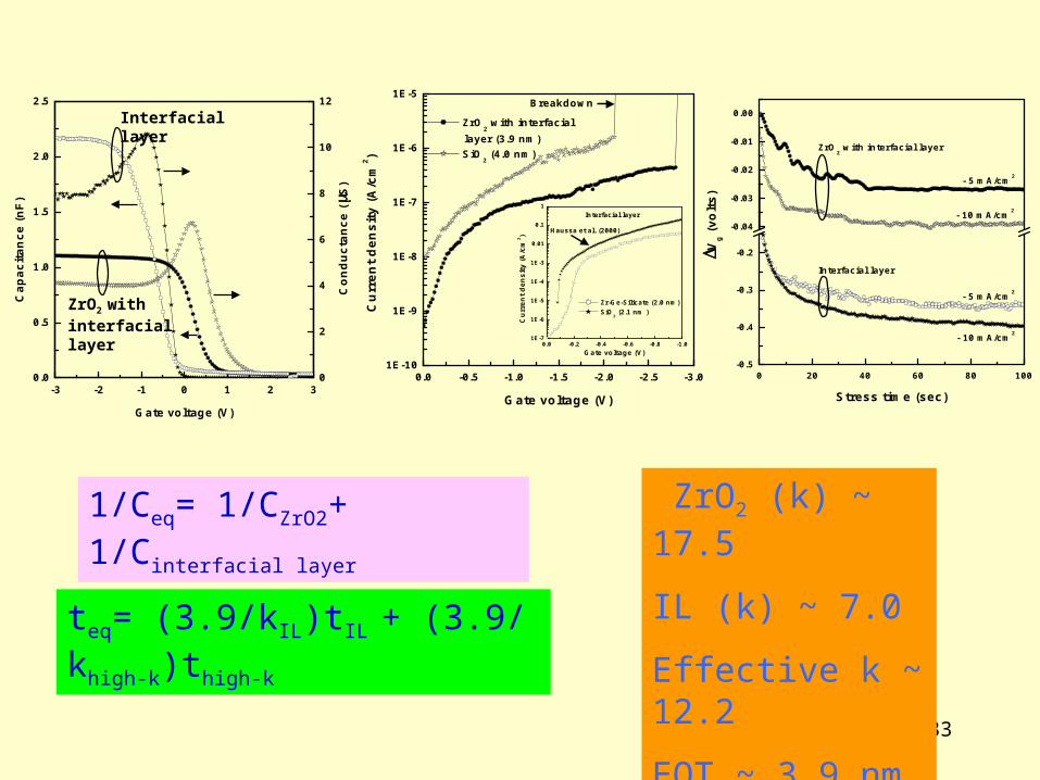
0
2
4
6
8
10
12
Co
nd
uct
ance
(S
)
-3 -2 -1 0 1 2 30.0
0.5
1.0
1.5
2.0
2.5
Cap
acit
ance
(n
F)
Gate voltage (V)
ZrO2 with interfacial layer
Interfacial layer
0.0 -0.5 -1.0 -1.5 -2.0 -2.5 -3.01E-10
1E-9
1E-8
1E-7
1E-6
1E-5Breakdown
ZrO2 with interfacial
layer (3.9 nm) SiO
2 (4.0 nm)
Cu
rren
t d
ensi
ty (
A/c
m2 )
Gate voltage (V)
0.0 -0.2 -0.4 -0.6 -0.8 -1.01E-7
1E-6
1E-5
1E-4
1E-3
0.01
0.1
1
Haussa et al. (2000)
Interfacial layer
Zr-Ge-Silicate (2.0 nm) SiO
2 (2.1 nm )
Cu
rren
t d
ensi
ty (
A/c
m2 )
Gate voltage (V)
1/Ceq= 1/CZrO2+ 1/Cinterfacial layer
teq= (3.9/kIL)tIL + (3.9/khigh-k)thigh-k
ZrO2 (k) ~ 17.5
IL (k) ~ 7.0
Effective k ~ 12.2
EOT ~ 3.9 nm
0 20 40 60 80 100-0.5
-0.4
-0.3
-0.2
-0.04
-0.03
-0.02
-0.01
0.00
- 5 mA/cm2
- 10 mA/cm2
- 10 mA/cm2
- 5 mA/cm2
Interfacial layer
ZrO2 with interfacial layer
Vg (
volt
s)
Stress time (sec)
34
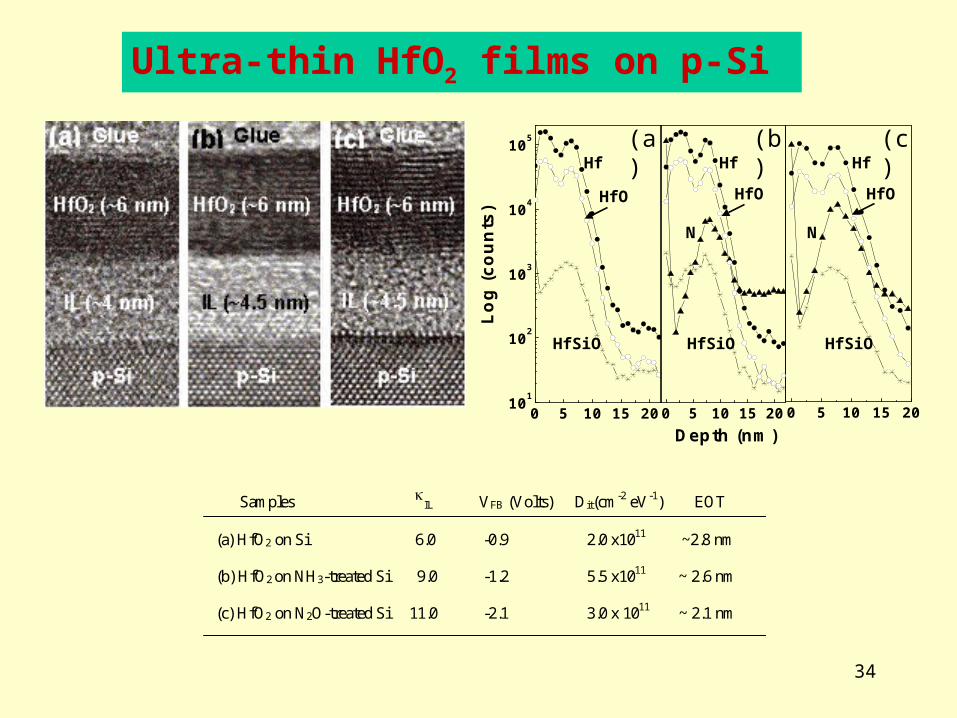
Ultra-thin HfO2 films on p-Si
0 5 10 15 20101
102
103
104
105
Lo
g (
cou
nts
)
0 5 10 15 20
0 5 10 15 20
Depth (nm)
(a) (b) (c)
HfSiO HfSiO HfSiO
HfO HfO HfO
Hf Hf Hf
N N
Samples IL VFB (Volts) Dit(cm-2 eV-1) EOT
(a) HfO2 on Si 6.0 -0.9 2.0 x10¹¹ ~2.8 nm
(b) HfO2 on NH3-treated Si 9.0 -1.2 5.5 x10¹¹ ~ 2.6 nm
(c) HfO2 on N2O-treated Si 11.0 -2.1 3.0 x 10¹¹ ~ 2.1 nm
35
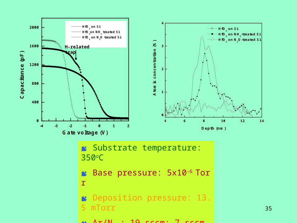
-4 -3 -2 -1 0 1 20
400
800
1200
1600
2000
HfO2 on Si
HfO2on NH
3 treated Si
HfO2 on N
2O treated Si
Cap
acit
ance
(p
F)
Gate voltage (V)
H-related trap
4 6 8 10 12 14
0
1
2
3
4 HfO
2 on Si
HfO2 on NH
3-treated Si
HfO2 on N
2O-treated Si
Ato
mic
co
nce
ntr
atio
n (
%)
Depth (nm)
Substrate temperature: 350oC
Base pressure: 5x10⁻⁶ Torr
Deposition pressure: 13.5 mTorr
Ar/N2 : 19 sccm: 7 sccm
Deposition time: 3 min
36
Conclusion
High quality strained Si1-xGex and partially strain
compensated Si1-x-yGexCy heterolayers: UHVCVD
Strained layer characterization: Composition and thickness of group-IV alloy layers: SIMS analysis
Crystalline quality: HRXRD study Surface roughness: AFM study
Low-temperature plasma oxidation: Preserve the strain in group-IV alloy layers
37
Extraction of material parameters for SiGe and SiGeC heterolayers: Threshold voltages of buried and surface channel, valence band offset, and carrier generation lifetime
ZrO2 and HfO2 high-k gate dielectrics Physical characterization: HRTEM, ToF-SIMS, XPS and AES measurements
Electrical characterization: C-V, G-V, I-V and gate voltage shift
38
Future scope
Annealing effect on ZrO2 and HfO2 high-k dielectrics on Si, SiGe, SiGeC and strained-Si heterolayers
Stacked gate dielectrics, NH3/HfO2 /N2O, on Si, SiGe, SiGeC and strained-Si heterolayers
39
Acknowledgments:
The author is grateful to Professor S. K. Banerjee, The University of Texas at Austin, for providing experimental support for the growth of strained Si1-xGex and Si1-x-yGexCy samples used in this study.
The author gratefully acknowledge financial support from the Creative Research Initiatives Program of the Korea Ministry of Science and Technology, South Korea