um10411 120 watt notebook adapter with tea1752t … information um10411 120 watt notebook adapter...
TRANSCRIPT

UM10411120 Watt notebook adapter with TEA1752T and TEA1791TRev. 1 — 19 October 2010 User manual
Document informationInfo ContentKeywords GreenChip-III, TEA1752T, GreenChip-SR, TEA1791T, PFC, flyback,
synchronous rectification, high efficiency, adapter, notebook, PC power
Abstract This manual provides the specification, performance, schematics, bill of materials and PCB layout of a 120 W notebook adapter using the TEA1752T and TEA1791T.
NXP Semiconductors UM10411120 Watt notebook adapter with TEA1752T and TEA1791T
Revision history Rev Date Description
v.1 20101019 First issue
UM10411 All information provided in this document is subject to legal disclaimers. © NXP B.V. 2010. All rights reserved.
User manual Rev. 1 — 19 October 2010 2 of 35
Contact informationFor more information, please visit: http://www.nxp.com
For sales office addresses, please send an email to: [email protected]

NXP Semiconductors UM10411120 Watt notebook adapter with TEA1752T and TEA1791T
1. Introduction
This manual describes a universal input, 19.5 V, 6.15 A single output power supply using TEA1752T and TEA1791T devices from the GreenChip-III and GreenChip Synchronous Rectification (SR) family of NXP Semiconductors. It contains the specification of the power supply, circuit diagram, the component list to build the supply, the PCB layout and component positions and documentation of the Power Factor Correction (PFC) choke and transformer, as well as test data and oscilloscope graphs of the most important waveforms. For design details on the TEA1752T and TEA1791T refer to the application note.
The GreenChip-III combines the control and drive for both the PFC and the flyback stages into a single device. The TEA1752T provides complete Switched Mode Power Supply (SMPS) control functionality in compliance with IEC61000-3-2 harmonic current emission requirements, a significant reduction of components, saving PCB space and providing a cost benefit. It also offers extremely low power consumption in no-load mode which makes it suitable for the low power consumer markets. The built-in green functions ensure high efficiency at all power levels, which results in a design that can easily meet all existing and proposed energy efficiency standards such as: European Union Code of Conduct (CoC), ENERGY STAR (US), California Energy Commission (CEC), Minimum Performance Energy Standards (MEPS) (Australian and New Zealand) and China Energy Conservation Program (CECP).
The GreenChip-SR is a synchronous rectification control IC that needs no external components to tune the timing. Used in notebook adapter designs, the GreenChip-SR offers a wide VCC operating range between 8.5 V and 38 V, minimizing the number of external components required and enabling simpler designs. In addition, the high driver output voltage (10 V) makes the GreenChip-SR compatible with all brands of MOSFETs.
WARNING
Lethal voltage and fire ignition hazard
The non-insulated high voltages that are present when operating this product, constitute a risk of electric shock, personal injury, death and/or ignition of fire. This product is intended for evaluation purposes only. It shall be operated in a designated test area by personnel qualified according to local requirements and labor laws to work with non-insulated mains voltages and high-voltage circuits. This product shall never be operated unattended.
UM10411 All information provided in this document is subject to legal disclaimers. © NXP B.V. 2010. All rights reserved.
User manual Rev. 1 — 19 October 2010 3 of 35
NXP Semiconductors UM10411120 Watt notebook adapter with TEA1752T and TEA1791T
2. Specification
• Mains input voltage: 90 V to 264 V; 47 Hz to 63 Hz• DC output: 19.5 V; ±2 %• Maximum continuous output current: 6.15 A• Peak output current: ≥ 7.6 A• Efficiency: ≥ 87 % at maximum load• ENERGY STAR active mode efficiency: > 89.5 %• No load power consumption: ≤ 0.25 W• Dynamic load response (peak-to-peak): 700 mV• Output ripple and noise (peak-to-peak): 100 mV• CISPR22 class B conducted ElectroMagnetic Interference (EMI) (Pass)• EN61000-4-2 immunity against ElectroStatic Discharge (ESD) (≥ 12 kV air discharge)• EN61000-3-2 A14 (harmonics) compliance• Short-circuit Protection (SCP); input power < 1.2 W during SCP test• OverCurrent Protection (OCP); input power < 2.2 W during OCP test• Latched output OverVoltage Protection (OVP): < 24 V• Latched OverTemperature Protection (OTP); ≤ 120 °C• Fast Latch Reset (FLR): < 2 s
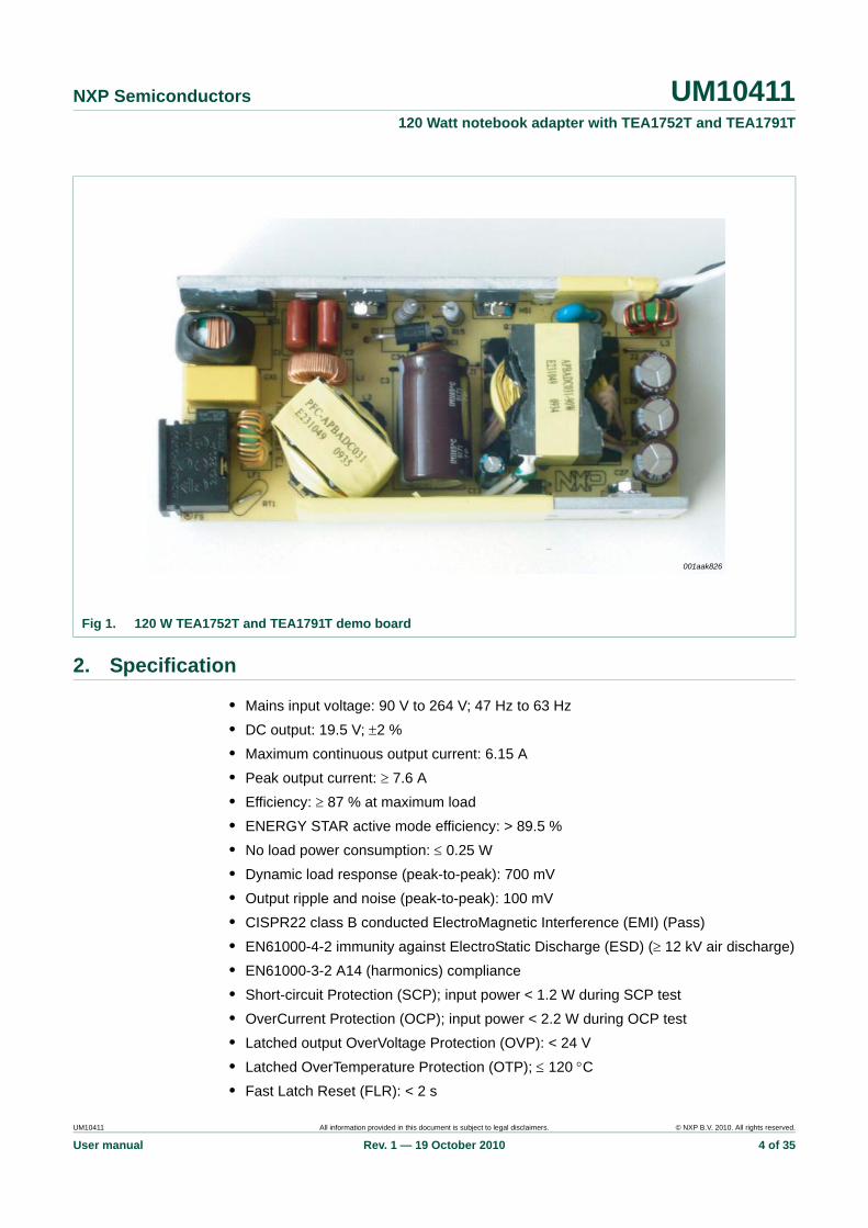
Fig 1. 120 W TEA1752T and TEA1791T demo board
001aak826
UM10411 All information provided in this document is subject to legal disclaimers. © NXP B.V. 2010. All rights reserved.
User manual Rev. 1 — 19 October 2010 4 of 35
NXP Semiconductors UM10411120 Watt notebook adapter with TEA1752T and TEA1791T
3. Performance data
3.1 Test setup
3.1.1 Test equipment
• AC source: Agilent 6812B• Power meter: Yokogawa WT210 with harmonics option• DC electronic load: Chroma, Model 63103• Digital oscilloscope: Yokogawa DL1640L
• Current probe Yokogawa 701933 30A; 50 MHz• 100 MHz, high voltage differential probe: Yokogawa 700924• 500 MHz, low voltage differential probe: Yokogawa 701920• Multimeter: Keithley 2000• ElectroMagnetic Compatibility (EMC) receiver: Rohde and Schwarz ESPI-3 + Line
Impedance Standardization Network (LISN) ENV216
3.1.2 Test conditions
• Adapter on the lab-table with heat sinks facing downwards• The adapter has no casing• Ambient temperature between 20 °C and 25 °C• Measurements were made after stabilization of temperature according to "test method
for calculating the efficiency of single-voltage external AC-to-DC and AC-to-AC power supplies" of ENERGY STAR
3.2 Efficiency
3.2.1 ENERGY STAR efficiencyTo market adapters as ENERGY STAR efficient they must pass the active mode and no-load criteria as stated in the ENERGY STAR standard for External Power Supplies; EPS2.0. The minimum active-mode efficiency is defined as the arithmetic average efficiency at 25 %, 50 %, 75 % and 100 % of the rated output power as printed on the nameplate of the adapter.
3.2.1.1 Active mode efficiencyTest conditions:
The adapter is set to maximum load and preheated until temperature stabilization is achieved. Temperature stabilization is established for every load step before recording any measurements.
Remark: The output voltage is measured at the end of the output cable (2 × 20 mΩ).
UM10411 All information provided in this document is subject to legal disclaimers. © NXP B.V. 2010. All rights reserved.
User manual Rev. 1 — 19 October 2010 5 of 35
NXP Semiconductors UM10411120 Watt notebook adapter with TEA1752T and TEA1791T
Pass criteria:
To comply with ENERGY STAR EPS2.0, the arithmetic average of the four efficiency measurements must be ≥ 87 %. Universal mains adapters must pass the criteria at both 115 V; 60 Hz and 230 V; 50 Hz. To meet this criteria, the PFC must be off at 25 % load and preferably on at 50 % load.
3.2.1.2 No-load input powerTest conditions:
The adapter is set to maximum load and preheated. After five minutes the load is removed. The no-load input power measurements were recorded after stabilization of the input power reading.
Pass criteria:
To comply with ENERGY STAR EPS2.0, the input power must be less than 0.5 W. Universal mains adapters must pass the criteria at both 115 V; 60 Hz and 230 V; 50 Hz.
The adapter is set to maximum load and preheated. After five minutes the load is removed. The no-load input power measurements were recorded after stabilization of the input power reading.
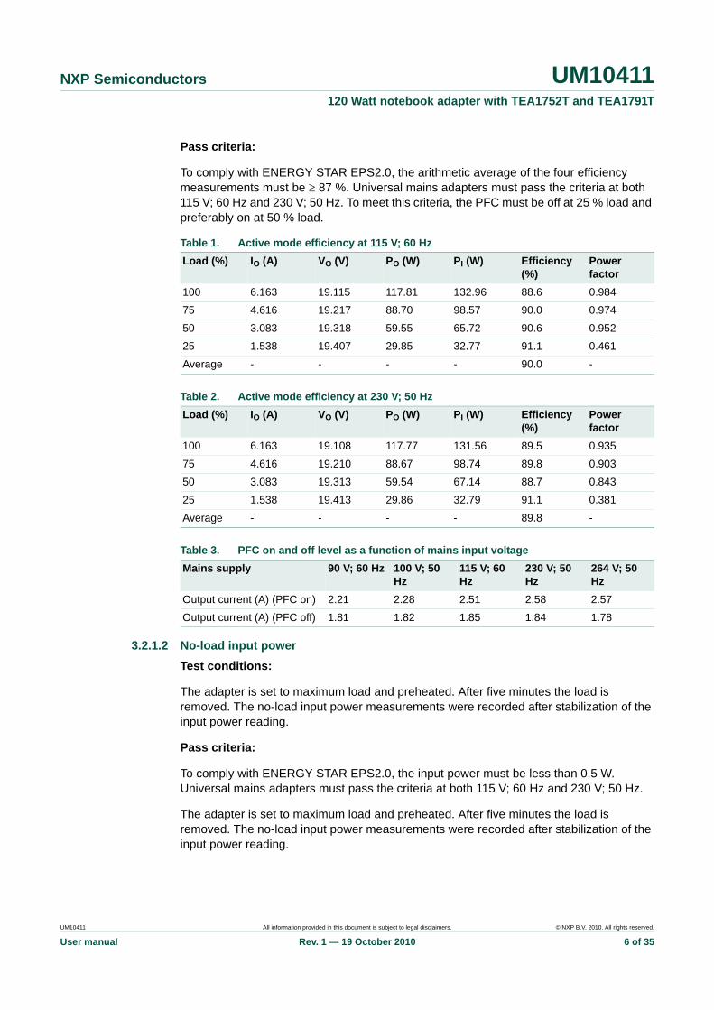
Table 1. Active mode efficiency at 115 V; 60 Hz Load (%) IO (A) VO (V) PO (W) PI (W) Efficiency
(%)Power factor
100 6.163 19.115 117.81 132.96 88.6 0.984
75 4.616 19.217 88.70 98.57 90.0 0.974
50 3.083 19.318 59.55 65.72 90.6 0.952
25 1.538 19.407 29.85 32.77 91.1 0.461
Average - - - - 90.0 -
Table 2. Active mode efficiency at 230 V; 50 Hz Load (%) IO (A) VO (V) PO (W) PI (W) Efficiency
(%)Power factor
100 6.163 19.108 117.77 131.56 89.5 0.935
75 4.616 19.210 88.67 98.74 89.8 0.903
50 3.083 19.313 59.54 67.14 88.7 0.843
25 1.538 19.413 29.86 32.79 91.1 0.381
Average - - - - 89.8 -
Table 3. PFC on and off level as a function of mains input voltage Mains supply 90 V; 60 Hz 100 V; 50
Hz115 V; 60 Hz
230 V; 50 Hz
264 V; 50 Hz
Output current (A) (PFC on) 2.21 2.28 2.51 2.58 2.57
Output current (A) (PFC off) 1.81 1.82 1.85 1.84 1.78
UM10411 All information provided in this document is subject to legal disclaimers. © NXP B.V. 2010. All rights reserved.
User manual Rev. 1 — 19 October 2010 6 of 35

NXP Semiconductors UM10411120 Watt notebook adapter with TEA1752T and TEA1791T
3.2.1.3 Full load efficiency PFC plus flyback stageTest conditions:
Before any measurements were recorded, the adapter is set to maximum load and is preheated until the readings were stabilized.
Remark: The output voltage is measured at the end of the output cable. (2 × 20 mΩ)
Pass criteria:
The efficiency (η) must be ≥ 87 % at the maximum continuous output load.
3.3 Timing and protection
3.3.1 Switch-on delay and output rise timeTest conditions:
The electronic load is set to Constant Current (CC) mode and Von = 0 V. The electronic load is set to the maximum continuous output current.
Pass criteria:
• Switch-on delay: 2 seconds maximum from application of the AC mains voltage is applied to the time when the output is within regulation
• Output rise time: The output voltage must rise from 10 % of the maximum to the regulation limit within 30 ms. There must be a smooth and continuous ramp-up of the output voltage. No voltage with a negative polarity must be present at the output during start-up
• No output bounce or error is allowed during switch-on• There be must be sufficient margin between the FBCTRL signal and the 4.5 V
time-out trigger level to avoid false triggering of the time-out protection due to component tolerances
Table 4. No-load input power No-load input power as a function of the mains input voltage.
Mains supply 90 V; 60 Hz 100 V; 50 Hz 115 V; 60 Hz 230 V; 50 Hz 264 V; 50 HzInput power PI (W) 0.135 0.139 0.143 0.210 0.240
Table 5. PFC plus flyback stage Total converter efficiency (at full load) as a function of the mains input
Mains supply II RMS (A) PO (W) PI (W) Efficiency (%)
Power factor
(V) (Hz)90 60 1.52 117.71 135.07 87.1 0.989
100 50 1.35 117.78 134.09 87.8 0.987
115 60 1.17 117.81 132.96 88.6 0.984
230 50 0.61 117.77 131.56 89.5 0.935
264 50 0.54 117.81 131.36 89.7 0.917
UM10411 All information provided in this document is subject to legal disclaimers. © NXP B.V. 2010. All rights reserved.
User manual Rev. 1 — 19 October 2010 7 of 35

NXP Semiconductors UM10411120 Watt notebook adapter with TEA1752T and TEA1791T
a. Mains input 90 V; 60 Hz; delay time 484 ms b. Mains input 264 V; 50 Hz; delay time 484 ms
Load = 6.15 ACH1: mains inputCH2: pin VCC TEA1752TCH3: pin FBCTRL TEA1752TCH4: output voltage
Load = 6.15 ACH1: mains inputCH2: pin VCC TEA1752TCH3: pin FBCTRL TEA1752TCH4: output voltage
Fig 2. Delay between switch-on and output in regulation
019aaa011 019aaa012
a. Mains input 90 V; 60 Hz; output rise time 12.64 ms b. Mains input 264 V; 50 Hz; output rise time 12.24 ms
Load = 6.15 ACH1: mains inputCH2: pin FBCTRL TEA1752TCH3: pin FBSENSE TEA1752T (soft start)CH4: output voltage
Load = 6.15 ACH1: mains inputCH2: pin VCC TEA1751TCH3: pin FBSENSE TEA1751T (soft start)CH4: output voltage
Fig 3. Output rise time at full load start-up
019aaa009 019aaa010
UM10411 All information provided in this document is subject to legal disclaimers. © NXP B.V. 2010. All rights reserved.
User manual Rev. 1 — 19 October 2010 8 of 35
NXP Semiconductors UM10411120 Watt notebook adapter with TEA1752T and TEA1791T
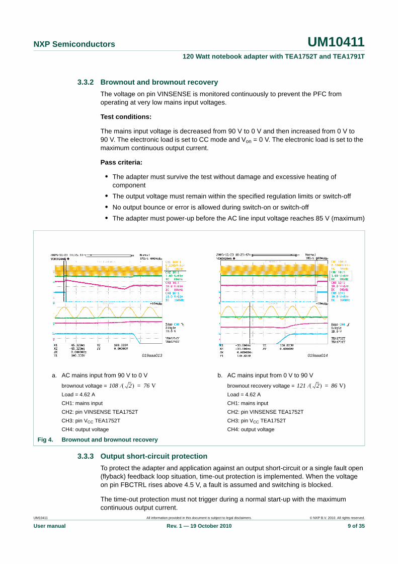
3.3.2 Brownout and brownout recoveryThe voltage on pin VINSENSE is monitored continuously to prevent the PFC from operating at very low mains input voltages.
Test conditions:
The mains input voltage is decreased from 90 V to 0 V and then increased from 0 V to 90 V. The electronic load is set to CC mode and Von = 0 V. The electronic load is set to the maximum continuous output current.
Pass criteria:
• The adapter must survive the test without damage and excessive heating of component
• The output voltage must remain within the specified regulation limits or switch-off• No output bounce or error is allowed during switch-on or switch-off• The adapter must power-up before the AC line input voltage reaches 85 V (maximum)
3.3.3 Output short-circuit protectionTo protect the adapter and application against an output short-circuit or a single fault open (flyback) feedback loop situation, time-out protection is implemented. When the voltage on pin FBCTRL rises above 4.5 V, a fault is assumed and switching is blocked.
The time-out protection must not trigger during a normal start-up with the maximum continuous output current.
a. AC mains input from 90 V to 0 V b. AC mains input from 0 V to 90 V
brownout voltage = Load = 4.62 ACH1: mains inputCH2: pin VINSENSE TEA1752TCH3: pin VCC TEA1752TCH4: output voltage
brownout recovery voltage = Load = 4.62 ACH1: mains inputCH2: pin VINSENSE TEA1752TCH3: pin VCC TEA1752TCH4: output voltage
Fig 4. Brownout and brownout recovery
019aaa013 019aaa014
108 2( )⁄ 76 V= 121 2( )⁄ 86 V)=
UM10411 All information provided in this document is subject to legal disclaimers. © NXP B.V. 2010. All rights reserved.
User manual Rev. 1 — 19 October 2010 9 of 35

NXP Semiconductors UM10411120 Watt notebook adapter with TEA1752T and TEA1791T
Test conditions:
There are two test conditions:
1. The adapter is switched on with 6.15 A output load. After start-up a short-circuit is applied manually at the end of the output cable
2. Before the adapter is switched on a short-circuit is applied to the end of the output cable
Remark: An output short-circuit is defined as an output impedance of less than 0.1 Ω.
Pass criteria:
• The adapter must be capable of withstanding a continuous short-circuit at the output without damaging or overstressing the adapter under any input conditions
• The average input power must be less than 3 W during the short-circuit test• The adapter must automatically recover after removal of the short-circuit
a. Mains input 90 V; 60 Hz b. Mains input 264 V; 50 Hz
Load before short-circuit = 6.15 ACH1: drain flyback MOSFETCH2: pin FBCTRL TEA1752TCH3: pin VCC TEA1752TCH4: output voltage
Load before short-circuit = 6.15 ACH1: drain flyback MOSFETCH2: pin FBCTRL TEA1752TCH3: pin FBDRIVER TEA1752TCH4: output voltage
Fig 5. Output short-circuit, triggering of the time-out protection
019aaa015 019aaa016
UM10411 All information provided in this document is subject to legal disclaimers. © NXP B.V. 2010. All rights reserved.
User manual Rev. 1 — 19 October 2010 10 of 35

NXP Semiconductors UM10411120 Watt notebook adapter with TEA1752T and TEA1791T
a. Output short-circuit during normal operation b. Output short-circuit applied before start-up
Load before short-circuit = 6.15 ACH1: drain flyback MOSFETCH2: pin FBCTRL TEA1752TCH3: pin VCC TEA1752TCH4: output voltage
Load = short-circuitCH1: drain flyback MOSFETCH2: pin FBCTRL TEA1752TCH3: pin VCC TEA1752TCH4: output voltage
Fig 6. Output short-circuit at 90 V; 60 Hz
019aaa017019aaa018
a. Output short-circuit during normal operation b. Output short-circuit applied before start-up
Load before short-circuit = 6.15 ACH1: drain flyback MOSFETCH2: pin FBCTRL TEA1752TCH3: pin VCC TEA1752TCH4: output voltage
Load = short-circuitCH1: drain flyback MOSFETCH2: pin FBCTRL TEA1752TCH3: pin VCC TEA1752TCH4: output voltage
Fig 7. Output short-circuit at 264 V; 50 Hz
019aaa019019aaa020
UM10411 All information provided in this document is subject to legal disclaimers. © NXP B.V. 2010. All rights reserved.
User manual Rev. 1 — 19 October 2010 11 of 35

NXP Semiconductors UM10411120 Watt notebook adapter with TEA1752T and TEA1791T
3.3.4 Output OverCurrent protectionTest conditions:
• The electronic load is set in CC mode• The load is increased from the maximum continuous value in small steps until the
OCP is triggered. The input power is measured after triggering over the OCP without changing the load setting
Pass criteria:
• The output power must be limited to less than 150 W, just before the triggering of the OCP
• The average input power must be less than 3 W once the OCP has been triggered
3.3.5 Output OverVoltage protectionTest conditions:
• The adapter is switched on without a load at the output• An output over-voltage is created by applying a short-circuit across the opto LED of
U2
Pass criteria:
• The output voltage must not exceed 25 V or stabilize between 25 V and the rated output voltage
• The voltage on TEA1752T pin VCC must not exceed the absolute maximum rating of 38 V
• When OVP is triggered, the primary side controller must shutdown and stay in a latched mode
• A single point fault must not cause a sustained overvoltage condition at the output
Table 6. Output short-circuit input power Output short-circuit input power as a function of the mains input voltage
Mains supply 90 V; 60 Hz 100 V; 50 Hz 115 V; 60 Hz 230 V; 50 Hz 264 V; 50 HzInput power PI (W) 1.81 1.75 1.71 1.56 1.05
Table 7. Output OCP and input power as a function of the mains input voltage Mains supply 90 V; 60 Hz 100 V; 50 Hz 115 V; 60 Hz 230 V; 50 Hz 264 V; 50 HzOCP (A) 7.9 7.9 7.9 7.5 7.5
Input power PI (W) 2.3 2.2 2.2 2.2 1.1
Table 8. Output OVP Output over-voltage at no-load as a function of the mains input voltage with protection mode latched
Mains supply 90 V; 60 Hz 100 V; 50 Hz
115 V; 60 Hz
230 V; 50 Hz
264 V; 50 Hz
Output OVP trip point (V) 23.4 23.4 23.2 23.3 23.3
VCC maximum during OVP (V)
27.2 27.2 27.1 27.0 27.0
UM10411 All information provided in this document is subject to legal disclaimers. © NXP B.V. 2010. All rights reserved.
User manual Rev. 1 — 19 October 2010 12 of 35

NXP Semiconductors UM10411120 Watt notebook adapter with TEA1752T and TEA1791T
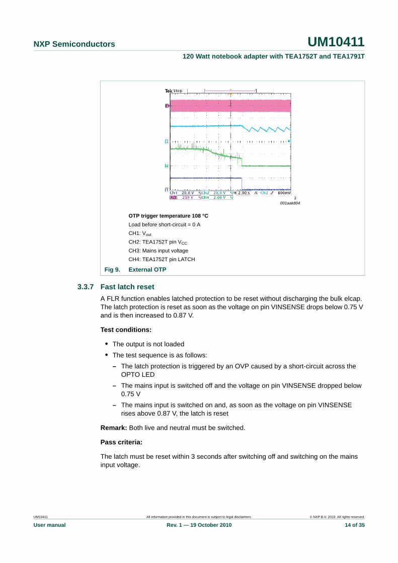
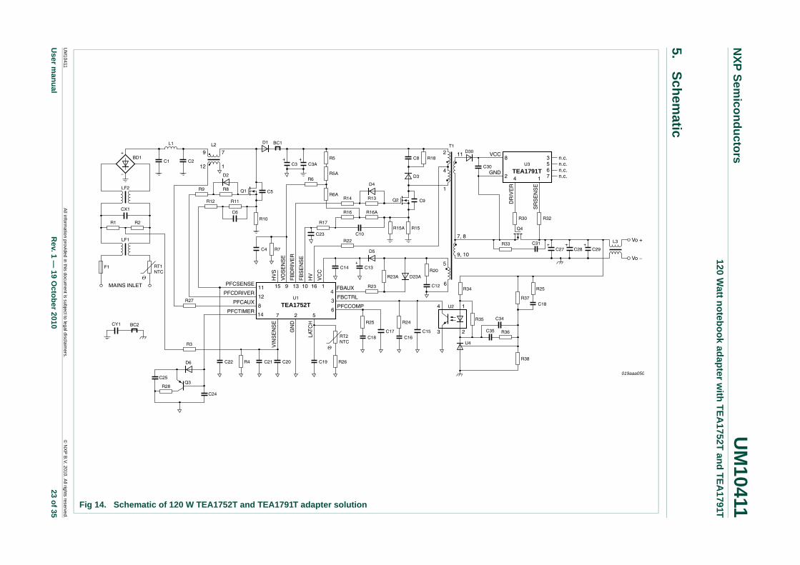
3.3.6 OverTemperature protectionAn accurate external OTP (TEA1752T pin LATCH, RT2, R26 and C19) is provided on the demo board to protect the flyback transformer against overheating (see Figure 14). Normally, the flyback transformer is the most heat sensitive component.
Test conditions:
The NTC temperature sensor glued to the transformer, is heated using a heat gun.
Pass criteria:
The IC must latch off the output at a VLATCH trip level of 1.25 V. No output bounce or error is allowed.
a. Mains input 90 V; 60 Hz b. Mains input 264 V; 50 Hz
Load before short-circuit = 0 ACH1: drain flyback MOSFETCH2: pin FBCTRL TEA1752TCH3: pin VCC TEA1752TCH4: output voltage
Load before short-circuit = 0 ACH1: drain flyback MOSFETCH2: pin FBCTRL TEA1752TCH3: pin VCC TEA1752TCH4: output voltage
Fig 8. Output OVP
019aaa021 019aaa022
UM10411 All information provided in this document is subject to legal disclaimers. © NXP B.V. 2010. All rights reserved.
User manual Rev. 1 — 19 October 2010 13 of 35
NXP Semiconductors UM10411120 Watt notebook adapter with TEA1752T and TEA1791T
3.3.7 Fast latch resetA FLR function enables latched protection to be reset without discharging the bulk elcap. The latch protection is reset as soon as the voltage on pin VINSENSE drops below 0.75 V and is then increased to 0.87 V.
Test conditions:
• The output is not loaded• The test sequence is as follows:
– The latch protection is triggered by an OVP caused by a short-circuit across the OPTO LED
– The mains input is switched off and the voltage on pin VINSENSE dropped below 0.75 V
– The mains input is switched on and, as soon as the voltage on pin VINSENSE rises above 0.87 V, the latch is reset
Remark: Both live and neutral must be switched.
Pass criteria:
The latch must be reset within 3 seconds after switching off and switching on the mains input voltage.
OTP trigger temperature 108 °CLoad before short-circuit = 0 ACH1: Vout
CH2: TEA1752T pin VCC
CH3: Mains input voltageCH4: TEA1752T pin LATCH
Fig 9. External OTP
001aak804
UM10411 All information provided in this document is subject to legal disclaimers. © NXP B.V. 2010. All rights reserved.
User manual Rev. 1 — 19 October 2010 14 of 35

NXP Semiconductors UM10411120 Watt notebook adapter with TEA1752T and TEA1791T
3.4 Output regulation and characterization
3.4.1 Load regulationTest conditions:
• The output voltage deviation is measured while the load current on the output is increased from 0 A to 6.15 A
• The measurement is repeated for different mains input voltages
Remark: The output voltage is measured at the end of the output cable (2 × 20 mΩ).
Pass criteria:
The output load regulation must remain within 2 %.
The load regulation is calculated using Equation 1.
(1)
where VO(nom) = 19.5 V.
a. Mains input 90 V; 60 Hz; FLR = 1.6 s b. Mains input 264 V; 50 Hz; FLR = 1.3 s
CH1: Vout
CH2: pin VCC TEA1752TCH3: AC mains inputCH4: pin VINSENSE TEA1752T
CH1: Vout
CH2: pin VCC TEA1752TCH3: AC mains inputCH4: pin VINSENSE TEA1752T
Fig 10. Fast latch reset
001aak805 001aak806
Table 9. Load regulation Output voltage as a function of the output load and the mains input voltage
Mains supply 90 V; 60 Hz 90 V; 60 Hz 264 V; 50 Hz 264 V; 50 HzVO; IO (V; A) 19.160; 6.15 19.470; 0 19.165; 6.15 19.471; 0
VO max( ) VO min( )–VO nom( )
------------------------------------------- 100 %×
UM10411 All information provided in this document is subject to legal disclaimers. © NXP B.V. 2010. All rights reserved.
User manual Rev. 1 — 19 October 2010 15 of 35
NXP Semiconductors UM10411120 Watt notebook adapter with TEA1752T and TEA1791T
Load regulation at 90 V; 60 Hz is calculated as follows:
(2)
Load regulation at 264 V; 50 Hz is calculated as follows:
(3)
3.4.2 Line regulationTest conditions:
• The output voltage deviation is measured while the mains voltage on the input is increased from 90 V to 264 V
• The measurement is repeated for different mains input voltages
Remark: The output voltage is measured at the end of the output cable. The load current is 6.15 A.
The line regulation is calculated using the following equation:
(4)
Pass criteria:
The output voltage deviation must remain within 0.05 %.
Load regulation at 90 V; 60 Hz is calculated using the following equation:
(5)
3.4.3 Ripple and noise periodic and random deviationRipple and noise are defined as the periodic or random signals over a frequency band of 10 Hz to 20 MHz.
Test conditions:
• The measurement is made with an oscilloscope set to a bandwidth of 20 MHz• The output is shunted at the end of the output cable by a 0.1 μF ceramic disk
capacitor and a 22 μF electrolytic capacitor to simulate loading
Pass criteria:
The output ripple and noise must remain within the specified limits 100 mV (peak-to-peak) at a maximum load current of 6.15 A.
19.470V 19.160V–19.5V
----------------------------------------------- 100 %× 1.6 %=
19.471V 19.165V–19.5V
----------------------------------------------- 100 %× 1.6 %=
Table 10. Line regulation Output voltage (at full load) as a function of the mains input voltage
Mains supply 90 V; 60 Hz 100 V; 50 Hz 115 V; 60 Hz 230 V; 50 Hz 264 V; 50 HzVO (V) 19.147 19.147 19.147 19.148 19.148
VO max( ) VO min( )–VO nom( )
------------------------------------------- 100 %×
19.148V 19.147V–19.5V
----------------------------------------------- 100 %× 0.005 %=
UM10411 All information provided in this document is subject to legal disclaimers. © NXP B.V. 2010. All rights reserved.
User manual Rev. 1 — 19 October 2010 16 of 35
NXP Semiconductors UM10411120 Watt notebook adapter with TEA1752T and TEA1791T
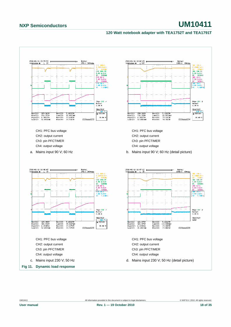
3.4.4 Dynamic load responseTest conditions:
• The adapter is subjected to a load change from 0 % to 100 % at a slew rate of 1 A/ms• The frequency of change is set to provide the best readability of the deviation and
setting time
Remark: The voltage is measured at the end of the output cable.
Pass criteria:
The output must not overshoot or undershoot beyond the specified limits (+1 V to 0.5 V) after a load change.
Table 11. Ripple and noise PARD Ripple and noise (at maximum load) as a function of the mains input voltage.
Mains supply 90 V; 60 Hz 100 V; 50 Hz 115 V; 60 Hz 230 V; 50 Hz 264 V; 50 HzPARD (mV) 86 86 86 75 75
Table 12. Dynamic load response Deviation of the output voltage at a load step from 6.15 A to 0 A and from 0 A to 6.15 A
Mains supply 90 V; 60 Hz 100 V; 50 Hz 115 V; 60 Hz 230 V; 50 Hz 264 V; 50 HzDeviation (mVp-p) 700 700 700 700 700
UM10411 All information provided in this document is subject to legal disclaimers. © NXP B.V. 2010. All rights reserved.
User manual Rev. 1 — 19 October 2010 17 of 35
NXP Semiconductors UM10411120 Watt notebook adapter with TEA1752T and TEA1791T
CH1: PFC bus voltageCH2: output currentCh3: pin PFCTIMERCh4: output voltage
CH1: PFC bus voltageCH2: output currentCh3: pin PFCTIMERCh4: output voltage
a. Mains input 90 V; 60 Hz b. Mains input 90 V; 60 Hz (detail picture)
CH1: PFC bus voltageCH2: output currentCh3: pin PFCTIMERCh4: output voltage
CH1: PFC bus voltageCH2: output currentCh3: pin PFCTIMERCh4: output voltage
c. Mains input 230 V; 50 Hz d. Mains input 230 V; 50 Hz (detail picture)
Fig 11. Dynamic load response
019aaa023 019aaa024
019aaa025 019aaa026
UM10411 All information provided in this document is subject to legal disclaimers. © NXP B.V. 2010. All rights reserved.
User manual Rev. 1 — 19 October 2010 18 of 35
NXP Semiconductors UM10411120 Watt notebook adapter with TEA1752T and TEA1791T
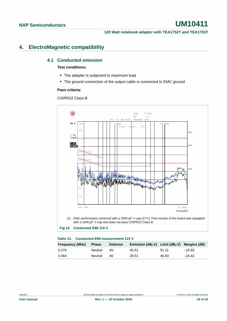
4. ElectroMagnetic compatibility
4.1 Conducted emissionTest conditions:
• The adapter is subjected to maximum load• The ground connection of the output cable is connected to EMC ground
Pass criteria:
CISPR22 Class B
(1) EMC performance achieved with a 3300 pF Y-cap (CY1). First version of the board was equipped with a 1000 pF Y-cap and does not pass CISPR22 Class B.
Fig 12. Conducted EMI 115 V
Table 13. Conducted EMI measurement 115 V Frequency (MHz) Phase Detector Emission (dBμV) Limit (dBμV) Margins (dB)0.270 Neutral AV 40.51 51.11 −10.60
0.464 Neutral AV 28.51 46.93 −18.42
150 kHz 30 MHz
1 PKCLRWR
2 AVCLRWR
SGL
TDF
6DB
dB�VdB�V
RBW 9 kHzMT 1 sPREAMP OFFAtt 10 dB AUTO
1 MHz 10 MHz
0
10
20
30
40
50
60
70
80
90
100LIMIT CHECK PASS
EN55022A
EN55022Q
019aaa880
UM10411 All information provided in this document is subject to legal disclaimers. © NXP B.V. 2010. All rights reserved.
User manual Rev. 1 — 19 October 2010 19 of 35

NXP Semiconductors UM10411120 Watt notebook adapter with TEA1752T and TEA1791T
(1) EMC performance achieved with a 3300 pF Y-cap (CY1). First version of the board was equipped with a 1000 pF Y-cap and does not pass CISPR22 class B.
Fig 13. Conducted EMI 230 V
Table 14. Conducted EMI measurement 230 V Frequency (MHz) Phase Detector Emission (dBμV) Limit (dBμV) Margins (dB)0.198 Line AV 51.59 53.69 −2.10
0.202 Neutral QP 50.25 63.52 −13.27
0.262 Line AV 41.29 51.36 −10.07
0.374 Neutral QP 48.19 58.40 −10.21
0.374 Neutral AV 35.77 48.41 −12.64
0.398 Neutral AV 36.59 47.89 −11.30
0.462 Neutral AV 39.25 46.65 −7.40
0.526 Neutral AV 37.59 46.00 −8.40
0.570 Line AV 28.46 46.00 −17.53
0.742 Line QP 47.43 46.00 −8.56
0.742 Line AV 30.71 46.00 −15.28
0.766 Line QP 45.60 46.00 −10.39
0.766 Line AV 29.19 46.00 −16.80
0.854 Neutral AV 35.46 46.00 −10.53
1.114 Neutral AV 33.06 46.00 −12.93
1.186 Neutral AV 34.50 46.00 −11.49
150 kHz 30 MHz
1 PKCLRWR
2 AVCLRWR
SGL
TDF
6DB
dB�VdB�V
RBW 9 kHzMT 1 sPREAMP OFFAtt 10 dB AUTO
1 MHz 10 MHz
0
10
20
30
40
50
60
70
80
90
100LIMIT CHECK PASS
EN55022A
EN55022Q
019aaa881
UM10411 All information provided in this document is subject to legal disclaimers. © NXP B.V. 2010. All rights reserved.
User manual Rev. 1 — 19 October 2010 20 of 35

NXP Semiconductors UM10411120 Watt notebook adapter with TEA1752T and TEA1791T
4.2 Immunity against lighting surgesTest conditions:
• Combination wave: 1.2/50 μs open circuit voltage and 8/20 μs short-circuit current• Test voltage: 2 kV• L1 to L2: 2 Ω; L1 to PE, L2 to PE and L1 + L2 to PE: 12 Ω• Phase angle: 0 °, 90 °, 180 ° and 270 °• Number of tests: 5 positive and 5 negative• Pulse repetition rate: 20 s
Test result:
• There is no disruption of functionality
4.3 Immunity against ESDTest conditions:
• ESD air discharge at the ground contact of the output cable
Pass criteria:
• IEC61000-4-2 air discharge level 3 (8 kV) and level 4 (15 kV)
Table 15. Immunity against ESD Performance of the adapter at an ESD air discharge
ESD performance No disruption of function
Auto recovery
Demo board according to schematic ±12 kV ±15 kV
Demo board with 6 M x 10 M across Y-cap ±16.5 kV -
UM10411 All information provided in this document is subject to legal disclaimers. © NXP B.V. 2010. All rights reserved.
User manual Rev. 1 — 19 October 2010 21 of 35

NXP Semiconductors UM10411120 Watt notebook adapter with TEA1752T and TEA1791T
4.4 Mains harmonic reduction (MHR)Test conditions:
• The adapter is set to the maximum continuous load of 6.15 A• The input voltage is 230 V; 50 Hz
Pass criteria:
• Compliance with EN61000-3-2 A14 class D
Test result:
• Passed, see Table 16
Table 16. MHR according EN61000-3-2 A14, class D Harmonic number
Measured (mA) Limit (mA) Harmonic number
Measured (mA) Limit (mA)
1 588.3 - 21 2.2 26.6
3 110.3 446.9 23 2.6 24.1
5 54.6 249.8 25 7.8 22.0
7 17.5 131.5 27 5.5 20.2
9 10.5 65.7 29 3.7 18.7
11 6.2 46.0 31 5.6 17.5
13 15.0 46.0 33 2.7 16.3
15 8.1 38.9 35 1.5 15.3
17 6.9 33.7 37 3.4 14.5
19 4.4 29.8 39 5.0 13.7
UM10411 All information provided in this document is subject to legal disclaimers. © NXP B.V. 2010. All rights reserved.
User manual Rev. 1 — 19 October 2010 22 of 35
xxxx xxxxxxxxxxxxxxxxxxxxxxxxxxxxxx x xxxxxxxxxxxxxx xxxxxxxxxx xxx xxxxxx xxxxxxxxxxxxxxxxxxxxxxx xxxxxxxxxxxxxxxxxxxxxx xxxxx xxxxxx xx xxxxxxxxxxxxxxxxxxxxxxxxxxxxx xxxxxxxxxxxxxxxxxxxxxx xxxxxxxxxxx xxxxxxx xxxxxxxxxxxxxxxxxxx xxxxxxxxxxxxxxxx xxxxxxxxxxxxxx xxxxxx xx xxxxxxxxxxxxxxxxxxxxxxxxxxxxxxxx xxxxxxxxxxxxxxxxxxxxxxxx xxxxxxx xxxxxxxxxxxxxxxxxxxxxxxxxxxxxxxxxxxxxxxxxxxxxx xxxxxxxxxxx xxxxx x x
UM
10411
User m
anual
NXP Sem
iconducto
5. Schem
atic
BC1D1L2L1
rsUM10411
120 Watt notebook adapter w
ith TEA1752T and TEA
1791T
019aaa050
R32
C27 C28 C29
C18
R25
C31 L3
8
7
3567
SR
SE
NS
E
Vo +
Vo −
n.c.n.c.n.c.n.c.1
3
791T
All information provided in this docum
ent is subject to legal disclaimers.
© N
XP B.V. 2010. All rights reserved.
Rev. 1 —
19 October 2010
23 of 35
Fig 14. Schematic of 120 W TEA1752T and TEA1791T adapter solution
C19C21
C2
C22
C18
C14
C4
C9
C8
C30
R30
Q4
D3
R18
C23
C13
C3AC3
C15
U2
C17
C20 R26
R15A R15
R10
RT2NTC
R4
R7
R5A
R6A
R5
R23A D23A
R25
R20
C12
R33
R35
C35 R36
R6
C34
C10
C6
U4
R34
R3
R3
C16
R24
R3
CY1 BC2
R27
R23
R16
R22
R17
R16A
R1
F1 RT1NTC
CX1
R2
R14 R13
D4
T1D30
C1BD1
+
−
R9 R8
R12 R11
D2
LF2
Q2
C5Q1
D5
14 7
11PFCSENSE
PFCTIMER
12PFCDRIVER
8PFCAUX
FBAUX4
FBCTRL3
4
3
5
1
4
2 11
7, 8
9, 10
8
2
DR
IVE
R
4
VCC
GND
9
12
7
1
6
1
2
PFCCOMP6
15
HV
S
9V
OS
EN
SE
13F
BD
RIV
ER
10
FB
SE
NS
E
16
HV
1
VC
C
VIN
SE
NS
E
2
GN
D
5LA
TC
H
U1
TEA1752T
U
TEA1
LF1
MAINS INLET
C24
Q3C25
R28
D6
Θ
Θ
NXP Semiconductors UM10411120 Watt notebook adapter with TEA1752T and TEA1791T
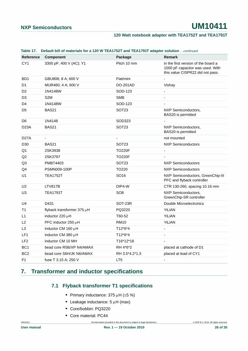
6. Bill of materials
Table 17. Default bill of materials for a 120 W TEA1752T and TEA1791T adapter solution Reference Component Package RemarkR1 2 MΩ, 1 % 1206 -
R2 2 MΩ, 1 % 1206 -
R3 560 kΩ, 1 % 1206 -
R4 47 kΩ, 1 % 0603 -
R5 2 MΩ, 1 % 1206 -
R5A 1.3 MΩ, 1 % 1206 -
R6 2.7 MΩ, 1 % 1206 -
R6A 2.7 MΩ, 1 % 1206 -
R7 60.4 kΩ, 1 % 0603 -
R8 10 Ω, 5 % 0805 -
R9 10 Ω, 5 % 0805 -
R10 0.1 Ω, 5 %; 1 W axial metal-oxide film
R11 15 kΩ, 5 % 0603 -
R12 1 kΩ, 5 % 0805 -
R13 10 Ω, 5 % 0805 -
R14 10 Ω, 5 % 0805 -
R15 0.1 Ω, 5 %; 1 W axial metal-oxide film
R15A - - not mounted
R16 39 kΩ, 5 % 0603 -
R16A 1.2 kΩ, 5 % 0603 -
R17 820 Ω, 5 % 0603 -
R18 43 kΩ, 5 % 1206 -
R19 43 kΩ, 5 % 1206 -
R20 47 Ω, 5 % 0805 -
R21 0 Ω 0805 -
R22 10 kΩ, 5 % 0805 -
R23 82 kΩ, 1 % 0603 -
R23A 330 kΩ, 1 % 0603 -
R24 39 kΩ, 5 % 0603 -
R25 39 kΩ, 5 % 0603 -
R26 10 kΩ, 5 % 0603 -
R27 5.1 kΩ, 5 % 1206 -
R28 0 Ω 0603 -
R29 - - not mounted
R30 10 Ω, 5 % 0805 -
R32 1 kΩ, 5 % 0805 -
R33 - - not mounted
R34 1 kΩ, 5 % 0603 -
UM10411 All information provided in this document is subject to legal disclaimers. © NXP B.V. 2010. All rights reserved.
User manual Rev. 1 — 19 October 2010 24 of 35

NXP Semiconductors UM10411120 Watt notebook adapter with TEA1752T and TEA1791T
R35 3 kΩ, 5 % 0603 -
R36 10 kΩ, 5 % 0603 -
R37 35.7 kΩ, 1 % 0603 -
R38 5.23 kΩ, 1 % 0603 -
R39 - - not mounted
RT1 jumper - -
RT2 NTC 100 kΩ; D = 5 mm radial lead TTC050104
C1 film capacitor 0.47 μF; 450 V, 10 % - -
C2 film capacitor 0.47 μF; 450V, 10 % - -
C3 electrolytic capacitor 120 μF; 400V; 105 °C
radial 18 × 32 mm -
C3A 10 nF; 1 kV; Z5U Disk 11.5 mm -
C4 10 nF; 25 V; X7R 0603 -
C5 220 pF; 630 V; NP0 1206 -
C6 0.1 μF; 25 V; X7R 0603 -
C8 3300 pF; 630 V 1206 -
C9 100 pF; 630 V; NP0 1206 -
C10 0.1 μF; 25 V; X7R 0805 -
C12 220 pF; 100 V; NP0 0805 -
C13 electrolytic capacitor 47 μF; 35V; 105 °C radial 5 × 11 mm low-impedance type
C14 1 μF; 50 V; Y5V 0805 -
C15 10 nF; 25 V; X7R 0603 -
C16 0.33 μF; 10 V; X7R 0603 timing capacitor; review tolerance
C17 0.33 μF; 10 V; X7R 0603 -
C18 0.47 μF; 10 V; X7R 0603 -
C19 10 nF; 25 V; X7R 0603 -
C20 2.2 μF; 10 V; Y5V 0603 -
C21 2.2 μF; 10 V; Y5V 0603 -
C22 220 pF; 50 V; NP0 0603 10 V is permitted
C23 220 pF; 50 V; NP0 0603 10 V is permitted
C24 1 nF; 50 V; X7R 0603 10 V is permitted
C25 1 μF; 16 V; X7R 0603 10 V is permitted
C27 electrolytic capacitor 680 μF; 25V; 105 °C Radial 10 × 16 mm low-impedance type
C28 electrolytic capacitor 680 μF; 25V; 105 °C Radial 10 × 16 mm low-impedance type
C29 electrolytic capacitor 680 μF; 25V; 105 °C Radial 10 × 16 mm low-impedance type
C30 1 μF; 50 V; Y5V 0805 -
C31 - - not mounted
C34 0.1 μF; 25 V; X7R 0603 -
C35 10 nF; 25 V; X7R 0603 -
C36 - - not mounted
CX1 0.47 μF; 275 V (AC); X2 MKP -
Table 17. Default bill of materials for a 120 W TEA1752T and TEA1791T adapter solution …continued
Reference Component Package Remark
UM10411 All information provided in this document is subject to legal disclaimers. © NXP B.V. 2010. All rights reserved.
User manual Rev. 1 — 19 October 2010 25 of 35
NXP Semiconductors UM10411120 Watt notebook adapter with TEA1752T and TEA1791T
7. Transformer and inductor specifications
7.1 Flyback transformer T1 specifications
• Primary inductance: 375 μH (±5 %)• Leakage inductance: 5 μH (max)• Core/bobbin: PQ3220• Core material: PC44
CY1 3300 pF; 400 V (AC); Y1 Pitch 10 mm in the first version of the board a 1000 pF capacitor was used. With this value CISPR22 did not pass.
BD1 GBU806; 8 A; 600 V Flat/mini -
D1 MUR460; 4 A; 600 V DO-201AD Vishay
D2 1N4148W SOD-123 -
D3 S2M SMB -
D4 1N4148W SOD-123 -
D5 BAS21 SOT23 NXP Semiconductors, BAS20 is permitted
D6 1N4148 SOD323 -
D23A BAS21 SOT23 NXP Semiconductors, BAS20 is permitted
D27A - - not mounted
D30 BAS21 SOT23 NXP Semiconductors
Q1 2SK3938 TO220F -
Q2 2SK3797 TO220F -
Q3 PMBT4403 SOT23 NXP Semiconductors
Q4 PSMN009-100P TO220 NXP Semiconductors
U1 TEA1752T SO16 NXP Semiconductors, GreenChip-III PFC and flyback controller
U2 LTV817B DIP4-W CTR 130-260, spacing 10.16 mm
U3 TEA1791T SO8 NXP Semiconductors, GreenChip-SR controller
U4 D431 SOT-23R Double Microelectronics
T1 flyback transformer 375 μH PQ3220 YiLiAN
L1 inductor 220 μH T60-52 YiLiAN
L2 PFC inductor 250 μH RM10 YiLiAN
L3 inductor CM 160 μH T12*6*4 -
LF1 inductor CM 380 μH T12*6*4 -
LF2 inductor CM 10 MH T16*12*18 -
BC1 bead core R5B/XP N4/AMAX RH 4*6*2 placed at cathode of D1
BC2 bead core S6H/JK N6/AMAX RH 3.5*4.2*1.3 placed at lead of CY1
F1 fuse T 3.15 A; 250 V LT5 -
Table 17. Default bill of materials for a 120 W TEA1752T and TEA1791T adapter solution …continued
Reference Component Package Remark
UM10411 All information provided in this document is subject to legal disclaimers. © NXP B.V. 2010. All rights reserved.
User manual Rev. 1 — 19 October 2010 26 of 35

NXP Semiconductors UM10411120 Watt notebook adapter with TEA1752T and TEA1791T
• Hi-POT primary and secondary: 3 kV; 5 mA; 3 s
Manufacturer: YiLiAN, LTD, Taiwan ROC.
Fig 15. Flyback transformer schematic
Teflon tube
Start
E1, E2, E3, E4
N1, N67
9
10
8
11
2
4
1
5
6
N4, N7
N8
N5
N2
N3
Black teflon tube
Primary Secondary
Bobbin
N1
Tape
N2
N3
N4
E2
N5
N6
N7
N8
E1
E4
E3
014aab118
Table 18. Flyback transformer winding details Winding order
Pin number Wire type Number of wires
Number of turns RemarksStart Finish Winding MYLAR tape
1 N1 7 9 TIW. 0.3 mm diameter 2 6 1 TEX-E
2 E1 - 6 copper foil 0.025 mm × 7 mm
- 1 1 finished with wire 0.3 mm diameter
3 N2 1 4 2UEW 0.5 mm diameter 1 16 1 -
4 E2 - 6 copper foil 0.025 mm × 7 mm
- 1 1 finished with wire 0.3 mm diameter
5 N3 5 6 2UEW 0.25 mm diameter 2 7 1 -
6 N4 8 10 TIW. 0.3 mm diameter 2 6 1 TEX-E
7 E3 - 6 copper foil 0.025 mm × 7 mm
- 1 1 finished with wire 0.3 mm diameter
8 N5 4 2 2UEW 0.5 mm 1 16 1 -
9 E4 - 6 copper foil 0.025 mm × 7 mm
- 1 1 finished with wire 0.3 mm diameter
10 N6 7 9 TIW. 0.3 mm diameter 2 6 1 TEX-E
11 N7 8 10 TIW. 0.3 mm diameter 2 6 1 TEX-E
12 N8 11 8 TIW. 0.3 mm diameter 1 5 3 TEX-E; close winding method
UM10411 All information provided in this document is subject to legal disclaimers. © NXP B.V. 2010. All rights reserved.
User manual Rev. 1 — 19 October 2010 27 of 35

NXP Semiconductors UM10411120 Watt notebook adapter with TEA1752T and TEA1791T
7.2 PFC inductor L2 specifications
• Primary inductance: 250 μH (±10 %)• Core/bobbin: RM10• Core material: NC-2H
Manufacturer: YiLiAN, LTD, Taiwan ROC.
Fig 16. PFC inductor L2 schematic
Teflon tube
Start
E1, E2
N212
1
9
7N1
Primary Auxilary
Bobbin
N1
Tape
N2
014aab121
Table 19. PFC inductor L2 winding details Winding order
Pin no. Winding type Number of wires
Number turns RemarksStart Finish Winding MYLAR tape
1 N1 9 7 USTC 0.1 mm diameter
30 40 turns 1 turn -
2 N2 12 1 2UEW 0.22 mm diameter
2 2.5 turns 3 turns -
UM10411 All information provided in this document is subject to legal disclaimers. © NXP B.V. 2010. All rights reserved.
User manual Rev. 1 — 19 October 2010 28 of 35

NXP Semiconductors UM10411120 Watt notebook adapter with TEA1752T and TEA1791T
8. PCB layout
The SMPS printed-circuit board is a single-sided board. Dimensions are 125 mm x 59 mm.
The PCBs are 1.6 mm FR2 with single-sided 2 oz. copper (70 m) layer.
The Gerber file set for production of the PCB is available through the local NXP Semiconductors sales office
Fig 17. Demo board top silk (top view)
001aak822
R10
D1Q1
C2C1
CX1
B01
LF2
CN1 F1
FG
RT1HS2
LF1
L2
APBADC031 Ver. A
−U +U
T3.
15 A
/250
V
C3L1
C3A
J3
BC1
R15
J1
C13 RT2
T1 U2Q4
C27
C28
C29
J2
L3BC2CY1Q2
HS1
Fig 18. Demo board bottom silk (bottom view)
001aak823
R13
C8
D3
C9
R21
C12
D5
R29
R6AR6
R16AR16C10
D6C25R28C24 R14
C14
C15
C19C17 C18
C21C20
C16
R26R24
R23
D30
C30
U3
Q3
D4
R33
C31 R32 R30
R18
R19
R37
R36
C35
R39
C36
C34
R38
U4
R35
R34
D23A
R23A
R20
R15BR15A
R5
R5AR8D2
R1
R2
90W
120W
TEA1751
TEA1752
R27
R3R4
D27A
C22R12R7
R9
C23
R25
U1
R22
C6R11
R17C4
C5
UM10411 All information provided in this document is subject to legal disclaimers. © NXP B.V. 2010. All rights reserved.
User manual Rev. 1 — 19 October 2010 29 of 35

NXP Semiconductors UM10411120 Watt notebook adapter with TEA1752T and TEA1791T
Fig 19. Demo board bottom copper (bottom view)
001aak824
UM10411 All information provided in this document is subject to legal disclaimers. © NXP B.V. 2010. All rights reserved.
User manual Rev. 1 — 19 October 2010 30 of 35

NXP Semiconductors UM10411120 Watt notebook adapter with TEA1752T and TEA1791T
9. Abbreviations
Table 20. Abbreviations tableAcronym DescriptionCC Constant Current
EMC ElectroMagnetic Compatibility
EMI ElectroMagnetic Interference
ESD ElectroStatic Discharge
FLR Fast Latch Reset
LISN Line Impedance Standardization Network
MHR Mains Harmonic Reduction
OTP OverTemperature Protection
OCP OverCurrent Protection
OVP OverVoltage Protection
PE Protective Earth
PFC Power Factor Correction
SCP Short-Circuit Protection
SMPS Switched Mode Power Supply
SR Synchronous Rectification
TIW Triple Insulated Wire
UEW polyUrethane Enameled Wire
USTC polyUrethane Silk Tetrone Covered
UM10411 All information provided in this document is subject to legal disclaimers. © NXP B.V. 2010. All rights reserved.
User manual Rev. 1 — 19 October 2010 31 of 35

NXP Semiconductors UM10411120 Watt notebook adapter with TEA1752T and TEA1791T
10. Legal information
10.1 DefinitionsDraft — The document is a draft version only. The content is still under internal review and subject to formal approval, which may result in modifications or additions. NXP Semiconductors does not give any representations or warranties as to the accuracy or completeness of information included herein and shall have no liability for the consequences of use of such information.
10.2 DisclaimersLimited warranty and liability — Information in this document is believed to be accurate and reliable. However, NXP Semiconductors does not give any representations or warranties, expressed or implied, as to the accuracy or completeness of such information and shall have no liability for the consequences of use of such information.
In no event shall NXP Semiconductors be liable for any indirect, incidental, punitive, special or consequential damages (including - without limitation - lost profits, lost savings, business interruption, costs related to the removal or replacement of any products or rework charges) whether or not such damages are based on tort (including negligence), warranty, breach of contract or any other legal theory.
Notwithstanding any damages that customer might incur for any reason whatsoever, NXP Semiconductors’ aggregate and cumulative liability towards customer for the products described herein shall be limited in accordance with the Terms and conditions of commercial sale of NXP Semiconductors.
Right to make changes — NXP Semiconductors reserves the right to make changes to information published in this document, including without limitation specifications and product descriptions, at any time and without notice. This document supersedes and replaces all information supplied prior to the publication hereof.
Suitability for use — NXP Semiconductors products are not designed, authorized or warranted to be suitable for use in life support, life-critical or safety-critical systems or equipment, nor in applications where failure or malfunction of an NXP Semiconductors product can reasonably be expected to result in personal injury, death or severe property or environmental damage. NXP Semiconductors accepts no liability for inclusion and/or use of NXP Semiconductors products in such equipment or applications and therefore such inclusion and/or use is at the customer’s own risk.
Applications — Applications that are described herein for any of these products are for illustrative purposes only. NXP Semiconductors makes no representation or warranty that such applications will be suitable for the specified use without further testing or modification.
Customers are responsible for the design and operation of their applications and products using NXP Semiconductors products, and NXP Semiconductors accepts no liability for any assistance with applications or customer product design. It is customer’s sole responsibility to determine whether the NXP Semiconductors product is suitable and fit for the customer’s applications and products planned, as well as for the planned application and use of customer’s third party customer(s). Customers should provide appropriate design and operating safeguards to minimize the risks associated with their applications and products.
NXP Semiconductors does not accept any liability related to any default, damage, costs or problem which is based on any weakness or default in the customer’s applications or products, or the application or use by customer’s third party customer(s). Customer is responsible for doing all necessary testing for the customer’s applications and products using NXP Semiconductors products in order to avoid a default of the applications and the products or of the application or use by customer’s third party customer(s). NXP does not accept any liability in this respect.
Export control — This document as well as the item(s) described herein may be subject to export control regulations. Export might require a prior authorization from national authorities.
Evaluation products — This product is provided on an “as is” and “with all faults” basis for evaluation purposes only. NXP Semiconductors, its affiliates and their suppliers expressly disclaim all warranties, whether express, implied or statutory, including but not limited to the implied warranties of non-infringement, merchantability and fitness for a particular purpose. The entire risk as to the quality, or arising out of the use or performance, of this product remains with customer.
In no event shall NXP Semiconductors, its affiliates or their suppliers be liable to customer for any special, indirect, consequential, punitive or incidental damages (including without limitation damages for loss of business, business interruption, loss of use, loss of data or information, and the like) arising out the use of or inability to use the product, whether or not based on tort (including negligence), strict liability, breach of contract, breach of warranty or any other theory, even if advised of the possibility of such damages.
Notwithstanding any damages that customer might incur for any reason whatsoever (including without limitation, all damages referenced above and all direct or general damages), the entire liability of NXP Semiconductors, its affiliates and their suppliers and customer’s exclusive remedy for all of the foregoing shall be limited to actual damages incurred by customer based on reasonable reliance up to the greater of the amount actually paid by customer for the product or five dollars (US$5.00). The foregoing limitations, exclusions and disclaimers shall apply to the maximum extent permitted by applicable law, even if any remedy fails of its essential purpose.
Safety of high-voltage evaluation products — The non-insulated high voltages that are present when operating this product, constitute a risk of electric shock, personal injury, death and/or ignition of fire. This product is intended for evaluation purposes only. It shall be operated in a designated test area by personnel that is qualified according to local requirements and labor laws to work with non-insulated mains voltages and high-voltage circuits.
The product does not comply with IEC 60950 based national or regional safety standards. NXP Semiconductors does not accept any liability for damages incurred due to inappropriate use of this product or related to non-insulated high voltages. Any use of this product is at customer’s own risk and liability. The customer shall fully indemnify and hold harmless NXP Semiconductors from any liability, damages and claims resulting from the use of the product.
10.3 TrademarksNotice: All referenced brands, product names, service names and trademarks are the property of their respective owners.
GreenChip — is a trademark of NXP B.V.
UM10411 All information provided in this document is subject to legal disclaimers. © NXP B.V. 2010. All rights reserved.
User manual Rev. 1 — 19 October 2010 32 of 35

NXP Semiconductors UM10411120 Watt notebook adapter with TEA1752T and TEA1791T
11. Tables
Table 1. Active mode efficiency at 115 V; 60 Hz . . . . . . .6Table 2. Active mode efficiency at 230 V; 50 Hz . . . . . .6Table 3. PFC on and off level as a function of mains
input voltage . . . . . . . . . . . . . . . . . . . . . . . . . . .6Table 4. No-load input power . . . . . . . . . . . . . . . . . . . . .7Table 5. PFC plus flyback stage . . . . . . . . . . . . . . . . . . .7Table 6. Output short-circuit input power . . . . . . . . . . . .12Table 7. Output OCP and input power as a function
of the mains input voltage . . . . . . . . . . . . . . . .12Table 8. Output OVP . . . . . . . . . . . . . . . . . . . . . . . . . .12Table 9. Load regulation . . . . . . . . . . . . . . . . . . . . . . . .15Table 10. Line regulation . . . . . . . . . . . . . . . . . . . . . . . .16Table 11. Ripple and noise PARD . . . . . . . . . . . . . . . . .17Table 12. Dynamic load response . . . . . . . . . . . . . . . . .17Table 13. Conducted EMI measurement 115 V . . . . . . . .19Table 14. Conducted EMI measurement 230 V . . . . . . .20Table 15. Immunity against ESD . . . . . . . . . . . . . . . . . .21Table 16. MHR according EN61000-3-2 A14, class D . .22Table 17. Default bill of materials for a 120 W TEA1752T
and TEA1791T adapter solution . . . . . . . . . . .24Table 18. Flyback transformer winding details . . . . . . . .27Table 19. PFC inductor L2 winding details . . . . . . . . . . .28Table 20. Abbreviations table . . . . . . . . . . . . . . . . . . . . . .31
UM10411 All information provided in this document is subject to legal disclaimers. © NXP B.V. 2010. All rights reserved.
User manual Rev. 1 — 19 October 2010 33 of 35
continued >>

NXP Semiconductors UM10411120 Watt notebook adapter with TEA1752T and TEA1791T
12. Figures
Fig 1. 120 W TEA1752T and TEA1791T demo board . . .4Fig 2. Delay between switch-on and output in
regulation . . . . . . . . . . . . . . . . . . . . . . . . . . . . . . . .8Fig 3. Output rise time at full load start-up . . . . . . . . . . . .8Fig 4. Brownout and brownout recovery . . . . . . . . . . . . .9Fig 5. Output short-circuit, triggering of the time-out
protection . . . . . . . . . . . . . . . . . . . . . . . . . . . . . . .10Fig 6. Output short-circuit at 90 V; 60 Hz. . . . . . . . . . . . 11Fig 7. Output short-circuit at 264 V; 50 Hz. . . . . . . . . . . 11Fig 8. Output OVP . . . . . . . . . . . . . . . . . . . . . . . . . . . . .13Fig 9. External OTP . . . . . . . . . . . . . . . . . . . . . . . . . . . .14Fig 10. Fast latch reset . . . . . . . . . . . . . . . . . . . . . . . . . .15Fig 11. Dynamic load response . . . . . . . . . . . . . . . . . . . .18Fig 12. Conducted EMI 115 V . . . . . . . . . . . . . . . . . . . . .19Fig 13. Conducted EMI 230 V . . . . . . . . . . . . . . . . . . . . .20Fig 14. Schematic of 120 W TEA1752T and
TEA1791T adapter solution . . . . . . . . . . . . . . . . .23Fig 15. Flyback transformer schematic . . . . . . . . . . . . . .27Fig 16. PFC inductor L2 schematic . . . . . . . . . . . . . . . . .28Fig 17. Demo board top silk (top view) . . . . . . . . . . . . . .29Fig 18. Demo board bottom silk (bottom view) . . . . . . . .29Fig 19. Demo board bottom copper (bottom view). . . . . .30
UM10411 All information provided in this document is subject to legal disclaimers. © NXP B.V. 2010. All rights reserved.
User manual Rev. 1 — 19 October 2010 34 of 35
continued >>
NXP Semiconductors UM10411120 Watt notebook adapter with TEA1752T and TEA1791T
13. Contents
1 Introduction . . . . . . . . . . . . . . . . . . . . . . . . . . . . 32 Specification. . . . . . . . . . . . . . . . . . . . . . . . . . . . 43 Performance data. . . . . . . . . . . . . . . . . . . . . . . . 53.1 Test setup . . . . . . . . . . . . . . . . . . . . . . . . . . . . . 53.1.1 Test equipment . . . . . . . . . . . . . . . . . . . . . . . . . 53.1.2 Test conditions . . . . . . . . . . . . . . . . . . . . . . . . . 53.2 Efficiency . . . . . . . . . . . . . . . . . . . . . . . . . . . . . 53.2.1 ENERGY STAR efficiency . . . . . . . . . . . . . . . . 53.2.1.1 Active mode efficiency . . . . . . . . . . . . . . . . . . . 53.2.1.2 No-load input power . . . . . . . . . . . . . . . . . . . . . 63.2.1.3 Full load efficiency PFC plus flyback stage . . . 73.3 Timing and protection . . . . . . . . . . . . . . . . . . . . 73.3.1 Switch-on delay and output rise time . . . . . . . . 73.3.2 Brownout and brownout recovery. . . . . . . . . . . 93.3.3 Output short-circuit protection . . . . . . . . . . . . . 93.3.4 Output OverCurrent protection . . . . . . . . . . . . 123.3.5 Output OverVoltage protection . . . . . . . . . . . . 123.3.6 OverTemperature protection. . . . . . . . . . . . . . 133.3.7 Fast latch reset . . . . . . . . . . . . . . . . . . . . . . . . 143.4 Output regulation and characterization. . . . . . 153.4.1 Load regulation. . . . . . . . . . . . . . . . . . . . . . . . 153.4.2 Line regulation . . . . . . . . . . . . . . . . . . . . . . . . 163.4.3 Ripple and noise periodic and random
deviation . . . . . . . . . . . . . . . . . . . . . . . . . . . . . 163.4.4 Dynamic load response . . . . . . . . . . . . . . . . . 174 ElectroMagnetic compatibility . . . . . . . . . . . . 194.1 Conducted emission . . . . . . . . . . . . . . . . . . . . 194.2 Immunity against lighting surges . . . . . . . . . . 214.3 Immunity against ESD . . . . . . . . . . . . . . . . . . 214.4 Mains harmonic reduction (MHR). . . . . . . . . . 225 Schematic. . . . . . . . . . . . . . . . . . . . . . . . . . . . . 236 Bill of materials . . . . . . . . . . . . . . . . . . . . . . . . 247 Transformer and inductor specifications . . . 267.1 Flyback transformer T1 specifications . . . . . . 267.2 PFC inductor L2 specifications . . . . . . . . . . . . 288 PCB layout . . . . . . . . . . . . . . . . . . . . . . . . . . . . 299 Abbreviations. . . . . . . . . . . . . . . . . . . . . . . . . . 3110 Legal information. . . . . . . . . . . . . . . . . . . . . . . 3210.1 Definitions. . . . . . . . . . . . . . . . . . . . . . . . . . . . 3210.2 Disclaimers . . . . . . . . . . . . . . . . . . . . . . . . . . . 3210.3 Trademarks. . . . . . . . . . . . . . . . . . . . . . . . . . . 3211 Tables . . . . . . . . . . . . . . . . . . . . . . . . . . . . . . . . 3312 Figures . . . . . . . . . . . . . . . . . . . . . . . . . . . . . . . 3413 Contents . . . . . . . . . . . . . . . . . . . . . . . . . . . . . . 35
© NXP B.V. 2010. All rights reserved.For more information, please visit: http://www.nxp.com For sales office addresses, please send an email to: [email protected]
Date of release: 19 October 2010Document identifier: UM10411
Please be aware that important notices concerning this document and the product(s) described herein, have been included in section ‘Legal information’.