unclassified ad 405 778k - defense technical … · figures 1. assumed diode ... capacitive...
TRANSCRIPT

UNCLASSIFIED
AD 405 778k
DEFENSE DOCUMENTATION CENTERFOB
SC.[l' F A,,D TECHNICAL INFORMATION
CAME'RON 'MTATION, ALEXANDRIA, VIRGINIA
UNCLASSIFIED

NOTICE: When government or other drawings, speci-fications or other data are used for any purposeother than in connection with a definitely relatedgovernment procurement operation, the U. S.Government thereby incurs no responsibility, nor anyobligation whatsoever; and the fact that the Govern-ment may have formulated, furnished, or in any waysupplied the said drawings, specifications, or otherdata is not to be regarded by implication or other-wise as in any manner licensing the holder or o--other person or corporation, or conveying any rightsor permission to manufacture, use or sell anypatented invention that may in any way be relatedthereto.

405 778 "00 8j USAELMDL Tecbnical -Report 2349
X-BAIMD SEMaCOXDUCOR SWITCHEWJ AND LMITInG USIING WAVEUIDE'SM1RI TEW
'- ri 51-2ir J
March 1963 DDC
JUN 6 1963
TISIA B
UNITED STATES ARMY
ELECTRONICS RESEARCH, AND DEVELOPMENT LABORATORY
FORT MONMOUTH, N.J.

U. S. ARM ELECTRONICS RESEARCH AND DEVELOP1NT IABORATOCYFORT MOKOtuH, NEL JERSEY
March 1963
3SAETLDL Technical Report 2349 has been prepared under the supervisionof the Director, Electronic Components Department, and is published for theinformation and guidance of all concerned. Suggestions or criticismsrelative to the form, contents, purpose, or use of this publication shouldbe referred to the Comanding Officer, U. S. Army Electronics Research andDevelopment Laboratory, Fort Monmouth, New Jersey, Attn: Chief, Microwaveand Quantum Electronics Branch, Solid State and Frequency Control Division.
J. M. KILM=OUGH, JR.Colonel, Signal CorpsCommnding
OKJTCIAL:HOWARD W. KILLAMMajor, SigCAdjutant
DISTRIBUTION:Special
QUALIFIED REQUESTERS MAY OBTAINCOPIES OF THIS REPORT FROM ASTIA.
THIS REPORT HAS BEEN RELEASED TO THOFFICE OF TECHNICAL SERVICES, U. S. DEPAB TOF COMWHTCE, WAS=NGTON 25, D. C., FOR SALE TOTH GE=IAL PUBLIC.

X-BA1D SEMICOINUCTOR SWITCH11NG AND LIMTING USIN WAVEGJIDE SERIES TEES
V. J. Higgins
DA Task Nr. ;A99-21-0O1-03
Abstract
This report describes a new microwve semiconductor switching techniqueX-band. This technique uses various types of varactor diodes operating in aseries mode. Series mode switching is obtained by cascading several E-planetee junctions. Each tee is terminated in a fixed tuned crystal mount. Adiode when inserted in its holder is spaced in an integral half guide .qave-length from the junction of the series arm and the main waveguide, and eachseries arm is separated by odd integers of quarter wavelengths. Isolationsof 30 to 48 db and insertion losses of 0.3 to 0.8 db have been obtained ata frequency of. 9375 Mc/s. Details of a semiconductor X-band power limiterare given. The limiter consists of the same configuration as the switchexcept that it is not externally biased. Isolations of 20 to 30 db over abandwidth of 180 to 250 Mc/s and insertion loss of 1.2 db and less over a500 Mc/s bandwidth were noted.
U. S. APM/f El E DMOU PM--R ARCH ATMD DEVFFOPMEM7 LABORATORY
FORT MONMOUTH, NEW JERSEY
i
CONTENTS
Abstract i
INfRODUCTION 1
THE SWITCH SEIES - Design 3
- Operation 4
LIMIT M OPERATION 5
SUMIA=T AND CONCLUSIOES 6
ACKNOWLEDGMENTS 7
PEFNCES 7
TABLE
I. Diode Parameters 9
FIGURES
1. Assumed Diode Equivalent Circuits 10
2. Simple Series and Shunt Mode 11
3. Photograph - Three-Element Switch 12
4. Typical Switching Performance of GSB2 Type Silver-Bonded Diodes 13
5. Typical Switching Performance of Selected Silicon Junction 14Varactors
6. Typical Switching Performance of GSBIA and GSB1B Silver-Bonded 15Varactors
7. Output Characteristic of Three-Element Limiter Using Silver- 16Bonded Diodes with DC Terminals Shorted
8. Frequency Dependence of Three-Element Limiter Using Silver- 17Bonded Diodes with DC Terminals Shorted.
9. Three-Element Limiter Using Silver-Bonded Diodes with 18
Improved Insertion Loss
10. Three-Element Limiter Showing Position of Diodes 19
22. Output Characteristic of Three-Element Limiter with First 20Diode 'Driving' Other Two Diodes
ii

COM MS (Cont)
12. Frequency Dependence of Three-Element Limiter with First 21Diode 'Driving' Other Two Diodes
iii

X-BAND SEMICONDUCTOR SWITCHI1M AND MIETING USIM WAVEMUIDE SEIES TEES
INTRODUCTION
The fact that the impedance level-of a semiconductor diode can bevaried by the application of a bias voltage has led to the use of semicon-ductor diodes in rf switching aid limiting applications. The use of semi-conductor diodes to control the level of micrQwave power transmission hasbeen detailed in the literature. 1-6, 9-13,15-19
Insertion of a diode in a waveguide or other transmission line resultsin attenuation and transmission of rf power incident upon the diode. Attenu-ation of the power incident upon the diode is achieved by reflection orabsorption, or both. When. rf power is transmitted past the diode with littleloss,' the ratio of power incident upon the diode to power transmitted pastthe diode is termed insertion loss. Similarly, when rf power is attenuatedby the diode with little transmission, the same ratio is termed isolation.
The level of rf power transmission is controlled through the applicationof forward and reverse bias potentials to the diode terminals. For a parti-cular diode, the bias requirements will depend upon the semiconductor material(i.e., silicon, germanium, or gallium arsenide), the frequency of operation,and the transmission line environment. For example, a semiconductor diodeshunted simply across the center of a waveguide at 9000 Mc/s is usuallybiased in the forward direction to obtain a high impedance, allowing trans-mission past the diode with little loss, and biased in the reverse d •rctionto obtain a low impedance, preventing transmission past the diode.,j'7°,1At 1000 Mc/s this is not necessarily the case. With the same diode nowshunted across a transmission line of lower characteristic impedance (coaxialor stripline), a forward bias results in a low impedance and a reverse biasresults in a high impedance. The bias requirements for transmission andattenuation of incident rf power are now the opposite of the X-band case.This is primarily due to changes in the frequency dependent parasitic react-ance attributed to diode lead inductance and package capacitance and tocapacitive reactance changes in the transition region or barrier layercapacitance.
At frequencies in the X-band region (8.2 - 12.4 kMc/s), particularly9300 Mc/s, the simplest form of the semiconductor switch consists of a diodeshunted across a wavegdide along the guide axis. 3,4 , 10,13 The operation ofthe diode in this simple form of switch can be explained qualitatively byreferring to the assumed diode equivalent circuits of Fig. 1.
In the equivalent circuit the nonlinear capacitance of the diode, inthis case a varactor, is attributed to transition region or barrier layercapacitance. This capacitance is predominant over any diffusion capacitancearising from minority carrier storage. 2 ,9,' 1 9 The barrier layer capacitanceas a function of voltage is defined approximately as 2
) Co(,7P /

*where C0 is the zero bias barrier capacitance, 0 is the contact or "built-in"voltage of the barrier and is a function of semiconductor doping with impuri-ty atoms. For abrupt junctions, e.g., alloy junctions, point contact diodes,n is two; for graded junctions, e.g., diffused mesa types as in mostvaractors, n is three.
The application of a forward bias voltage greater than the contact orbarrier potential 0 will effectively short the barrier. For this bias con-
dition, the diode equivalent circuit is an R-L circuit shunted by the packagecapacitance. In the absence of conductivity modulation, R is simply thespreading resistance Rs, and L. is the lead inductance. The diode impedanceis then:
"R
(2)
If the paraneters Ls and CO are such that antiresonance occurs, that is
c;Si 4C,,the diode i.medance Z. is siml
- ./ (3)
For an antiresonant frequen-y of 9300 .Mc/s, the ratio Li/Cu is 30 kilohmsand the diode impedance is very large for small values of R3. Thus, trans-mission of incident microwave mowrer is achieved with little loss, for if thediode imedance is rmach larger tha=n the characteristic impedance of thestandard X-band waveguide, po.w7er division between the matched waveguide loadand the diode is small.
Consider now the semiconductor diode biased in the reverse direction.This .negative bias results in a large barrier resistance which is shunted bythe capacitive reactance of the barrier layer. The diode equivalent circuitis now a series R-L-C circuit shunted by the package capacitance. Rs is thespreading resistance, L. is the lead inductance, and CB is the barrier layercapacitance. The .impedance of the negatively biased diode is
1Ps Z9- -~
'Le (4Z-5 (4)
If the negative bias is such that the lead inductance L. resonates with thebarrier capacitance CB(-v), that is, llwC,(s = /-, the expression fordiode impedance (Z.), reduces to:
2
= ~~-;C~; ) (5)
For a series resonant frequency of 9300 Mc/s and a lead inductance of3 nanohenries, the zero bias capacitance of the diode must be of the order of0.2 to 0.4 picofarads. Then from Equation (1), it is evident that a propervalue of negative bias will reduce the zero bias capacitance to a value whereseries resonance occurs. In this resonant condition the diode impedance Zd,Equation (5), is very small. Thus, microwave power incident upon the nega-tively biased diode is mostly reflected with little absorption, and highisolation is achieved.
It must be pointed out that while the simple theory of operation out-lined above gives correlation between experimental and predicted results, thecorrelation is unique to diodes, such as the silver-bonded germanium varactors,whose parameters satisfy the resonant conditions specified (Table I). Otherdiodes, such as silicon diffused junction varactors (Table I), whose para-meters do not satisfy the resonance requirements, have been used in thissimple switching mode and have given good experimental results. However, anextension of the same analysis for nonresonant conditions in the package andjunction fails to predict with any reasonable degree of accuracy the experi-mental results obtained. The reason for this discrepancy is as yet unknown,but it is believed due to a difference between the assumed and actual diodeequivalent circuits as seen by the incident microwave energy.
The simple model of a diode shunted across a waveguide is an example ofshunt mode switching one of the t-o basic modes of semiconductor switchingoperation; the other being appropriately the series mode. In the simple mode,as described, a diode is inserted across -a transmission line of characteris-tic impedance Zo in parallel with matched load and generator impedances. inthe simple series mode, the diode is inserted in the same transmission linein series with matched load and generator impedances (Fig. 2).
The following will describe a three-element limiting and switching con-figuration, operating in a series mode at a center frequency of 9375 Mc/s.
THE SWITCH SERIES
A photograph of the three-element series switch is shovrn in Fig. 3. Theswitch consists basically of three series arms (tees), each arm containing acrystal mount terminated by a shorting plate exactly one-quarter of a guidewavelength behind the crystal seat. Each series arm is separated by quarterguide wavelengths along the main guide. This antiresonant spacing makes theisolation of each of the three diodes almost additive. For this particularconfiguration, the separation between each series arm, along the main guide,is 5>-. where A9 is 4.48 cm or a frequency of 9375 Mc/s. In each seriesarm, the crystal seat is a distance of - , where l is any integer, fromthe junction of the main guide and series arm,
3
If it were possible to move the shorting plate to the crystal seat, anominal half wavelength from the waveguide junction, the plate would betranslated to the wall of the main guide effectively shorting out the seriesarm. This would be almost as if no series arm existed and microwave energywould propagate down the main guide with little insertion loss.20
Similarly, a perfect open circuit across the guide at the crystal seatwould be translated to the wall of the main guide as an infinite impedance.This would have the effect of cutting off all the main guide lying to theright of the waveguide junction, providing almost infinite isolation. (Thisassumes incident power propagates left to right). If at the crystal seat, aninstantaneous change between open and short circuits were obtainable, an idealswitch would be realized.
The use of semiconductor diodes readily lends itself to the microwavecircuit described above. It has been shown how the impedance level of a semi-conductor diode in a waveguide environment at a frequency in the 9 kMc/srange will change with sudden changes in the applied bias. It has been re-ported that the time required for a diode to switch between high and lowimpedance states, as the bias is suddenly changed, is a few nanoseconds.5,i6
Operation
The operation of the three-element series switch is the reverse of thesimple shunt mode operation. In the series switch, diodes are inserted ineach series arm and biased negatively to obtain transmission, and biasedpositively to prevent transmission.
Silver-bonded germanium varactors of Japanese manufacture, and silicondiffused junction varactors of the MA450-type were tested for switchingaction. The characteristics of these diodes are listed in Table I. In thisparticulsar series configuration, the better switching performance was ob-tained using the silver-bonded germanium varactor diodes. The parametersof the silver-bonded diodes fully satisfy the resonant conditions describedin the simple shunt mode operation, based on the assumed diode equivalentcircuit. Then forward biased, the diode equivalent circuit becomes an R-Lcircuit shunted by the package capacitance. Since WLs = l/•W , the diodeis essentially a loaded tank circuit of high impedance which will, to agreat degree, prevent transmission of microwave power, When reverse biased,the diode equivalent circuit is an R-L-C series circuit shunted by thepackage capacitance. The diode is usually biased negatively to the pointwhere 1/w CB(-V) = w Ls. Then the diode equivalent circuit in this resonantcondition is simply Rs, the spreading resistance, shunted by Cp, the packagecapacitance. The net result is a low impedance circuit which allows trans-mission of microwave power with little loss.
Figures 4 and 5 show isolation and insertion loss as a function of fre-quency for the diode series switch. The data of Fig. 4 illustrates typicalswitching performance obtained using GSB2 silver-bonded germanium varactors.Insertion loss lower than that of Fig. 4, of the order of 0.25 db, is obtain-able at the expense of a decrease in isolation of a few db, and with anarrowing of 10 to 15 Mc/s of the 20 db and 30 db isolation bandwidths.
4

Figure 5 shows the series switching performance using selected siliconjunction varactors. These units were selected by testing each diode individ-ually for switching ratio, i.e., ratio of isolation to insertion loss. Inthe shunt case for best switching performances diodes with low junction capac-itance and high cutoff frequency were found to have best* switching ratios.Any similar basis for choosing silicon units for acceptable switching actionin the three-element configuration was unsuccessful and the empirical approachdescribed above had to be used.
In Fig. 5, the peak isolation occurs at a frequency of 9450 Mc/s, 75 Mc/sgreater than the design frequency of the three-element configuration. Thisshift is attributed to a susceptance introduced by the back plate in eachseries arm which, at the design frequency, is exactly a quarter of a guidewavelength behind the crystal axis. This susceptance varies rapidly withfrequency. It is believed that this susceptance interacts with the diodeadmittance such that for the silicon -auits, with their higher package capaci-tance, peak isolation is attained at 9450 Mc/s rather than at the designfrequency of 9375 Mc/s. This may also explain the narrower bandwidths ob-tained with the silicon varactors.
In the measurement of isolation and insertion loss versus frequency, theincident power level was 500 mw CWT using the GSB2 diodes. The GSB2 is ratedas capable cE dissipating 500 mv. However, VSWR measurements indicated thatin this particular mode of operation, 50 to 60 percent of incident power isabsorbed so that as a safety factor, the incident power levels -were restrictedto upper levels of 500 mv CW.
The silicon units with 6-volt breakdown voltages are rated as capable ofdissipating 250 mw and were tested at 250 mv CW incident power levels.
Also tested at 250 mw were the GSBIA and GSB1B silver-bonded varactorswith 6-volt breakdown voltage ratings. The performance of these diodes isillustrated in Fig. 6.
LI=ITER OPERATION
The three-diode series switch has been successfully operated as a passivemicrowave power limiter for CW input up to 650 mv. The use and operation ofthe three-element switch correspond with Garver's criteria "... that any diodeswitch providing high isolation with diode conduction will function passivelyas a limiter. Low rf power does no$t cause significant diode conduction, whilehigh rf power results in conduction which changes the diode impedance, in-creasing the attenuation." 1 5
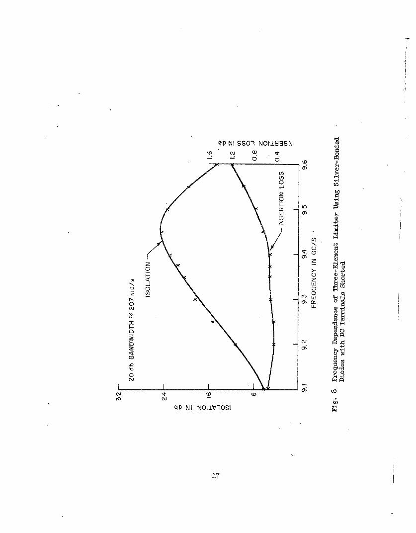
By short-circuiting the diode biasing terminals of the three-elementswitch, a relatively flat limiting characteristic has been obtained. Usingthree silver-bonded diodes, the output power is limited to 1.8 mv for anincident power of 500 Mw CW, as illustrated in Fig. 7. The output character-istic of Fig. 7, -while not perfectly flat, shows an increase of only 0.7'mwin output for an increase in input power from 10 to 500 mw. For the samethree diodes, Fig. 8 depicts the frequency dependence of the limiter showinga peak isolation of 24.6 db with a 20 db isolation bandwidth of 207 Mc/s.The low-level insertion loss at 250 microwatts is less than 0.6 db from9.1 to 9.45 Gc/s rising to 1.2 db at 9.6 Gc/s. Other units have been testedwhich give a low-level insertion loss of less than 1.05 db over the whole
5

band for loss of 1 db in isolation, and a slight narrowing of the 20 db band-width. This case is illustrated in Fig. 9.
A technique, giving limited output power at levels lower than can beobtained with the three-diode limiter just described, is available. This.technique utilizes the rectification properties of the silver-bonded diodewhich is reported to have a rectification ratio of 106.19
The diode first seen by the incident microwave energy, diode A inFig. 10, is inserted in its mount in a direction opposite to the directionof insertion of diodes B and C. The diode terminals are then connected toeach other. Measurements indicate that most of the incident microwave energyis absorbed in diode A, giving rise to a substantial rectified current whichat 500 =-: of input power is as high as 10 nao Since diodes B and C have beeninserted in their respective mounts in a direction of "easy current flow," thecurrent from diode A biases diodes B and C into forward conduction. In thisstate, each diode represents a high impedance and if driven deep enough intoconduction to a point where resonance occurs, the diode impedance can be verylarge. Thus, at increased input power levels (200-600 =,) the large diodeimpedance tends to maintain a low output power level, but not a flat outputcharacteristic.
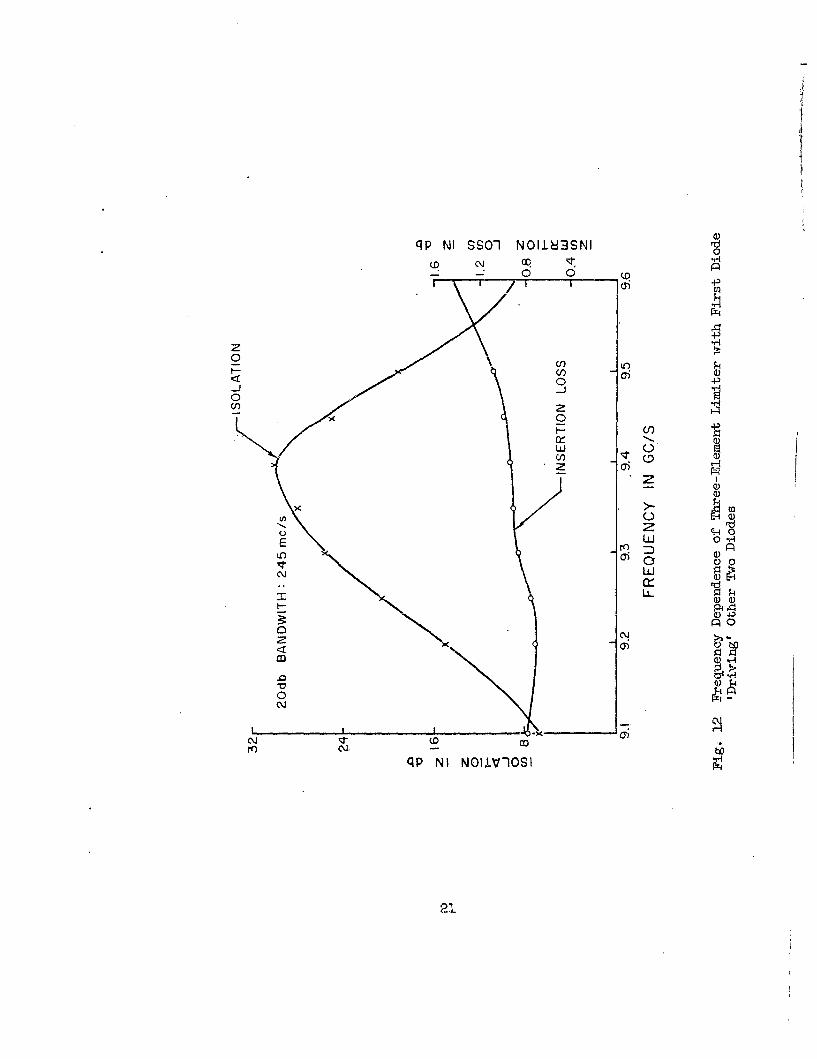
Figure 11 depicts the output characteristic for this type of limiter withthe output power limited to 1.1 mw for 650 mw of input power. The frequencydependence of the limiter is illmstrated in Fig. 12. A peak isolation of30 db with a 20 db isolation bandwidth of 245 Mc/s is shown. The low-levelinsertion loss is less than 1.0 db from 9.1 to 9.45 Gc/s, rising to 1.4 dbat 9.6 Gc/s. This form of the three-diode limiter gives higher peak isolationand broader 20 db bandwidths at the expense of an increased insertion loss.
SUT.NAAY MO CONCLUSIONS
The purpose of this report was to describe a technique for achievingseries mode switching and limiting at X-band, using semiconductor diodes in awaveguide structure. Switching was achieved by the application of forwardand reverse bias -potentials to the diode terminals. When operated as a switch,the three-element configuration provided high isolation and low. insertion loss,using either silver-bonded germanium varactors or silicon junction varactors.The better switching performance, i.e., higher isolation and lower insertionloss over wider bandwidths was obtained using the silver-bonded germaniumdiodes.
The three-element series configuration has also functioned passively asa microwave power limiter. Good limiting action was attained only whensilver-bonded germanium units were used. This can be attributed primarilyto the low voltage at which these diodes enter conduction (aproximately0.3 volt) and the diode parameters which allow resonant operation. The sili-con units enter conduction at approximately 0.8 volt and have higher packagecapacitance, 0.4 :pf, precluding resonant operation in the 9 to 10 Gc/sregion.
If the lead inductance of the silicon units were reduced to 0.7 nano-henries for the same package capacitance of 0.4 W, resonant operation inthe 9 to 10 Gc/s region could be achieved. However, due to the higher con-tact potential of silicon, the threshold of limiting would be higher and theoutput power as a function of input power would resemble tte curve of Fig. 3,
6

in Reference 18.
One of the principal disadvantages of this series mode of operation ispower absorption. Most of the incident microwave power is absorbed withinthe diodes. Thus, for reliable operation, incident power levels must berestricted to levels lower than the dissipation ratings of the particulartype diode being used to prevent diode burnout.
The effect of harmonic generation has not been investigated. It isbelieved that this effect would only become serious in the case of thelimiter at the higher power levels. Thus, if the harmonics were removed by afilter, the isolation at the fundamental frequency would be enhanced.
ACKNOWUMGM S
The author is grateful to the following personnel of USAELRDL:Mr. G. E. Hambleton for guidance and many helpful discussions;Messrs. F. A. Brand and W. G. Matthei for their suggestions and interest;and to Mr. T. Saad and Sage Laboratories for construction of the three-element configuration.
RERENCES
1. D. J. Grace, "Some Applications of Crystal Rectifiers in BroadbandMicrowave Circuits," Microwave Crystal Rectifier Symposium Record,Fort Monmouth, N. J., P. 313, February, 1956.
2. A. Mhlir, Jr., "The Potential of Semiconductor Diodes in High-Frequency Coimzmnications," P-roc. IRE, vol. 46, pp. 1099-1115,June, 1958.
3. M. R. Millet, "Microwave Switching by Crystal Diodes," IRE Trans.on Microwave Theory and Techniques;" volo TT-6, pp. 284-290,July, 1958.
4. R. V. Garver, E. G. Spencer and M. A. Harper, "Microwave SwitchingTechniques," IRE Trans. on Microwave Theory and Techniques,vol. imT-6, pp. 378-387, October 1958.
5. R. V. Garver, "High-Speed Switching of Semiconductors-II,"IRE Trans. on Microwave Theory and Techniques, vol. MTT-7,pp. 272-276, April, 1959.
6. R. Lucy, "Microwave High-Speed Switch," Proc. 1959 ElectronicComponents Conference, Philadelphia, Pa., pp. 12-15, May 6-8, 1959.
7. G. C. Messenger, "A Review of Parametric Diode Research,"Proc. 1959 Electronic Components Conference, Philadelphia, Pa.,pp. 220-222, May 6-8, 1959.
8. C. J. Spector, "A Design Theory for the High-Frequency P-N JunctionVariable Capacitor," IRE Trans. on Ele~ctron Devices, Vol. ED-6,Pp. 347-351, July, 1959.
7

9. R. V. Gerer. J. A. Rosado and E. F. T•Trner, "Theory of theGermanium Diode Microwave Switch," IRE Trans. on Microwave Theoryand Techniques, Vol. NIT-8, pp. 108-111,January, 1960.
10. M. Bloom, "Microwave Switching with Computer Diodes," Electronics,vol. 33, PP. 85-87, January 15, 1960.
ii. A. F. Harvey, "Dup2.exing Systems at Microwave Frequencies," IRETrans. on Microwave Theory and Techniques, vol. MTT 8, pp. 415-431,July, 1960.
12 J. Galejs, "Multidiode Switches," IRE Trans. on Microwave Theoryand Techniques, (Correspondence), vol. IMI'-8, pp. 566-569,September 1960.
13. D. W. Feldman and B. R. McAvoy, "A 100 db Microwave SemiconductorSwitch," Review of Scientific Instruments, vol. 32, pp. 74-76,--January, 1961.
14. S. Kita, J. Okajima and M. Chung, "Parametric Amplifier Using aSilver Bonded Diode," IRE Trans. on Electron Devices, vol. ED-8,pp. 105-109, March, 1961.
15. R. V. Garver and D. Y. Tseng, "X-Band Diode Limiting," IRE Trans.on Microwave Theory and Techniques," (Correspondence), vol. MNT-9,p. 202, March, 1961.
16. R. V. Garver, "Theory of TEM Diode Switching," IRE Trans. onMicrowave Theory and Techniques, vol. MIT-9, pp. 224-238, May, 1961.
17. T. H. B. Raker, "Semiconductor Diode Waveguide Switch," ElectronicTechnology, vol. 38, pp. 300-304, August, 1961.
18. L. Gould, M. Bloom and R. Tenenholtz, "Semiconductor MicrowaveControl Devices," NEREM Record, 1st Edition, pp. 138-139, November,1961.
19. S. Kita, "Microwave Applications of the Silver Bonded Diode,"Electronics, vol. 35, PP. 86-87, l Yay 1962.
20. G. C. Southworth, Principles and Applications of Waveguide Trans-mission, pp. 236-240, D. Van Nostrand Company, Inc., 1950.
8

0
'4-Qr
~ 0 0 0H
r-
00
-H 0 0E-4 M 4 ý
0 * ~ I I
Lrlý \0 a ý
C) ;
-k 4)

Rs "- ZERO' BIAS> Cp
C (v) R
I s I C
L
-0 p FORWARD BIAS
L
R 0 REVERSE BIAS
LCB( V)
Fig. 1 fssumed Diode ,Equivalent Circuits
10

Zg Z0
-E CA ZT
L 0
RFC
SIMPLE SHUNT MODE
RFC
Zg= Zo
{ ZV
SIMPLE SERIES MODE
Fig. 2 Simple Series and Shunt Mode
:1.7

L444
P4-
44
121

48 40db BANDWIDTH; 68 mc/s
30db BANDWIDTH: 170 mc/s20db BANDWIDTH: 258 mc/s
ISOLATION
40-
z /324
_j
0
16 - 1.6 z
1.2 .
0,4u8- 0.8 0
INSERTION LOSS
9.1 9.2 9.3 9.4 9.5 9.6
FREQUENCY IN GC/S
Fig. 4 Typical Switching PerfQrmanee of GSw Type Silver-Bonded Diodes
13

qP NI SS01 N0183SNI
C;.
00
z F
00
U-)0
4-)0
H
00
00
0li LU\IP NINIV1S
z1

qP NI SSO-1 NOIJ63SNI
0D. N~ OD I
00
20 0 -
0) a
0
j'-. ~ D u (D
Cc)C
000 *
.0"0 0 0
qp NI NOI.LV1IOSI
15

0-00
SI
rd
o t
00
0)
3: 0H
00
-o-
z 0
cc
0 0
I-
P.4E
0 •.0
E
af)
0 0 -
SlVMI-1I-IAI NI l3MOd fndJ.NO
qP NI SSO-1 NOIJW93SNI
co
0 to(
0
(U
2 Hrd
0)
0N~j j
09 0
E U2 0)
0) 0)
0 vq3
0 wo
qP NI NOliV1IOSI
17

qP NI SSO-1 NOU83SNI
zN, 0
E Hi
0 -
N cL,
ID3-
z
r') NIN ILV I

101
10
0
P4.
14,

00
00
0
/ -0
.14-1LUi 0 0
CL m
4I-
z
00
00J0-
a)H
oIVIIIV I8Mdidn
IPR
qp NI SSO-1 NOWi3SNI r0
o0 0
*i-
00
U4.
Hrw0
E w 0 HZ2
ai 0 V
N~ u
IL
qP) NI - O I -O IP

DISTRIBUTION LISTCouies Cie
Commanding General 3 Commanding General 1U. S. Army Electronics Command U. S. AzsW SatelliteATTN: A1SEL-AD Communications AgencyFort Monmouth, New Jersey ATTN: Technical Documents
CenterOffice of the Assistant 1 Fort Monmouth, New JerseySecretary of Defense(Research and Engineering) Commanding OfficerATTN: Technical Library U. S. Arxny Engineer ResearchRoom 3E1065, The Pentagon and Development LaboratoriesWashington 25, D. C. ATTN: Technical Documents
CenterChief of Research and 2 Fort Belvoir, VirginiaDevelopmentDepartment of the Army Commanding OfficerWashington 25, D. C. U. S. Army Chemical
Warfare LaboratoriesChief, United States Army 1 ATTN: Technical Library,Security Agency Building 330ALTN: ACofS, G4 (Technical Army Chemical Center, MarylandLibrary)Arlington Hall Station Con-manding Officer 1Arlington 12, Virginia Harry Diamond Laboratories
ATTN: Library, Building 92,Commanding Officer 1 Room 211U. S. Army Electronics Research Washington 25, D. C.and Development ActivityATTN: Technical Library Headquarters, United States 2Fort Huachuca, Arizona Air Force
ATTN: AFCINCommanding Officer 1 Washington 25, D. C.U. S. Army Electronics Researchand Development Activity Rome Air Development Center 1ATTN: SELWS-AJ ATTN: RAALDWhite Sands, New Mexico Griffiss Air Force Base
New YorkCommanding Officer 1U. S. Army Electronics HeadquartersResearch Unit Ground Electronics EngineeringP. 0. Box 205 Installation AgencyM ountain View, California ATIN: ROZýEL
Griffiss Air Force BaseCommanding Officer 1 Ne-w YorkU. S. Army Electronics MaterielSupport Agency Commanding General 2ATTN: SEM13-ADJ U. S. Army Materiel CommandFort Monmouth, New Jersey ATTN: R&D Directorate
Washington 25, D. C.

Distribution List (Cont)Copies Copies
Aeronautical Systems Division 1 Chief, Bureau of ShipsATTN: ASAPRL ATTN: Code 454Wright-Patterson Air Force Base Department of the NavyOhio Washington 25, D. C.
U. S. Air Force Security Chief, Bureau of ShipsService ATTN: Code 686BAETN: ESD Department of the NavySan Antonio, Texas Washington 25, D. C.
Headquarters DirectorStrategic Air Command U. S. Naval Research LaboratoryATTN: DOCE ATTN: Code 2027Offutt Air Force Base, Nebraska Washington 25, D. C.
Headauarters I Commanding Officer & Director IResearch & Technology Division U. S. Navy Electronics LaboratoryATTN: RTH ATTN: LibraryBolling Air Force Base San Diego 52, CaliforniaWashington 25, D. C.
Commander 1Air Proving Ground Center 1 U. S. Naval Ordnance LaboratoryATTN: PGAPI White OakEglin Air Force Base, Florida Silver Spring 19, May•land
Air Force Cambridge Research 2 Comnmander 20Laboratories Armed Services TechnicalATTN: CRXL-R Information AgencyL. G. Hanscom Field ATTN: TISIABedford, Massachusetts Arlington Hall Station
Arlington 12, VirginiaHeadauar"ters 2Electronic Systems Division USAELRDL Liaison Officer IATTN: ESAT U. S. Arnr Tank-Automotive CenterL. G. Hanscom Field Detroit ArsenalBedford, Massachusetts Central Line, Michigan
AFSC Scientific/Technical 1 USAELRDL Liaison Officer 1Liaison Office Naval Research LaboratoryU. S, Naval Air Development Center ATTN: Code 1071Johnsville; Pa. Washington 25, D. C.
Chief of Naval Research 1 USAELRDL Liaison OfficerATTN: Code 427 Massachusetts Institute ofDepartment of the Navy TechnologyWashington 25, D. C. Building 26, Room 131
77 Massachusetts AvenueBureau of Ships Technical 1 Cambridge 39, MassachusettsLibraryATTN: Code 312Main Navy Building, Room 1528Washington 25, D. C. (2)

Distribution List (Cont)Copies Coies
USAELRDL Liaison Office 1 USACDC Liaison Office 2Aeronautical Systems Division SMlRA/LNF., USAELRDLATTN: ASDL--9Wright-Patterson Air Force Base Chief, Technical 6Ohio Information Division
Headquarters, USAELRDLU. S. Ar=U Research Liaison 1Office USAELRDL Technical 1Lincoln Laboratory Documents CenterP. 0 Box 73 SELRA/ADT, HexagonLexington, Massachusetts
Commanding Officer 1
USAELRDL Liaison Officer 1 U. S. ArTiW Security AgencyRome Air Development Center Processing Center, Deal AreaATTN: RAOLGriffiss Air Force Base Chief Scientist INew York U. S, Army Electronics Command
ATTN: AMBEL-SCUSAELRDL Liaison Officer 1 Fort Monmouth, N. J.U. S. Army Combat DevelopmentCommand, CDC12-T-EL Director, Institute for 1Fort Belvoir, Virginia Exploratory Research, USAELRDL
Chief, Bureau of Ships 1 Director, Applied Physics Div., 1ATTN: Semiconductor Group Surveillance Dept., USAELRDL
Code 681Al•, Mr. A.H. YoungDepartment of the Navy Actg. Director, Electronic 2Washington 25. D. C. Components Dept., USAELRDL
USAE7.BA Liaison Engineer 1 Actg. Director, Solid State & 1USASCAJ Frequency Control Div., EC Dept.APO 343San Francisco, California Dep. Director, Solid State & 1
Frequency Control Div. EC Dept.Technical Dir., SELRA/CS 1Headquarters, USAELRDL Chief, Technical Staff, Solid 10
State & Frequency Control Div.USAELRDA-White Sands 1Liaison Office Chief, Piezoelectric Crystal & 10SELFA/LI'M, USAELRDL Circuitry Br., Solid State
& Frequency Control Div.AFSC Scientific/TechnicalLiaison Office Chief, Semiconductor & Micro- 10SELRA/LNA, USAELRDL electronics Br., Solid State
& Frequency Control Div.Corps of Engineers 1Liaison Office Chief, Microwave & Quantum 20SELRA/LNE, USAELRDL Electronics Br., Solid State
& Frequency Control Div.Marine Corps Li.aison Office 1SELRA/UM, USA3LRBDL File Unit Nr. 1, Rm. 3D-j16, 1
Hexagon(3) Axrmy-Ft lonmouthbNJ-MION 1837-63

' 01
~ 1,4~ ~g 1
1 ý. - 1
0--,d
41 .~~ , '
~~4 ilkNo
.
~4 0
INI
g -9 A'
0I~~~~ 00"
.4H
p4gi sc f i~ ~1jAt