unclassified ad 41418(3 - defense technical … ad 41418(3 ... h. device fabrication -diode...
TRANSCRIPT

UNCLASSIFIED
AD 41418(3
DEFENSE DOCUMENTATION CENTERFOR
SCIENTIFIC AND TECHNICAL INFORMATION
CAMERON STATION. ALEXANDRIA. VIRGINIA
UNCLASSIFIED

NOTICE: Nen government or other drawings, speci-fications or other data are used for any purposeother than in connection with a definitely relatedgovernment procurement operation, the U. S.Government thereby incurs no responsibility, nor anyobligation whatsoever; and the fact that the Govern-ment may have foralated, furnished, or in any waysupplied the said drawings, specifications, or otherdata is not to be regarded by implication or other-wise as in any manner licensing the holder or anyother person or corporation, or conveying any rightsor permisiion to manufacture, use or sell anypatented invention that may in any way be relatedthereto.

SECOND QUARTERLY TECHNICAL REPORT
00 Report Date: July 14, 1963ymm.- March 14, 1963 to June 14, 1963
0
"GALLIUM PHOSPHIDE DEVICES"
C5
"..... -CONTRACT NI DA-36.039-AMC-00103 (E)
Placed By:I i iV. S. Army Electronics Material Agency
Vert Monmouth, New Jersey
THE EAGLE.PICHER COMPANY
Chemicals & Metals Division, 11 4
Research Laboratories, nf__ l ,
Miami, Oklahoma f:,AUG 31 Ii .i ,1Il l
TI-ii t

utTANTV -,' 2LAT S , AL L~ DDO04k A't"-'%' 24 111 Jt Q, BL.ACX AND WHIMU
SECOND QUARTERLY TECHNICAL REPORT
Covering the Period
March 14, 1963 to June 14, 1963
Report Date: July 14, 1963
"GALLIUM PHOSPHIDE DEVICES"
Order Number: 5358-PM-63 °91
Date of Contract: December 13, 1962
Amount of Contract: $33,751.62
Contract Numbert DA-36-O39-AmC-00103(E)
Report Prepared by:
Louis E. Stone, J. S. Rodertiqu*,
Jno. E. Budiaelic, GeorS N. Webb,
Lloyd W. Brown.
Edited By:
J. R. Musgrave
The EaSle-Picher Company,Research Laboratories,
Miami, Oklahoma.

TABLE OF CONTENTS
PAGE
1.o PURPOSE# I . . .. . . . . .
Iio ABSTRACT, .. .. . . . . . . . .. . . . . . . . . 2
III. PUBLICATIONS, REPORTS & CONFERENCES, . . . . . . . . 3
IV. FACTUAL DATA:
A. Introduction, .......... . . . . . . . 4Be Synthesis,. .. . . .. .. . . . . 5C. Alternate Synthesis Methods,.. . . . . . . . . . 12Do Melt Grovth,. . . . . . . . . . o . o. . . . . . 17E. Epitaxy Sealed Ampoule, Iodine, . . . . . . . . 19F. Epitaxy Open-Flow, Iodine,. .. . . . . . . . . 23G. Gallium Phosphide Material Evaluation,. .. . . . 26
Electronic, . . . . . . a . . . . . . . . . . . 26Visible Spectrum, o .......... . . . . 26Infrared Spectrum,,.. .. . . . . . .. . 28
H. Device Fabrication - Diode Characteristics$ . . . 30Diffused Diodes ....... ..... . . . . 30Alloyed Diodes, ........ . . . . . . . . . 31Eptaxial Diodes, a. .. .... ...... 32
I. Device Evaluation,.. . . . . . . . . . . . . . . 33Diode Data, . . . . . . . . . . . . . . . # o o o 33
Log I Versus Voltage,. a . . o . .. .o . o 33Junction Positions$ . •.•.. .... . 35
V. S 044ARY, a .# ... .... .... ... 38
VI. FUTURE STUDIES,. . . . . . ..... ... . .. 40
VII. REFERENCES,. . . . . . . . . . . . . ..... . . . 41
VIII. PERSONNEL, . , , ...... . . . • . . .. . . . 42
smuuuu3aunuuuuuuu 88l8J t ist mautR sma
LIST OF TABLES & ILLUSTRATIONS
PAGE
Table I. Summary of Spectre-Analysis GaP, Product, . . . . . . . 6
Table II. Summary of Spectre-Analysis of Phosphorus & Heel, o ... 6
Table III. Gallium Sesquioxide Spectrographic Data,. . . . . . . . . 7
Table IV. Bulk Phosphorus Impurity Spectrographic Data, . . . . . . 7
Table V. Residual Phosphorus Impurity Concentration, . . . . . . . 8
Table VI. Synthesized GaP Impurity Analysis,.. .. . . . . . . . . 9
Figure 1. Gallium Recovery as GaP in Synthesis, . . . . . . . . eo. 10
Figure 2. Photograph Gallium Phosphide Product O-24, . . . . . . . 11
Figure 3. Photograph Gallium Phosphide Product OF-26, . . . , . . . 11
Figure 4. Gallium Trichloride Synthesis Apparatus,. . . . .o. . . 13
Figure 5. Gallium Phosphide Synthesis from Chloride Apparatus,. . . 14
Figi.re 6. Melt Growth Crucible and Shield Assembly,. 9 . . . . # . 16
Figure 7. Iodine Transport Epitaxy System,. ... .. , .. . . . . . 20
Figure 8. Cross Section Epitaxial GaP on GaAs Substrate,. .. . . . 21
Table VII. Surface Resistivity & Carrier Concantration for Sub-strate and Gallium Phosphide Epitaxial Layerso . . . . a 22
Figure 9. Open-Plow Gallium Phosphide Epitaxy System, . . #. o. . . 24
Figure 10. Absolute Transmission of Gallium Phosphide Specimens, . . 27
Figure 11. Infrared Transmission of Gallium Phosphide Specimens, . . 29
Figure 12. Gallium Phosphide Diffused Diode Characteristics, . . . . 30
Figure 13. Gallium Phosphide Alloyed Diode Characteristics,. .. . . 31
Figure 14. Diode Characteristics of Epitaxial GaP on GaAs Diodes,. . 32
Figure 15. Plot In I Versus V of Epitaxial GaP Diodes, . . . . . . . 34
Figure 16. Spectral Response of Epitaxial GaP on GaAs Substrate, . . 36
The work performed under this contract was made possible by
the support of the U. S. Army Electronic Materiel Agency,
Fort Monmouth, New Jersey.

I* PURPOSE
The purpose of this investigation is the growth of single crystal gal-
lium phosphide suitable for device applications; the evaluation of such mat-
erial, and the fabrication of appropriate devices.
The materials category includes the selection of a suitable synthesis
process, growth of single crystals of best purity, and refinements in tech-
nique for optimum purity, stoichiometry and crystalline structure. Suitably
doped n-type and p-type gallium phosphide is considered a principal object-
ive.
The evaluation program includes the analysis of impurity concentrations,
measurement of resistivity, Hall mobilities and similar electronic parameters.
Optical properties such as transmittance, absorption, and electrolumLnescence
are included.
The fabrication program is aimed primarily at single junction diode
structures, although three terminal devices are contemplated as a logical
extension in evaluating the junction parameters. Device parameters of interest
include contact ohmicity, I-V rectification properties, temperature perform-
ance, junction luminescence and photovoltaic effects. Three terminal evalua-
tion in terms of transfer characteristics is considered an objective. Further
parameters of special interest will be carried out when considered useful by
the Government Contracting Officers Representative.
- I-

11, ABSTRACT
The synthesis of gallium phosphide has been improved in purity
of product, recovery efficiency, and reproducibility. Careful con-
trol of process temperatures and flow rates has been a major factor
in this improvement and exploits the inherent purification of the
phosphorus. Alternative vapor synthesis systems have been explored
without practical success.
The melt growth was impeded by furnacing difficulties, which
have been r6solved, and melt growth studies are being pursued.
Epitaxial growth of gallium phosphide layers of superior quality
has been accomplished using iodine transport in both sealed ampoule
and open-flow techniques. The latter offers significant advantages
in facilitating alternate type growth and close control cf thickness.
Diffused, alloyed and epitaxial gallium phosphide diodes have
been fabricated and tentative evaluation carried out. Some resistive
effects were observed, and are considered principally the effect of
material properties.
Evaluation of optical properties of early bulk gallium phos-
phide material has been carried out. Results closely agree with theo-
retical physical properties.
- 2-

III. PUBLICATIONS. REPORTS AND CONFERENCES
Reports:
Monthly Letter-Type Report No. 3 was prepared and delivered on 4/20/63,
Monthly Letter-Type Report No. 4 was prepared and delivered on 5/16/63.
Conferences:
A conference was held at Fort Mormouth, New Jersey, on May 23, 1963.
Present were Messrs. Robert Yatako, Phillip Newman and James Kesperis, of
Evans Laboratory, and Mr. Louis E. Stone of this laboratory. The subject of
the conferences was the current progress of the investigation, and delivery of
the following samples:
16305-AZ - Epitaxial GaP on GaAs Substrate EG-36-2M6305-BA - Epitaxial GaP on GaAs Substrate EG-35-2146305-BB - GaP diode ELGD-2-1
A conference was hel-d at the Eagle-Picher Laboratory, Miami, Oklahoma,
on June 5 & 6, 1963 with Mr. Robert Yatsko of Fort Monmouth, New Jersey. The
techniques for open-flow gallium phosphide synthesis, melt-growth of crystals,
epitaxial growth, chemical polishing, microscopic measurement, etc., were dem-
onstrated in detail. A comprehensive discussion of purpose and guidelines for
the investigation was held and current progress and problems discussed.
Specimen 146306-AT, polished cross-section of an epitaxial gallium phos-
phide layer on gallium arsenide substrate was delivered to Mr. Yatsko.
- 3 -

IV. FACTUAL DATA
A. Introduction:
Satisfactory progress has been made in the open-flow gallium phosphide
synthesis phase during this period. As will be detailed subsequently, pro-
duct purity levels have been improved; reproducibility from run-to-run has
been steadily increased; less variation in yield is noted, and use of less
pure phosphorus without increased contamination has been possible by careful
control of its sublimation temperature.
Several alternate synthesis techniques have been explored briefly, with
little success. These were planned to use vapor sources for both the phos-
phorus and gallium, reacted in a high temperature zone. Both produced very
low yields and were judged impractical.
The melt growth phase was temporarily impeded during this period. The
thermal insulation in the high temperature furnace was replaced with a better
material. The improved properties of this new and different insulation has
produced a quite sharp temperature gradient within the melt zone, and made
necessary a series of test runs to establish the proper temperature and pull
rates. Several unsuccessful runs were made before it became apperent that an
increased vertical temperature gradient existed. Orderly and logical tests
have now been made, and tentative operating parameters have been established.
It is considered that melt grown ingots of good crystal structure will be
forthcoming soon.
Slices of melt grown ingots have been used for evaluation and devices.
This material is of multi-crystalline nature, undoped, and of low net
- 4 -

$on" carrier concentration* Spectral transmittance and infrared absorption
data are included as part of this report.
The device fabrication phase has proceeded satisfactorily. Principal
effort has been on epitaxial growth of Sallium phosphide layers on gallium
arsenide substrates, and a small numberof bulk gallium phosphide alloyed
diodes. The epitaxial growth has included "n" gallium phosphide on "n" gal-
lium arsenide, and "p" gallium phosphide on "n" gallium arsenide. Clear
single crystal layers of from eight to eighty microns thickness have been
grown. Significant photovoltaic measurements have been made on some of
these specimens.
B. Gallium Phosphide Synthesis*:
The synthesis of gallium phosphide is accomplished by the open-flow
technique, described in detail in the First Quarterly Report(l). Briefly
stated the method involves passing elemental phosphorus vapor over gallium
sesquioxide at an elevated temperature, using hydrogen gas as a carrier.
The quartz environment gives rise to the principal contaminant, silicon.
The Ga203 used is high purity material, obtained from the Eagle-Picher
Company. Total impurities range from 0.7 FFM to 1.01 PPM, of which the
major component, silicon, ranges about 0.5 PPM.
Original synthesis runs1indicated very high phosphorus impurities
were present and were carrying over into the final product. Very high purity
phosphorus was obtained (1.0 PPM total), and sublimation temperatures care-
fully controlled. Spectrographic analyses of twenty-two runs made during
* This phase of the work was performed by J. S. Roderique.
- 5 -

the first quarter are suumarized in Table I,
TABLE I
Sumary of Spectrographic Analysis (Previous)Total
Impurities in Parts Per Million Lmpurities (PPM)
si MR. Fe. Al Cu Ca
GaP av. Imp* 50,0 3.0 1.0 2.0 1.0 10.0 67.0
Best (OP-15) 7.0 3.0 N.D. 2.0 N.D. N.D. 12.0
NOIE: "N.D." - None Detected.
The inherent purification obtained in subliming the phosphorus under
careful temperature control was observed by analysis of total phosphorus
impurities before use, and analysis of the heel remaining after terminating
a run. This effect is illustrated for high purity phosphorus in Table II,
as noted in the First Quarterly Report.
TABLE II
Summary of Spectrographic Analysis of Phosphorus and Heel.
Total PPM Before Total PPM
Phosphorus Run Number Sublimation Heel
Fisher, OF-8 7 x 10 5 2 x 10 5
AACC Q-004, OF-11 N.D. 6.0
MACC Q-003, OF-13 0.5 10.5
AACC Q-003, O1-15 0.5 100.0
NOTE: "N.D." - None Detected.
The inference of these data was that careful control of sublimation
temperatures should improve final product purity and/or allow use of less
pure phosphorus. During this quarter more exploration was carried out to
clariij this factor.
.6-

Impurity levels in starting materials was carefully monitored by spec-
trographic analysis throughout this work period. The Ga203 used was Eagle-
Picher high purity semiconductor grade, with impurities as illustrated in
Table III.
TABLE III
Gallium Sesquioxide Spectrographic Data.
.murities - in Parts Per Million
Eagle-PicherLot Numbers Pb Cu Fe MR Ca TOTAL
137.3, 0.10 0.36 0.10 0.007 0.33 0.977I.Q - 869, 0.10 0.36 0.10 0.087 0,33 0.977
Phosphorus purity is defined in Table IV. Note that a wide difference exists
in bulk impurities. These lots of phosphorus were fresh lots, stored in seal-
ed containers in inert atmosphere.
TABLE IV
Bulk Phosphorus Impurity "pectrographic Data.
Impurities - in Parts Per MillionTOTAL
Phosphorus Si -M Al Cu A& Ca Na PPM
AACC Lot Q-005, 20.0 2.0 50.0 1.0 5.0 20.0 N.D. 53.0AACC Lot Q-023, 5.0 N.D. N.D. NeD, 5.0 2.0 N.D. 12.0Fisher, 701504, 20.0 3.0 5.0 0.5 0.5 500.0 50.0 579.0
NOTE: "ND." = None Detected.
A surplus of fresh phosphorus was used each run, and a generous heel left at
the termination of the run. This residue was analyzed spectrographically to
indicate any buile-up in impurity concentration. Results, indicated in
Table V, were in agreement with the earlier work, and show a remarkable in-
crease.
-7"

Residual Phosphorus Impurity Concentrations.
Inurities - Parts Per Million
Reference Run Phosphorus Total PPM Total PPMNumbers Numbers Identity Before Sublimation Residual Heel
M6304-AE OF-25 Fisher #1, 1.1 x 10⁴ 1.3 x 10⁵
16304-BH O7-26 Fisher #2, 500 1.1 x 10³
M6304-BI 0F-27 Fisher #2, 500 2.1 x 10⁴
16304-BK 0F-28 Fisher #2, 500 1.35 x 10⁴
M6305-AR OF-29 Fisher #2, 500 1.1 x 10⁴
H6306-BI 01-30 Fisher #2, 500 2.6 x 10⁴
M6306-BJ 0F-32 Fisher #2, 500 2.7 x 10⁴
M6306-BW 0F-33 Fisher #701504, 579 7.8 x 10⁴
It is evident from these data that the sublimation of phosphorus at
restricted, controlled temperatures (below 400*C) left the major contam-
inants in the residue. The next consideration is to what degree this ef-
fect is reflected in product purity. Table VI indicates results of spec-
trographic analysis of the gallium phoaphide product. In each case, the
product was crushed, mixed and sampled, rather than sampling preferenti-
ally the needle formation. Thus these data represent overall purity,
- 8 -

TABLE VI
Synthesized GaP Impurity Analysis.
Impurities - in Parts Per Million
•GaP Run Si MR Al Cu Ca TOTAL - PPM
0F-23 20.0 3.0 7.0 0.5 5.0 35.5
0F-24 30.0 5.0 5.0 1.0 5.0 46.0
0F-25 20.0 5.0 2.0 1.0 5.0 33.0
0F-26 50,0 3.0 N.D. N.D. 10.0 63,0
OF-27 30.0 3.0 N.D. N.D. 10.0 43.0
0F-28 50.0 3.0 N.D. N.D. 5.0 58.0
oF-29 20.0 5.0 N.D. 1.0 5.0 31.0
* -31 300.0 3.0 2.0 1.0 10.0 316.0
OF-32 5.0 3.0 2.0 0.5 10.0 20.5
0-33 30.0 3.0 2.0 1.0 10.0 46.0Avrage,excluding #31,equals,
28.0 3.6 2.0 0.5 7.0 41.8
NOTE: * - This run was a sintering of 01-12, 14-A, and 01-30 material.(Sintered 1000C - 4 hours under helium, 1000C - 2 bra. underhydrogen). This explains the relatively high build-up of sil-icon.
"N.D." - None Detected.
It is of interest to compare the average values of Table VI with those
of Table I, which were carried out the previous quarter using high purity
phosphorus with less stringent restriction and control of temperature. The
overall average impurities of this quarter are at least as good, It is con-
sidered subsequent runs with the higher purity phosphorus will benefit from
this study by a further decrease in impurities, with the possible exception
of silicon.
-9-
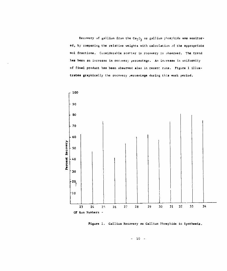
Recovery of gallium from the Ca2 %3 as gallium pbosphide was monitor-
ed, by comparing the relative weights with calculation of the appropriate
mol fractions. Considerable scatter in recovery is observed. The trend
has been an increase in recovery percentage. An increase in uniformity
of final product has been observed also in recent runs. Figure 1 illus-
trates graphically the recovery )ercentage during this work period.
100
90
80
70
60
50o 50U
-40
3o
-20
-10
23 24 2 26 27 28 29 30 31 32 33 34
OF Run Numbers -
Figure 1. Gallium Recovery as Gallium Phosphide in Synthesis.
- 10 -

Typical GaP product is illustrated by Figure 2 and Figure 3. The directionof H2 flow may be inferred by the dendritic needle growth. Particular noteis made of the uniform color.
Figure 2. Photograph of Gallium Phosphide Product of (1-24.
Figure 3. Photograph of Gallium Phosphide Product of OF-26.
Some improvements in apparatus is being incorporated currently, and are ex-
pected to improve both control and product quality.
- 11 -

C. Alternate Synthesis Methods:
The open-flow system previously described is adequate in general, yet
leaves something to be desired in (a) volume per run, (b) density of pro-
duct, and (c) segregation of residues apd by-products. Volume of charge
is not easily scaled up over 25 grams, without traces of residual unreact-
ed Ga203 . Product density is that of a semi-compacted powder; crystalline
aggregate material would be preferable. To prevent inclusion of adsorbed
phosphorus, gallium monoxide and other phases, the product and boat are
sintered briefly before and after reaction, which reduces the net yield of
gallium phosphide.
Thus some exploration of a vapor-vapor reaction was contemplated,
which might produce crystalline-aggregate material, and eliminate several
of the problems mentioned. Three alternates were suggested and carried out.
The first employed gallium trichloride and phosphorus trichloride; the sec-
ond gallium trichloride and elemental phosphorus vapor; and the third gal-
liub triiodide and elemental phosphorus vapor.
Gallium Trichloride and Phosphorus Trichloride Method:
Since high purity gallium chloride is not available commercially, it
was synthesized in our own laboratory. The apparatus used for this purpose
is illustrated in Figure 4. A 25-mm quartz tube, horizontal at one end, was
arranged to have a sump near its middle, to which a quartz receiver was weld-
ed. Chlorine gas, suitably metered and dried, was passed over a quartz boat,
containing high purity gallium, which was located in the horizontal section.
Appropriate scrubbers, and exhaust apparatus completed the gas train.
- 12 -

Figure 4. Gallium Trichioride Synthesis Apparatus.
The trichioride synthesis procedure is as follows:
A smsall quartz boat containing 99.9999 percent p,.- elemental gallium is
positioned in the upstream '%.ri~ontal portion of the reaction tube. The
unit was purged with dry chlorine gas for 30 minutes, the flow was adjust-
ed to a slow rate (0.5 LPM) and heat applied with a gas burner to the gal-
lium boat. The reaction, once started, was exothermic and continued after
heat was removed until synthesis was comple~ted.
- 13 -

The synthesized gallium trichloride solidified on the downward portion
of the reaction tube and was liquefied with a small amount of heat. It was
then collected in the quartz receiver.
There was some free chlorine occluded in the gallium trichloride pro-
duct. The chlorine gas was replaced with helium and at this time the tri-
chlorine product was warmed until liquid, releasing the free chlorine. The
trichloride receiver was cut free, sealed and stored until used for gallium
phosphide synthesis.
The first effort at synthesizing gallium phosphide from gallium and
phosphorus trichloride was carried out in the apparatus pictured below in
Fixure 5.
Figure 5. Gallium Phosphide Synthesis - From Chloride Apparatus.
- 14 -

The synthesis system consisted of induction heating of a graphite sub-
str~te to 600"C (subsequently to 800"C), resistance heated individual GaCl 3
and PCI3 boilers, appropriate drying of helium carrier gas, and suitable
scrubbers and exhaust for tail gases. Total helium flow was measured,
(0.5 LPM) and then divided and passed through H2SO4 bubblers to their res-
pective boilers.
After purging for 30 minutes, helium gas flow was adjusted and the
graphite substrate was raised to 600"C. The two chloride boilers were raised
20"C above the boiling points, and the vapor streams combined before passing
over the heated substrate. After 30 minutes running time, the process was
halted and results observed. Some synthesis had occurred, but the reaction
GaCl3 + PC 3 GaP + C12
appeared heavily unbalanced toward the left at this temperature, resulting
in only a small quantity of gallium phosphide.
Considering the possibility of CC14 formation from the graphite sub-
strate, it was enclosed in clear quartz and the experiment repeated. Results
were essentially the same. A third trial was made at 800"C substrate temper-
ature, which resulted in a smaller quantity of gallium phosphide product.
Gallium Trichloride and Phosphorus Method:
Since the by-product chlorine concentration was considered to weight the
reaction equilibrium toward the left, a reduction would enhance the feasibil-
ity of the process. Thus, elemental phosphorus vapor was substituted for the
PCI 3 vapor and the 600"C experiment ran again. Results indicated more gallium
- 15 -

phosphide synthesis and product, but still far too little to be satisfactory.
It was considered that the rate of attack of chlorine would increase
with temperature, yet the synthesis rate might be even greater with increas-
ed temperature, and a re-cycling technique at higher temperatures could ac-
complish efficient conversion. In the interest of completely exploring this
method, a revised apparatus was constructed, incorporating a 10-inch long re-
action zone, capable of 1100"C operation. Experimental runs were carried out
at 600*C, 800*C and 1075*C. The product quantity increased, but was too
little to be practical as a synthesis process.
Gallium Ttiiodide and Phosphorus Method:
The vapor synthesis from gallium triiodide and elemental phosphorus was
explored similarly to the trichloride. The gallium triiodide was prepared
in the same manner, and gallium phosphide synthesis carried out at 600 0CD
800"C and 1050*C. Results closely paralleled that of the chloride method;
recovery quantity was very small in each case.
Effort in use of this specific vapor series has been suspended; other
vapor techniques will be considered on their merits, and explored briefly
when considered feasible.
- 16 -

D. Melt Growth*:
The gallium phosphide melt growth phase ran into serious difficulties
early in this work period. These difficulties have been primarily due to
a change from Alfrax insulating material in the furnace, to an improved
graphite insulation. The old insulation had become saturated with vapor
products and physically deteriorated to the degree that replacement was man-
datory. It is worthy of note that temperatures in excess of 2000*C and pres-
sures of 50 atmospheres for periods of hours are routine in this equipment.
Previous to the change of insulation, temperature calibration indicat-
ed a broad vertical gradient existed in the heater, peaking approximately
at the center of the heater. Temperature is measured at this height by a
graphite-graphite thermocouple located between the crucible and the heater
walls. Thermocouple output is measured by a recorder, and has been correl-
ated to power input with fairly good reproducibility.
Initial melt calibration with the new insulation agreed rather well
with temperatures recorded and power input. However, first serious melt
runs resulted in crucible failure, apparently due to excessive temperature.
Runs with incrementally decreasing temperature immediately indicated malting
was not accomplished below the temperature at which crucible failure had oc-
curred.
Resolving this anomaly was a rather slow process. The study establish-
ed the existence of a rather sharp temperature peak of the order of 200°C
greater than that observed at the thermocouple location. The effect of the
excessive temperatures are illustrated in Figure 6, where the tungsten car-
bide outer shield is observed to have softened end swelled at the base.
* The work on this phase was performed by Lloyd W. Brown.
- 17 -

Figure 6. Melt Growth Crucible and Shield Assembly.
The net effect of this temperature differential was to produce either
incomplete melting, or ingots in which cooling rates from the melt were so
excessive that micro-granular structure resulted. It is of interest to note
that these difficulties were not peculiar to the material. Similar effects
were noted in the melt growth of cadmium sulfide crystals in a different in-
house study.
Correction of this problem was accomplished by a change in thermocouple
location and re-calibration runs or, known melting point materials. Currently,
melt growth has begun, with incremental temperature increases beginning at a
temperature just below the melcing point of gallium phosphide to establish
the proper temperature and pull rates to obtain good crystal structure.
- 18 -

A total of sixteen melt runs and twenty calibration runs were carried
out during this period. Of the melt runs, four produced usable material,
eight were of micro-granular structure or unmelted, and four ruptured dur-
ing furnacing and decomposed.
Indicating the acquisition of control, the last melt growth run pro-
duced a fully melted, transparent ingot of 4-grams weight, of good crystal
structure. Strenuous effort is being exerted and the prognosis of rapid
progress in this phase appears reasonable.
E. Epitaxy: Sealed Ampoule Iodine Transport.
Epitaxial growth of gallium phosphide on gallium arsenide substrates
has been carried out by two methods. Mthod #l is of the sealed ampoule
type, using iodine as the transport vehicle. Typical apparatus is shown
schematically in Figure 7, Source temperature was 10000C, substrate tem-
perature 750*C, and growth was carried out for periods of 30 minutes, 1 hour,
and 2 hours. Results were very good. Layers of 8 to 60 microns thickness
were observed and measured. Figure 8 illustrates the transparency of such
a layer approximately 20 microns thick, when observed microscopically with
the specimen illuminated from the side. Some polishing damage was observed
at the interface in this specimen. This may be due to the differential hard-
ness of the two materials, or may be the result of the small difference in
unit cell dimensions producing dislocations along the interface. The affect
of any such defects, if present, do not appear serious in preliminary device
applications, as will be discussed later.
* The work on this phase was performed by John C. Budiselic.
- 19 -

A4 0 .4 M : ia.. 0.i ( 1i
0 &A4 a .4 3 - 0
0.
114
200

Figure 8. Cross-Section Epitaxial Gallium Phosphide on GalliumArsenide Substrate.
Surface conditions of such epitaxial layers were carefully observed
in forty-nine specimens. Initially, attack and erosion of substrates with
subsequent irregularities of the grown layer was observed. This was con-
sidered the result of early attack by the iodine vapor, aggravated by sim-
ultaneous heating of source and substrate. A technique was evolved where-
by the iodine and source reaction was initiated first at 900*C, with the
substrate temperature at approximately 500 degrees for a short period, pre-
liminary to placement at the fixed, high temperature zones in furnacing.
Improved results were obtained, with recent surfaces remaining very
smooth and highly reflective, changed only in color to a grey appearance.
- 21 -
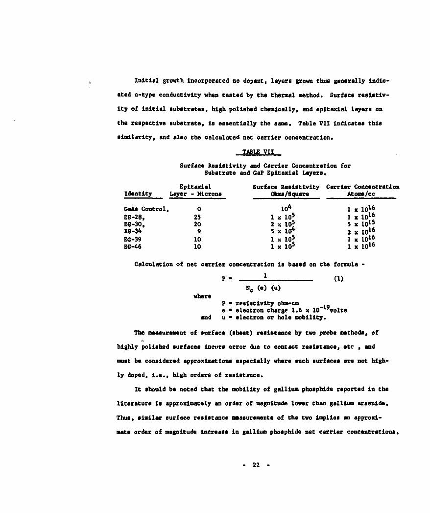
Initial growth incorporated no dopant, layers grown thus generally Indic-
ated n-type conductivity when tested by the thermal method. Surface resistiv-
ity of initial substrates, high polished chemically, and epitaxial layers on
the respective substrate, is essentially the same. Table VII indicates this
similarity, and also the calculated net carrier concentration.
TABLE VII
Surface Resistivity and Carrier Concentration forSubstrate and GaP Epitaxial Layers.
Epitaxial Surface Resistivity Carrier Concentrat-LonIdentity Layer - Microns Ohms/Square Atoms/cc
GaAs Control, 0 104 1 x 10¹⁶
EG-28, 25 1 x 10⁵ 1 x 10¹⁶
EG-30, 20 2 x 10⁵ 5 x 10¹⁵EG-34 9 5 x10⁴ 2 x 10¹⁶EG-39 10 1 x 10⁵ 1 xlO 16
EG-46 10 1 x10⁵ 1 x 10 1 6
Calculation of net carrier concentration is based on the formula -
p 1 (1)
Nc (e) (u)where
P - resistivity ohm-cma W electron charge 1.6 x 10 19volts
and u - electron or hole mobility.
The measurement of surface (sheet) resistance by two probe methods, of
highly polished surfaces incurs error due to contact resistance, ate , and
must be considered approximations especially where such surfaces are not high-
ly doped, i.e., high orders of resistance.
It should be noted that the mobility of gallium phosphide reported in the
literature is approximately an order of magnitude lower than gallium arsenide.
Thus, similar surface resistance measurements of the two implies an approxi-
mate order of magnitude increase in gallium phosphide not carrier concentrations.
- 22 -

Stated differently, for a given similar carrier concentration, an order of
magnitude greater surface resistance would be expected, General agreement
with this principle has been observed in these measurements,
Epitaxial growth of p-type gallium phosphide layers on n-type gallium
arsenide substrates was carried out similarly, using a few milligrams of zinc
iodide as both the transport vehicle and dopant. Layers of 10 to 50 microns
thickness were grown. Typing by thermal methods indicated consistently p-type
conductivity. Surface resistances ranged in the order of 104 ohms per squareindicating carrier concentration of the order of lO1 7atoms per cm3 . Signif-
icant diode and photo parameters were observed in these structures and are
described subsequently.
P. Open-Flow Iodine Epitaxy:
The use of an open-flow system was considered desirable and feasible,
and offered significant advantages where growth of alternate conductivity
type layers with abrupt transition were desired. The system is diagramed
in Figure 9. Elemental iodine, vaporized by a constant temperature water
bath is carried by hydrogen gas over a source/charge of gallium phosphide
at 1000C where reaction occurs. The reaction products migrate gently down
a temperature gradient and pass over the 750"C gallium arsenide substrates,
disproportionating and growing epitaxially on the substrates. By-products
are exhausted through suitable traps.
- 23 -

04
OA
0.o
-- d
24 U

The gallium phosphide source, contained in a boat, is arranged to allow
insertion and/or removal from the 1000"C zone, as is also the substrate
platform. After purging, an atmosphere of hydrogen is established, the
substrates inserted for in-situ cleaning. The iodine flow and insertion
of source is begun simultaneously, and growth carried out for the prescrib-
ed time. The source is removed to a cool portion of the tube, iodine flow
terminated and hydrogen used to sweep out residual vapor products. (At this
point a gallium phosphide charge/source of opposite conductivity type dop-
ing may be inserted and continued growth carried out without distrubing
the system integrity, and with minimum time between growth).
Undoped layers of 10 to 25 microns thickness were successfully grown
using this system. Results in each case were equal, or superior, to the
sealed ampoule method, and eliminate sealing and pumping operations with
consequent saving of time and materials. Surfaces were excellent; uniform
in thickness and very smooth. The requirements for reverse growth, i.e.,
gallium arsenide on gallium phosphide substrates, are less stringent, and
exploratory runs indicate this system is excellently suitable for it. Dis-
cussion of this application will be made subsequently under "Device Fab-
rication".
- 25 -

0. Gallium Phosphide Material Evaluation:
Electronic.
The evaluation of the electronic parameters has been inhibited for
lack of large single crystal specimens. Specimens obtained from melt growth
ingot #M-9, with possible grain boundaries, were measured as indicated below:
Specimen: M6303-DR Ingot M-9Resistivity: 2 x 10³ ohm-cm 14 3Net Carrier Concentration: 10 stome/cm.
It is considered probable that grain boundaries do exist in this spec-
imen and the indicated resistivity is higher then actual. Other specimens
are in process and will allow more exact determination.
Visible Spectrum.
Since one device application of this material will involve signal trans-
mission in the form of light, optical transmission data are of interest. Two
specimens were selected, polished and measured. A Bausch & Lomb Spectro-
photometer was used, with resolution of 100 A. Subsequently the same spec-
imens were measured with a Beckman DU instrument, with resolution of 5 A*.
Excellent agreement was obtained, particularly in the band edge region.
Figure 10 illustrates the transmission data. Specimen M6306-AZ, approxi-
mately 1-rn thick, from melt grown ingot #M-10, was a cross section slice.
Specimen 146306-BA, 3.0-rm thick, was a cross section slice of a vapor grown
plate.
- 26 -

100
80
60
40
2 0
500 550 600 650 '00 750 800 850
Figure 10. Aboulute Transmistlan of C.liun Phosphide' Specimens.
- 27 -
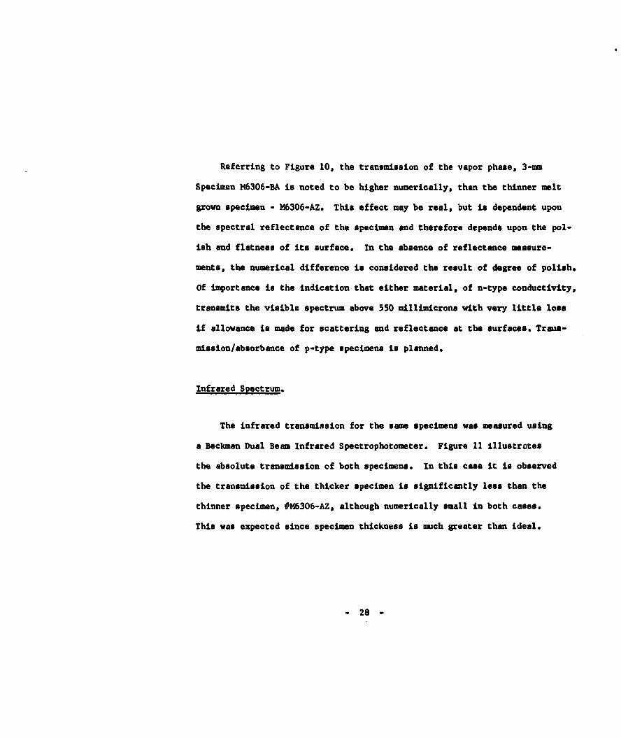
Referring to Figure 10, the transmission of the vapor phase, 3-amm
Specimen M6306-BA is noted to be higher numerically, than the thinner melt
grown specimen - 86306-AZ. This effect may be real, but is dependent upon
the spectral reflectance of the specimen and therefore depends upon the pol-
ish and flatness of its surface. In the absence of reflectance measure-
ments, the numerical difference is considered the result of degree of polish.
Of importance is the indication that either material, of n-type conductivity,
transmits the visible spectrum above 550 millimicrons with very little loss
if allowance is made for scattering and reflectance at the surfaces. Trans-
mission/absorbance of p-type specimens is planned.
Infrared Spectrum.
The infrared transmission for the same specimens was measured using
a Beckman Dual Beam Infrared Spectrophotometer. Figure 11 illustrates
the absolute transmission of both specimens. In this case it is observed
the transmission of the thicker specimen is significantly less than the
thinner specimen, #M6306-AZ, althcugh numerically small in both cases.
This was expected since specimen thickness is much greater then ideal.
- 28 -

.
A
--4
' I.
04
U
&J E
q
iV
I ! ! !0 0 G C' 04
- 29 -

H. Device Fabrication;
Diodes of both diffused and alloyed structure were fabricated. Perti-
nent data is detailed below for the zinc diffused gallium phosphide diodes
fabricated thus far.
Bulk GaP Resistivity = 2 x 10³ ohm-cm (M-9)Bulk GaP Carrier Concentration - 1015 atoms/cm
3
Final Surface Preparation = Chemically polished methyl alcohol+ chlorine.
Zinc Diffusion - 800"C- 15 Min. Sealed ampoule.Bottom (n) Contact - In, Sb, Sn Alloy.Top (p) Contact - Pb-Cd Alloy.
The diode characteristics of these diodes, made by Tektronix #575 Curve
Tracer, are illustrated in Figure 12. The characteristic indicates consider-
able resistance in forward slope, and is considered the effect of the undoped
high resistivity bulk material. The diode results reported here are tentative,
and will be more precise and informative when doped single crystal material is
avsilaLie.
so
60
40
20
223
(volts)20
Figure 12. Gallium Phosphide Diffused Diode Characteristic&.
30
Alloyed Diodes.
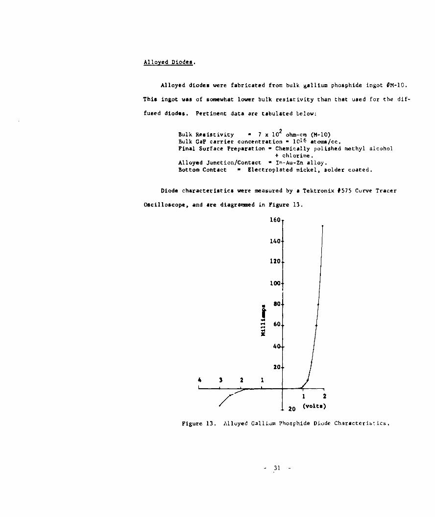
Alloyed diodes were fabricated from bulk gallium phosphide ingot #M-10.
This ingot was of somewhat lower bulk resistivity than that used for the dif-
fused diodes. Pertinent data are tabulated below:
Bulk Resistivity = 7 x 10² ohm-cm (M-10)Bulk GaP carrier concentration = 1016 atoms/cc.Final Surface Preparation - Chemically polished methyl alcohol
+ chlorine.Alloyed Junction/Contact - In-Au-Zn alloy.Bottom Contact = Electroplated nickel, solder coated.
Diode characteristics were measured by a Tektronix #575 Curve Tracer
Oscilloscope, and are diagrammed in Figure 13.
160
140,
120
1001
iS0
- 60..4X
4(
20.
4 3 2 1
1 2
20 (volts)
Figure 13. Alluyed GalliUm PhosFhide Diode Characteristics.
31 -

Epitaxial Diodes.
Epitaxial growth of p-type gallium phosphide on n-type gallium arsen-
ide substrates was carried out to explore the possible difficulties or pec-
uliarities in junctions where the possibility,or even probability, of self-
diffusion exists. Epitaxy was done by the sealed ampoule, zinc iodide trans-
port method previously described. Two milligrams zinc iodide were used, pro-
ducing low order doping.
Surface resistivity by 2-probe methods indicated zinc carrier concen-
tration to be approximately 1016 to 1017 atoms/cm3 . Contact to both "p" and
"n" surfaces was made with electroplated nickle and solder coating. Mesas
were etched and individual diodes scribed, separated and mounted on TO-5
transistor mounts. Typical data for these diodes are illustrated in Figure
14.
100
80 j...... ]KG-Al-2
60
40
20
10 9 8 7 6 5 4 3 2 1
(volts)
Figure 14. Diode Characteristics of Epitaxial Gallium Phosphideon Gallium Arsenide Diodes.
- 32 -
I. Device Evaluation:
Device fabrication studies have just begun; thus the evaluation results
given here are tentative and of an indicative nature. The diode response for
diffused junction gallium phosphide devices (Fig.12) indicate considerable
forward resistive effects. This series tR11 may be composed of bulk resist-
ance, contact resistance, sheet resistance in the diffused layer, and/or
grain boundary barriers. Surface (sheet resistance) measurements indicate
fairly high values, which implies low carrier concentrations to be one of
the principal factors* Bulk resistivity of material is also considered a
contributing factor, since the material was not doped in growth, Low re-
sistivity, doped material presumably will be available soon for diode fab-
rication.
The alloyed diodes (Fig.13) indicate better characteristics, and to a
degree corroborate the above cantention. Lower bulk resistivity material was
used; the alloy re-grown junction gave significantly higher p-type conduct-
ion. Resultant diode curves have much steeper forward slope.
The epitaxial gallium phosphide diodes (Fig.14) were grown using two
milligram of zinc iodide, now considered less than sdould be used for ade-
quate doping. Some resistive slope is observed in these diodes; bulk resist-
ance and low doping levels are considered responsible. The layers were grown
for epitaxial studies per se; subsequent layers will be heavily doped for
device applications. Some insight into doping concentrations can be obtained
from a plot of In I versus V of a diode. The slope, d(qv/kt)/d In I of a
conventional, heavily doped semiconductor junction in the straight line po-
tion, has a value of 2.0 or more. Plots were made of several of the epitax-
ial gallium phosphide on gallium arsenide diodes. Typical of these is Fig-
ure 15.
- 33 -

10
1. AMo Ic 2
.1
.01 I i
.1 .2 .3 .4
Volts
Figure 15. Plot in I versus V of Epitaxial Gallium PhosphideDiodes.
The al-ope indicated was between 1.0 and 1.5 for several such diodes.
The inference is of a graded junction, or one in which the doping gradient
is not abrupt. It is expected that this slope will be increased signifi-
cantly with increased acceptor doping during growth. Cognizance is taken
of an alternative, e.g., heterojunction rectification, where only a simple
barrier lowering mechanism is involved. This alternative appears unlikely,
since definite type change was observed by thermal typing.
Photovoltaic measurements were made of several epitaxial "p" gallium
phosphide on "n" gallium arsenide wafers, previous to ass etching. The
object here was to ascertain, if possible, to what degree diffusion of zinc
carriers into the gallium arsenide substrate was iccurring. Due to the
- 34 -

difference in band gap, it is considered that a Voc in excess of 1,0 volt
might be observed where a good p-n junction is made in gallium phosphide.
This value is considerably more than a similar gallium arsenide junction
might produce. Also, in the first case, a significant increase in spectral
response in the blue region might be observed.
Voc was measured with a plated contact on the bottom of each specimen,
and a point probe to the surface. Maximuam Voc measured is listed for each
type of device.
Zinc Diffused Gallium Phosphide Diodes - 0.76 Voc
Alloyed Gallium Phosphide Diodes - 0.68
Epitaxial CaP on GaAs Diodes - 0.78 "
These photovoltages, although less than expected, still are fairly high and
are encouraging with regard to material properties, Isc/cm2 values of the
order of 5 ma/cm2 to a probe were observed. The foregoing data could be made
without disrupting the mesa-diode processing or special fabrication steps.
More precise evaluation of photo-parameters is contemplated as the device
phase progresses.
Reference has been made to the possibility of diffusion of zinc into
the gallium arsenide substrate, during the growth of the zinc doped gallium
phosphide layer, The growth period, temperature of 750*C and zinc environ-
ment establishes the conditions necessary for diffusion. Thus in the Ip"I
gallium phosphide on "n" gallium arsenide, the junction may lie within the
substrate rather than at the interface. It is considered feasible to eval-
uate the junction position at least qualitatively by spectral response,
since the gallium phosphide response should be measurably greater in the
blue wavelengths.
- 35 -

Spectral response data were made of an epitaxial "p" gallium phosphide
on gallium arsenide wafer, Figure it.
100
90
80
70
o 60
so
C
0
50
10
20
10
400 500 600 700 800 900Wavelength - Millimicrons
Figure 16. Spectral Response of "p" Gallium Phosphide onGallium Arsenide Substrate. EG-35-2.
The response indicated is similar to that of a gallium arsenide diode
with a shallow junction. The lack of significant response in the 0.4 micron
range could be the result of the deep (I micron thickness of galliurr phs-
phide layer) junction. From Figure 10, one observes high absorption of this
wavelength; short lifetime and poor collection of carriers could thus be in-
voked to explain the low response. However, it is considered the spectral
response supports the probability of self-diffusion during the epitaxial
growth of "p" type gallium phosphide on gallium arsenide.
The foregoing implies difficulty In realizing a junction within the
epitaxial gallium phosphiie growth. Various alternates are available, such
as n-type gallium phosphide on ii-type gallium arsenide with subsequent dif-
fusion or alloying of a junction. The most attractive of these is the
- 36 -

epitaxial growth of p-type gallium arsenide uimultaneously on both sides
of an n-type gallium phosphide substrate. This configuration offers asour-
ance of junction location et the Interface or within the gallium phosphide,
reduces heat cycles to the minimum of both time and temperature and can
be readily accomplished with the same iodine transport technique. Thus
initial exploration is intended along these lines.
- 37 -
V. SUMMARY
The synthesis of gallium phosphide has been pursued, with improve-
ments in technique, product quality and efficiency, Several alternate
vapor synthesis methods were explored with negative results from a prac-
tical viewpoint.°
The melt growth of gallium phosphide was impeded by furnacing diffi-
culties which essentially have now been resolved. Improved insulation is
expected to enhance growth of single crystal material.
Epitaxial growth of gallium phosphide has been accomplished with good
control of growth rates and doping by the sealed ampoule iodine transport
method. Photographic evidence of structures indicate excellent quality.
X-ray identity of single crystal structure has been made.
Ipitaxial growth of gallium phosphide by an open-flow iodine trans-
port system has been accomplished. Results are equally good and this
method offers facilities in alternate type, consecutive growth of layers
without interruption.
Optical transmission of bulk undoped gallium phosphide material has
been determined with s high degree of accuracy. Transmission In the vis-
ible spectrum is very good, and supports the feasibility of light operated
3-terminal devices.
Infrared transmission of two samples was determined. Transmission was
low between 3 and 16 microns. Saples were not single crystal material, and
better transmission with less scattering may be expected from single crystal
specimens.
- 38 -

Diffused diodes were fabricated and tested. Resistive effects were
noted and considered the result of bulk resistivity and low mobility of
starting material. Improved results are anticipated with lower resist-
ivity material now being prepared.
Alloyed diodes were prepared and tested. Rather good forward char-
acteristice were observed.
Epitaxial diodes were fabricated by growth of p-type gallium phos-
phide layers on n-type gallium arsenide substrates. Diode characteristics
were rather good in both forward and reverse direction. Log I versu V
plots of these diodes give "n" values of L.O to 1.5, which does not fit
the principle of highly doped semiconductor junctions. Tentatively, it
is considered probable the low net "n" carrier concentration in the bulk
material is responsible.
- 39 -

VI. FUTURE STUDIES
Future studies are planned to accomplish the following:
Further improvement in the synthesis of bulk gallium phos-phide.
Growth of single crystal i gots of gallium phosphide, un-doped, and doped "p" and "n" type ingots. This is the prin-cipal goal and effort. Both melt growth and vapor phase growthare considered.
Evaluation of the single crystal materials in terms of crystalstructure, resistivity, mobility, optical transmission, etc.
Direct junction formation by diffusion and alloying tech-niques and evaluation of such junctions in terms of barrierheights, junction capacitance and temperature characteristics.
Epitaxially grown junctions of two and three terminal geo-metries and evaluation in terms of diode characteristics andtransfir characteristics. Particular emphasis is to be onelectroluminescence and optical transfer characteristics ofthe 3-terminal geometry.
- 40 -

VII. REFERENCE
1. First Quarterly Technical Reports "Gallium PhosphideDevices:, April 14, 1963. Contract Nr. DA-36.039-AMC-00103(E). The Eagle-Picher Company.
- 41 .

VIII. PERSONNEL
Engineering Time Expended from March 14, 1963 to June 14, 1963,
inclusive.
Ames, William A.,. . . . . . ..... 8 Hours
Brown, Lloyd W. Brown,........ 225
Budiselic, John C., . . . . ...... 336 "
Olds, Larry Lee, ...... * ...... 12
Powderly, Joseph E., .......... 23
Roderique, J. S., . .......... 288
Starks, Ralph J., .......... 80
Stone, Louis e., ........ ... 128
Webb, George N., ..... . . . . . . 40
Total , 1,140 Hours.
LES/tp. - 42 -

0 0 xG Ze X xU I
H :3~ qaI HL U MU3 -lo 14 En -4SW 1d
-A 14 w c12 .-n hC Ad96 c 0 0 -4' 4N r
04 m 1 C4~ C4 I
o - 5
w V@00 a8 v
.0.
S w $44 4 A60A4 C"- aU uA a v a
ONU FAm C 0. c CL
r.~ 60 -4
Cdi4 .C-4 c9' Cd 4 0 4CUO a~I >ic C 2.o-1k.
194 .. 4 c 4-Q' 601 X. ~ .4 r-,," 0 0-19 0 a Id cr
I ga C; A- -.4o A.40 0H A.6 0 -100.
W ma~ &A. Xg C uX cl4
hi 000. " u QUO a 4 0.
UaN 0U 0-44 *4 w 0-
p I J- a A
o A CA V4C o A0 i0-. 4 0.44 .4 E U0CLa HJ- G. -4 wwH C C6 S
,4~:- .4~ W Us-40_
1010
0- 140- -4 --
-4- 0. "(n
o 0 ~ 05 0a l
UA X 4J.j j
W4 no0v 1 0 ~ f ~ g
4 ta 0. O U .40 ~ * D O
U OUA 40. 41U~
U 0. ~U U00
1-4j .1 AA4 m 0. 44 V
5.4 1> ccIOU or 0 1,3w L
0 4 a4 0. U0 U .
go0 C.1- 0-4O0 40 C0a5.44
4hO'% 41 0. U d-u F4 -,4 -A ~ H . X
I.- I &j*
,4,-~h 000 w- 4-~a 0 4 UW Vcn IUj XC4 c*)14cn4
0) ~ ~ ~ ~ ~ -%01 l oC _

00 X 0 Ze C~ . I
C C.9u w to uod U49 h4 11 4
-A -4 1.5d h-4 XO A. 4 P' .o6
3 4 M~ 44 m000 0
.1 w I 41
ot4 o -o di
1-4 A5 'Aoco4 Ul $4
* U0q fn 406 -D %C' .2
GD . GDChG 0. 4
0.b4 cc -4 m.,- el-~
> 4) Z'. aGD aA a tr 0 1 1 0 0 a
0I -1 . a r.. o ..
r- 0.. u 0 1. ~ iu vo adDa L14 2 -4"
z~ 0I
4. WU 01 0,,1 ,, a,%
.10 S . .. - 0 u1 0.-4 a4E '*
o~ a
Zi "4 "4 Z s.
3 .4 s m41
OD U U %a J 0 ou U %QU
.C' acuin
0 0au u
FO I I -AD40 , . I 4A.
JA -4 0.C2 4m
> -q