unigen corp. flash media products
TRANSCRIPT

Unigen Corp. Flash Media Products Part Number Family:
UGBXXXXXXXXXXX
Issue Date: 03 April, 2008 Revision: 1.0
Revision History Rev. No. History Issue Date Remarks
1.0 Initial Release April 03 rd, 2008
THIS DOCUMENT IS PROVIDED “AS IS” WITH NO WARRANTIES WHATSOEVER, INCLUDING ANY WARRANTY OF MERCHANTABILITY, NON-INFRINGEMENT, FITNESS FOR ANY PARTICULAR PURPOSE, OR ANY WARRANTY OTHERWISE ARISING OUT OF ANY PROPOSAL, SPECIFICATION OR SAMPLE. Unigen Corporations disclaims all liability, including liability for infringement of any proprietary rights, relating to use of information in this document. No license, expressed or implied, by estoppels or otherwise, to any intellectual property rights is granted herein. *Third-party brands, names, and trademarks are the property of their respective owners.
Re-Tek - 1512 45388 Warm Springs Blvd. Fremont, CA 94539 [email protected] TEL: (510) 668.2088 FAX: (510) 661.2788 http://www.unigen.com Customer Comment Line: (800) 826.0808
Copyright Unigen Corporation, 2005
NAND Flash-based Solid State Drive

Re-Tek - 1512 1 45388 Warm Springs Blvd. Fremont, CA 94539 [email protected] TEL: (510) 668.2088 FAX: (510) 661.2788 http://www.unigen.com Customer Comment Line: (800) 826.0808
Copyright Unigen Corporation, 2005
NAND Flash-based Solid State Drive
TABLE OF CONTENTS
1. General Description
2. Physical Specifications 2.1 1.8" Physical Dimensions & 2.5" Physical Dimensions
3. Product Specifications 3.1 System Interface and Configuration 3.2 System Performance 3.3 System Power Consumption 3.4 System Reliability 3.5 Environmental Specifications
4. Electrical Specifications4.1 Pin Locations 4.1.1 Pin Assignments
4.2 Jumper Settings 4.3 Signal Descriptions 4.4 DC Characteristics 4.4.1 Absolute Maximum Ratings 4.4.2 Recommended Operating Conditions 4.4.3 Electrical Characteristics
4.5.1 Register Transfers 4.5.2 PIO Data Transfers 4.5.3 Multiword DMA Data Transfer 4.5.3.1 Initiating a Multiword DMA data burst 4.5.3.2 Sustaining a Multiword DMA data burst 4.5.3.3 Device terminating a Multiword DMA data burst 4.5.3.4 Host terminating a Multiword DMA data burst 4.5.4 Ultra DMA Data Transfer 4.5.4.1 Initiating an Ultra DMA data-in burst 4.5.4.2 Sustained Ultra DMA data-in burst 4.5.4.3 Host pausing an Ultra DMA data-in burst 4.5.4.4 Device terminating an Ultra DMA data-in burst 4.5.4.5 Host terminating an Ultra DMA data-in burst 4.5.4.6 Initiating an Ultra DMA data-out burst 4.5.4.7 Sustained Ultra DMA data-out burst 4.5.4.8 Device pausing an Ultra DMA data-out burst 4.5.4.9 Host terminating an Ultra DMA data-out burst 4.5.4.10 Device terminating an Ultra DMA data-out burst
5. ATA Registers 5.1 I/O Register Descriptions 5.2 Alternate Status Register 5.2.1 Address 5.2.2 Direction 5.2.3 Access Restrictions 5.2.4. Effect 5.2.5 Functional Description 5.3 Command Register 5.3.1 Address 5.3.2 Direction 5.3.3 Access Restrictions 5.3.4 Effect 5.3.5 Functional description
4
55
666666
777789999
10101214151617181920212223242526272829
3030303030303030313131313131
4.5 AC Characteristics

NAND Flash-based Solid State Drive
Re-Tek - 1512 2 45388 Warm Springs Blvd. Fremont, CA 94539 [email protected] TEL: (510) 668.2088 FAX: (510) 661.2788 http://www.unigen.com Customer Comment Line: (800) 826.0808
Copyright Unigen Corporation, 2005
TABLE OF CONTENTS
5.3.6 Field/bit description 5.4 Cylinder Hign Register 5.4.1 Address 5.4.2 Direction 5.4.3 Access Restrictions 5.4.4 Effect 5.4.5 Functional description 5.5 Cylinder Low Register 5.5.1 Address 5.5.2 Direction 5.5.3 Access Restrictions 5.5.4 Effect 5.5.5 Functional description 5.6 Data port 5.6.1 Address 5.6.2 Direction 5.6.3 Access Restrictions 5.6.4 Effect 5.6.5 Functional description 5.6.6 Field/bit description 5.7 Data Register 5.7.1 Address 5.7.2 Direction 5.7.3 Access Restrictions 5.7.4 Effect 5.7.5 Functional description 5.7.6 Field/bit description 5.8 Device Control Register 5.8.1 Address 5.8.2 Direction 5.8.3 Access Restrictions 5.8.4 Effect 5.8.5 Functional description 5.8.6 Field/bit description 5.9 Device/Head Register 5.9.1 Address 5.9.2 Direction 5.9.3 Access Restrictions 5.9.4 Effect 5.9.5 Functional description 5.9.6 Field/bit description 5.10 Error Register 5.10.1 Address 5.10.2 Direction 5.10.3 Access Restrictions 5.10.4 Effect 5.10.5 Functional description 5.10.6 Field/bit description 5.11 Features Register 5.11.1 Address 5.11.2 Direction 5.11.3 Access Restrictions 5.11.4 Effect 5.11.5 Functional description 5.12 Sector Count Register 5.12.1 Address 5.12.2 Direction 5.12.3 Access Restrictions 5.12.4 Effect
3132323232323233333333333333333334343434353535353535353636363636363637373737373737383838383838383939393939394040404040
NAND Flash-based Solid State Drive
Re-Tek - 1512 3 45388 Warm Springs Blvd. Fremont, CA 94539 [email protected] TEL: (510) 668.2088 FAX: (510) 661.2788 http://www.unigen.com Customer Comment Line: (800) 826.0808
Copyright Unigen Corporation, 2005
TABLE OF CONTENTS
5.12.5 Functional description 5.13 Sector Number Register 5.13.1 Address 5.13.2 Direction 5.13.3 Access Restrictions 5.13.4 Effect 5.13.5 Functional description 5.14 Status Register 5.14.1 Address 5.14.2 Direction 5.14.3 Access Restrictions 5.14.4 Effect 5.14.5 Functional description 5.14.6 Field/bit description 5.14.6.1 BSY(Busy) 5.14.6.2 DRDY(Device ready) 5.14.6.3 Command dependent 5.14.6.4 DRQ(Data request) 5.14.6.5 Obsolete bits 5.14.6.6 ERR(Error)
6. Command Descriptions 6.1 Supporting ATA Command Set 6.2 Security Feature Set 6.2.1 Securtity mode default setting 6.2.2 Initial setting of the user password 6.2.3 Security mode operation from power-on 6.2.4 Password lost 6.3 SMART Feature Set 6.3.1 Sub Command Set 6.3.2 SMART Data Structure(READ DATA(Doh)) 6.3.3 Threshold Sector Size 6.4 R/B Status in SLEEP command 6.5 SET FEATURES 6.5.1 SET FEATURES Register Value 6.6 SET MAX 6.6.1 SET MAX FEATURES Register Value 6.7 Hardware Reset State Diagram 6.8 Software Reset State Diagram 7. Ordering Information
4041414141414142424242424242434444444445
464647474747474848484949505050505152
54
Re-Tek - 1512 4 45388 Warm Springs Blvd. Fremont, CA 94539 [email protected] TEL: (510) 668.2088 FAX: (510) 661.2788 http://www.unigen.com Customer Comment Line: (800) 826.0808
Copyright Unigen Corporation, 2005
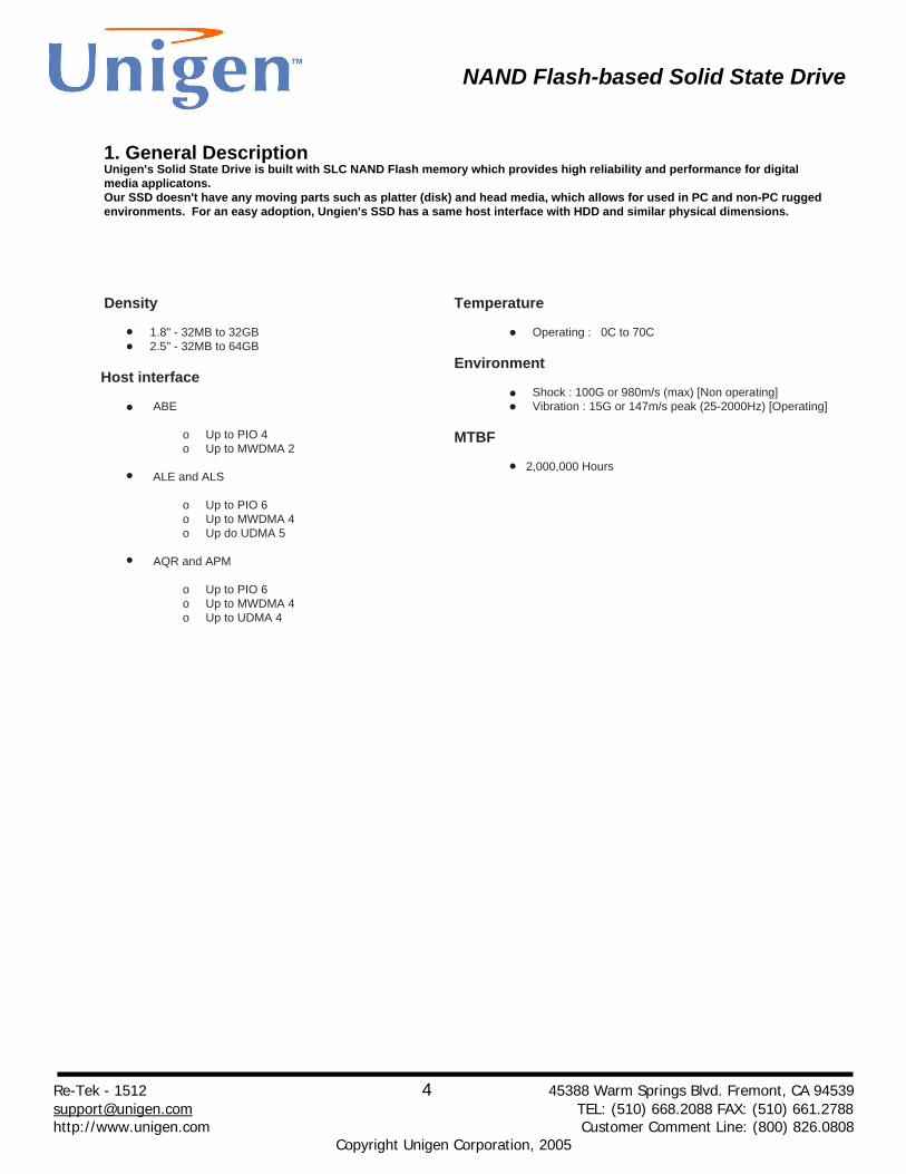
1. General Description Unigen's Solid State Drive is built with SLC NAND Flash memory which provides high reliability and performance for digital media applicatons. Our SSD doesn't have any moving parts such as platter (disk) and head media, which allows for used in PC and non-PC rugged environments. For an easy adoption, Ungien's SSD has a same host interface with HDD and similar physical dimensions.
Density 1.8" - 32MB to 32GB 2.5" - 32MB to 64GB
Host interface ABE o Up to PIO 4 o Up to MWDMA 2 ALE and ALS o Up to PIO 6 o Up to MWDMA 4 o Up do UDMA 5 AQR and APM o Up to PIO 6 o Up to MWDMA 4 o Up to UDMA 4
Temperature Operating : 0C to 70C
Environment Shock : 100G or 980m/s (max) [Non operating] Vibration : 15G or 147m/s peak (25-2000Hz) [Operating]
MTBF 2,000,000 Hours
NAND Flash-based Solid State Drive

NAND Flash-based Solid State Drive
Re-Tek - 1512 5 45388 Warm Springs Blvd. Fremont, CA 94539 [email protected] TEL: (510) 668.2088 FAX: (510) 661.2788 http://www.unigen.com Customer Comment Line: (800) 826.0808
Copyright Unigen Corporation, 2005
2.1 Physical Dimensions
Tolerance size : +/- 3mm2. Physical Specifications
9.50mm
2.35mm4.25mm
70.00mm
50.00mm
100.
00m
m
70.0
0mm
R4
12.00mm
1.8" SSD Drive
70.00mm
60.1
0mm
1.55mm
2.45mm
6.50mm
2.5" SSD Drive
NAND Flash-based Solid State Drive
Re-Tek - 1512 6 45388 Warm Springs Blvd. Fremont, CA 94539 [email protected] TEL: (510) 668.2088 FAX: (510) 661.2788 http://www.unigen.com Customer Comment Line: (800) 826.0808
Copyright Unigen Corporation, 2005
Read / Write Performance(MB/s)
Random Read Sector TBD
Random Write Sector TBD
Sequential Read Sector TBD
Sequential Write Sector TBD
Current Typical(mA)
Active 200
Idle 20
Standby 20
MTBF 1,000,000 Hours
3.1 System Interface and Configuration
3.2 System Performance
3.4 System Reliability
3.3 System Power Consumption
3. Product Specifications
Features Operating
Temperature -0’C ~ 70’C
Humidity 0’C to 55’C / 90~98% RH, 10cycles
Vibration
Shock
3.5 Environmental Specifications
100G or 980m/s, (Max), [Non-Operating]
15G or 147m/s Peak, (25 ~ 2000Hz), [Operating]

NAND Flash-based Solid State Drive
Re-Tesuppohttp://
4. Electrical Specification
4.1 Pin Locations
43 19 C1 A
44 KEY D2 B
The following diagram identifies the Pin Locations of the Unigen SSD Drive.
4.1.1 Pin Assignments
NOTE:Pin 32 was defined as IOCS16 in ATA2, ANSI X3.279-1996Pin 42 is meaningless, because there is no motor in SSD
PIN NAME PIN NAME PIN NAME
1 RESET 16 D14 31 INTRQ
2 GND 17 D0 32 Obsolete(See note)
3 D7 18 D15 33 A1
4 D8 19 GND 34 PDIAG
5 D6 20 KEY 35 A0
6 D9 21 DMARQ 36 A2
7 D5 22 GND 37 CS0
8 D10 23 DIOW 38 CS1
9 D4 24 GND 39 DASP
10 D11 25 DIOR 40 GND
11 D3 26 GND 41 VDD
12 D12 27 IORDY 42 VDD(See note)
13 D2 28 CSEL 43 GND
14 D13 29 DMACK 44 NC
15 D1 30 GND
4.2 Jumper Settings
k - 1512 7 45388 Warm Springs Blvd. Fremont, CA 94539 [email protected] TEL: (510) 668.2088 FAX: (510) 661.2788 www.unigen.com Customer Comment Line: (800) 826.0808
Copyright Unigen Corporation, 2005
Not Need
NAND Flash-based Solid State Drive
Re-Tek - 1512 8 45388 Warm Springs Blvd. Fremont, CA 94539 [email protected] TEL: (510) 668.2088 FAX: (510) 661.2788 http://www.unigen.com Customer Comment Line: (800) 826.0808
Copyright Unigen Corporation, 2005
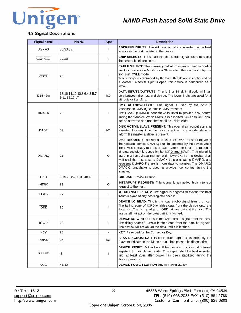
Signal name Pin NO Type Description
A2 - A0 36,33,35 I ADDRESS INPUTS: The Address signal are asserted by the hostto access the task register in the device.
CS0, CS1 37,38 I CHIP SELECTS: These are the chip select signals used to selectthe control block registers.
CSEL 28 I
CABLE SELECT: This internally pulled up signal is used to config-ure this device as a Master or a Slave when the jumper configura-tion is in CSEL mode.When this pin is grounded by the host, this device is configured asa Master. When this pin is open, this device is configured as aslave.
D15 - D0 18,16,14,12,10,8,6,4,3,5,7,9,11,13,15,17 I/O
DATA INPUTS/OUTPUTS: This is 8 or 16 bit bi-directional inter-face between the host and device. The lower 8 bits are used for 8bit register transfers.
DMACK 29 I
DMA ACKNOWLEDGE: This signal is used by the host inresponse to DMARQ to initiate DMA transfers.The DMARQ/DMACK handshake is used to provide flow controlduring the transfer. When DMACK is asserted, CS0 ans CS1 shallnot be asserted and transfers shall be 16bits wide.
DASP 39 I/ODISK ACTIVE/SLAVE PRESENT: This open drain output signal isasserted low any time the drive is active. In a master/slave toinform the master a slave is present.
DMARQ 21 O
DMA REQUEST: This signal is used for DMA transfers betweenthe host and device. DMARQ shall be asserted by the device whenthe device is ready to transfer data to/from the host. The directionof data transfer is controller by IORD and IOWR. This signal isused in a handshake manner with DMACK, i.e the device shallwait until the host asserts DMACK before negating DMARQ, andre-assert DMARQ if there is more data to transfer. The DMARQ/DMACK handshake is used to provide flow control during thetransfer.
GND 2,19,22,24,26,30,40,43 - GROUND: Device Ground.
INTRQ 31 O INTERRUPT REQUEST: This signal is an active high interruptrequest to the host.
IORDY 27 I I/O CHANNEL READY: The signal is negated to extend the hosttransfer cycle of any host register access.
IORD 25 I
DEVICE I/O READ: This is the read strobe signal from the host.The falling edge of IORD enables data from the device onto thedata bus. The rising edge of IORD latches data at the host. Thehost shall not act on the data until it is latched.
IOWR 23 IDEVICE I/O WRITE: This is the write strobe signal from the host.The rising edge of IOWR# latches data from the data bit signals.The device will not act on the data until it is latched.
KEY 20 - KEY: Peserved for the Connector Key.
PDIAG 34 I/O PASS DIAGNOSTIC: This open drain signal is asserted by theSlave to indicate to the Master that it has passed its diagnostics.
RESET
DEVICE RESET: Active Low. When Active, this sets all internalregisters to their default state. This signal shall be held asserteduntil at least 25us after power has been stabilized during thedevice power on.
VCC 41,42 - DEVICE POWER SUPPLY: Device Power 3.3/5V
4.3 Signal Descriptions
1 l

NAND Flash-based Solid State Drive
Re-Tek - 1512 9 45388 Warm Springs Blvd. Fremont, CA 94539 [email protected] TEL: (510) 668.2088 FAX: (510) 661.2788 http://www.unigen.com Customer Comment Line: (800) 826.0808
Copyright Unigen Corporation, 2005
4.4.2 Recommended Operating Conditions
Characteristics Symbol Rating Unit
DC Supply Voltage VDD1.8’’(3.3V) 3.0 to 3.6
V2.5’’(5.0V) 4.5 to 5.5
Input/Output Voltage VIN/VOUT 3.0 to 3.6 V
Operating Temperature TOPR
-40 to 85
-25 to 85 °C
4.4.3 Electrical Characteristics - Normal I/O Vdd = 3.0 to 3.6(V), Ta = 25(°C), Vext = 5V ± 0.25V
NOTE:* Schmitt Trigger test condition : VDD = 3.0 to 3.6(V), Ta = 25(°C)
Characteristic:These DC parameters guarantee the I/O cell characteristic at the static state only, not at the dynamic state.
Characteristics Symbol Test Condition Min Typ Max Unit
Input High Current IIHVIN = VDD
Pull - DownNormalDown
-1010
--
1060
uAuA
Input Low Current IILVIN = VSSPull - Up
NormalUp
-10-60
--
10-10
uAuA
Input High Voltage VIH CMOS 2.0 - - V
Input Low Voltage VIL CMOS - - 0.8 V
Output High Voltage VOH 6mA Buffer, IOH = -6mA 2.4 - - V
Output Low Voltage VOL 6mA Buffer, IOL = 6mA - - 0.4 V
Tri-state Output Leakage Current IOZ VOUT = VDD or VSS -10 - 10 uA
4.4 DC Characteristics
mAIN
Characteristics Symbol Rating Unit
DC Supply Voltage VDD1.8’’(3.3V) 3.0 to 3.6
V2.5’’(5.0V) 4.5 to 5.5
Input/Output Voltage VIN/VOUT 3.0 to 3.6 V
Storage Temperature
DC input Current +/- 200
°C
I
TSTG
4.4.1 Absolute Maximum Ratings
NAND Flash-based Solid State Drive
Re-Tek - 1512 10 45388 Warm Springs Blvd. Fremont, CA 94539 [email protected] TEL: (510) 668.2088 FAX: (510) 661.2788 http://www.unigen.com Customer Comment Line: (800) 826.0808
Copyright Unigen Corporation, 2005
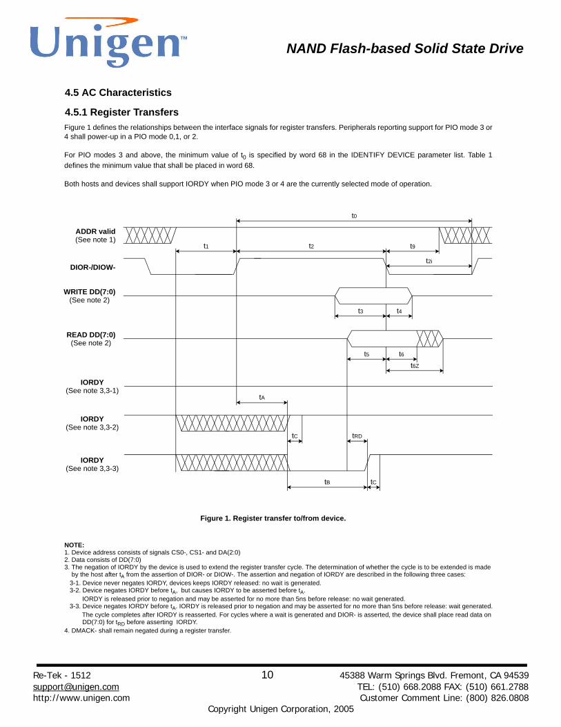
Figure 1 defines the relationships between the interface signals for register transfers. Peripherals reporting support for PIO mode 3 or4 shall power-up in a PIO mode 0,1, or 2.
For PIO modes 3 and above, the minimum value of t0 is specified by word 68 in the IDENTIFY DEVICE parameter list. Table 1defines the minimum value that shall be placed in word 68.
Both hosts and devices shall support IORDY when PIO mode 3 or 4 are the currently selected mode of operation.
DIOR-/DIOW-
WRITE DD(7:0)
READ DD(7:0)
IORDY
t1
ADDR valid
t2(See note 1)
(See note 2)
(See note 2)
(See note 3,3-2)
IORDY(See note 3,3-1)
IORDY(See note 3,3-3)
t9
t0
t3 t4
t5 t6t6Z
tA
tC tRD
tB tC
NOTE:1. Device address consists of signals CS0-, CS1- and DA(2:0)2. Data consists of DD(7:0)3. The negation of IORDY by the device is used to extend the register transfer cycle. The determination of whether the cycle is to be extended is made by the host after tA from the assertion of DIOR- or DIOW-. The assertion and negation of IORDY are described in the following three cases: 3-1. Device never negates IORDY, devices keeps IORDY released: no wait is generated. 3-2. Device negates IORDY before tA, but causes IORDY to be asserted before tA. IORDY is released prior to negation and may be asserted for no more than 5ns before release: no wait generated. 3-3. Device negates IORDY before tA. IORDY is released prior to negation and may be asserted for no more than 5ns before release: wait generated. The cycle completes after IORDY is reasserted. For cycles where a wait is generated and DIOR- is asserted, the device shall place read data on DD(7:0) for tRD before asserting IORDY.4. DMACK- shall remain negated during a register transfer.
Figure 1. Register transfer to/from device.
t2i
4.5.1 Register Transfers
4.5 AC Characteristics
NAND Flash-based Solid State Drive
Re-Tek - 1512 11 45388 Warm Springs Blvd. Fremont, CA 94539 [email protected] TEL: (510) 668.2088 FAX: (510) 661.2788 http://www.unigen.com Customer Comment Line: (800) 826.0808
Copyright Unigen Corporation, 2005
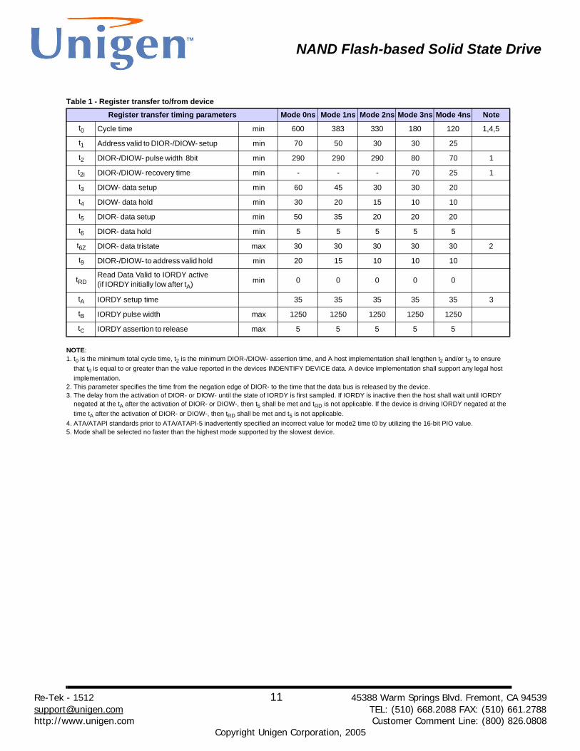
Table 1 - Register transfer to/from device
NOTE:1. t0 is the minimum total cycle time, t2 is the minimum DIOR-/DIOW- assertion time, and A host implementation shall lengthen t2 and/or t2i to ensure that t0 is equal to or greater than the value reported in the devices INDENTIFY DEVICE data. A device implementation shall support any legal host implementation.2. This parameter specifies the time from the negation edge of DIOR- to the time that the data bus is released by the device.3. The delay from the activation of DIOR- or DIOW- until the state of IORDY is first sampled. If IORDY is inactive then the host shall wait until IORDY negated at the tA after the activation of DIOR- or DIOW-, then t5 shall be met and tRD is not applicable. If the device is driving IORDY negated at the time tA after the activation of DIOR- or DIOW-, then tRD shall be met and t5 is not applicable.4. ATA/ATAPI standards prior to ATA/ATAPI-5 inadvertently specified an incorrect value for mode2 time t0 by utilizing the 16-bit PIO value.5. Mode shall be selected no faster than the highest mode supported by the slowest device.
Register transfer timing parameters Mode 0ns Mode 1ns Mode 2ns Mode 3ns Mode 4ns Note
t0 Cycle time min 600 383 330 180 120 1,4,5
t1 Address valid to DIOR-/DIOW- setup min 70 50 30 30 25
t2 DIOR-/DIOW- pulse width 8bit min 290 290 290 80 70 1
t2i DIOR-/DIOW- recovery time min - - - 70 25 1
t3 DIOW- data setup min 60 45 30 30 20
t4 DIOW- data hold min 30 20 15 10 10
t5 DIOR- data setup min 50 35 20 20 20
t6 DIOR- data hold min 5 5 5 5 5
t6Z DIOR- data tristate max 30 30 30 30 30 2
t9 DIOR-/DIOW- to address valid hold min 20 15 10 10 10
tRDRead Data Valid to IORDY active (if IORDY initially low after tA) min 0 0 0 0 0
tA IORDY setup time 35 35 35 35 35 3
tB IORDY pulse width max 1250 1250 1250 1250 1250
tC IORDY assertion to release max 5 5 5 5 5
NAND Flash-based Solid State Drive
Re-Tek - 1512 12 45388 Warm Springs Blvd. Fremont, CA 94539 [email protected] TEL: (510) 668.2088 FAX: (510) 661.2788 http://www.unigen.com Customer Comment Line: (800) 826.0808
Copyright Unigen Corporation, 2005
Figure 2 defines the relationships between the interface signals for PIO data transfers. Peripherals reporting support for PIO mode 3or 4 shall power-up in a PIO mode 0,1, or 2.
For PIO modes 3 and above, the minimum value of t0 is specified by word 68 in the IDENTIFY DEVICE parameter list. Table 2defines the minimum value that shall be placed in word 68.
IORDY shall be supported when PIO mode 3 or 4 are the current mode of operation.
DIOR-/DIOW-
WRITE DD(15:0)
IORDY
t1
ADDR valid
t2(See note 1)
(See note 2)
(See note 3,3-2)
IORDY(See note 3,3-1)
IORDY(See note 3,3-3)
t9
t0
t3 t4
t5 t6t6Z
tA
tC tRD
tB tC
NOTE:1. Device address consists of signals CS0-, CS1- and DA(2:0)2. Data consists of DD(15:0) for all devices except devices implementing the CFA feature set when 8-bit transfers is enabled. In that case, data consists of DD(7:0)3. The negation of IORDY by the device is used to extend the PIO cycle. The determination of whether the cycle is to be extended is made by the host after tA from the assertion of DIOR- or DIOW-. The assertion and negation of IORDY are described in the following three cases: 3-1. Device never negates IORDY, devices keeps IORDY released: no wait is generated. 3-2. Device negates IORDY before tA, but causes IORDY to be asserted before tA. IORDY is released prior to negation and may be asserted for no more than 5ns before release: no wait generated. 3-3. Device negates IORDY before tA. IORDY is released prior to negation and may be asserted for no more than 5ns before release: wait generated. The cycle completes after IORDY is reasserted. For cycles where a wait is generated and DIOR- is asserted, the device shall place read data on DD(7:0) for tRD before asserting IORDY.4. DMACK- shall be negated during a PIO data transfer.
Figure 2. PIO data transfer to/from device.
DD(7:0)
t2i
READ DD(15:0)
(See note 2)DD(7:0)
4.5.2 PIO Data Transfers

NAND Flash-based Solid State Drive
Re-Tek - 1512 13 45388 Warm Springs Blvd. Fremont, CA 94539 [email protected] TEL: (510) 668.2088 FAX: (510) 661.2788 http://www.unigen.com Customer Comment Line: (800) 826.0808
Copyright Unigen Corporation, 2005
Table 2 - PIO data transfer to/from device
NOTE:1. t0 is the minimum total cycle time, t2 is the minimum DIOR-/DIOW- assertion time, and t21 is the minimum DIOR-/DIOW- negation time. A host imple-mentation shall lengthen t2 and/or t2i to ensure that t0 is equal to or greater than the value reported in the devices IDENTIFY DEVICE data. A deviceimplementation shall support any legal host implementation. 2. This parameter specifies the time from the negation edge of DIOR- to the time that the data bus is released by the device.3. The delay from the activation of DIOR- or DIOW- until the state of IORDY is first sampled. If IORDY is inactive then the host shall wait until IORDY isactive before the PIO cycle is completed. If the device is not driving IORDY negated at the tA after the activation of DIOR- or DIOW-, then t5 shall be metand tRD is not applicable. If the device is driving IORDY negated at the time tA after the activation of DIOR- or DIOW-, then tRD shall be met and t5 is notapplicable. 4. Mode may be selected at the highest mode for the device if CS(1:0) and AD(2:0) do not change between read or write cycles or selected at the high-est mode supported by the slowest device if CS(1:0) or AD(2:0) do change between read or write cycles.
PIO timing parameters Mode 0ns Mode 1ns Mode 2ns Mode 3ns Mode 4ns Note
t0 Cycle time min 600 383 240 180 120 1,4
t1 Address valid to DIOR-/DIOW- setup min 70 50 30 30 25
t2 DIOR-/DIOW- min 165 125 100 80 70 1
t2i DIOR-/DIOW- recovery time min - - - 70 25 1
t3 DIOW- data setup min 60 45 30 30 20
t4 DIOW- data hold min 30 20 15 10 10
t5 DIOR- data setup min 50 35 20 20 20
t6 DIOR- data hold min 5 5 5 5 5
t6Z DIOR- data tristate max 30 30 30 30 30 2
t9 DIOR-/DIOW- to address valid hold min 20 15 10 10 10
tRDRead Data Valid to IORDY active (if IORDY initially low after tA )
min 0 0 0 0 0
tA IORDY setup time 35 35 35 35 35 3
tB IORDY pulse width max 1250 1250 1250 1250 1250
tC IORDY assertion to release max 5 5 5 5 5

NAND Flash-based Solid State Drive
Re-Tek - 1512 14 45388 Warm Springs Blvd. Fremont, CA 94539 [email protected] TEL: (510) 668.2088 FAX: (510) 661.2788 http://www.unigen.com Customer Comment Line: (800) 826.0808
Copyright Unigen Corporation, 2005
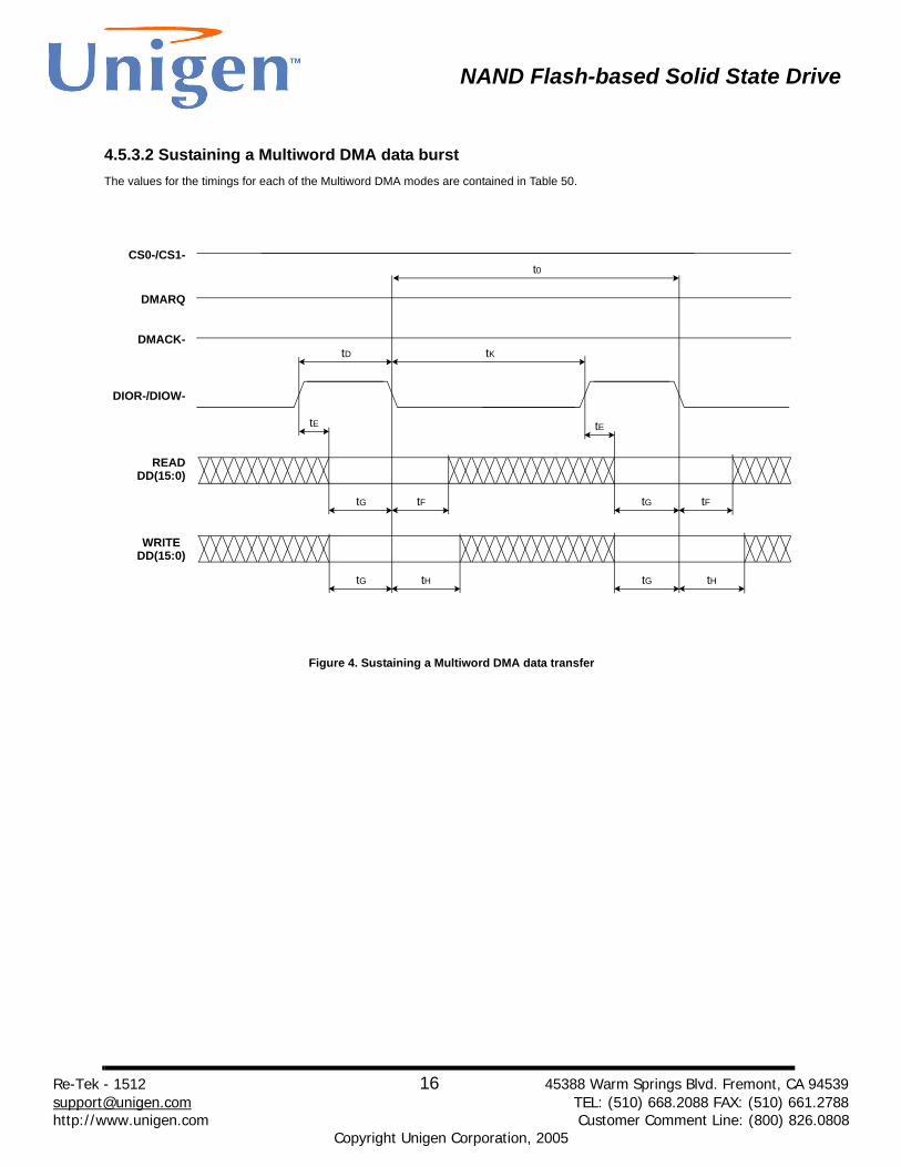
Figure 3 through Figure 6 define the timing associated with Multiword DMA transfers.
For Multiword DMA modes 1 and above, the minimum value of t0 is specified by word 65 in the IDENTIFY DEVICE parameter list.Table 3 defines the minimum value that shall be placed in word 65.
Devices shall power-up with mode 0 as the default Multiword DMA mode.
Table 3 - Multiword DMA data transfer
NOTE:> t0 is the minimum total cycle time, tD is the minimum DIOR-/DIOW- assertion time, and tK (tKR or tKw, as appropriate) is the minimum DIOR-/DIOW-negation time. A host shall lengthen tD and/or tK to ensure that t0 is equal to the value reported in the devices IDENTIFY DEVICE data.
Multiword DMA timing parameters Mode 0ns Mode 1ns Mode 2ns Note
t0 Cycle time min 480 150 120 see note
tD DIOR-/DIOW- asserted pulse width min 215 80 70 see note
tE DIOR- data access max 150 60 50
tF DIOR- data hold min 5 5 5
tG DIOR-/DIOW-data setup min 100 30 20
tH DIOW- data hold min 20 15 10
tI DMACK to DIOR-/DIOW- data setup min 0 0 0
tJ DIOR-/DIOW- to DMACK hold min 20 5 5
tKR DIOR- negated pulse width min 50 50 25 see note
tKW DIOW- negated pulse width min 215 50 25 see note
tLR DIOR- to DMARQ delay max 120 40 35
tLW DIOW- to DMARQ delay max 40 40 35
tM CS(1:0) valid to DIOR-/DIOW- min 50 30 25
tN CS(1:0) hold min 15 10 10
tZ DMACK- to read data released max 20 25 25
4.5.3 Multiword DMA Data Transfers

NAND Flash-based Solid State Drive
Re-Tek - 1512 15 45388 Warm Springs Blvd. Fremont, CA 94539 [email protected] TEL: (510) 668.2088 FAX: (510) 661.2788 http://www.unigen.com Customer Comment Line: (800) 826.0808
Copyright Unigen Corporation, 2005
The values for the timings for each of the Multiword DMA modes are contained in Table 50.
DMARQ
WRITE
CS0-/CS1-
DD(15:0)
READDD(15:0)
tM
Figure 3. Initiating a Multiword DMA data transfer
DIOR-/DIOW-
DMACK-
See note
See note
tE
tD
tG
tG
tF
tH
NOTE: The host shall not assert DMACK- or negate both CS0 and CS1 until the assertion of DMARQ is detected. The maxium time from the assertion ofDMARQ to the assertion of DMACK- or the negation of both CS0 and CS1 is not defined.
4.5.3.1 Initiating a Multiword DMA data burst
NAND Flash-based Solid State Drive
Re-Tek - 1512 16 45388 Warm Springs Blvd. Fremont, CA 94539 [email protected] TEL: (510) 668.2088 FAX: (510) 661.2788 http://www.unigen.com Customer Comment Line: (800) 826.0808
Copyright Unigen Corporation, 2005
The values for the timings for each of the Multiword DMA modes are contained in Table 50.
DMARQ
WRITE
CS0-/CS1-
DD(15:0)
READDD(15:0)
Figure 4. Sustaining a Multiword DMA data transfer
DIOR-/DIOW-
DMACK-tD
t0
tK
tE
tG tF
tE
tG tF
tG tH tG tH
4.5.3.2 Sustaining a Multiword DMA data burst

NAND Flash-based Solid State Drive
Re-Tek - 1512 17 45388 Warm Springs Blvd. Fremont, CA 94539 [email protected] TEL: (510) 668.2088 FAX: (510) 661.2788 http://www.unigen.com Customer Comment Line: (800) 826.0808
Copyright Unigen Corporation, 2005
The values for the timings for each of the Multiword DMA modes are contained in Table 50.
DMARQ
WRITE
CS0-/CS1-
DD(15:0)
READDD(15:0)
Figure 5. Device terminating a Multiword DMA data transfer
DIOR-/DIOW-
DMACK-
t0
tK
tE
tG tF
tG tH
(See note)
tN
tL
tD tJ
tZ
NOTE:To terminate the data burst, the Host shall negate DMARQ within the tL of the assertion of the current DIOR- or DIOW- pulse. The last data word for theburst shall then be transferred by the negation of the current DIOR- or DIOW- pulse. If all data for the command has not been transferred, the Host shallreassert DMARQ again at any later time to resume the DMA operation.
4.5.3.3 Device terminating a Multiword DMA data burst

NAND Flash-based Solid State Drive
Re-Tek - 1512 18 45388 Warm Springs Blvd. Fremont, CA 94539 [email protected] TEL: (510) 668.2088 FAX: (510) 661.2788 http://www.unigen.com Customer Comment Line: (800) 826.0808
Copyright Unigen Corporation, 2005
The values for the timings for each of the Multiword DMA modes are contained in Table 50.
DMARQ
WRITE
CS0-/CS1-
DD(15:0)
READDD(15:0)
Figure 6. Host terminating a Multiword DMA data transfer
DIOR-/DIOW-
DMACK-
t0
tK
tE
tG tF
tG tH
(See note 2)
tN
tD tJ
tZ
NOTE:1. To terminate the transmission of a data burst, the host shall negate DMACK- within the specified time after a DIOR- or DIOW- pulse. No furtherDIOR- or DIOW- pulses shall be asserted for this burst.2. If the device is able to continue the transfer of data, the Host may leave DMARQ asserted and wait for the host to reassert DMACK- or may negateDMARQ at any time after detecting that DMACK- has been negated.
(See note 1)
4.5.3.4 Host terminating a Multiword DMA data burst

NAND Flash-based Solid State Drive
Re-Tek - 1512 19 45388 Warm Springs Blvd. Fremont, CA 94539 [email protected] TEL: (510) 668.2088 FAX: (510) 661.2788 http://www.unigen.com Customer Comment Line: (800) 826.0808
Copyright Unigen Corporation, 2005
Figure 7 through Figure 16 define the timings associated with all phases of Ultra DMA bursts.Table 4 contains the values for the timings for each of the Ultra DMA modes.
Table 4 - Ultra DMA data burst timing requirements
NOTE1. Timing parameters shall be measured at the connector of the sender or receiver to which the parameter applies. For example, the sender shall stop generating STROBE edges tRFS after the negation of DMARDY-. Both STROBE and DMARDY- timing measurements are taken at the connector of the sender.2. All timing measurement switching points(low to high and high to low) shall be taken at 1.5V.3. tUI, tMLI, and tLI indicate sender-to-recipient or recipient-to-sender interlocks, i.e., either sender or recipient is waiting for the other to respond with a signal before proceeding. tUI is an inlimited interlock that has no maximum time value. tMLI is a limited time-out that has a defined minimum. tLI is a lim-ited time-out that has a defined maximum.4. The test load for tDVS and tDVH shall be a lumped capacitor load with no cable or receivers. Timing for tDVS and tDVH shall be met for all capacitive loads from 15 to 40 pf where all signals have the same capacitive load value.5. tZIORDY may be greater than tENV since the device has a pull up on IORDY- giving it a known state when released.
NameMode 0 Mode 1 Mode 2 Mode 3 Mode 4 Comment
(See Notes 1 and 2)min max min max min max min max min maxt2CYCTYP 240 160 120 90 60 Typical sustained average two cycle time
tCYC 112 73 54 39 25 Cycle time allowing for asymmetry and clock varia-tions (from STROBE edge to STROBE edge)
t2CYC 230 154 115 86 57Two cycle time allowing for clock variations (from ris-ing edge to next rising edge or from falling edge tonext falling edge of STROBE)
tDS 15 10 7 7 5 Data setup time at recipient
tDH 5 5 5 5 5 Data hold time at recipient
tDVS 70 48 30 20 6 Data valid setup time at sender (from data valid untilSTROBE edge) (See Note 4)
tDVH 6 6 6 6 6 Data valid hold time at sender (from STROBE edgeuntil data may become invalid) (See Note 4)
tFS 0 230 0 200 0 170 0 130 0 120 First STROBE time (for device to first negateDSTROBE from STOP during a data in burst)
tLI 0 150 0 150 0 150 0 100 0 100 Limited interlock time (See Note 3)
tMLI 20 20 20 20 20 Interlock time with minimum(See Note 3)
tUI 0 0 0 0 0 Unlimited interlock time (See Note 3)
tAZ 10 10 10 10 10 Maximum time allowed for output drivers to release(from asserted or negated)
tZAH 20 20 20 20 20 Minimum delay time required for output
tZAD 0 0 0 0 0 Drivers to assert or negate (from released)
tENV 20 70 20 70 20 70 20 55 20 55Envelope time (from DMACK- to STOP andHDMARDY- during data in burst initiation and fromDMACK to STOP during data out burst initiation)
tSR 50 30 20 NA NASTROBE-to-DMARDY- time (if DMARDY- is negatedbefore this long after STROBE edge, the recipientshall receive no more than one additional data word)
tRFS 75 70 60 60 60 Ready-to-final-STROBE time (no STROBE edgesshall be sent this long after negation of DMARDY-)
tRP 160 125 100 100 100 Minimum time to assert STOP or negate DMARQ
tIORDYZ 20 20 20 20 20 Maximum time before releasing IORDY
tZIORDY 0 0 0 0 0 Minimum time before driving STROBE (See Note 5)
tACK 20 20 20 20 20 Setup and hold times for DMACK- (before assertionor negation)
tSS 50 50 50 50 50 Time from STROBE edge to negation of DMARQ orassertion of STOP (when sender terminates a burst)
4.5.4 Ultra DMA data burst

NAND Flash-based Solid State Drive
Re-Tek - 1512 20 45388 Warm Springs Blvd. Fremont, CA 94539 [email protected] TEL: (510) 668.2088 FAX: (510) 661.2788 http://www.unigen.com Customer Comment Line: (800) 826.0808
Copyright Unigen Corporation, 2005
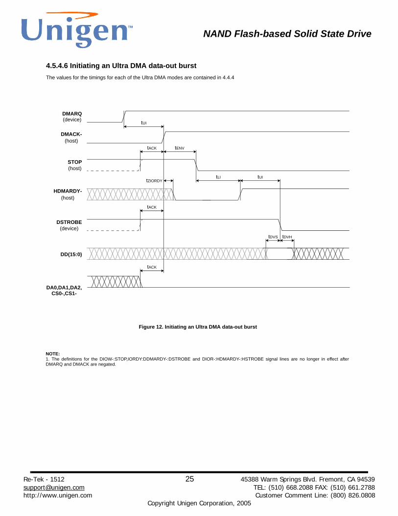
The values for the timings for each of the Ultra DMA modes are contained in 4.4.4
DMACK-
DMARQ
DD(15:0)
DSTROBE(device)
Figure 7. Initiating an Ultra DMA data-in burst
HDMARDY-
STOP
(host)
tUI
(host)
(device)
(host)
DA0,DA1,DA2,CS0-,CS1-
tACK tENV tFS
tZAD
tACK tENV
tZAD
tFS
tZIORDY
tAZ tDVS tDVH
tACK
NOTE:1. The definitions for the DIOW-:STOP, DIOR-:HDMARDY-:HSTROBE and IORDY:DDMARDY-:DSTROBE signal lines are not in effect until DMARQand DMACK are asserted.
4.5.4.1 Initiating an Ultra DMA data-in burst

NAND Flash-based Solid State Drive
Re-Tek - 1512 21 45388 Warm Springs Blvd. Fremont, CA 94539 [email protected] TEL: (510) 668.2088 FAX: (510) 661.2788 http://www.unigen.com Customer Comment Line: (800) 826.0808
Copyright Unigen Corporation, 2005
The values for the timings for each of the Ultra DMA modes are contained in 4.4.4
DD(15:0)
DSTROBE
Figure 8. Sustained Ultra DMA data-in burst
at device
tCYC
at device
tCYC
DSTROBEat host
DD(15:0)at host
t2CYC
t2CYC
tDVH tDVS tDVH tDVS tDVH
tDH tDHtDS tDHtDS
NOTE:1. DD(15:0) and DSTROBE signals are shown at both the host and the device to emphasize that cable setting time as well as cable propagation delay shall not allow the data signals to be considered stable at the host until some time after they are driven by the device.
4.5.4.2 Sustained Ultra DMA data-in burst

NAND Flash-based Solid State Drive
Re-Tek - 1512 22 45388 Warm Springs Blvd. Fremont, CA 94539 [email protected] TEL: (510) 668.2088 FAX: (510) 661.2788 http://www.unigen.com Customer Comment Line: (800) 826.0808
Copyright Unigen Corporation, 2005
The values for the timings for each of the Ultra DMA modes are contained in 4.4.4
DMACK-
DMARQ
DD(15:0)
DSTROBE(device)
Figure 9. Host pausing an Ultra DMA data-in burst
HDMARDY-
STOP
(host)
(host)
(device)
(host)
tSR
tRFS
NOTE:1. The host mat assert STOP to request termination of the ultra DMA burst no sooner than tRP after HDMARDY- is negated.2. If the tSR timing is not satisfied, the host may receive zero, one, or two more data words from the Host.
(device)
tRP
4.5.4.3 Host pausing an Ultra DMA data-in burst

NAND Flash-based Solid State Drive
Re-Tek - 1512 23 45388 Warm Springs Blvd. Fremont, CA 94539 [email protected] TEL: (510) 668.2088 FAX: (510) 661.2788 http://www.unigen.com Customer Comment Line: (800) 826.0808
Copyright Unigen Corporation, 2005
The values for the timings for each of the Ultra DMA modes are contained in 4.4.4
DMACK-
DMARQ
CRC
DSTROBE(device)
HDMARDY-
STOP
(host)
(host)
(device)
(host)
DA0,DA1,DA2,CS0-,CS1-
tSS
tMLI
tACKtLI tLI
tLI
tAZ
tZAH
tACK
tIORDYZ
tACK
tDVH
DD(15:0)
Figure 10. Device terminating an Ultra DMA data-in burst
NOTE:1. The definitions for the DIOW-:STOP, DIOR-:HDMARDY-:HSTROBE and IORDY:DDMARDY-:DSTROBE signal lines are no longer in effect afterDMARQ and DMACK are negated.
4.5.4.4 Device terminating an Ultra DMA data-in burst

NAND Flash-based Solid State Drive
Re-Tek - 1512 24 45388 Warm Springs Blvd. Fremont, CA 94539 [email protected] TEL: (510) 668.2088 FAX: (510) 661.2788 http://www.unigen.com Customer Comment Line: (800) 826.0808
Copyright Unigen Corporation, 2005
The values for the timings for each of the Ultra DMA modes are contained in 4.4.4
DMACK-
DMARQ
DSTROBE(device)
HDMARDY-
STOP
(host)
(host)
(device)
(host)
DA0,DA1,DA2,CS0-,CS1-
tRFS
tMLI
tACKtRP
tZAH
tACK
tIORDYZ
tACK
tDVH
DD(15:0)
Figure 11. Host terminating an Ultra DMA data-in burst
NOTE:1. The definitions for the DIOW-:STOP, DIOR-:HDMARDY-:HSTROBE and IORDY:DDMARDY-:DSTROBE signal lines are no longer in effect afterDMARQ and DMACK are negated.
tLI
tAZ
tLI tMLI
tDVS
4.5.4.5 Host terminating an Ultra DMA data-in burst
CRC
NAND Flash-based Solid State Drive
Re-Tek - 1512 25 45388 Warm Springs Blvd. Fremont, CA 94539 [email protected] TEL: (510) 668.2088 FAX: (510) 661.2788 http://www.unigen.com Customer Comment Line: (800) 826.0808
Copyright Unigen Corporation, 2005
The values for the timings for each of the Ultra DMA modes are contained in 4.4.4
DMACK-
DMARQ
DSTROBE(device)
HDMARDY-
STOP
(host)
(host)
(device)
(host)
DA0,DA1,DA2,CS0-,CS1-
tACK
tDVH
DD(15:0)
Figure 12. Initiating an Ultra DMA data-out burst
NOTE:1. The definitions for the DIOW-:STOP,IORDY:DDMARDY-:DSTROBE and DIOR-:HDMARDY-:HSTROBE signal lines are no longer in effect afterDMARQ and DMACK are negated.
tDVS
tUI
tENV
tZIORDYtLI
tACK
tUI
tACK
4.5.4.6 Initiating an Ultra DMA data-out burst

NAND Flash-based Solid State Drive
Re-Tek - 1512 26 45388 Warm Springs Blvd. Fremont, CA 94539 [email protected] TEL: (510) 668.2088 FAX: (510) 661.2788 http://www.unigen.com Customer Comment Line: (800) 826.0808
Copyright Unigen Corporation, 2005
The values for the timings for each of the Ultra DMA modes are contained in 4.4.4
NOTE:1. DD(15:0) and HSTROBE signals are shown at both the host and the device to emphasize that cable setting time as well as cable propagation delayshall not allow the data signals to be considered stable at the device until some time after they are driven by the host.
DD(15:0)
HSTROBE
Figure 13. Sustained Ultra DMA data-out burst
at host
tCYC
at host
tCYC
HSTROBEat device
DD(15:0)at device
2CYC
t2CYC
tDVH tDVS tDVH tDVS tDVH
tDH tDHtDS tDHtDS
4.5.4.7 Sustained Ultra DMA data-out burst

NAND Flash-based Solid State Drive
Re-Tek - 1512 27 45388 Warm Springs Blvd. Fremont, CA 94539 [email protected] TEL: (510) 668.2088 FAX: (510) 661.2788 http://www.unigen.com Customer Comment Line: (800) 826.0808
Copyright Unigen Corporation, 2005
The values for the timings for each of the Ultra DMA modes are contained in 4.4.4
Figure 14. Device pausing an Ultra DMA data-out burst
NOTE:1. The device may negate DMARQ to request termination of the Ultra DMA burst no sooner that tRP after DDMARDY- is negated.2. If the tSR timing is not satisfied, the device may receive zero,one,or two more data words from the host.
STOP
DMACK-
DD(15:0)
HSTROBE(host)
DDMARDY-
DMARQ
(host)
(device)
(host)
(device)
tSR
tRFS
(host)
tRP
4.5.4.8 Device pausing an Ultra DMA data-out burst
NAND Flash-based Solid State Drive
Re-Tek - 1512 28 45388 Warm Springs Blvd. Fremont, CA 94539 [email protected] TEL: (510) 668.2088 FAX: (510) 661.2788 http://www.unigen.com Customer Comment Line: (800) 826.0808
Copyright Unigen Corporation, 2005
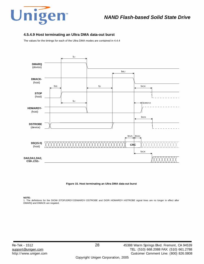
The values for the timings for each of the Ultra DMA modes are contained in 4.4.4
DMACK-
DMARQ
CRC
DSTROBE(device)
HDMARDY-
STOP
(host)
(host)
(device)
(host)
DA0,DA1,DA2,CS0-,CS1-
tSS
tMLI
tACKtLI
tLI
tACK
tIORDYZ
tACK
tDVH
DD(15:0)
Figure 15. Host terminating an Ultra DMA data-out burst
NOTE:1. The definitions for the DIOW-:STOP,IORDY:DDMARDY-:DSTROBE and DIOR-:HDMARDY-:HSTROBE signal lines are no longer in effect afterDMARQ and DMACK are negated.
tLI
tDVS
(host)
4.5.4.9 Host terminating an Ultra DMA data-out burst

NAND Flash-based Solid State Drive
Re-Tek - 1512 29 45388 Warm Springs Blvd. Fremont, CA 94539 [email protected] TEL: (510) 668.2088 FAX: (510) 661.2788 http://www.unigen.com Customer Comment Line: (800) 826.0808
Copyright Unigen Corporation, 2005
The values for the timings for each of the Ultra DMA modes are contained in 4.4.4
DMACK-
DMARQ
CRC
HSTROBE(host)
DDMARDY-
STOP
(host)
(host)
(device)
(device)
DA0,DA1,DA2,CS0-,CS1-
tRFS
tMLI
tRP
tACK
tDVH
Figure 16. Device terminating an Ultra DMA data-out burst
NOTE:1. The definitions for the DIOW-:STOP,IORDY:DDMARDY-:DSTROBE and DIOR-:HDMARDY-:HSTROBE signal lines are no longer in effect afterDMARQ and DMACK are negated.
tLI
tLI tMLI
tDVS
DD(15:0)(host)
tACK
tIORDYZ
tACK
4.5.4.10 Device terminating an Ultra DMA data-out burst
NAND Flash-based Solid State Drive
Re-Tesuppohttp:/
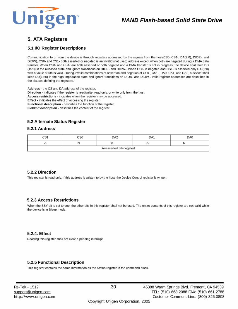
5.1 I/O Register Descriptions
Communication to or from the device is through registers addressed by the signals from the host(CS0-,CS1-, DA(2:0), DIOR-, andDIOW), CS0- and CS1- both asserted or negated is an invalid (not used) address except when both are negated during a DMA datatransfer. When CS0- and CS1- are both asserted or both negated and a DMA transfer is not in progress, the device shall hold DD(15:0) in the released state and ignore transitions on DIOR- and DIOW-. When CS0- is negated and CS1- is asserted only DA (2:0)with a value of 6th is valid. During invalid combinations of assertion and negation of CS0-, CS1-, DA0, DA1, and DA2, a device shallkeep DD(15:0) in the high impedance state and ignore transitions on DIOR- and DIOW-. Valid register addresses are described inthe clauses defining the registers.
Address - the CS and DA address of the register.Direction - indicates if the register is read/write, read only, or write only from the host.Access restrictions - indicates when the register may be accessed.Effect - indicates the effect of accessing the register.Functional description - describes the function of the register.Field/bit description - describes the content of the register.
5. ATA Registers
5.2 Alternate Status Register
5.2.1 AddressCS1 CS0 DA2 DA1 DA0
A N A A N
A=asserted, N=negated
5.2.2 DirectionThis register is read only. If this address is written to by the host, the Device Control register is written.
5.2.3 Access Restrictions
When the BSY bit is set to one, the other bits in this register shall not be used. The entire contents of this register are not valid whilethe device is in Sleep mode.5.2.4. Effect
k - 1512 30 45388 Warm Springs Blvd. Fremont, CA 94539 [email protected] TEL: (510) 668.2088 FAX: (510) 661.2788 /www.unigen.com Customer Comment Line: (800) 826.0808
Copyright Unigen Corporation, 2005
5.2.5 Functional Description
Reading this register shall not clear a pending interrupt.
This register contains the same information as the Status register in the command block.

NAND Flash-based Solid State Drive
Re-Tek - 1512 31 45388 Warm Springs Blvd. Fremont, CA 94539 [email protected] TEL: (510) 668.2088 FAX: (510) 661.2788 http://www.unigen.com Customer Comment Line: (800) 826.0808
Copyright Unigen Corporation, 2005
5.3 Command Register5.3.1 Address
CS1 CS0 DA2 DA1 DA0
N A A A N
A=asserted, N=negated
This register is write only. If this address is read by the host, the Status register is read.
5.3.3 Access RestrictionsFor all commands, this register shall only be written when BSY and DRQ are both cleared to zero and DMACK- is not asserted. Ifwritten when BSY or DRQ is set to one, the results of writing the Command register are indeterminate.
5.3.4 Effect
5.3.5 Functional description
5.3.6 Field/bit description7 6 5 4 3 2 1 0
Command Code
Command prcessing begins when this register is writte. The content of the Command Blcok registers become parameters of the command when this register is written. Writing this register clears any pending interrupt condition.
This register contains the command code being sent to the device. Command execution begins immediately after this register is writ-ten.
5.3.2 Direction

NAND Flash-based Solid State Drive
Re-Tek - 1512 32 45388 Warm Springs Blvd. Fremont, CA 94539 [email protected] TEL: (510) 668.2088 FAX: (510) 661.2788 http://www.unigen.com Customer Comment Line: (800) 826.0808
Copyright Unigen Corporation, 2005
5.4.4 EffectThe content of this register becomes a command parameter when the Comand register is written.
5.4.5 Functional descriptionThe content of this register is command dependent
5.4.3 Access RestrictionsThis register shall be written only when both BSY and DRQ are cleared to zero and DMACK- is noet asserted.The contents of this register are valid only when BSY is cleared to zero. If this register is written when BSY or DRQ is set to one, theresult is indeterminate. The contents of this register are not valid while a device is in the Sleep mode.
5.4.2 DirectionThis register is read/write.
5.4 Cylinder High Register5.4.1 Address
CS1 CS0 DA2 DA1 DA0
N A A N A
A=asserted, N=negated

NAND Flash-based Solid State Drive
Re-Tesuppohttp://
k - 1512 33 45388 Warm Springs Blvd. Fremont, CA 94539 [email protected] TEL: (510) 668.2088 FAX: (510) 661.2788 www.unigen.com Customer Comment Line: (800) 826.0808
Copyright Unigen Corporation, 2005
5.5.1 AddressCS1 CS0 DA2 DA1 DA0
N A A N N
A=asserted, N=negated
5.5.2 Direction
5.5.4 Effect
5.5.3 Access Restrictions
This register is read/write.
This register shall be written only when both BSY and DRQ are cleared to zero and DMACK- is not asserted.The contents of this register are valid only when BSY is cleared to zero. If this register is written when BSY or DRQ is set to one, theresult is indeterminate. The contents of this register are not valid while a device is in the Sleep mode.
The content of this register becomes a command parameter when the Command register is written.
5.6 Data Port
CS1 CS0 DA2 DA1 DA0
N N X X X
A=asserted, N=negated, X=don’t care
5.5.5 Functional descriptionThe content of this register is command dependent
5.6.1 AddressWhen DMACK- is asserted, CS0- and CS1- shall be negated and transfers shall be 16-bits wide.
5.6.2 DirectionThis register is read/write.
5.5 Cylinder Low Register
NAND Flash-based Solid State Drive
Re-Tek - 1512 34 45388 Warm Springs Blvd. Fremont, CA 94539 [email protected] TEL: (510) 668.2088 FAX: (510) 661.2788 http://www.unigen.com Customer Comment Line: (800) 826.0808
Copyright Unigen Corporation, 2005
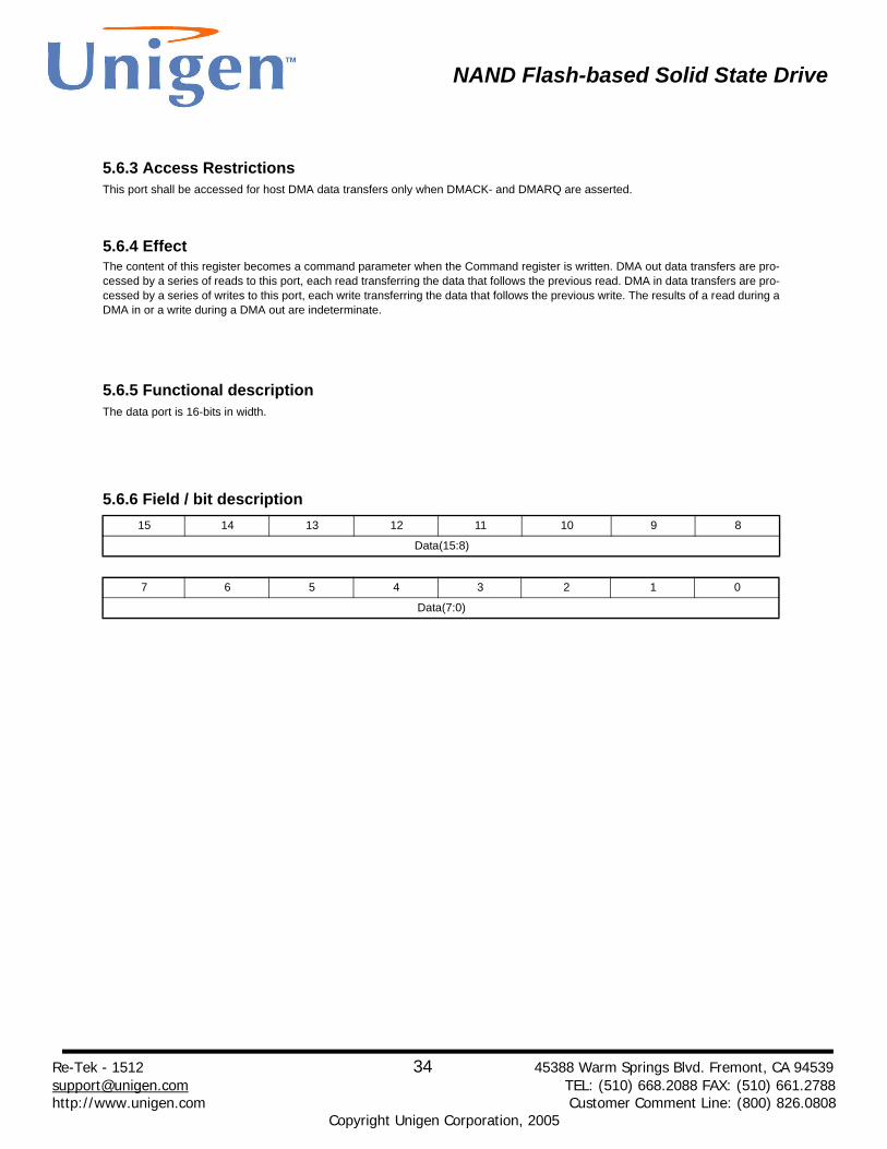
5.6.3 Access RestrictionsThis port shall be accessed for host DMA data transfers only when DMACK- and DMARQ are asserted.
5.6.4 EffectThe content of this register becomes a command parameter when the Command register is written. DMA out data transfers are pro-cessed by a series of reads to this port, each read transferring the data that follows the previous read. DMA in data transfers are pro-cessed by a series of writes to this port, each write transferring the data that follows the previous write. The results of a read during aDMA in or a write during a DMA out are indeterminate.
The data port is 16-bits in width.
5.6.6 Field / bit description15 14 13 12 11 10 9 8
Data(15:8)
7 6 5 4 3 2 1 0
Data(7:0)
5.6.5 Functional description

NAND Flash-based Solid State Drive
Re-Tesuppohttp://
5.7 Data Register5.7.1 Address
CS1 CS0 DA2 DA1 DA0
N A N N N
A=asserted, N=negated
5.7.2 DirectionThis register is read/write.
5.7.3 Access Restrictions
This register shall be accessed for host PIO data transfer only when DRQ is set to on and DMACK- is not asserted.The contents of this register are not valid while a device is in the Sleep mode.5.7.4 Effect
k - 1512 35 45388 Warm Springs Blvd. Fremont, CA 94539 [email protected] TEL: (510) 668.2088 FAX: (510) 661.2788 www.unigen.com Customer Comment Line: (800) 826.0808
Copyright Unigen Corporation, 2005
PIO out data transfers are processed by a series of reads to this register, each read transferring the data that follows the previousread. PIO in data transfers are processed by a series of writes to this register, each write transferring the data that follows the previ-ous write. The results of a read during a PIO in or a write during a PIO out are indeterminate.
5.7.5 Functional descriptionThe data port is 16-bits in width. When a CFA device is in 8-bit PIO data transfer mode this register is 8-bits wide using only DD7 toDD0.
5.7.6 Field / bit description15 14 13 12 11 10 9 8
Data(15:8)
7 6 5 4 3 2 1 0
Data(7:0)

NAND Flash-based Solid State Drive
Re-Tek - 1512 36 45388 Warm Springs Blvd. Fremont, CA 94539 [email protected] TEL: (510) 668.2088 FAX: (510) 661.2788 http://www.unigen.com Customer Comment Line: (800) 826.0808
Copyright Unigen Corporation, 2005
5.8.1 Address
CS1 CS0 DA2 DA1 DA0
A N A A N
A=asserted, N=negated
5.8.6 Field / bit description
Bits 7 through 3 are reserved. SRST is the host software reset bit. nIEN is the enable bit for the device Assertion of INTRQ to the host. When the nIEN bit is cleared to zero, and the device is
selected, INTRQ shall be enabled through a tri-state buffer and shall be asserted or negated by the device as appropriate. When thenIEN bit is set to one, or the device is not selected, the INTRQ signal shall be in a high impedance state.
Bit 0 shall be cleared to zero.
7 6 5 4 3 2 1 0
r r r r r SRST nIEN 0
5.8.2 DirectionThis register is write only. If this address is read by the host, the Alternate Status register is read.
5.8.3 Access RestrictionsThis register shall only be written when DMACK- is not asserted.
The content of this register shall take effect when written.
5.8.5 Functional descriptionThis register allows a host to software reset attached devices and to enable or disable the assertion of the INTRQ signal by aselected device. When the Device Control Register is written, both devices respond to the write regardless of which device isselected. When the SRST bit is set to one, both devices shall perform the software reset protocol.The device shall respond to the SRST bit when in the SLEEP mode.
5.8 Device Control Register
5.8.4 Effect
NAND Flash-based Solid State Drive
Re-Tek - 1512 37 45388 Warm Springs Blvd. Fremont, CA 94539 [email protected] TEL: (510) 668.2088 FAX: (510) 661.2788 http://www.unigen.com Customer Comment Line: (800) 826.0808
Copyright Unigen Corporation, 2005
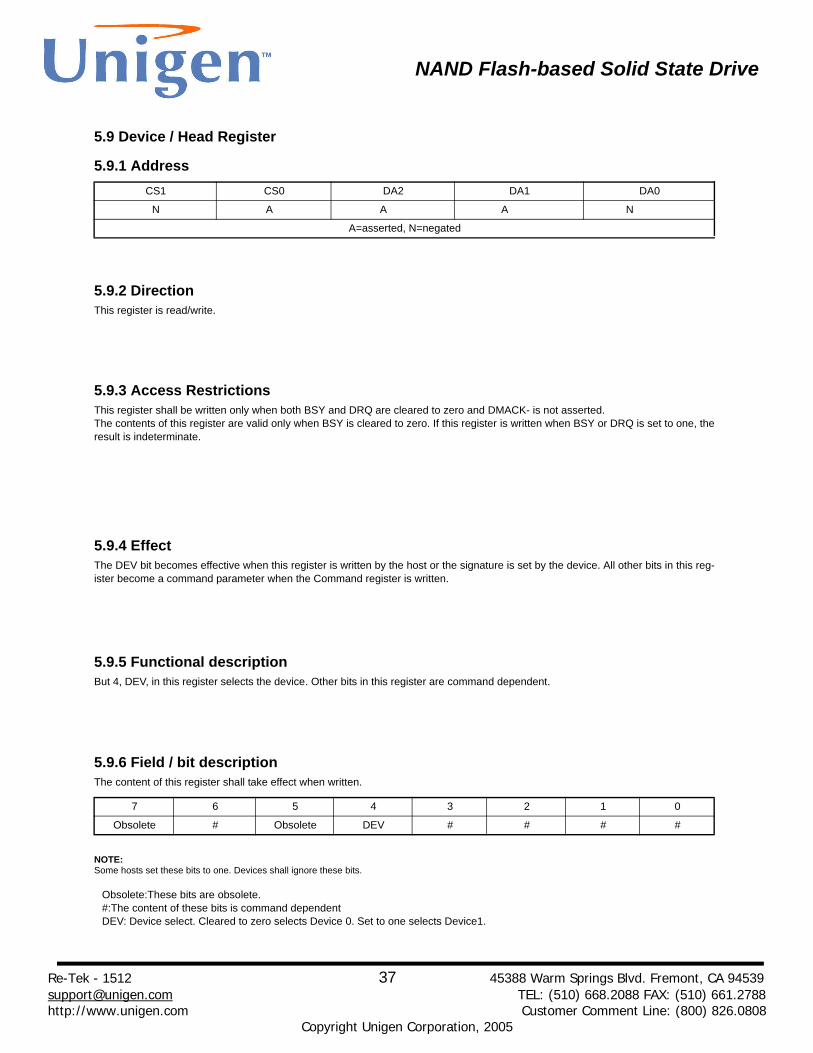
5.9.1 AddressCS1 CS0 DA2 DA1 DA0
N A A A N
A=asserted, N=negated
NOTE:Some hosts set these bits to one. Devices shall ignore these bits.
Obsolete:These bits are obsolete. #:The content of these bits is command dependent DEV: Device select. Cleared to zero selects Device 0. Set to one selects Device1.
7 6 5 4 3 2 1 0
Obsolete # Obsolete DEV # # # #
5.9.2 DirectionThis register is read/write.
5.9.3 Access RestrictionsThis register shall be written only when both BSY and DRQ are cleared to zero and DMACK- is not asserted. The contents of this register are valid only when BSY is cleared to zero. If this register is written when BSY or DRQ is set to one, theresult is indeterminate.
5.9.4 EffectThe DEV bit becomes effective when this register is written by the host or the signature is set by the device. All other bits in this reg-ister become a command parameter when the Command register is written.
5.9.5 Functional descriptionBut 4, DEV, in this register selects the device. Other bits in this register are command dependent.
5.9.6 Field / bit descriptionThe content of this register shall take effect when written.
5.9 Device / Head Register
NAND Flash-based Solid State Drive
Re-Tek - 1512 38 45388 Warm Springs Blvd. Fremont, CA 94539 [email protected] TEL: (510) 668.2088 FAX: (510) 661.2788 http://www.unigen.com Customer Comment Line: (800) 826.0808
Copyright Unigen Corporation, 2005
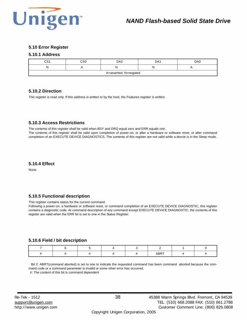
5.10.1 AddressCS1 CS0 DA2 DA1 DA0
N A N N A
A=asserted, N=negated
5.10.6 Field / bit description
Bit 2: ABRT(command aborted) is set to one to indicate the requested command has been command aborted because the com-mand code or a command parameter is invalid or some other error has occurred.#: The content of this bit is command dependent
7 6 5 4 3 2 1 0
# # # # # ABRT # #
5.10.2 DirectionThis register is read only. If this address is written to by the host, the Features register is written.
5.10.3 Access RestrictionsThe contents of this register shall be valid when BSY and DRQ equal zero and ERR equals one.The contents of this register shall be valid upon completion of power-on, or after a hardware or software reset, or after commandcompletion of an EXECUTE DEVICE DIAGNOSTICS. The contents of this register are not valid while a devcie is in the Sleep mode.
5.10.4 EffectNone.
5.10.5 Functional descriptionThis register contains status for the current command.Following a power-on, a hardware or software reset, or command completion of an EXECUTE DEVICE DIAGNOSTIC, this registercontains a diagnostic code. At command description of any command except EXECUTE DEVICE DIAGNOSTIC, the contents of thisregister are valid when the ERR bit is set to one in the Status Register.
5.10 Error Register
NAND Flash-based Solid State Drive
Re-Tek - 1512 39 45388 Warm Springs Blvd. Fremont, CA 94539 [email protected] TEL: (510) 668.2088 FAX: (510) 661.2788 http://www.unigen.com Customer Comment Line: (800) 826.0808
Copyright Unigen Corporation, 2005
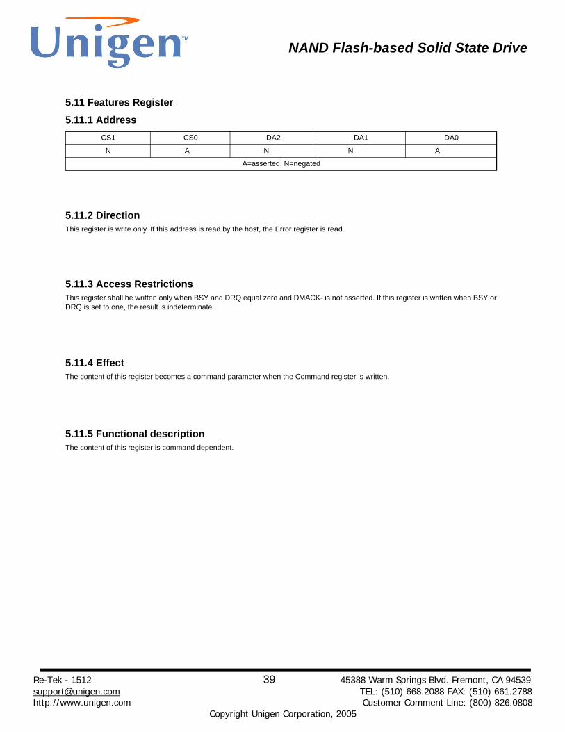
5.11.1 AddressCS1 CS0 DA2 DA1 DA0
N A N N A
A=asserted, N=negated
5.11.2 DirectionThis register is write only. If this address is read by the host, the Error register is read.
5.11.3 Access RestrictionsThis register shall be written only when BSY and DRQ equal zero and DMACK- is not asserted. If this register is written when BSY orDRQ is set to one, the result is indeterminate.
5.11.4 EffectThe content of this register becomes a command parameter when the Command register is written.
5.11.5 Functional descriptionThe content of this register is command dependent.
5.11 Features Register

NAND Flash-based Solid State Drive
Re-Tek - 1512 40 45388 Warm Springs Blvd. Fremont, CA 94539 [email protected] TEL: (510) 668.2088 FAX: (510) 661.2788 http://www.unigen.com Customer Comment Line: (800) 826.0808
Copyright Unigen Corporation, 2005
5.12 Sector Count Register5.12.1 Address
CS1 CS0 DA2 DA1 DA0
N A N A N
A=asserted, N=negated
5.12.2 DirectionThis register is read/write.
5.12.3 Access RestrictionsThis register shall be written only when BSY and DRQ equal zero and DMACK- is not asserted. The contents of this register are validonly when both BSY and DRQ are zero. If this register is written when BSY or DRQ is set to one, the result is indeterminate. The con-tents of the this register are not valid while a device is in the Sleep mode.
5.12.4 EffectThe content of this register becomes a command parameter when the Command register is written.
5.12.5 Functional descriptionThe content of this register is command dependent.

NAND Flash-based Solid State Drive
Re-Tek - 1512 41 45388 Warm Springs Blvd. Fremont, CA 94539 [email protected] TEL: (510) 668.2088 FAX: (510) 661.2788 http://www.unigen.com Customer Comment Line: (800) 826.0808
Copyright Unigen Corporation, 2005
5.13.1 AddressCS1 CS0 DA2 DA1 DA0
N A N A A
A=asserted, N=negated
5.13.2 DirectionThis register is read/write.
5.13.3 Access RestrictionsThis register shall be written only when BSY and DRQ equal zero and DMACK- is not asserted. The contents of this register are validonly when both BSY and DRQ are zero. If this register is written when BSY or DRQ is set to one, the result is indeterminate. The con-tents of the this register are not valid while a device is in the Sleep mode.
5.13.4 EffectThe content of this register becomes a command parameter when the Command register is written.
5.13.5 Functional descriptionThe content of this register is command dependent.
5.13 Sector Number Register

NAND Flash-based Solid State Drive
Re-Tek - 1512 42 45388 Warm Springs Blvd. Fremont, CA 94539 [email protected] TEL: (510) 668.2088 FAX: (510) 661.2788 http://www.unigen.com Customer Comment Line: (800) 826.0808
Copyright Unigen Corporation, 2005
5.14 Status Register5.14.1 Address
CS1 CS0 DA2 DA1 DA0
N A A A A
A=asserted, N=negated
5.14.2 DirectionThis register is read only. If this address is written to by the host, the Command register is written.
5.14.3 Access RestrictionsThe contents of this register, except for BSY, shall be ignored when BSY is set to one. BSY is valid at all times. The contents of thisregister are not valid while a device is in the Sleep mode.
5.14.4 EffectReading this register when an interrupt is pending causes the interrupt pending to be cleared. The host should not read the StatusRegister when an interrupt is expected as this may clear the interrupt pending before the INTRQ can be recognized by the host.
5.14.6 Field / bit description7 6 5 4 3 2 1 0
BSY DRDY # # DRQ Obsolete Obsolete ERR
The register contains the device status. The contents of this register are updated to reflect the current state of the device and theprogress of any command being executed by the device.
5.14.5 Functional description
NAND Flash-based Solid State Drive
Re-Tek - 1512 43 45388 Warm Springs Blvd. Fremont, CA 94539 [email protected] TEL: (510) 668.2088 FAX: (510) 661.2788 http://www.unigen.com Customer Comment Line: (800) 826.0808
Copyright Unigen Corporation, 2005
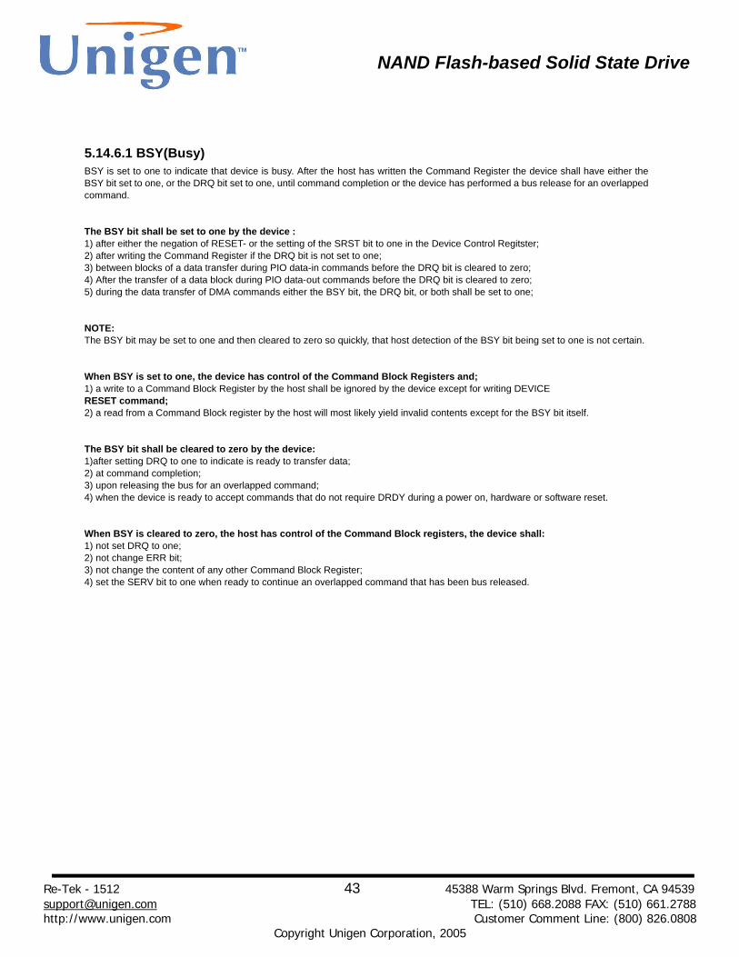
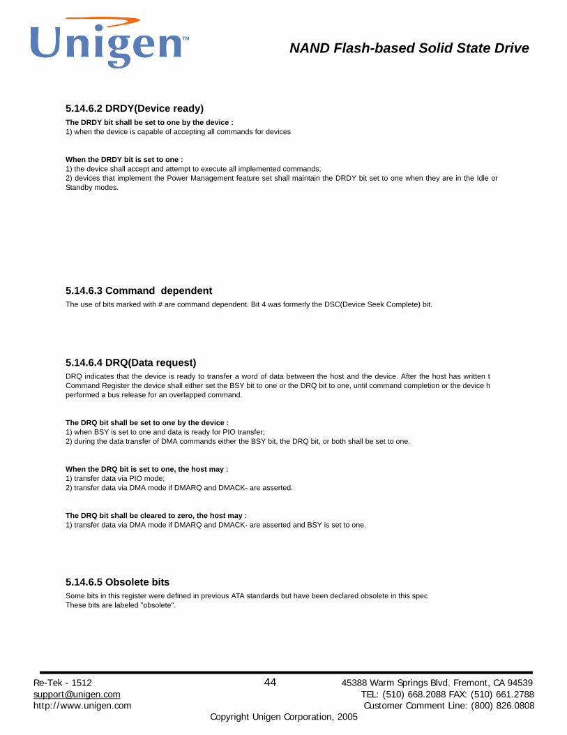
5.14.6.1 BSY(Busy)BSY is set to one to indicate that device is busy. After the host has written the Command Register the device shall have either theBSY bit set to one, or the DRQ bit set to one, until command completion or the device has performed a bus release for an overlappedcommand.
The BSY bit shall be set to one by the device : 1) after either the negation of RESET- or the setting of the SRST bit to one in the Device Control Regitster;2) after writing the Command Register if the DRQ bit is not set to one;3) between blocks of a data transfer during PIO data-in commands before the DRQ bit is cleared to zero;4) After the transfer of a data block during PIO data-out commands before the DRQ bit is cleared to zero;5) during the data transfer of DMA commands either the BSY bit, the DRQ bit, or both shall be set to one;
NOTE:The BSY bit may be set to one and then cleared to zero so quickly, that host detection of the BSY bit being set to one is not certain.
When BSY is set to one, the device has control of the Command Block Registers and;1) a write to a Command Block Register by the host shall be ignored by the device except for writing DEVICE RESET command;2) a read from a Command Block register by the host will most likely yield invalid contents except for the BSY bit itself.
The BSY bit shall be cleared to zero by the device:1)after setting DRQ to one to indicate is ready to transfer data;2) at command completion;3) upon releasing the bus for an overlapped command;4) when the device is ready to accept commands that do not require DRDY during a power on, hardware or software reset.
When BSY is cleared to zero, the host has control of the Command Block registers, the device shall:1) not set DRQ to one;2) not change ERR bit;3) not change the content of any other Command Block Register;4) set the SERV bit to one when ready to continue an overlapped command that has been bus released.
NAND Flash-based Solid State Drive
Re-Tek - 1512 44 45388 Warm Springs Blvd. Fremont, CA 94539 [email protected] TEL: (510) 668.2088 FAX: (510) 661.2788 http://www.unigen.com Customer Comment Line: (800) 826.0808
Copyright Unigen Corporation, 2005
The DRDY bit shall be set to one by the device : 1) when the device is capable of accepting all commands for devices
When the DRDY bit is set to one :1) the device shall accept and attempt to execute all implemented commands;2) devices that implement the Power Management feature set shall maintain the DRDY bit set to one when they are in the Idle orStandby modes.
5.14.6.3 Command dependentThe use of bits marked with # are command dependent. Bit 4 was formerly the DSC(Device Seek Complete) bit.
5.14.6.4 DRQ(Data request)DRQ indicates that the device is ready to transfer a word of data between the host and the device. After the host has written tCommand Register the device shall either set the BSY bit to one or the DRQ bit to one, until command completion or the device hperformed a bus release for an overlapped command.
The DRQ bit shall be set to one by the device : 1) when BSY is set to one and data is ready for PIO transfer;2) during the data transfer of DMA commands either the BSY bit, the DRQ bit, or both shall be set to one.
When the DRQ bit is set to one, the host may :1) transfer data via PIO mode;2) transfer data via DMA mode if DMARQ and DMACK- are asserted.
The DRQ bit shall be cleared to zero, the host may :1) transfer data via DMA mode if DMARQ and DMACK- are asserted and BSY is set to one.
5.14.6.5 Obsolete bitsSome bits in this register were defined in previous ATA standards but have been declared obsolete in this specThese bits are labeled "obsolete".
5.14.6.2 DRDY(Device ready)

NAND Flash-based Solid State Drive
Re-Tek - 1512 45 45388 Warm Springs Blvd. Fremont, CA 94539 [email protected] TEL: (510) 668.2088 FAX: (510) 661.2788 http://www.unigen.com Customer Comment Line: (800) 826.0808
Copyright Unigen Corporation, 2005
ERR indicates that an error occurred during execution of the previous command.
The ERR bit shall be set to one by the device :1) when BSY or DRQ is set to one and an error occurs in the executing command.
When the ERR bit is set to one :1) the bits in the Error register shall be valid;2) the device shall not change the contents of the following registers until a new command has been accepted, the SRST bit is set toone or RESET- is asserted :
Error Register Cylinder High/Low Register Sector Count Register Sector Number Register Device / Head Register
The ERR bit shall be cleared to zero by the device :1) when a new command is written to the Command Register;2) when the SRST bit is set to one;3) when the RESET- signal is asserted.
When the ERR bit is cleared to zero at the end of a command:1) the content of the Error Register shall be ignored by the host.
5.14.6.6 ERR(Error)

NAND Flash-based Solid State Drive
Re-Tesuppohttp://
6. Command Descriptions
k - 1512 46 45388 Warm Springs Blvd. Fremont, CA 94539 [email protected] TEL: (510) 668.2088 FAX: (510) 661.2788 www.unigen.com Customer Comment Line: (800) 826.0808
Copyright Unigen Corporation, 2005
*1 : Refer to 6.3.1*2 : Refer to 6.5.1*3 : Refer to 6.6.1
Command Name Command Code Command Name Command Code
RECALIBRATE 10h IDLE E3h
READ SECTOR(S) 20h READ BUFFER E4h
WRITE SECTOR(S) 30h CHECK POWER MODE E5h
READ VERIFY SECTOR(S) 40h SLEEP E6h
SEEK 70h FLUSH CACHE E7h
EXECUTE DEVICE DIAGNOSTIC 90h WRITE BUFFER E8h
INITIALIZE DEVICE PARAMETERS 91h IDENTIFY DEVICE ECh
SMART*1 B0h SET FEATURES*2 EFh
READ MULTIPLE C4h SECURITY SET PASSWORD F1h
WRITE MULTIPLE C5h SECURITY UNLOCK F2h
SET MULTIPLE MODE C6h SECURITY ERASE PREPARE F3h
READ DMA C8h SECURITY ERASE UNIT F4h
WRITE DMA CAh SECURITY FREEZE LOCK F5h
STANDBY IMMEDIATE E0h SECURITY DISABLE PASSWORD F6h
IDLE IMMEDIATE E1h READ NATIVE MAX ADDRESS F8h
STANBY E2h SET MAX*3 F9h
6.1 Supporting ATA Command Set
NAND Flash-based Solid State Drive
Re-Tesuppohttp://
6.2 SECURITY FEATURE Set
k - 1512 47 45388 Warm Springs Blvd. Fremont, CA 94539 [email protected] TEL: (510) 668.2088 FAX: (510) 661.2788 www.unigen.com Customer Comment Line: (800) 826.0808
Copyright Unigen Corporation, 2005
The Security mode features allow the host to implement a securtity password system to prevent unauthorized access to the diskdrive.
The NSSD is shipped with master password set to 20h value(ASCII blanks) and the lock function disabled.The system manufacturer/dealer may set a new master password by using the SECURITY SET PASSWORD command, withoutenableing the lock function.
When a user password is set, the drive automatically enters lock mode by the next powered-on
In locked mode, the NSSD rejects media access commands until a SECURITY UNLOCK command is successfully completed.
If the user password is lost and High level security is set, the drive does not allow the user to access any data.However, the drive can be unlocked using the master password.
If the user password is lost and Maxium security level is set, it is impossible to access data. However, the drive can be unlocked using the ERASE UNIT command with the master password. The drive will erase all user dataand unlock the drive.
The execution time of SECURITY ERASE UNIT command is shown below. - 64GB NSSD : 60 seconds - 48GB NSSD : 45 seconds - 32GB NSSD : 30 seconds - 16GB NSSD : 15 seconds - 8GB NSSD : 8 seconds
6.2.1 SECURITY mode default setting
6.2.2 Initial setting of the user password
6.2.3 SECURITY mode operation from power-on
6.2.4 Password lost

NAND Flash-based Solid State Drive
Re-Tek - 1512 48 45388 Warm Springs Blvd. Fremont, CA 94539 [email protected] TEL: (510) 668.2088 FAX: (510) 661.2788 http://www.unigen.com Customer Comment Line: (800) 826.0808
Copyright Unigen Corporation, 2005
SMART
READ DATA D0h READ LOG D5h
READ ATTRIBUTE THRESHOLDS D1h ENABLE OPERATIONS D8h
ENABLE/DISABLE AUTOSAVE D2h DISABLE OPERATIONS D9h
SAVE ATTRIBUTE VALUES D3h RETURN STATUS DAh
EXECUTE OFF-LINE IMMIDIATE D4h CHANGE THRESHOLD SECTOR SIZE E0h
Byte F/V Descriptions
0~1 X Revision code
2~3 X Valid Information Count
4~7 V Total number of sectors for replacement
8~11 V Number of sectors actually replaced
12~15 X Number of sectors initially mapped out
16~19 V Threshold sector size [default value :19000h(50MB)]
19~361 X Vendor specific
362 V Off-line data collection status
363 X Self-test execution status byte
364~365 V Total time in seconds to complete off-line data collection activity
366 X Vendor specific
367 F Off-line data collection capability
368-369 F SMART capability
370 FError logging capability 7-1 Reserved 0 1=Device error logging supported
371 X Vendor specific
372 F Short self-test routine recommended polling time(in minutes)
373 F Extended self-test routine recommended polling time(in minutes)
374-385 R Reserved
386-510 X Vendor specific
511 V Data structure checksum
Key : F=the content of the byte is fixed and does not change. V=the content of the byte is variable and may change depending on the state of the device or the commands executed by the device. X=the content of the byte is vendor specific and may be fixed or variable. R=the content of the byte is reserved and shall be zero.
6.3 SMART FEATURE Set
6.3.2 SMART Data Structure(READ DATA(D0h))
6.3.1 Sub Command Set

NAND Flash-based Solid State Drive
Re-Tek - 1512 49 45388 Warm Springs Blvd. Fremont, CA 94539 [email protected] TEL: (510) 668.2088 FAX: (510) 661.2788 http://www.unigen.com Customer Comment Line: (800) 826.0808
Copyright Unigen Corporation, 2005
Threshold Sector Size is an predefined value that makes the waring message if the number of reserved sector size is below thisvalue. The status can be read from Cylinder Register by READ DATA(D0h) command. Deafult value of the Cylinder Register has C24Fh, but if the number of reserved sector size is below the Treshold Sector Size, theCylinder Register has 2CF4h.In order to change the Threshold Sector Size, should be set the changed value in Sector Count Register with CHANGE THRESH-OLD SECTOR SIZE (E0h) command.
Sector Count Register value (unit : MB, Range : 0~199)
In SLEEP command, NSSD takes 1ms to get into SLEEP state.During this period, all the command operation is prohibitted.The status Register value is D0h after getting into SLEEP state.
SLEEP Command issue SLEEP Command clear
Wait 1 msec
NSSD is set to SLEEP state
BSY
6.3.3 Threshold Sector Size
6.4 BSY Status in SLEEP Command
*
NAND Flash-based Solid State Drive
Re-Tek - 1512 50 45388 Warm Springs Blvd. Fremont, CA 94539 [email protected] TEL: (510) 668.2088 FAX: (510) 661.2788 http://www.unigen.com Customer Comment Line: (800) 826.0808
Copyright Unigen Corporation, 2005
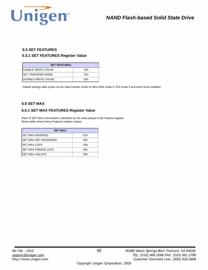
Default settings after power on are Data transfer mode of Ultra DMA mode 4, PIO mode 4 and write cache enabled.
SET FEATURES
ENABLE WRITE CACHE 02h
SET TRANSFER MODE 03h
DISABLE WRITE CACHE 82h
6.5 SET FEATURES6.5.1 SET FEATURES Register Value
Each of SET MAX commands is identified by the value placed in the Feature register. Below table shows these Features register values.
SET MAX
SET MAX ADDRESS 01h
SET MAX SET PASSWORD 02h
SET MAX LOCK 03h
SET MAX FREEZE LOCK 04h
SET MAX UNLOCK 05h
6.6 SET MAX
6.6.1 SET MAX FEATURES Register Value

NAND Flash-based Solid State Drive
Re-Tek - 1512 51 45388 Warm Springs Blvd. Fremont, CA 94539 [email protected] TEL: (510) 668.2088 FAX: (510) 661.2788 http://www.unigen.com Customer Comment Line: (800) 826.0808
Copyright Unigen Corporation, 2005
6.7 Hardware Reset State Diagram
DHR0:RESET-PDIAG-=X, DASP-=X, BSY=1
RESET-negated(t=0)
DHR0:DHR1
RESET-asserted
xx:DHR0
t=1ms
D0HR1:Sample_DASP-PDIAG-=R, DASP-=R, BSY-=1
Sample DASP-D0HR1:D0HR1
DASP-assertedD0HR1:D0HR2
D0HR1:D0HR3Clear bit 7
D0HR2:Sample_PDIAG-PDIAG-=R, DASP-=R, BSY=1
Resemble PDIAG-
D0HR2:D0HR2PDIAG-asserted
t=31ms
D0HR2b:D0HR3Set bit 7
DHR1:Release_busPDIAG-=R, DASP-=X, BSY=1
Bus release & Device 1
DHR1:D1HR0
Bus release & Device 0
DHR1:D0HR1
D1HR0:Set_DASP-PDIAG-=R, DASP-=R, BSY=1
DASP-assertedD1HR0:D1HR1
D1HR1:Set_statusPDIAG-=R, DASP-=A, BSY=1
Status set, passed diagnosticD1HR1:DI2BSY=0, PDIAG-=A
Device_idle_NS
Status set, failed diagnosticD1HR1:DI2BSY=0, PDIAG-=N Device_idle_NS
D0HR3:Set_statusPDIAG-=R, DASP-=R, BSY=1
Status setD0HR3:DI1BSY=0
Device_idle_S
D0HR0:DASP-_waitPDIAG-=R, DASP-=R, BSY=1
D0HR0:D0HR1
t=500ms
D0HR2a:D0HR3Clear bit 7
BSY DRQ REL SERV C/D I/O INTRQ DMARQ PDIAG- DASP-V 0 0 0 0 0 R R V V

NAND Flash-based Solid State Drive
Re-Tek - 1512 52 45388 Warm Springs Blvd. Fremont, CA 94539 [email protected] TEL: (510) 668.2088 FAX: (510) 661.2788 http://www.unigen.com Customer Comment Line: (800) 826.0808
Copyright Unigen Corporation, 2005
6.8 Software Reset State Diagram
D0SR0:SRSTPDIAG-=R, BSY=1
SRST cleared to zero & no Device 1 (t=0)SRST set to one
xx:D0SR0
t=1ms
D0SR2:D0SR2
Resemble PDIAG-
D0SR1:D0SR2
t=6s
D0SR3:Set_statusPDIAG-=R, BSY=1
D0SR1:PDIAG-_waitPDIAG-=R, BSY=1
BSY DRQ REL SERV C/D I/O INTRQ DMARQ PDIAG- DASP-V 0 0 0 0 0 R R V R
D0SR0:D0SR3Clear bit 7
SRST cleared to zero & no Device 1 (t=0)D0SR0:D0SR1
D0SR2:Sample_PDIAG-PDIAG-=R, BSY=1
PDIAG-asserted
D0SR2a:D0SR3Clear bit 7
D0SR2b:D0SR3Set bit 7
Status Set
D0SR3:DI1BSY=0 Device_idle_S
Device0 : software reset state diagram
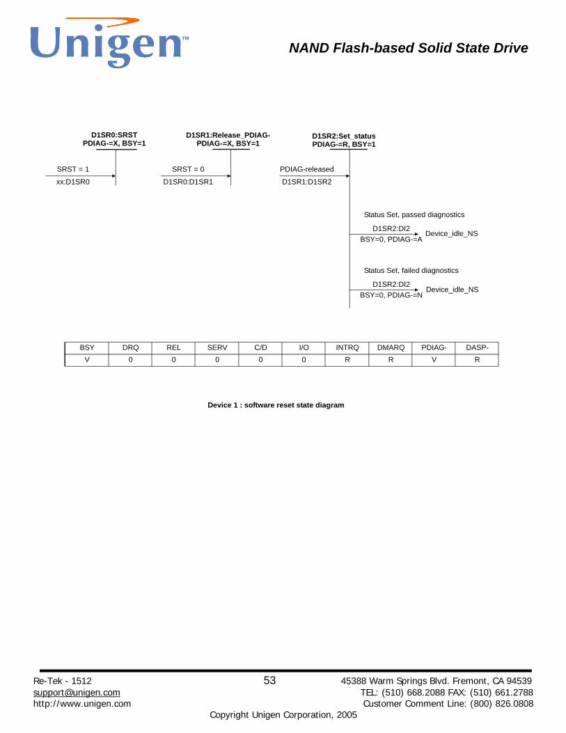
NAND Flash-based Solid State Drive
Re-Tek - 1512 53 45388 Warm Springs Blvd. Fremont, CA 94539 [email protected] TEL: (510) 668.2088 FAX: (510) 661.2788 http://www.unigen.com Customer Comment Line: (800) 826.0808
Copyright Unigen Corporation, 2005
SRST = 1
xx:D1SR0
D1SR1:Release_PDIAG-PDIAG-=X, BSY=1
BSY DRQ REL SERV C/D I/O INTRQ DMARQ PDIAG- DASP-V 0 0 0 0 0 R R V R
Status Set, passed diagnostics
D1SR2:DI2BSY=0, PDIAG-=A
Device_idle_NS
D1SR0:SRSTPDIAG-=X, BSY=1
D1SR2:Set_statusPDIAG-=R, BSY=1
SRST = 0
D1SR0:D1SR1
PDIAG-released
D1SR1:D1SR2
Status Set, failed diagnostics
D1SR2:DI2BSY=0, PDIAG-=N
Device_idle_NS
Device 1 : software reset state diagram

NAND Flash-based Solid State Drive
Re-Tesuppohttp://
7. P
Un
T
BB
A
ABALALAQAP
k - 1512 54 45388 Warm Springs Blvd. Fremont, CA 94539 [email protected] TEL: (510) 668.2088 FAX: (510) 661.2788 www.unigen.com Customer Comment Line: (800) 826.0808
Copyright Unigen Corporation, 2005
art Number and Ordering Information
UG BXX XXX XXXX XX
igen
ype of Memory Card
80 = 2.5" IDE91 = 1.8" IDE
ssembly Code
E = 2.5 IDE with F2E = 1.8 IDE with SMI223S = 2.5 IDE with SMI223R = 1.8 IDE with F2M = 2.5 IDE with F3
Density 0032 = 32MB 0064 = 64MB 0128 = 128MB 0256 = 256MB 0512 = 512MB 1000 = 1.0GB 2000 = 2.0GB 4000 = 4.0GB 8000 = 8.0GB16H0 = 16.0GB32H0 = 32.0GB64H0 = 64.0GB
AQR & APM Firmware S1 = IDE U1 = IDE w/DMA
ABE Firmware C3 = w/o DMA D3 = w/DMA
ALE / ALS Firmware
P1 = IDE Q1 = IDE w/DMA