unisonic technologies co., ltd sop-8
TRANSCRIPT

UNISONIC TECHNOLOGIES CO., LTD
UC3853A Advance LINEAR INTEGRATED CIRCUIT
www.unisonic.com.tw 1 of 14
Copyright © 2020 Unisonic Technologies Co., Ltd QW-R103-167.b
CURRENT MODE PWM
CONTROLLER FOR FORWARD
AND FLYBACK APPLICATIONS
DESCRIPTION
The UTC UC3853A is a high performance current mode PWM
controller ideally suited for low standby power. Low VDD startup
current make the power reliable on startup design and a large
value resistor could be used to minimize the standby power. At no
load condition, the IC operates in power-saving mode for lower
standby power, decreasing frequency for Higher conversion
efficiency at light load condition. It contains protection with
automatic recovery including OLP, OCP, VCC OVP, BNO and OTP.
To protect the power MOSFET, Gate-drive output is fixed up to 15V
max.
Excellent EMI performance is achieved with UTC proprietary
frequency hopping technique (ZL201020615247.1) together with
soft driver control. The controller offers everything needed to build
cost−effective and reliable ac−dc switching supplies dedicated to
ATX power supplies. Finally a SOP-8 package saves PCB space
and represents a solution of choice in cost sensitive project.
SOP-8
FEATURES
* Peak Current Mode Control
* Adjustable Switching Frequency
* Adjustable Soft−start Timer
* Adjustable Internal Ramp Compensation
* Jittering Frequency ±6% of the Switching Frequency
* Power-saving mode for high standby efficiency
* Auto−recovery Primary OCP with 10ms Fixed Delay
* Auto−recovery Brown−Out Detection
* Delayed Operation Upon Start−up via an Internal Fixed
Timer
* UC384X−like UVLO Thresholds
* VCC from 9V to 28V with Auto−recovery UVLO
* Internal 350ns Leading Edge Blanking
* Gate output voltage clamped at 15V
* UC3853A: Maximum 47% Duty Cycle
ORDERING INFORMATION
Ordering Number Package Packing
Lead Free Halogen Free
UC3853AL-S08-R UC3853AG-S08-R SOP-8 Tape Reel
UC3853AG-S08-R
(1)Packing Type
(2)Package Type
(1) R: Tape Reel
(2) S08: SOP-8
(3) G: Halogen Free and Lead Free, L: Lead Free(3)Green Package
(4)Duty Cycle (4) A: 47%

UC3853A Advance LINEAR INTEGRATED CIRCUIT
UNISONIC TECHNOLOGIES CO., LTD 2 of 14
www.unisonic.com.tw QW-R103-067.b
MARKING
UTC
UC3853
1 2 3 4
5678
Date Code
Lot Code
L: Lead Free
G: Halogen FreeDuty Cycle
A: 47%
PIN CONFIGURATION
1
2
3
4
8
7
6
5
FB
BO
CS
RT
SS
VCC
DRV
GND
PIN DESCRIPTION
PIN NO. PIN NAME DESCRIPTION
1 FB Feedback input pin. The PWM duty cycle is determined by voltage level into this pin
and SENSE pin input
2 BO Line input voltage brown out protection
3 CS Current sense input pin. Connected to MOSFET current sensing resistor node
4 RT A resistor connected to ground defined the switching frequency
5 GND Ground
6 DRV This pin connects to the MOSFET gate
7 VCC Power supply
8 SS A capacitor connected to ground defined the soft start time

UC3853A Advance LINEAR INTEGRATED CIRCUIT
UNISONIC TECHNOLOGIES CO., LTD 3 of 14
www.unisonic.com.tw QW-R103-067.b
BLOCK DIAGRAM
Q
Fault
Timer
(15mS)Reset
S Q
QR
3.5V
0V
Buffered
Ramp
UVLO
UVLO Reset
VCC
Management
32V
15V
CLK
S Q
QR
UC3853A: Maximum 47% Duty Cycle
SS_en VDD
GND
ISSDelay
120msUVLO
SS
UVLO Reset
1V
2R
R
Buffered
Ramp
LEB
Rramp
CS
BO
IBO
VBO
RT
VCC
DrvDriver
VDD
FB
VFB_IN
por
OSC
Ton
Ton
por CLK
OCP
OCP
OCP
VSS
VSS
por
Over Load&Open Loop Protection (OLP)
SS_en
SS_en

UC3853A Advance LINEAR INTEGRATED CIRCUIT
UNISONIC TECHNOLOGIES CO., LTD 4 of 14
www.unisonic.com.tw QW-R103-067.b
ABSOLUTE MAXIMUM RATING
PARAMETER SYMBOL RATINGS UNIT
Power Supply Voltage, VCC Pin, OVP Voltage VCC 29 V
Power Supply Voltage, VCC Pin, Continuous Voltage VCC 28 V
Maximum Current Injected Into Pin 7 IVCC 20 mA
Maximum Voltage On Low Power Pins (Except pin 6, 7) -0.3 ~ 10 V
Maximum Junction Temperature TJ +150 °C
Storage Temperature Range TOPR -60 ~ +150 °C
Note: Absolute maximum ratings are those values beyond which the device could be permanently damaged.
Absolute maximum ratings are stress ratings only and functional device operation is not implied.
THERMAL DATA
PARAMETER SYMBOL RATINGS UNIT
Typical Thermal Resistance θJA 169 °C/W
ELECTRICAL DATA
(VCC=15V, RT=43kΩ, CDRV=1nF. For typical values TJ=25°C, for min/max values TJ=–25°C~+125°C, unless
otherwise noted)
PARAMETER SYMBOL TEST CONDITIONS MIN TYP MAX UNIT
SUPPLY SECTION AND VCC MANAGEMENT
Startup Threshold At Which Driving
Pulses Are Authorized VCC_ON VCC increasing 9.4 10 10.6 V
Minimum Operating Voltage At
Which Driving Pulses Are Stopped VCC_OFF VCC decreasing 8.3 9 9.6 V
Start−up Current, Controller
Disabled ISTR VCC<VCC(on)&VCC increasing from zero 5 20 μA
Internal IC Consumption, Controller
Switching ICC FB=3.5V, RT=43kΩ 0.5 1.1 2 mA
OVP Threshold VCC_OVP FB=3.5V,RT=43KΩ 26.5 28.5 30.5 V
CURRENT COMPARATOR
Current Sense Voltage Threshold VILIM 0.89 0.96 1.04 V
Leading Edge Blanking Duration tLEB (Note 1) 350 ns
Internal Ramp Compensation
Voltage Level VRamp @ 25°C (Note 2) 3.15 3.5 3.85 V
Internal Ramp Compensation
Resistance To CS Pin RRamp @ 25°C (Note 2) 26.5 kΩ
INTERNAL OSCILLATOR
Oscillator Frequency fOSC RT=43kΩ & DRV pin=47kΩ 90 100 110 kHz
Frequency Modulation In
Percentage Of fOSC fJitter (Note 1) ±6 %
Maximum Duty Cycle DC_Max. UC3853A 42 46 50 %
FEEDBACK SECTION
Internal Voltage Division From FB
To CS Setpoint FBDIV (Note 1) 3
Internal Pull−Up Resistor RPull−up (Note 1) 3.5 kΩ
FB Pin Maximum Current IFB FB pin=GND 1 mA
Open Loop Feedback Voltage VFBOL FB pin=OPEN 5.4 V
Burst-Mode Enter FB Voltage VFB-IN 0.63 V
Burst-Mode Quit FB Voltage VFB-OUT 0.66 V
UC3853A Advance LINEAR INTEGRATED CIRCUIT
UNISONIC TECHNOLOGIES CO., LTD 5 of 14
www.unisonic.com.tw QW-R103-067.b
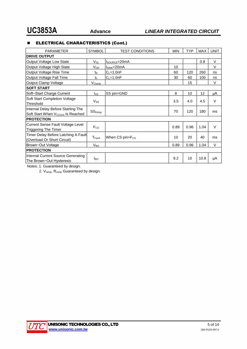
ELECTRICAL CHARACTERISTICS (Cont.)
PARAMETER SYMBOL TEST CONDITIONS MIN TYP MAX UNIT
DRIVE OUTPUT
Output Voltage Low State VOL ISOURCE=20mA 0.8 V
Output Voltage High State VOH ISINK=20mA 10 V
Output Voltage Rise Time tR CL=1.0nF 60 120 260 ns
Output Voltage Fall Time tF CL=1.0nF 30 60 100 ns
Output Clamp Voltage VClamp 15 V
SOFT START
Soft−Start Charge Current ISS SS pin=GND 8 10 12 μA
Soft Start Completion Voltage
Threshold VSS 3.5 4.0 4.5 V
Internal Delay Before Starting The
Soft Start When VCC(on) Is Reached SSDelay 70 120 180 ms
PROTECTION
Current Sense Fault Voltage Level
Triggering The Timer FCS 0.89 0.96 1.04 V
Timer Delay Before Latching A Fault
(Overload Or Short Circuit) TFault When CS pin>FCS 10 20 40 ms
Brown−Out Voltage VBO 0.89 0.96 1.04 V
PROTECTION
Internal Current Source Generating
The Brown−Out Hysteresis IBO 9.2 10 10.8 μA
Notes: 1. Guaranteed by design.
2. Vramp, Rramp Guaranteed by design.

UC3853A Advance LINEAR INTEGRATED CIRCUIT
UNISONIC TECHNOLOGIES CO., LTD 6 of 14
www.unisonic.com.tw QW-R103-067.b
APPLICATION INFORMATION
Introduction
The UTC UC3853A hosts a high−performance current−mode controller specifically developed to drive power
supplies designed for the ATX and the adapter market:
Current Mode operation
Implementing peak current−mode control topology, the circuit offers UC384X−like features to build rugged power
supplies.
Adjustable switching frequency
A resistor to ground precisely sets the switching frequency.
Internal frequency jittering
Frequency jittering softens the EMI signature by spreading out peak energy within a band ±6% from the center
frequency.
Wide VCC excursion
The controller allows operation up to 28V continuously and IC will be shutdown when VCC transient voltage up to
29V.
Gate drive clamping
The controller includes a low−loss clamping voltage which prevents the gate from going beyond 15V typical.
Low startup−current
The start−up current is guaranteed to be less than 5μA maximum, helping the designer to reach a low standby
power level.
Open Loop&Over Load&Short−circuit protection
When VCS exceeds 0.96V , the controller detects a fault and starts an internal digital timer. On the condition that
the digital timer elapses 20mS, the controller will shutdown. Reset occurs when: a) a BO reset is sensed, b) VCC is
cycled down to VCC(min) level.
Adjustable soft−start
The soft−start is activated upon a start−up sequence after a minimum internal time delay of 120m (SSdelay). But
also when the brown−out pin is reset without in that case timer delay. The soft start pin I grounded until the internal
delay is ended.
Shutdown
if an external transistor brings the BO pin down, the controller is shut down, but all internal biasing circuits are alive.
When the pin is released, a new soft−start sequence takes place.
Brown−Out protection
When BO pin voltage is below the VBO threshold, the circuit stays off and does not switch. When BO pin voltage
comes back within safe limits, the pulses are re−started via a start−up sequence including soft−start. The hysteresis
I implemented via a current source connected to the BO pin, which sinks a current (IBO) from the pin to the ground. it
can easily be used for hysteresis purposes.
Internal ramp compensation
A resistor connected from the CS pin to the sense resistor allows the designer to inject ramp compensation inside
his design.

UC3853A Advance LINEAR INTEGRATED CIRCUIT
UNISONIC TECHNOLOGIES CO., LTD 7 of 14
www.unisonic.com.tw QW-R103-067.b
APPLICATION INFORMATION (Cont.)
Burst mode
If the output loads disappear, the FB is allowed to decreases down to VFB_IN, zero duty cycle is imposed. This
mode helps to ensure no−load outputs conditions as requested by recently updated ATX specifications. Bust mode
easily obtains 100mW standby power. The following figure illustrates the different mode of operation versus the FB
pin level.
FB level
VFBOL
VFB_out
Normal Operation:DCmin<DC<DCmaxA/B
Operation @ Ton_min :DC=DCmin
Burst mode:DC=0%Time
Figure 1. Mode Of Operation Versus The FB Pin Level
VFB_IN
Startup Sequence
The startup sequence is activated when Vcc pin reaches VCC(on) level,and the internal delay timer (SSdelay) runs.
Only when the internal delay end,the soft start can be allowed if the BO pin level is above VBO level. The soft start is
allowed if the BO pin threshold is reached,and the voltage on the SS pin is rising from the ground. An external
capacitor connected on SS pin is used to defined SS time. The voltage variation of the SS pin divided by 4 gives the
peak current variation on the CS pin.
The following figures illustrate the different startup cases.
VCC pin
VCC(on)
BO pin
VBO
SS pin
DRV pin
Time
Time
Time
Time
Time
Time
Time
VCC pin
VCC(on)
BO pin
VBO
SS pin
DRV pin
Internal
delay
120mS
Soft start
(A) (B)
Time
Soft start
No
pulse
Figure 2. Startup Sequence (A) & (B)
Internal
delay
120mS

UC3853A Advance LINEAR INTEGRATED CIRCUIT
UNISONIC TECHNOLOGIES CO., LTD 8 of 14
www.unisonic.com.tw QW-R103-067.b
APPLICATION INFORMATION (Cont.)
For the (A), when the VCC pin reaches the VCC(on) level, the internal timer starts. As the BO pin level is above the
VBO threshold at the end of the internal delay, a soft start sequence is started. For the (B), at the end of the internal
delay, the BO pin level is below the VBO threshold thus the soft start sequence can not start. A new soft start
sequence will start only when the BO pin reaches the VBO threshold.
When the BO pin is grounded, the controller is shut down and the SS pin is internally grounded. If the BO pin is
released, a new soft start sequence happens after its level reaches the VBO level.
VCC pin
VCC(on)
BO pin
VBO
SS pin
DRV pin
Time
Time
Time
VCC pin
VCC(on)
BO pin
VBO
SS pin
DRV pin
Time
Time
Time
Time(C)
Time(D)
Figure 3. Brown Out Protection
Soft Start
As illustrated by the following figure, the rising voltage on the SS pin voltage divided by 4 controls the peak current
sensed on the CS pin. Thus as soon as the CS pin voltage becomes higher than the SS pin voltage divided by 4 the
driver is off cycle by cycle.
Rcomp CS
LEB
RCS
SS_en
Vdd
Iss
SS
CSS
1/4
por
UVLODelay
120ms
S Q
QR
CLK DRV
Figure 5. Soft Start
SS_en

UC3853A Advance LINEAR INTEGRATED CIRCUIT
UNISONIC TECHNOLOGIES CO., LTD 9 of 14
www.unisonic.com.tw QW-R103-067.b
APPLICATION INFORMATION (Cont.)
The following figure illustrates a soft start sequence.
Figure 6. Soft Start Example
Brown−Out Protection
The controller protects converter against low input voltage conditions by monitoring the Voltage on BO pin. When
the BO pin voltage falls below the VBO, the controllers stops pulsing until the input level goes back to normal and
resumes the operation via a new soft start sequence.The hysteresis is implemented by using the internal current
connected between the BO pin and the ground when the BO pin is below the VBO.
IBO
Vbulk
RBO1BO
RBO2shutdown VBO
UVLO resetpor
Q
QS
R
Figure 7. BO Pin Setup
The following equations show how to calculate the resistors for BO pin. First of all, select the bulk voltage value at
which the controller must start switching (Vbulkon) and the bulk voltage for shutdown (Vbulkoff) the controller. Where:
Vbulkon=370V, Vbulkoff=350V, VBO=0.96V, IBO=9.8μA. When BO pin voltage is below VBO, the internal current source
(IBO) is activated. The following equation can be written:
ONbulkV =RBO1 (BOI +
2BOR
VBO + BOV (eq. 1)

UC3853A Advance LINEAR INTEGRATED CIRCUIT
UNISONIC TECHNOLOGIES CO., LTD 10 of 14
www.unisonic.com.tw QW-R103-067.b
APPLICATION INFORMATION (Cont.)
When BO pin voltage is higher than VBO, the internal current source is now disabled. The following equation can
be written:
BOV =
12
2bulk
BOBO
BOoff
RR
RV
(eq. 2)
From Equation 2 it can be extracted the RBO1:
RBO1= (BO
BObulkoff
V
V-V)
2BOR (eq. 3)
Equation 3 is substituted in Equation 1 and solved for RBO2, yields:
RBO2= (BO
BO
I
V1-
V-V
V-V
BObulkoff
BObulkon ) (eq. 4)
RBO1 can be also written independently of RBO2 by substituting Equation 4 into Equation 3 as follow:
RBO1=BO
bulkoffbulkon
I
V-V (eq. 5)
From Equation 4 and Equation 5, the resistor divider value can be calculated:
RBO2= 8.9
96.01-
96.0-503
96.0-703 )=5613Ω, RBO1=μ8.9
350-703 =2.04MΩ
Short Circuit or Open Loop&Over Load Protection
A short circuit or an open loop&overload situation is detected when the CS pin voltage reaching 0.96V. If the
condition continued for 15ms, the fault is latched and the controller permanently stops the pulses on the driver pin.
If the fault is latched the controller can be reset if a BO reset is sensed or if VCC is cycled down to VCC(off).
Figure 8. Short Circuit Detection Example
Shut Down
There is one possibility to shut down the controller; this possibility consists at grounding the BO pin as illustrated in
Figure 7.
UC3853A Advance LINEAR INTEGRATED CIRCUIT
UNISONIC TECHNOLOGIES CO., LTD 11 of 14
www.unisonic.com.tw QW-R103-067.b
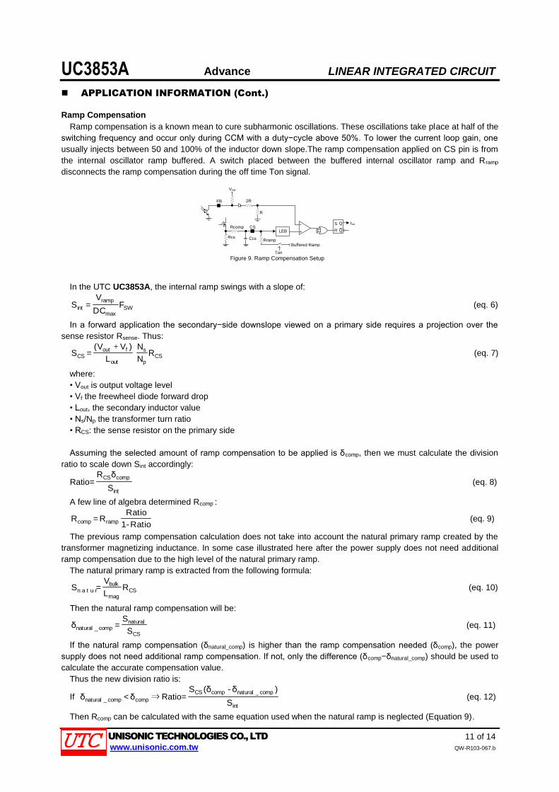
APPLICATION INFORMATION (Cont.)
Ramp Compensation
Ramp compensation is a known mean to cure subharmonic oscillations. These oscillations take place at half of the
switching frequency and occur only during CCM with a duty−cycle above 50%. To lower the current loop gain, one
usually injects between 50 and 100% of the inductor down slope.The ramp compensation applied on CS pin is from
the internal oscillator ramp buffered. A switch placed between the buffered internal oscillator ramp and Rramp
disconnects the ramp compensation during the off time Ton signal.
FB
VDD
2R
R
Buffered RampRramp
LEBCS
Ccs
Rcomp
Rcs
tonS Q
QR
Figure 9. Ramp Compensation SetupTon
In the UTC UC3853A, the internal ramp swings with a slope of:
intS = SWmax
rampF
DC
V (eq. 6)
In a forward application the secondary−side downslope viewed on a primary side requires a projection over the
sense resistor Rsense. Thus:
CSS =out
fout
L
)VV( +CS
p
sR
N
N (eq. 7)
where:
• Vout is output voltage level
• Vf the freewheel diode forward drop
• Lout, the secondary inductor value
• Ns/Np the transformer turn ratio
• RCS: the sense resistor on the primary side
Assuming the selected amount of ramp compensation to be applied is δcomp, then we must calculate the division
ratio to scale down Sint accordingly:
Ratio=int
compCS
S
δR (eq. 8)
A few line of algebra determined Rcomp :
compR =Ratio-1
RatioRramp (eq. 9)
The previous ramp compensation calculation does not take into account the natural primary ramp created by the
transformer magnetizing inductance. In some case illustrated here after the power supply does not need additional
ramp compensation due to the high level of the natural primary ramp.
The natural primary ramp is extracted from the following formula:
n a t u r a lS = CSmag
bulkR
L
V (eq. 10)
Then the natural ramp compensation will be:
comp_naturalδ =CS
natural
S
S (eq. 11)
If the natural ramp compensation (δnatural_comp) is higher than the ramp compensation needed (δcomp), the power
supply does not need additional ramp compensation. If not, only the difference (δcomp−δnatural_comp) should be used to
calculate the accurate compensation value.
Thus the new division ratio is:
If comp_naturalδ < compδ ⇒ Ratio=int
comp_naturalcompCS
S
)δ-δ(S (eq. 12)
Then Rcomp can be calculated with the same equation used when the natural ramp is neglected (Equation 9).
UC3853A Advance LINEAR INTEGRATED CIRCUIT
UNISONIC TECHNOLOGIES CO., LTD 12 of 14
www.unisonic.com.tw QW-R103-067.b
APPLICATION INFORMATION (Cont.)
Ramp Compensation Design Example
2 switch−Forward Power supply specification:
• Regulated output: 12V
• Lout=27μH
• Vf=0.62V (drop voltage on the regulated output)
• Current sense resistor: 0.75Ω
• Switching frequency: 100kHz
• Vbulk=350V, minimum input voltage at which the power supply works.
• Duty cycle max: DCmax=75%
• Vramp=3.5V, Internal ramp level.
• Rramp=26.5kΩ, Internal pull−up resistance
• Targeted ramp compensation level: 100%
• Transformer specification: Lmag=13mH, Ns/Np=0.085 Internal ramp compensation level
intS = ⇒SWmax
rampF
DC
VintS = 00kHz1*
75.0
5.3=467mV/μS
Secondary−side downslope projected over the sense resistor is:
CSS = ⇒+
CSp
s
out
foutR
N
N
L
)VV(CSS = 75.0*085.0
10*27
)7.012(6-
+=30mV/μS
Natural primary ramp:
naturalS = ⇒CSmag
bulkR
L
VnaturalS = 75.0*
1013
3503-•
=20.19mV/μS
Thus the natural ramp compensation is:
comp_naturalδ = ⇒CS
natural
S
Scomp_naturalδ =
30
19.20=67.3%

UC3853A Advance LINEAR INTEGRATED CIRCUIT
UNISONIC TECHNOLOGIES CO., LTD 13 of 14
www.unisonic.com.tw QW-R103-067.b
APPLICATION INFORMATION (Cont.)
Here the natural ramp compensation is lower than the desired ramp compensation, so an external compensation
should be added to prevent sub−harmonics oscillation.
Ratio=int
comp_naturalcompCS
S
)δ-δ(S⇒ Ratio=
467
)673.0-00.1(*30=0.021
We can know calculate external resistor (Rcomp) to reach the correct compensation level.
compR = ⇒Ratio-1
RatioRramp compR =
021.0-1
021.0*10*5.26 3 =568.4Ω
Thus with Rcomp = 570Ω, 100% compensation ramp is applied on the CS pin.
The following example illustrates a power supply where the natural ramp offers enough ramp compensation to
avoid external ramp compensation.
2 switch−Forward Power supply specification:
• Regulated output: 12V
• Lout=27μH
• Vf=0.7V
• Current sense resistor: 0.75Ω
• Switching frequency: 100kHz
• Vbulk=350V, minimum input voltage at which the power supply works.
• Duty cycle max: DCmax =75%
• Vramp=3.5V, Internal ramp level.
• Rramp=26.5kΩ, Internal pull−up resistance
• Targeted ramp compensation level: 100%
• Transformer specification: Lmag=8mH, Ns/Np=0.085
Secondary−side downslope projected over the sense resistor is:
CSS = ⇒+
CSp
s
out
foutR
N
N
L
)VV(CSS = 75.0085.0
1027
)7.012(6-
ו
+=30mV/μS
The natural primary ramp is:
naturalS = ⇒CSmag
bulkR
L
VnaturalS = 75.0
10*8
3503-
=32.8mV/μS
And the natural ramp compensation will be:
c o m p_n a t u r a lδ = ⇒CS
natural
S
Scomp_naturalδ =
30
8.32 ≈110%
So in that case the natural ramp compensation due to the magnetizing inductance of the transformer will be
enough to prevent any sub−harmonics oscillation in case of duty cycle above 50%.

UC3853A Advance LINEAR INTEGRATED CIRCUIT
UNISONIC TECHNOLOGIES CO., LTD 14 of 14
www.unisonic.com.tw QW-R103-067.b
TYPICAL APPLICATION CIRCUIT
Vbulk
1
UTC
UC3853A
2
3
4
8
7
6
5
VCC
Vout
UTC assumes no responsibility for equipment failures that result from using products at values that
exceed, even momentarily, rated values (such as maximum ratings, operating condition ranges, or other
parameters) listed in products specifications of any and all UTC products described or contained herein .
UTC products are not designed for use in life support appliances, devices or systems where malfunction
of these products can be reasonably expected to result in personal injury. Reproduction in whole or in
part is prohibited without the prior written consent of the copyright owner. UTC reserves the right to
make changes to information published in this document, including without limitation specifications and
product descriptions, at any time and without notice. This document supersedes and replaces all
information supplied prior to the publication hereof.