unit 1 · optical fiber communication system: the figure 1.1 shows a block schematic of the...
TRANSCRIPT

UNIT 1
1. What are the various elements of an optical communication system?
Explain each element in brief?
Ans: Optical Fiber Communication System:
The figure 1.1 shows a block schematic of the different elements in an optical fiber
communication system. The carrier is modulated using analog information signal. The variation
of light emitting from the optical source is a continuous signal. The information source provides
an electrical signal to the transmitter. The transmitter comprises electrical stage. The electrical
stage (circuits) drives an optical source. The optical source output is a light which is intensity
modulated by the information. The optical source converts the electrical signal into an optical
signal. The source may be either semiconductor laser or Light Emitting Diode (LED). The
intensity modulated light signal is coupled to fiber. The fiber which is made up of a glass acts as
a channel between the transmitter and receiver.
At the receiver the optical signal is detected by the optical detectors such as PIN diode and
Avalanche photodiode.
Sometimes photo transistors and photo conductors are used for converting an optical signal into
electrical signal. The electrical signal is again processed and given to the transducer to get the
original information.
2. Give the block diagram of a digital optical communication system and
explain the function of each block?
Ans: Digital Fiber optical Communication System:

Figure shows a schematic of a typical digital optic fiber link. The input is given as digital signal
from the information source and it is encoded for optical transmission in the encoder. The
encoder, encodes or modulates the digital signal as in the case of simple communication system
where we are using a message signal in which the signal is in analog form, but here the signal is in
digital form which is encoded i.e., modulated in the encoder. The laser drive circuit directly
modulates the intensity of semiconductor laser with the encoded digital signal. Hence a digital
optical signal is launched into the optical fiber cable. At the receiver we have to decode the digital
optical signal for which we are using another Avalanche Photo Diode (APD) as detector. The
avalanche photo diode detector is followed by a front-end amplifier and equalizer or filter to
provide gain as well as linear signal processing and noise bandwidth reductions. Then the signal is
passed through the decoder to get original digital information which is transmitted
3. Distinguish between optical fiber communication system and conventional
communication system? And List out the advantageous and disadvantage of
optical fiber communication?
Ans:
Optical Fiber Communication System Conventional Communication System
1. Requires a bandwidth of 1013
to 1016
Hz. 1.Requires a bandwidth of 500 MHz
2 .Light weight. 2. Heavier in weight.
3. Immune to R.F. interference. 3. Needs external shielding.
4. Electrical isolation. 4. Exhibits earthing problems.
5. Low loss of about 0.2 dB/km. 5. Loss of about 10dB/km.
6. Secure signal propagation. 6. Signal can be tapped easily.

7.Due to increased bandwidth higher data 7. Low data rates compared to optical fiber.
Advantageous Of Optical Fibers Communication:
1. Information bandwidth is more.
2. Optical fibers are small in size and light weighted.
3. Optical fibers are more immune to ambient electrical noise, electromagnetic interference.
4. Cross talk and internal noise are eliminated in optical fibers.
5. There is no risk of short circuit in optical fibers.
6. Optical fibers can be used for wide range of temperature.
7. A single fiber can be used to send many signals of different wavelengths using Wavelengths
Division Multiplexing (WDM).
8. Optical fibers are generally glass which is made up of sand and hence they are cheaper than
copper cables.
9. Optical fibers are having less transmission loss and hence less number of repeaters are used.
10. Optical fibers are more reliable and easy to maintain.
Disadvantageous Of Optical Fibers Communication:
1. Attenuation offered by the optical fibers depends upon the material by which it is made.
2. Complex electronic circuitry is required at transmitter and receiver.
3. The coupling of optical fibers is difficult.
4. Skilled labors are required to maintain the optical fiber communication.
5. Separated power supply is required for electronic repeaters at different stages.
4. Compare the advantages and disadvantages of guided optical communication lines with that of microwave systems?
Ans:
Optical Communication System Microwave System 1. Uses glass optical fibers or plastic optical 1. Uses co-axial cable or microwave
fibers for transmission. waveguides for transmission.
2. Low weight, hence large transmission 2. Heavier than optical fibers.
distance or same weight of microwave link.
3. Large bandwidth of range 1013
3. Bandwidth is lesser in the range of 108 to
tol016
Hz. 1010
Hz.

4. Electrically isolated, hence no 4. Prone to electrical disturbances and hence,
shielding is required. shielding for reducing RE interference.
5. Low loss of 0.2dB/km. 5. A considerable loss of 5 dB/km.
6. Large spacing between repeaters about 1 in 6. Spacing distance between repeaters is less, is
300 km. suitable only for short distance if waveguides
are used.
7. Because large bandwidth, higher data rate of 7. Data rates of mega bits per second can be
the order of terabits per second. obtained.
8. Message security is obtained. 8. Signal can be tapped easily.
9. No cross talk, hence many fiber 9. If shielding is not done properly, cross talk
communication channels can be packed inside is introduced.
one single cable.
Disadvantages
Optical Communication System Microwave System
1. Expensive transmitter and 1. Simple and less expensive transmitter and
receiver. receiver.
2. Difficult coupling. 2. Easy coupling.
3. Power transmission depends upon the 3. Output power is directly coupled to the
quantum efficiency of light source (LED or transmission line.
LASER).
4. Unable to excite the terminal device 4. Able to operate the terminal device directly.
directly.
5. Write in detail about ray optics?
Ans: Ray optics is used for representing the mechanism of a ray which propagates through an ideal multimode step index optical waveguide. There are two types of rays, the skew rays and meridional rays which propagate through a fiber.
The path of meridional can be tracked very easily as they are confined to a single plane.
Meridional are described in two classes. They are,
(i) Bound rays
(ii) Unbound rays.
Bound rays are those rays which are trapped in a core and they move along the fiber whereas
unbound rays are those rays which get refracted out of the fiber.
Skew rays are those rays which follow helical path but they are not confined to a single plane.
We know that skew rays are not confined to a particular plane so they cannot be tracked easily.
Analyzing the meridional rays is sufficient for the purpose of result, rather than skew rays,
because skew rays lead to greater power loss.
Now coming to ray theory, we need to consider meridional rays. Representation of meridional
rays is given below.

From the medium of refractive index 'n' which is at an angle ‘θ0’with respect to fiber axis, the
light enters the fiber core. If the light strikes at such an angle then it gets reflected internally and
the meridional ray moves in a zig zag path along the fiber core, passing through the axis of the
guide. Now by using Snell's law the minimum angle ‘фmin’ supports total internal reflection for
meridional ray is given by
If the ray strikes the core-cladding interface at an angle less than фmin then they get refracted out
of the core and they will be lost from the cladding.
By applying Snell’s law to the air-fiber face boundaries, we get θmax
nsin θmax = n1 sin θc = (n n )1/2
Where θc = П/2 – θ0 (From the figure)
So, the rays whose entrance angle ‘θ0’ is less than the ‘θmax’ will be reflected back in to core
cladding interface.
Numerical aperture for a step index is given by the formula
N.A = n sin θmax
= (n n )1/2
= n1√2
6. An optical fiber has a NA of 0.20 and a cladding refractive index of 1.59
Determine
(i) The acceptance angle for the fiber in water which has a refractive index of
1.33
(ii) Critical angle at the core cladding interface.
Ans:
Given
NA = 0.2
n1 =1.59
(i) The acceptance by the water is
Refractive index for water n =1.33
NA = n sin θa
θa = sin-1
(NA/n) = sin-1
(0.2/1.59) = 8.640
Therefore the acceptance angle is = 8.640
(ii)Critical angle at core cladding interface is
We know that,
NA= ( thatn)
1/2
We knownn
NA = 0.2 and n1 =1.59
0.2 = (
n )
1/2
0.447 =1.59
( )
=2.0811.59
n
nn2 = 1.44
θc= n sin-1
(n2/ n1) = 1.33 sin-1
(1.44/ 1.59) = 86.330
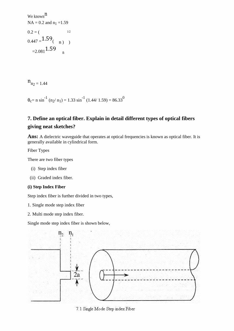
7. Define an optical fiber. Explain in detail different types of optical fibers
giving neat sketches?
Ans: A dielectric waveguide that operates at optical frequencies is known as optical fiber. It is generally available in cylindrical form.
Fiber Types
There are two fiber types
(i) Step index fiber
(ii) Graded index fiber.
(i) Step Index Fiber
Step index fiber is further divided in two types,
1. Single mode step index fiber
2. Multi mode step index fiber.
Single mode step index fiber is shown below,
The typical dimension of core is 8 to 12 μm and cladding is 125 μm.
In step index fiber, the refractive index of the core is uniform and at the cladding boundary, it
undergoes a step change.
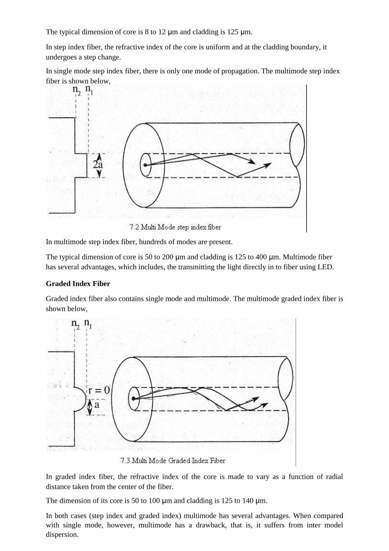
In single mode step index fiber, there is only one mode of propagation. The multimode step index
fiber is shown below,
In multimode step index fiber, hundreds of modes are present.
The typical dimension of core is 50 to 200 μm and cladding is 125 to 400 μm. Multimode fiber
has several advantages, which includes, the transmitting the light directly in to fiber using LED.
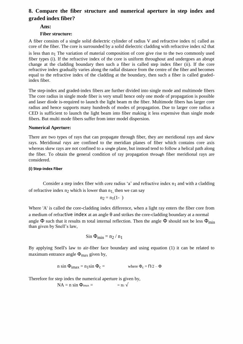
Graded Index Fiber
Graded index fiber also contains single mode and multimode. The multimode graded index fiber is
shown below,
In graded index fiber, the refractive index of the core is made to vary as a function of radial
distance taken from the center of the fiber.
The dimension of its core is 50 to 100 μm and cladding is 125 to 140 μm.
In both cases (step index and graded index) multimode has several advantages. When compared
with single mode, however, multimode has a drawback, that is, it suffers from inter model
dispersion.
8. Compare the fiber structure and numerical aperture in step index and
graded index fiber?
Ans:
Fiber structure:
A fiber consists of a single solid dielectric cylinder of radius V and refractive index n{ called as core of the fiber. The core is surrounded by a solid dielectric cladding with refractive index n2 that
is less than n1 The variation of material composition of core give rise to the two commonly used
fiber types (i). If the refractive index of the core is uniform throughout and undergoes an abrupt change at the cladding boundary then such a fiber is called step index fiber (ii). If the core refractive index gradually varies along the radial distance from the centre of the fiber and becomes equal to the refractive index of the cladding at the boundary, then such a fiber is called graded-index fiber.
The step-index and graded-index fibers are further divided into single mode and multimode fibers
The core radius in single mode fiber is very small hence only one mode of propagation is possible
and laser diode is-required to launch the light beam m the fiber. Multimode fibers has larger core
radius and hence supports many hundreds of modes of propagation. Due to larger core radius a
CED is sufficient to launch the light beam into fiber making it less expensive than single mode
fibers. But multi mode fibers suffer from inter model dispersion.
Numerical Aperture:
There are two types of rays that can propagate through fiber, they are meridional rays and skew
rays. Meridional rays are confined to the meridian planes of fiber which contains core axis
whereas skew rays are not confined to a single plane, but instead tend to follow a helical path along
the fiber. To obtain the general condition of ray propagation through fiber meridional rays are
considered.
(i) Step‐index Fiber
Consider a step index fiber with core radius ‘a’ and refractive index n1 and with a cladding
of refractive index n2 which is lower than n1, then we can say
n2 = n1(1- )
Where 'A' is called the core-cladding index difference, when a light ray enters the fiber core from
a medium of refractive index at an angle θ and strikes the core-cladding boundary at a normal angle Φ such that it results m total internal reflection. Then the angle Φ should not be less Φmin than given by Snell’s law,
Sin Φmin = n2 / n1
By applying Snell's law to air-fiber face boundary and using equation (1) it can be related to
maximum entrance angle Φmax given by,
n sin Φimax = n1sin Φc = where Φc = П/2 – Φ
Therefore for step index the numerical aperture is given by, NA = n sin Φimax = = n1 √

(ii) Graded-Index Fiber
For a graded index fiber the refractive index difference is given by,
= =
is approximately equal in both step-index fiber and graded index fiber.
Numerical aperture of graded index fiber is a function of position across, the case end face,
whereas, NA is step-index is constant across the core. The light incident on the fiber core at
position r will propagate through fiber only if it is within the local numerical aperture of the fiber
at that position given by,
NA(r) =
Where, r is the radial distance from the centered the fiber V is the radius of core a is dimensionless
parameter defining the shape of index profile and NA(0) is axial numerical aperture defined as,
NA(0) = (n2(0) - n )
1/2
from centre to core-cladding boundary i.e., at centre NA is equal to that of step index and
gradually reduces until it becomes zero at the core-cladding boundary.
9. Give three applications of optical fiber in instrumentation and explain them
with necessary figure?
Ans: Optical fibers are used as sensing-elements(sensors) in instrumentation applications. Since, they have the advantage of efficient telemetry and control communication they can also work in electrically harsh environments and are free from EM interference. The optical fiber sensor system modulates a light beam either directly or indirectly by the
parameters like temperature, pressure, displacement, strain etc. Modulation is done in the
modulation zone of the optical fiber sensor system as shown in figure 9.1. The light beam is
modulated in any of its parameters, which includes optical intensity, phase, polarization,
wavelength and spectral distribution.
(i) Optical Fluid Level Detector

Figure (9.2) shows the functioning of a simple optical fluid level detector. It contains an
optical source, optical detector, optical dipstick and fluid. The optical dipstick is formed by glass
(with refractive index μ1) and fluid has a refractive index μ2. The refractive index of fluid is
greater than refractive index of optical dipstick (μ1 > μ2). When the fluid does not touch the optical dipstick the light beam from optical source passes through the glass as shown in figure 9.2(a). When the fluid touches the chamfered end, total internal reflection halts and the light is transmitted into the fluid as shown in figure 9.2(b). As a result, an indication of the fluid level is acquired at the optical detector.
(ii) Optical Displacement Detector
This is also implemented as extrinsic device. The received light ray is modulated by
intensity. The reflected light from the target is received and the intensity of received light is
proportional to distance/displacement of target. Thus, displacement is measured.
(iii) Optical Fiber Flow Meter This is implemented as intrinsic device, where the flow rate itself causes the modulation of
light. A multimode fiber is placed along the cross-section of flow pipe, so that liquid flow pass the
fiber. Presence of fiber causes turbulence in the liquid flow as a result fiber oscillates and frequency of oscillation is directly proportional to flow rate. This oscillation gives a modulated light at the receiver. Thus, flow rate is measured

10. A single Mode step index fiber has a core diameter of 7μm and core
refractive index of 1.49.Estimate the shortest wavelength of light which allows
single mode operation when the refractive index difference for the fiber is 1% ?
Ans;
Given that
For a single mode step index fiber,
n1 = 1.49
2a = 7μm => a = 3.5 μm
= 0.01
We have
n2 = n1 (1- )
= 1.49(1-0.01)
= 1.4751
Therefore n2 =1.48
The condition to be fulfilled for a fiber to be single mode is that normalized frequency, V ≤ 2.4
i.e., By using this relation,
V = П n n
2.4 = П
2.4 = П .
n n
1.49 1.48
λ = 1.58μm.

UNIT- 2
1. List the requirements that be satisfied by materials used to manufacture
optical fiber?
ANS: Fiber Materials
Most of the fibers are made up of glass consisting of either Silica (SiO2) or .Silicate. High-
loss glass fibers are used for short -transmission distances and low -loss glass fibers are used for
long distance applications. Plastic fibers are less used because of their higher attenuation than
glass fibers. Glass Fibers The glass fibers are made from oxides. The most common oxide is silica whose refractive
index is 1.458_at 850 nm. To get different index fibers, the dopants such as GeO2, P2O5 are added
to silica. GeO2 and P2O3 increase the refractive index whereas fluorine or B203 decreases the refractive index. Few fiber compositions are given below as follows,
(i) GeO2 – SiO2 Core: SiO2 Cladding (ii) P2Q5 – SiO2, Core; SiO2 Cladding
The principle raw material for silica is sand. The glass composed of pure silica is referred to as
silica glass, nitrous silica or fused silica. Some desirable properties of silica are,
(i) Resistance to deformation at temperature as high as 1000°C.
(ii) High resistance to breakage from thermal shock.
(iii) Good chemical durability.
(iv) High transparency in both the visible and infrared regions.
Basic Requirements and Considerations in Fiber Fabrication
(i) Optical fibers should have maximum reproducibility.
(ii) Fibers should be fabricated with good stable transmission characteristics i.e., the fiber
should have invariable transmission characteristics in long lengths. (iii) Different size, refractive index and refractive index profile, operating wavelengths
material. Fiber must be available to meet different system applications. (iv) The fibers must be flexible to convert into practical cables without any degradation of
their characteristics. (v) Fibers must be fabricated in such a way that a joining (splicing) of the fiber should not
affect its transmission characteristics and the fibers may be terminated or connected
together with less practical difficulties.
Fiber Fabrication in a Two Stage Process
(i) Initially glass is produced and then converted into perform or rod.
2. Write in detail about glass fiber and detail about plastic optical fiber?
Ans: Glass fiber is a mixture of selenides, sulfides and metal oxides. It can be classified into,
1. Halide Glass Fibers 2. Active Glass Fibers 3. Chalgenide Glass Fibers.
Glass is made of pure SiO2 which refractive index 1.458 at 850 nm. The refractive index of SiO2
can be increased (or) decreased by adding various oxides are known as dopant.
The oxides GeO2 or P2O3 increases the refractive index and B2O3 decreases the refractive index
of SiO2 The various combinations are,
(i) GeO2 SiO2 Core; SiO2 cladding
(ii) P2 O3 – SiO2 Core; SiO2 cladding
(iii) SiO2 Core; B2O3, - SiO2 cladding
(iv) GeO2- B2O3- SiO2, Core; B2O3 - SiO2 cladding.
From above, the refractive index of core is maximum compared to the cladding.
(1) Halide Glass Fibers
A halide glass fiber contains fluorine, chlorine, bromine and iodine. The most common
Halide glass fiber is heavy "metal fluoride glass". It uses ZrF4 as a major component. This
fluoride glass is known by the name ZBLAN. since it is constituents are ZrF4, BaF2, LaF3 A1F3, and NaF
The percentages of these elements to form ZBLAN fluoride glass is shown as follows,
Materials Molecular percentage
ZrF4 54%
20%
BaF2
4.5%
LaF3
3.5%
A1F3
18%
NaF
These materials add up to make the core of a glass fiber. By replacing ZrF4 by HaF4, the lower
refractive index glass is obtained.
The intrinsic losses of these glasses is 0.01 to 0.001 dB/km
(2) Active Glass Fibers Active glass fibers are formed by adding erbium and neodymium to the glass fibers. The above
material performs amplification and attenuation

(3) Chalgenide Glass Fibers
Chalgenide glass fibers are discovered in order to make use of the nonlinear properties of
glass fibers. It contains either "S", "Se" or "Te", because they
are highly nonlinear and it also contains one element from “Cl”, "Br”, “Cd”,”Ba” or”Si”.
The mostly used chalgenide glass is AS2- S3, AS40S58Se2 is used to make the core and AS2S3
is used to make the cladding material of the glass fiber. The insertion loss is around 1 dB/m.
Plastic Optical Fibers Plastic optical fibers are the fibers which are made up of plastic material. The core of this
fiber is made up of Polymethylmethacrylate (PMMA) or Perflourmated Polymer (PFP).
Plastic optical fibers offer more attenuation than glass fiber and is used for short distance
applications. These fibers are tough and durable due to the presence of plastic material. The
modulus of this plastic material is two orders of magnitude lower than that of silica and even a 1
mm diameter graded index plastic optical fiber can be installed in conventional fiber cable routes.
The diameter of the core of these fibers is 10-20 times larger than that of glass fiber which
reduces the connector losses without sacrificing coupling efficiencies. So we can use inexpensive
connectors, splices and transceivers made up of plastic injection-molding technology.
Graded index plastic optical fiber is in great demand in customer premises to deliver high-speed
services due to its high bandwidth
3. What are the basic attenuation mechanisms in the optical fiber
communication? Explain in brief on what factors this mechanism depends?
Ans: Attenuation When a decrease in light power occurs during light propagation along an optical fiber then such a
phenomenon is called attenuation. The major causes for attenuation in fiber optic
communications are, 1. Bending loss 2. Scattering loss 3. Absorption loss 1. Bending Loss Bending loss is further classified into,
(i) Macro bending loss-and (ii) Micro bending loss.
(i) Macro bending Loss The light travels in fiber due to occurrence of total internal reflection inside the fiber at the
interface of core and cladding. However the light beam forms a critical angle with the fiber's
central axis at the fiber face. When the fiber is bend and the light beam travelling through fiber
strikes at the boundary o f core at an angle greater than critical angle then the beam fails to
achieve total internal reflection. Hence this beam is lost through the cladding.
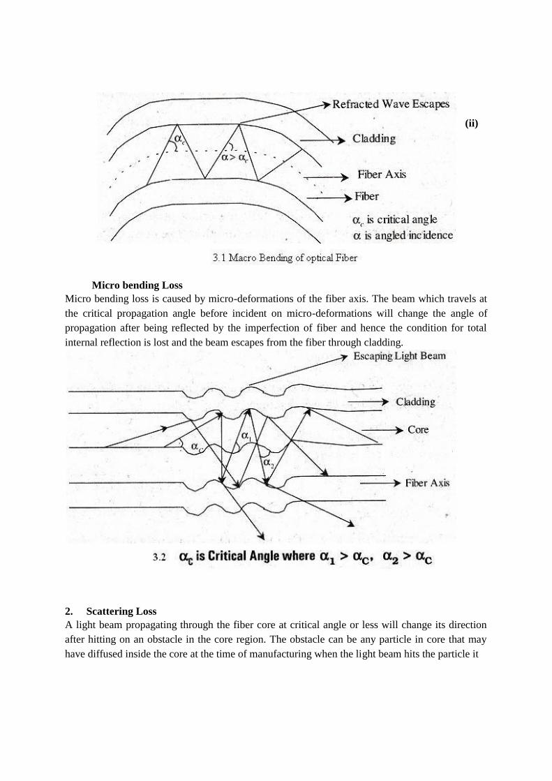
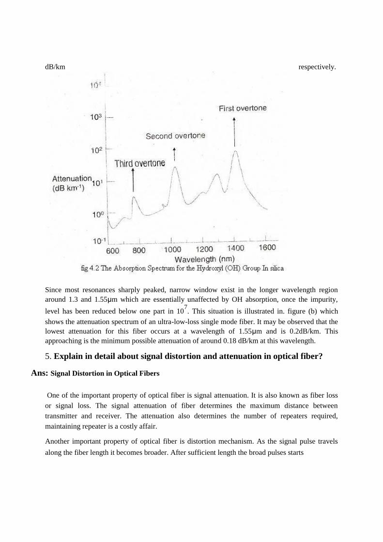
(ii)
Micro bending Loss Micro bending loss is caused by micro-deformations of the fiber axis. The beam which travels at
the critical propagation angle before incident on micro-deformations will change the angle of
propagation after being reflected by the imperfection of fiber and hence the condition for total
internal reflection is lost and the beam escapes from the fiber through cladding.
2. Scattering Loss A light beam propagating through the fiber core at critical angle or less will change its direction
after hitting on an obstacle in the core region. The obstacle can be any particle in core that may
have diffused inside the core at the time of manufacturing when the light beam hits the particle it

get scattered and due to this total internal reflection is not achieved hence, the beam is lost through
the cladding.
3. Absorptions Loss Whenever a beam of light photon having energy equal to energy band gap then the light photon is
absorbed by the material resulting in absorption loss. Absorption loss occur due to presence of
anions OH~ in silica fibers and due to metallic ions like Iron (Fe), Chromium (Cr) and Nickel
(Ni). The absorption loss peak is observed in the region of 2700 nm and 4200 nm wavelength with
low-loss at 7200 nm, 9500 nm and 13800 nm wavelength windows.
4. Explain in detail about ultra sonic absorption, infrared absorption and ion
resonance absorption losses in the pure and doped SiO2 at various levels?
Ans: An absolutely pure silicate glass has little intrinsic absorption due to its, basic material
structure in the near infrared region. However it does have two major intrinsic absorption
mechanisms at optical wavelengths as illustrated in the following figure which shows a possible
optical attenuation against wavelength characteristic for absolutely pure glass (i.e., SiO2). There is
a fundamental absorption edge, the peaks of which are centered in the ultraviolet wavelength
region. This is due to the stimulation of electrons transitions within the glass by higher energy
excitation. The tail of this peak may extend into the window region at the shorter wavelengths.
Also in the infrared and far-infrared, normally at wavelengths above 7μm. Absorption bands from
the interaction of photons with molecular variations within the glass occur. These give

absorption peaks which again extend into the window region. Hence, above 1.5μm, the tails of
these largely far-infrared absorption peaks tend to increase the pure glass losses.
In practical optical fibers prepared by conventional melting techniques, a major source of signal
attenuation is extrinsic (doped) absorption from transition metal element impurities. Certain
impurities, namely Chromium and Copper, in their worst valence state can cause attenuation is
excess of 1 dB/km in the near infrared region. Transition element contamination may be reduced
to acceptable levels i.e., one part is 1010 by glass refining techniques such as vapor -phase
oxidation. It may also be observed that the only significant absorption band in the region below a
wavelength of 1urn is the second overtone at 0.95 am which causes attenuation of about 1 dB/km
for one part per million (ppm) of hydroxyl. At longer wavelengths the first overtone at 1.38 urn
and its side band at 1.24 am are strong absorbers giving attenuation of about 2 dB/km ppm and 4
dB/km respectively.
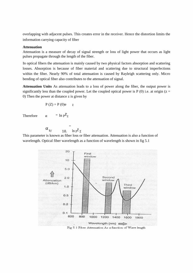
Since most resonances sharply peaked, narrow window exist in the longer wavelength region
around 1.3 and 1.55μm which are essentially unaffected by OH absorption, once the impurity,
level has been reduced below one part in 107. This situation is illustrated in. figure (b) which
shows the attenuation spectrum of an ultra-low-loss single mode fiber. It may be observed that the
lowest attenuation for this fiber occurs at a wavelength of 1.55μm and is 0.2dB/km. This
approaching is the minimum possible attenuation of around 0.18 dB/km at this wavelength.
5. Explain in detail about signal distortion and attenuation in optical fiber?
Ans: Signal Distortion in Optical Fibers
One of the important property of optical fiber is signal attenuation. It is also known as fiber loss
or signal loss. The signal attenuation of fiber determines the maximum distance between
transmitter and receiver. The attenuation also determines the number of repeaters required,
maintaining repeater is a costly affair.
Another important property of optical fiber is distortion mechanism. As the signal pulse travels
along the fiber length it becomes broader. After sufficient length the broad pulses starts
overlapping with adjacent pulses. This creates error in the receiver. Hence the distortion limits the
information carrying capacity of fiber
Attenuation Attenuation is a measure of decay of signal strength or loss of light power that occurs as light
pulses propagate through the length of the fiber.
In optical fibers the attenuation is mainly caused by two physical factors absorption and scattering
losses. Absorption is because of fiber material and scattering due to structural imperfections
within the fiber. Nearly 90% of total attenuation is caused by Rayleigh scattering only. Micro
bending of optical fiber also contributes to the attenuation of signal.
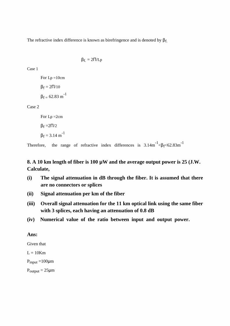
Attenuation Units As attenuation leads to a loss of power along the fiber, the output power is
significantly less than the coupled power. Let the coupled optical power is P (0) i.e. at origin (z =
0) Then the power at distance z is given by
P (Z) = P (0)e Z
Therefore α
ln PP Z
α B/ 10.
ln PP Z
This parameter is known as fiber loss or fiber attenuation. Attenuation is also a function of
wavelength. Optical fiber wavelength as a function of wavelength is shown in fig 5.1

6. Explain the following
(i) Mode field diameter
(ii) Modal Birefringence
ans:
Mode field diameter:
Mode field diameter is\a primary parameter of single-mode fibers. It is obtained from the
mode field distribution of the fundamental mode.
The figure shows, the distribution of light in a single mode fiber.
In order to find the MFD for field intensity E2(r) must be calculated by using E
2(r) MFD can
be calculated as,
MFD = 2ω0
= 2
Where
.
2ω0 = spot size
To avoid complexity, E(r) can be taken as,
E(r) = E (0) exp (r2/ ω0
2)
Where r= radius

E (0) = field at (r=0)
By using this relation, we can write
MFD = 1/e2 width of optical power.
(ii) Modal Birefringence
The propagation of two approximately degenerate modes with orthogonal polarizations is allowed
in single mode fibers with nominal circular symmetry about the core axis. Thus, these are referred
as bimodal supported and modes. Here, the super scripts x and y denotes the principle axes and are
calculated using the symmetry elements of the fiber cross section. The difference in the effective
refractive indices and phase velocities for these orthogonally polarized modes makes the fiber to
function as a birefringent medium. The independency of fiber cross section with the fiber length in
the z-direction yields the expression for modal birefringence BF as,
Where, βx = Propagation constant for the mode„x‟ βy= Propagation constant for the mode 'y'
λ = Optical wavelength.
The difference in phase velocities is responsible for linear retardation Φ (z) exhibited by the
fiber. The expression for linear retardation is given by,
Φ (z) = (βx – βy) L
Where,
L = Length of the fiber. If the coherence time of the source is greater than the delay between the two transit times then
only, the phase coherence of the two mode components is achieved. However, the expression for
coherence time of the source is given by,
tc = 1/ δf
Where, δf = Uncorrelated source frequency width
Then, the length of fiber over which birefringent coherence is maintained is given by Where, c = Velocity of light in vacuum
δλ = Source line width

Figure 6.1 illustrates the variations of polarization state periodically along the fiber
The characteristic length LB corresponding to the above process is referred as beat length and is
given by,
LB = λ/BF……………….. (5)
From equation (1), we have
LB = П …………. (6)
And expression 2 can be written as.
Φ (LB) = (βx – βy) LB
= (βx – βy) П = 2П………….. (7)
Based on the above observation of beat length, we can determine the modal birefringence BF.
7. Commonly available single mode fiber have beat length in the range
10cm<LP<2m .What rate of refractive index difference does this corresponds
to for λ =1300nm?
Ans:
Give that
For a single mode fiber,
Beat length LP = 10cm to 2cm
Operating wavelength λ = 1300nm
The refractive index difference is known as birefringence and is denoted by βf.
βf. = 2П/Lp
Case 1
For Lp =10cm
βf = 2П/10
βf = 62.83 m-1
Case 2
For Lp =2cm
βf =2П/2
βf = 3.14 m-1
Therefore, the range of refractive index differences is 3.14m-1
<βf<62.83m-1
8. A 10 km length of fiber is 100 μW and the average output power is 25 (J.W.
Calculate,
(i) The signal attenuation in dB through the fiber. It is assumed that there
are no connectors or splices
(ii) Signal attenuation per km of the fiber
(iii) Overall signal attenuation for the 11 km optical link using the same fiber
with 3 splices, each having an attenuation of 0.8 dB
(iv) Numerical value of the ratio between input and output power.
Ans:
Given that
L = 10Km
Pinput =100μm
Poutput = 25μm

(i) Attenuation
(αdB) = 10 log10 (Pinput/ Poutput)
αdB = 10 log10
αdB = 6.02dB.
(ii) The signal attenuation per Km of the fiber is,
αdB.L =6.02
αdB = 6.02/10
αdB =0.602dBKm-1
9. A 10 km length of fiber is 100 μW and the average output power is 25 (J.W.
Calculate,
(i) The signal attenuation in dB through the fiber. It is assumed that there are no connectors or splices
(ii) Signal attenuation per km of the fiber (iii) Overall signal attenuation for the 11 km optical link using the same fiber
with 3 splices, each having an attenuation of 0.8 dB
(iv) Numerical value of the ratio between input and output power. Ans:
Given L=10
Pinput = 100μm
Poutput =25μm
(i) Attenuation
( α) dB =10 log10 (Pinput/Poutput)
α(dB) = 10 log10(100*10-6
/25*10-6
)
α (dB) =6.02 dB

(ii) The signal Attenuation per Km of the fiber is
α (dB) .L =6.02
α (dB) = 6.02/10 dBKm-1
= 0.602 dBKm-1
(iii) Attenuation per unit length α (dB)
The loss produced along 11Km of the fiber is,
α (dB) .L = 0.602*11(Km* dBKm-
1) = 6.622dB
The number of splices are 3, each having attenuation of 0.8 dB
Therefore Total loss due t splices is 0.8*3 =2.4
Therefore Total signal attenuation = 6.622 dB + 2.4dB
α (dB) = 9.022dB
(iv) Numerical values of the ratio between input and output power is,
Pinput/Poutput = 10
B
= 10 . = 7.98
10. A graded index fiber with a parabolic refractive index profile core has a
refractive index at the core axis of 1.5 and a relative index difference of 1%
.Estimate the maximum possible core diameter which allows single mode
operation at a wave length of 1.3μm?
Ans: Given that,
For a graded index fiber with parabolic refractive index profile,
Refractive index of core is n1=1.5.
Relative index difference, = 1% = 0.01
Operating wave length, λ =1.3μm
Maximum possible core diameter = 2a =?

For a graded index fiber, we have,
=
n 2n
n2 =
n2 = 1.485
2 1.5
0.01
n =
2 √1.5
we have,
V =
П
For a single mode operation V ≤ 2.4
n n
2.4 ≥ П
n n
a ≤
П .
.
.
a ≤ 2.346μm
Where a is the radius of the core.
Therefore the maximum possible diameter of the of the core is given by,
2amax = 4.692μm

UNIT 3
1. Write notes on broadening of pulse in the fiber dispersion? Ans: The dispersion of the transmitted optical signal causes distortion for both digital and analog
transmission along optical fibers. If we consider the major implementation of optical fiber
transmission which involves some form of digital modulation, then the dispersion technique
within the fiber causes broadening of the transmitted light pulses as they travel along the channel.
This phenomenon is depicted in figure (a), where it may be observed that each pulse broadens and
coincides with its neighbors, eventually becoming indistinguishable at the receiver input
.
The effect of overlapping of pulses shown in figure (a)' is called Inter Symbol Interference (ISI). Thus, ISI becomes more pronounced when increasing numbers of errors are encountered on the digital optical channel
1

For no overlapping of pulses down on an optical fiber link, the digital bit rate BT must be
less than the reciprocal of the broadened pulse duration through dispersion (2τ) and hence,
BT ≤ 1/2τ…………….. (1)
Equation (1) assumes that the pulse broadening due to dispersion on the channel is T which
follows the input pulse duration which is also τ.
Another more accurate estimate of the maximum bit rate for an optical channel with
dispersion may be obtained by considering the light pulses at the output to have a Gaussian shape
with an r.m.s. width of τ.
2. Explain group delay or time delay in fiber optics? Ans: Modulating signal of an optical source enhances all the modes of fiber equally. This results
in carrying of equal amount of energy by each and every mode of fiber. Since each mode contains
all the spectral components in the wavelength band over which the source emits, hence the
modulating signal modulates every spectral component equally. The signals propagating through
these spectral components experience a time delay or group delay per unit length in the direction
of propagation and it is given as,
D V C ПC
Here D = Distance travelled by the pulse
β = Propagation constant along fiber axis
k = 2П/λ V = Velocity with which the energy in a pulse travels along a fiber
V = C =
From equation (2) we can say that group delay is a function of wavelength 'λ', therefore each
spectral component of any particular mode takes different time to travel a particular distance. This causes difference in time delays and spreading of pulse with time as it travels along the fiber.
The variations in group delay causes pulse spreading. If the spectral width of the optical source is
quite wide, then the delay difference per unit wavelength over the propagation path is given as
The total delay 8x over a distance 'D' for the spectral components which are δλ apart and
δλ/2 above and below a central wavelength 'λc’ is,
δτ = dλ = ПDC 2λ λ δλ
2
3. Explain about fiber optic connectors and types of connectors in detail?
Ans: Fiber Optic Connectors: Connectors are mechanisms or techniques used to join an optical fiber to another fiber or to a fiber
optic component. Different connectors with different characteristics, advantages and disadvantages and performance
parameters are available. Suitable connector is chosen as per the requirement and cost. Various fiber optic connectors from different manufacturers are available SMA 906, ST, Biconic,
FC, D4, HMS-10, SC, FDDI, ESCON, EC/RACE, Principles of good connector design
1. Low coupling loss. 5. Low cost.
2. Inter-changeability. 6. Reliable operation.
3. Ease of assembly. 7. Ease of connection.
4. Low environmental sensitivity. Connector Types Connectors use variety of techniques for coupling such as screw on, bayonet-
mount, push-pull configurations, butt joint and expanded beam fiber connectors.
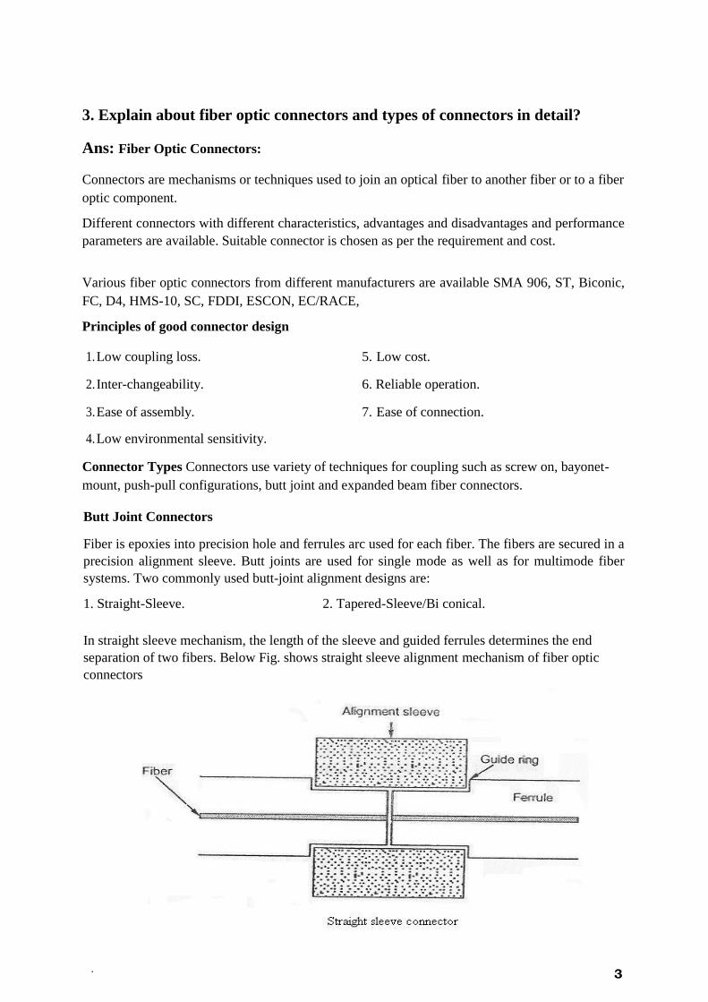
Butt Joint Connectors Fiber is epoxies into precision hole and ferrules arc used for each fiber. The fibers are secured in a
precision alignment sleeve. Butt joints are used for single mode as well as for multimode fiber
systems. Two commonly used butt-joint alignment designs are: 1. Straight-Sleeve. 2. Tapered-Sleeve/Bi conical.
In straight sleeve mechanism, the length of the sleeve and guided ferrules determines the end
separation of two fibers. Below Fig. shows straight sleeve alignment mechanism of fiber optic
connectors
. 3

In tapered sleeve or bi conical connector mechanism, a tapered sleeve is used to accommodate
tapered ferrules. The fiber end separations are determined by sleeve length and guide rings. The
below figure shows tapered sleeve fiber connectors
4. A multi mode graded index fiber exhibits the pulse broadening of 0.2μs over
a distance of 15Km.Estimate, (i) Optimum bandwidth of the fiber
(ii) Dispersion per unit length
(iii)Band width length product Ans:
Given that,
For a multimode graded index fiber,
Total pulse boarding, τ = 0.2μs
Distance, L =15km
(i) The maximum possible optical bandwidth is equivalent to the maximum possible bit rate
assuming no inter symbol interference (ISI) and is given by
Bopt =BT= 1/2τ
= 1/ (2*0.2*10-6
)
= 2.5 MHz
Therefore Bopt = 2.5MHz
(ii) The dispersion per unit length may be acquired by dividing the total dispersion by total length
of the fiber i.e,
Dispersion per unit length = Total dispersion / Total length of fiber
4

= τ/L
= (0.2*10-6
)/15
=13.33ns Km-1
Therefore Dispersion per unit length =13.33ns Km-1
(iii) The band width length product may be obtained by simple multiplying the maximum band
width for the link by its length as,
Bopt .L= 2.5 *106 *15
= 37.5 MHz Km
Alternately, the band width product may be obtained from the dispersion per unit length as,
Bopt .L = 1/ (2*Dispersion per unit length
= 1/ (2*1.33*10-9
)
= 37.5MHz.Km
5. Compare the optical parameters of free space with dispersive and non
dispersive mediums?
Ans: The basic optical properties of light are, (i) Propagation: Light travels along a straight line in a uniform median. (ii) Reflection: It occurs at the surface or boundary of a medium. (iii) Refraction (or bending): It may occur where a change of speed is experienced. (iv) Interference: It is found where two waves are superposed. (v) Diffraction: It happens around a corner when a wave passes the edge of one obstacle.
Dispersive Medium
Glass is an example of dispersive medium. Non uniform bending of different wavelength of light
when it travels along the medium is called dispersion. And the medium in which dispersion takes
place is called dispersive medium.
For a uniform dispersive medium the light wave travels along a straight line. If the medium is non-
uniform and if its density increases as the light wave travels, then the light waves tends to bend
itself towards the normal and vice-versa. Hence, refraction of light waves takes place in dispersive
non uniform medium. Also, in dispersive medium the group velocity and phase velocity is not
constant as a result of interference of different wave fronts travelling at an angle to each other.
Hence refraction takes place. If a plane wave hits an obstacle placed perpendicular to the direction
of its propagation with a pin hole in the centre then the plane wave front is changed into spherical
wave front due to diffractions of light wave through the pin hole
Non-dispersive Medium
Vacuum is an example of non-dispersive medium. In vacuum the light wave travels in straight
line. The group velocity as well as phase velocity of the light wave ii constant. Hence no
refraction takes place in phase vacuum. As the waves travel in straight lines and are parallel to
each other no interference takes place vacuum is free of obstacles. Hence, no diffraction of light
wave takes place.
5
6. Derive the expression for the phase velocity, group velocity using electric
field distribution along the fiber?
Ans: Phase velocit y: All electromagnetic waves which travel along a waveguide have points of
constant phase. As a monochromatic light wave propagates along a waveguide in z-direction, this
point of constant phase travel at particular velocity termed as phase velocity. It is denoted by Th erefore
Where ω = angular frequency of the wave and
β = Phase propagation constant Group Velocity: Group of waves with closely similar frequencies propagate along the waveguide so that there
exists a resultant in the form of packet of waves. This wave packet moves at a velocity termed as
group velocity
=
The formation of wave packets from combination of waves of nearly equal frequencies is, Propagation constant can be given as,
β = n1 (2П/λ) = (n1 ω)/c
where n1= Refractive index of medium Phase velocity c an b e g i v e n a s
8. Write a short notes on dispersion shifted fiber and dispersion compensating
fiber? Ans: Dispersion Shifted Fiber Single mode fibers which are designed to offer simultaneously zero dispersion and minimum
attenuation at λ = 1.55μ m is called dispersion shifted fibers. The dispersion classifications of
various fibers are shown in figure 8.1, which depicts the shifting of zero dispersion wavelength
from λ = 1.33 um to λ= 155 mm. This can be achieved by changing the fiber parameters, namely,
the refractive index dispersion shifted fiber. For example, by reducing the fiber core diameter from 8-10μm to 4.5μm and increasing the
refractive index difference between core and cladding from 0.003 to greater than 0.01 yields zero
dispersion wavelength shifted from 1.33μm to 1.55μm. This may lead to substantial excess loss.
Triangular core profile also yields dispersion shifted fibers and moreover it solves the above
excess loss problem. So, for better results we have to modify the triangular profile. These Profiles are shown in below figure
6
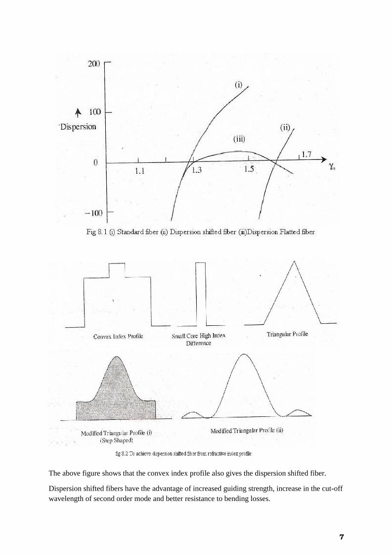
The above figure shows that the convex index profile also gives the dispersion shifted fiber. Dispersion shifted fibers have the advantage of increased guiding strength, increase in the cut-off
wavelength of second order mode and better resistance to bending losses.
7

Such dispersion shifted fibers have been produced by BTRL and others and are now commercially
available from any glass company. Table (1) compares the characteristics of triangular refractive index profile dispersion shifted fiber
with that of simple step index fiber. Step-index Fiber Dispersion shifted fiber(Triangle RI) Attenuation 0.200-0.22 (dB/Km)
Dispersion 17 -180.1 ps(km-nm)
Table (1): Fiber parameters at 1.55 mm Dispersion Compensating Fiber
The process of dispersion compensation and the fiber loop is referred as dispersion compensating
fiber. A large base of dispersion shifted fiber has been installed throughout the world for use in
the single wavelength transmission systems. For these kinds of links the complexity arises from
Four Wave Mixing (FWM), when one attempt to upgrade them with high speed dense WDM
technology in which the channel spacing is less than 100 GHz and the bit rates are in excess of 2.5
Gb/s. By using the passive dispersion compensation technique we can reduce the effect of FWM
(four wave mixing). This consists of inserting into the link a loop of fiber having a dispersion
characteristic that negates the accumulated dispersion of the transmission fiber. This process is
known as dispersion compensation. If the transmission fiber has a low positive dispersion, the
dispersion compensating fiber will have a large negative dispersion. By using this technique, the
total accumulated dispersion will become zero after some distance, but the absolute dispersion per
length is non-zero at all points along the fiber.
Figure depicts the Dispersion Compensating Fiber (DCF) which can be inserted at either the
starting (or) the end of an installed fiber span between two optical amplifiers. A third option is to
have DCF (Dispersion Compensating Fiber) at both ends.
8

In pre-compensation schemes, the DCF is located just after the optical amplifier and just before the
transmission fiber. Where as in post compensation schemes, the DCF is located just after the
transmission fiber and just before the optical amplifier. Above Figure also depicts the plots of
accumulated dispersion and optical power level as functions of distance along the fiber. This figure is
known as dispersion and power maps respectively.
9. How to connect two fibers in a low manner? Explain?
Ans: Interconnection of Two Fibers in a Low Loss Manner The major factor in any fiber optic system is the requirement to interconnect fibers in a low loss
manner. These interconnections occur in three stages namely.
1. At the optical source
2. At the photo detector
3. At intermediate points. 1. Optical Sources The optical sources such as Light Emitting Diodes (LEDs), Solid state lasers and semiconductor
injection lasers are used because of their efficiency, low cost, longer life, sufficient power output,
compatibility and ability to give desired modulations. 2. Photo Detectors Photo detectors such as semiconductor photodiodes are used because of their high quantum
efficiency, adequate frequency response, low dark current and low signal impedance. 3. Intermediate Points The two fibers are joined at intermediate points with two cables within a cable. The two major methods for the interconnection of fibers in a low loss manner are as follows,
(i) Fiber Splices
(ii) Simple Connectors.
(i) Fiber splices In this, the fiber splices are the semi permanent (or) permanent joints which are mostly used for
interconnection in optic-telecommunication system. (ii) Simple Connectors Simple connectors are the removable joints which allow easy, fast manual coupling of fibers.
We can say that losses in interconnection of two fibers depend on factors like input
power distribution to joints, length of fiber between optical source and joint, wave characteristics
of two fibers at joint and fiber end face qualities. If these factors are satisfied low-loss in the interconnection of two fibers is achieved.
9
10. Explain about losses in end separation, connecting different fibers when
joining two fibers? Ans: When an optical fiber communication link is established, interconnections occur at
the optical source, at the photo detector, at intermediate points within a cable where two fibers are joined and at intermediate points in a link where two cables are connected. If the interconnection is permanent bound then it is generally referred to as splicing whereas a demountable joint is known as connector. At every joint optical power loss takes place depending on input power distribution to the joint, the length of the fiber between the optical source and the joint, the geometrical and waveguide characteristics of the two fiber ends at the joint and the fiber end face qualities. These losses are classified into (i) Intrinsic losses (ii) Extrinsic losses and (iii) Reflection loss. (i) Intrinsic Losses
Intrinsic losses occur when a mismatch occurs between two connecting fibers.
Mismatch occurs when fiber's mechanical dimensions are out of tolerance limit. The
mismatch can occur due to the following.
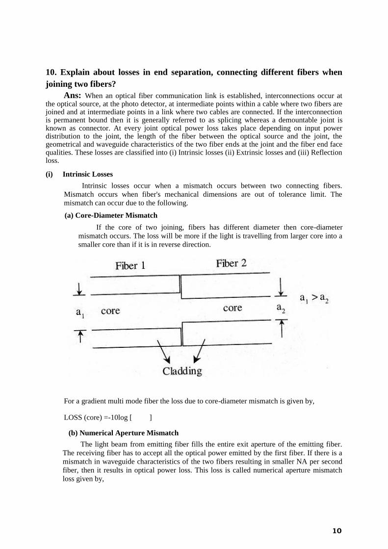
(a) Core-Diameter Mismatch
If the core of two joining, fibers has different diameter then core-diameter
mismatch occurs. The loss will be more if the light is travelling from larger core into a
smaller core than if it is in reverse direction.
For a gradient multi mode fiber the loss due to core-diameter mismatch is given by,
LOSS (core) =-10log [ ]
(b) Numerical Aperture Mismatch
The light beam from emitting fiber fills the entire exit aperture of the emitting fiber.
The receiving fiber has to accept all the optical power emitted by the first fiber. If there is a
mismatch in waveguide characteristics of the two fibers resulting in smaller NA per second
fiber, then it results in optical power loss. This loss is called numerical aperture mismatch
loss given by,
10

(c) Mode-Field-Diameter (MFD) Mismatch or Refractive Index Profile (α) Mismatch: This loss takes place only in graded-index fiber where the index profile emitting fiber is
different from the index profile of receiving fiber.
LOSSNA = -10log [ AA ]
The loss due to MFD is given by
LOSSMFD = ‐10log
Where α = index profile of fiber 1
α = index profile of fiber 2
11

(ii) Extrinsic Losses Extrinsic losses occur due to mechanical misalignment at point of joints. They are,
(a) Lateral Misalignment This misalignment occurs when the, fibers are displaced along the face of fiber and hence
the core overlapping area is reduced from circular to elliptical form hence power loss from
emitting fiber to the receiving is given below,
MMGI Fiber SM Fiber
Losslat = -10log 1 П Losslat = -10log
b) Angular Misalignment For a perfectly matched fiber, if point of joint at which core axis of fiber 1 is at an angle with
the core axis of fiber 2 then angular misalignment occurs and the result is same as due to
numerical aperture mismatch.
For MMG1 Fiber,
LOSSang = -10log 1 П
LOSSang = -log Where t = nПα0SM(θ)/λ
12
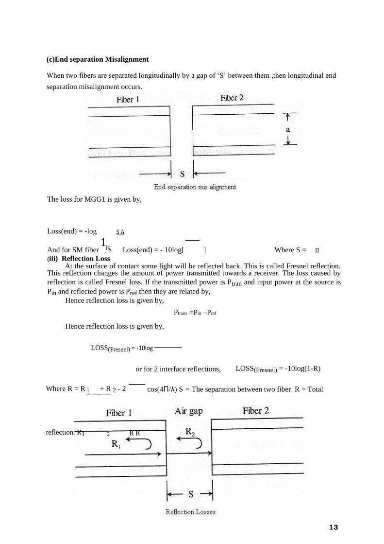
(c)End separation Misalignment When two fibers are separated longitudinally by a gap of ‘S’ between them ,then longitudinal end
separation misalignment occurs.
The loss for MGG1 is given by,
Loss(end) = -log
1is,
S A
П
And for SM fiber Loss(end) = - 10log[
] Where S =
(iii) Reflection Loss At the surface of contact some light will be reflected back. This is called Fresnel reflection.
This reflection changes the amount of power transmitted towards a receiver. The loss caused by
reflection is called Fresnel loss. If the transmitted power is Ptran and input power at the source is
Pin and reflected power is Pref then they are related by, Hence reflection loss is given by,
Ptrans =Pin –Pref
Hence reflection loss is given by,
LOSS(Fresnel) = ‐10log
or for 2 interface reflections, LOSS(Fresnel) = -10log(1-R)
Where R = R l + R 2 - 2
cos(4П/λ) S = The separation between two fiber. R = Total
reflection. R1
and R are reflections at two interfaces
2 R R
13

UNIT 4
1. What is splicing? Explain about fusion splicing?
Ans: Splicing A permanent joint formed between two individual optical fibers in the field is known as
splicing. The fiber splicing is used to establish optical fiber links, where smaller fiber lengths are
needed to be joined and where there is no requirement for repeated connection and disconnection.
Splicing can be divided into two broad categories depending on the splicing technique
utilized. These are fusion-splicing, mechanical or welding splicing. Fusion Splicing
Fusion splicing of single fibers involves the heating of the two prepared fiber ends to their
fusing point with sufficient axial pressure between the two optical fibers. It is essential that the
stripped fiber ends are adequately positioned and clamped with the aid of inspection microscope. The most widely used heating technique is an electric arc. This technique offers advantage
of consistent, easily controlled heat with adaptability for use under field conditions.
The welding of 2 fibers can be shown as illustrated in the following figure.
The figure shows basic arc fusion process, which involves the rounding of the fiber ends
with a low energy discharge before pressing the fibers together and fusing with a stronger arc. This technique is called perfusion. It removes the requirement for fiber end preparation. It
has been utilized with multimode fibers giving average splice losses of 0.09 dB.

Fusion splicing of single mode fibers with arc diameters between 5 and 10 um present
problems of more critical fiber alignment (lateral offsets of less than 1 um are required for low
loss joints). Splice uncertain losses below 0.3 dB may be achieved due to self alignment phenomenon
which partially compensates for any lateral offset. The drawback with fusion splicing is that the heat necessary to fuse the fibers may weaken the
fiber in the vicinity of the splice.
The tensile strength' of the fused fiber may be as low as 30% as that of the uncoated fiber before
fusion. The fiber fracture occurs in the heat affected zone adjacent to the fused joint. The reduced
tensile strength is attributed, to the combined effects of surface damage caused by handling,
surface defect growth during heating and induced stresses due to changes in chemical
composition. Hence it is necessary that splice is packaged so as to reduce tensile loading upon the
fiber in the vicinity of the splice.
2. Explain about adhesive splicing?
Ans:
Adhesive Splicing: A common method involves the use of ah accurately produced rigid
alignment tube into which the prepared fiber ends are permanently, bonded. This snug tube splice
may utilize a glass or ceramic capillary with an inner diameter just large enough to accept the
optical fibers. Transparent adhesive (e.g. epoxy resin) is injected through a transverse bore in die
capillary to give mechanical sealing and index matching of the splice. However, in general, snug
tube splices exhibit problems with capillary tolerance requirements.
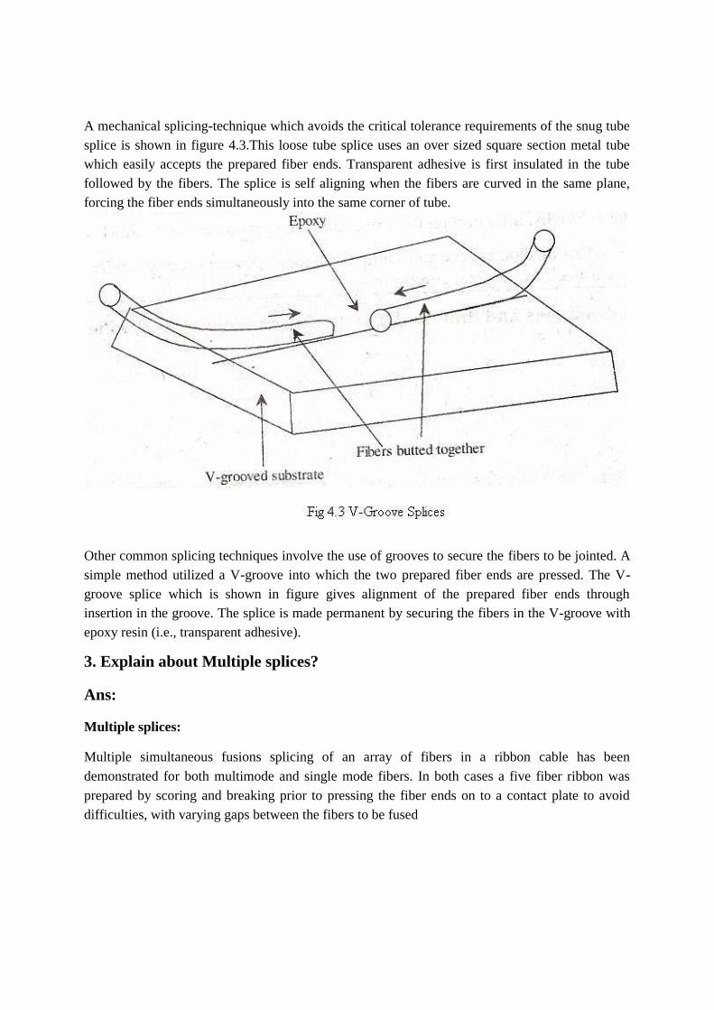
A mechanical splicing-technique which avoids the critical tolerance requirements of the snug tube
splice is shown in figure 4.3.This loose tube splice uses an over sized square section metal tube
which easily accepts the prepared fiber ends. Transparent adhesive is first insulated in the tube
followed by the fibers. The splice is self aligning when the fibers are curved in the same plane,
forcing the fiber ends simultaneously into the same corner of tube.
Other common splicing techniques involve the use of grooves to secure the fibers to be jointed. A
simple method utilized a V-groove into which the two prepared fiber ends are pressed. The V-
groove splice which is shown in figure gives alignment of the prepared fiber ends through
insertion in the groove. The splice is made permanent by securing the fibers in the V-groove with
epoxy resin (i.e., transparent adhesive).
3. Explain about Multiple splices?
Ans:
Multiple splices:
Multiple simultaneous fusions splicing of an array of fibers in a ribbon cable has been
demonstrated for both multimode and single mode fibers. In both cases a five fiber ribbon was
prepared by scoring and breaking prior to pressing the fiber ends on to a contact plate to avoid
difficulties, with varying gaps between the fibers to be fused
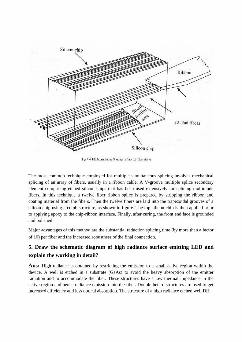
The most common technique employed for multiple simultaneous splicing involves mechanical
splicing of an array of fibers, usually in a ribbon cable. A V-groove multiple splice secondary
element comprising etched silicon chips that has been used extensively for splicing multimode
fibers. In this technique a twelve fiber ribbon splice is prepared by stripping the ribbon and
coating material from the fibers. Then the twelve fibers are laid into the trapezoidal grooves of a
silicon chip using a comb structure, as shown in figure. The top silicon chip is then applied prior
to applying epoxy to the chip-ribbon interface. Finally, after curing, the front end face is grounded
and polished
Major advantages of this method are the substantial reduction splicing time (by more than a factor
of 10) per fiber and the increased robustness of the final connection.
5. Draw the schematic diagram of high radiance surface emitting LED and
explain the working in detail?
Ans: High radiance is obtained by restricting the emission to a small active region within the
device. A well is etched in a substrate (GaAs) to avoid the heavy absorption of the emitter
radiation and to accommodate the fiber. These structures have a low thermal impedance in the
active region and hence radiance emission into the fiber. Double hetero structures are used to get
increased efficiency and less optical absorption. The structure of a high radiance etched well DH
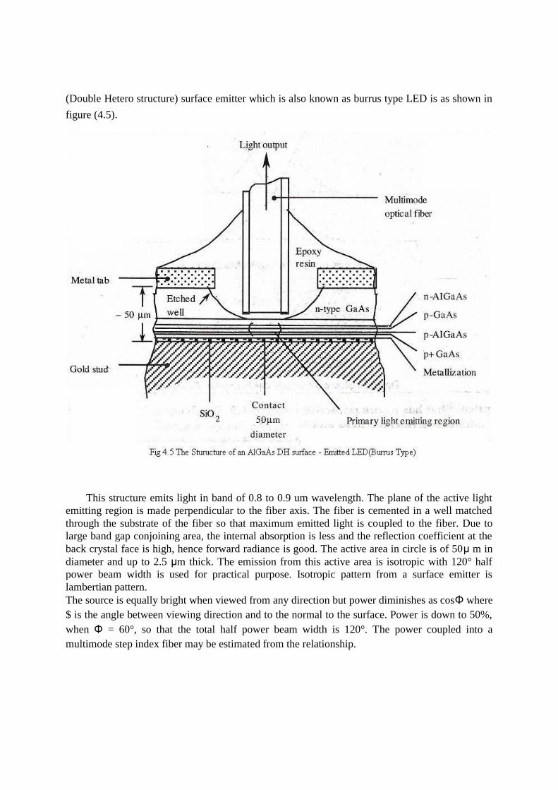
(Double Hetero structure) surface emitter which is also known as burrus type LED is as shown in
figure (4.5).
This structure emits light in band of 0.8 to 0.9 um wavelength. The plane of the active light
emitting region is made perpendicular to the fiber axis. The fiber is cemented in a well matched
through the substrate of the fiber so that maximum emitted light is coupled to the fiber. Due to
large band gap conjoining area, the internal absorption is less and the reflection coefficient at the
back crystal face is high, hence forward radiance is good. The active area in circle is of 50μ m in
diameter and up to 2.5 μm thick. The emission from this active area is isotropic with 120° half
power beam width is used for practical purpose. Isotropic pattern from a surface emitter is
lambertian pattern. The source is equally bright when viewed from any direction but power diminishes as cosΦ where
$ is the angle between viewing direction and to the normal to the surface. Power is down to 50%,
when Φ = 60°, so that the total half power beam width is 120°. The power coupled into a
multimode step index fiber may be estimated from the relationship.

PC =П(1-r)ARD (NA)2 ………..(1)
Where, PC = Power coupled into fiber
r = Fresnel reflection coefficient
A = Emission area of source
RD = Radiance of the source
NA = Numerical aperture
Power coupled into the fiber depends on (i) Distance and alignment between emission area and the fiber. (ii) Medium between the emitting area and the fiber. (iii) Emission pattern of SLED
Addition of Epoxy resin in the etched well reduces the refractive index mismatch and increases
the external power efficiency of the device. Hence the power coupled in the double hetero
structure surface emitters are more than Pc(optical power) that is given by equation (1), For graded
index fiber-direct coupling requires the source diameter of about one half the fiber core diameter
6. Draw the schematic of edge emitting double hetero junction LED and
explain its working in detail?
Ans: Double Hetero junction Laser
If a single p-n junction diode is fabricated from suitable single crystal semiconductor material it exhibits photo emissive properties. It is known as 'homo junction' p-n diode. However the emissive properties of a junction diode can be improved considerably by the use of 'hetero junction'. A hetero junction is an interface between two adjoining crystal semiconductors having different values of band gap energies. Devices are fabricated with hetero junction are said to have hetero structures.
They are of two types,
(i) Isotopes such as n-n or p-p type
(ii) Anisotope such as p-n type.
The isotope p-p junction has a potential barrier within the structure. The structure is capable of
confining min carriers to small active region called cavity. It effectively reduces the diffusion
length of the carrier and thus the volume of the structure where radioactive recombination may
occur.

Figures show the schematic layer structure, energy band diagram and refractive index
profile, for a double hetero junction injection laser diode with biasing. The laser oscillations take
place in the central p-type GaAs region which is known as active layer.
There is hetero junction at the both sides of the active layer. A forward bias voltage is applied by
connecting the positive electrode of the power supply voltage to the P-side of the structure and
negative electrode to the n-side when a voltage which is almost equal to the band gap energy. The
hetero junctions are used to provide potential barrier in the injection laser. In this structure it is
possible to obtain both carrier and optical containment to the active layer.

Broad Area Double Heterojunction Laser (DH Laser)
The above figure represents the layer structure of a broad area DH. The GaAs layers acts as active
layer which is sandwiched between p-type AZGaAs and n-A/GaAs layer and these two layers act
as the confinement layers. Light is emitted from the central GaAs active layer through the front
and back side of the device.
In the case of the DH broad area laser structure, the optical confinement in the vertical direction is
achieved by the refractive index at the hetero junction interfaces between the active layer and the
containment layers, but the laser .action takes places across the whole width of the device. In a
broad area laser the sides of the cavity are formed by simple roughening the ends of the device to
reduce the unwanted emission and limit the horizontal transverse modes.
Stripe Geometry Laser
In order to overcome the difficulties in a broad area laser structure, the stripe geometry laser
structure has developed and in this structure the active area does not enter upto the edges of the
device.
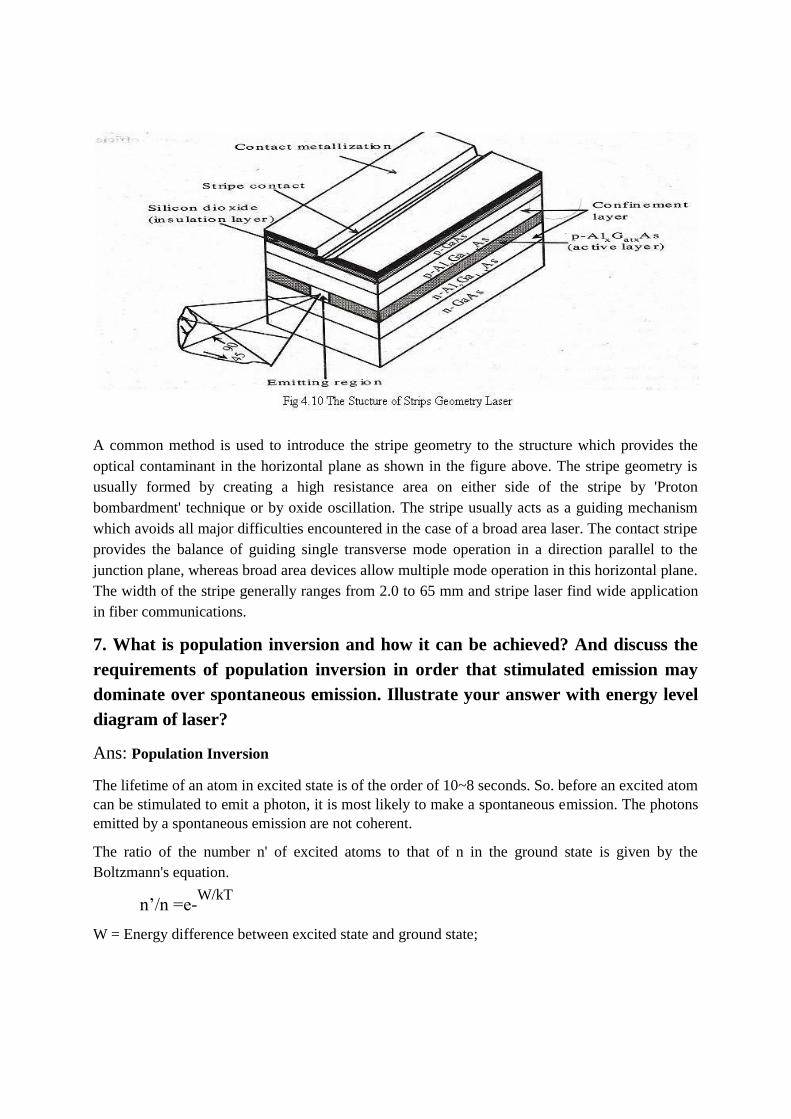
A common method is used to introduce the stripe geometry to the structure which provides the
optical contaminant in the horizontal plane as shown in the figure above. The stripe geometry is
usually formed by creating a high resistance area on either side of the stripe by 'Proton
bombardment' technique or by oxide oscillation. The stripe usually acts as a guiding mechanism
which avoids all major difficulties encountered in the case of a broad area laser. The contact stripe
provides the balance of guiding single transverse mode operation in a direction parallel to the
junction plane, whereas broad area devices allow multiple mode operation in this horizontal plane.
The width of the stripe generally ranges from 2.0 to 65 mm and stripe laser find wide application
in fiber communications.
7. What is population inversion and how it can be achieved? And discuss the
requirements of population inversion in order that stimulated emission may
dominate over spontaneous emission. Illustrate your answer with energy level
diagram of laser?
Ans: Population Inversion
The lifetime of an atom in excited state is of the order of 10~8 seconds. So. before an excited atom
can be stimulated to emit a photon, it is most likely to make a spontaneous emission. The photons
emitted by a spontaneous emission are not coherent.
The ratio of the number n' of excited atoms to that of n in the ground state is given by the
Boltzmann's equation.
n’/n =e-W/kT
W = Energy difference between excited state and ground state;

K = Boltzmann constant
T = Kelvin temperature.
Consider three level system in which three active energy levels E1 , E2 and E3 are present and
population in those energy levels are N, $1 and 7V3 respectively. In normal conditions E1< E2 <
E3 and N1 > N2 >N 3 E1 is the ground state, its lifetime is unlimited.E3 is highest energy state, its lifetime is very
less and it is the most unstable state. E. is in excited state and has more life time. Hence E2 is a meta stable state. When suitable form of energy is supplied to the system in a suitable way, then
the atoms excite from ground state (E1) to excited states (E2 and E3). Due to un stability, Excited
atoms will come back to ground state after the Life time of the respective energy states E2 and E3
If this process is continued then atoms will excite continuously to E2 and E3
Because E3 is the most unstable state, atoms will fall into E2 immediately. At some stage the
population in E2, will become more than the population in ground state. This situation is called
population inversion and is shown in figure 4.11
There are several ways of pumping a laser and producing population inversion necessary for
stimulated emission to occur. Most commonly used methods are as follows
There are several ways of pumping a laser and producing population inversion necessary for
stimulated emission to occur. Most commonly used methods are as follows.
1. Optical pumping
2. Electric discharge
3. Inelastic atom to atom collision
4. Direct conversion
5. Chemical reactions.
The emission process can occur in two ways
(i) Spontaneous Emission
The electrons in the excited state E2 are unstable. They return back to the lower energy
state without any external influence. This process leads to spontaneous emission.
(ii) Stimulated Emission When an external photon of energy which is equal to the energy difference between two
states (E2 – E1) hit the excited electron, this excited electron return to the ground state (E1) by
emitting a photon of energy hv12. This emission is known as stimulated emission.
Semiconductor laser diodes are preferred over LED for the optical fiber
communication systems requiring bandwidth greater than approximately 200 MHz.
Laser diodes have (i) Response time less than 1 ns (ii) Optical bandwidth of 2nm (iii) High coupling efficiency
For the efficient functioning of laser the method of exciting electrons in atoms is from,
1. Lower energy levels to higher energy levels.
2. Lower energy levels to large population inversion high energy level.
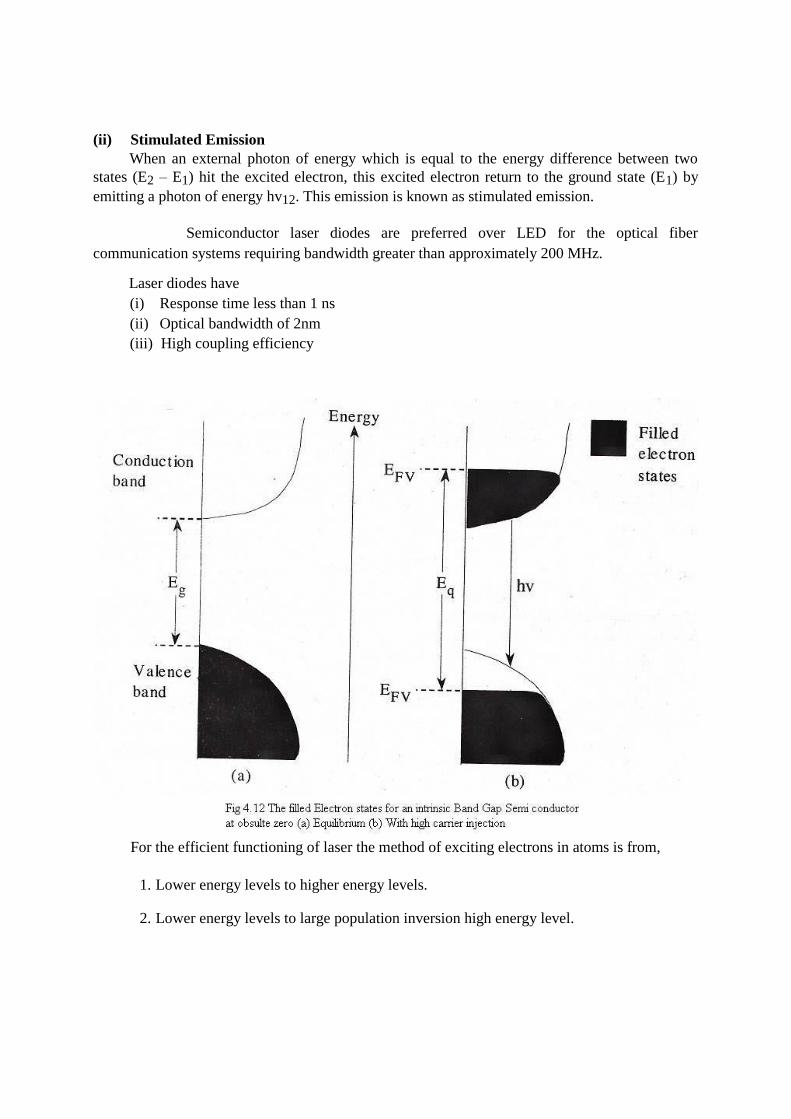
The stimulated emission in semiconductor laser arises from optical transitions between
distributions of energy state in the valence and conduction bands. Stimulated emission is achieved
in an intrinsic semiconductor by the injection of electrons into the material. Figure represents the
electron states for an intrinsic direct band gap semiconductor at absolute zero.
The population when the conduction band contains no electrons are injected into the material, fill
the lower energy states in the conduction band gap upto the injection energy or quasi fermi level
for electrons.
Since the charge is neutrally conserved with the material, an equal density of holes is created in
the top of the valence band by the absence of electrons as shown in the figure 1(b). Since more
electrons are there in valence band than the conduction band population inversion is achieved.
8. Obtain the expression for the 3dB modulation bandwidth of LED and
discuss the importance of radiative recombination life time?
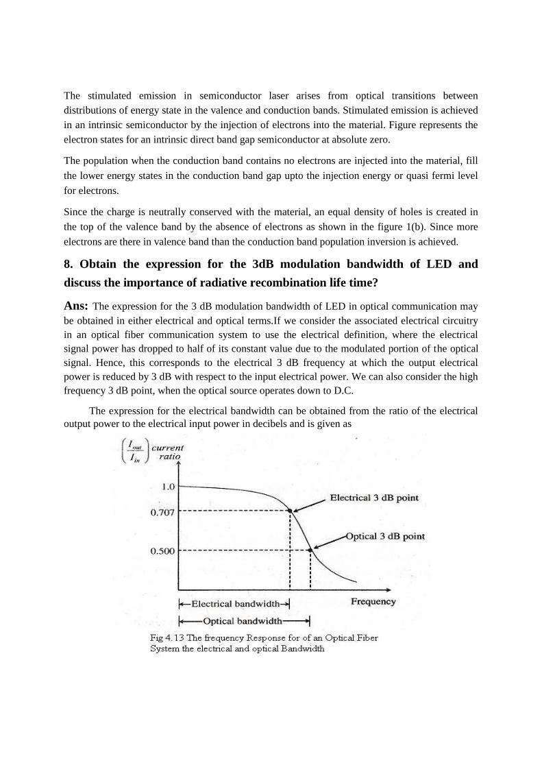
Ans: The expression for the 3 dB modulation bandwidth of LED in optical communication may
be obtained in either electrical and optical terms.If we consider the associated electrical circuitry
in an optical fiber communication system to use the electrical definition, where the electrical
signal power has dropped to half of its constant value due to the modulated portion of the optical
signal. Hence, this corresponds to the electrical 3 dB frequency at which the output electrical
power is reduced by 3 dB with respect to the input electrical power. We can also consider the high
frequency 3 dB point, when the optical source operates down to D.C.
The expression for the electrical bandwidth can be obtained from the ratio of the electrical
output power to the electrical input power in decibels and is given as

REdB = 10log10(Electrical output power /Electrical input power)
= 10log10
= 10 log10
The electrical 3 dB points occur when the ratio of electrical powers shown in above expression is
√2 Hence, it follows that this must Occur when,
/√2
Thus this expression depicts that the bandwidth of the electrical regime may be defined by the
frequency when the output current has dropped to /√2 (or) 0.707 of the input current of the
system.
Optical bandwidth can be obtained from the ratio of the optical power output to optical
power input in decibels ROdB is given by
ROdB = 10 log 10
= 10 log 10
Hence, the optical 3 dB points occur when the currents is equal to 0.5,hence .
Therefore In optical regime the bandwidth is defined by the frequency at which the output current
has dropped to 0.5 of the input current to the system.
The Modulation bandwidth of LED is generally determined by three methods ,They are
1. The doping level in the active layer, 2. Due to the injected carriers, the reduction in radiative lifetime.
3. The parasitic capacitance of the device.
If we assume that the parasitic capacitance is negligible, then the speed at which an LED can be
directly current modulated is fundamentally limited by the recombination lifetime of the carriers,

www.smartzworld.com www.jntuworldupdates.org
Optical Communications
1
Unit IV
P
P 1 ωτ
Where
P = Optical output power of the device
ω= Angular modulation frequency.
τ = Injected carrier lifetime in the recombination region
P D.C. optical output power for the same drive current
9. Discuss the major requirements of an optical source for use in optical
communication systems?
Ans: The development of efficient semiconductor optical sources along with low-loss optical fibers, led to substantial improvements in fiber optic communications. Semiconductor optical
sources have the physical characteristics and performance properties necessary for successful
implementations of fiber optic systems. It is desirable that optical sources must be, 1. Compatible in size to low-loss optical fibers by having a small light emitting which are capable
of launching light into fiber.
2. Launch sufficient optical power into the optical fiber to overcome fiber attenuation and
connection losses allowing for signal detection at the receiver.
3. Emit light at wavelengths that minimize optical fiber loss and dispersion.
4. Optical sources should have a narrow spectral width to minimize dispersion.
5. Allow for direct modulation of optical output power.
Maintain stable operation in changing environmental conditions (such as temperature).
Cost less and be more reliable than electrical devices, permitting fiber optic communication
systems to compete with conventional systems. Semiconductor optical sources suitable for fiber
optic systems range from inexpensive Light Emitting Diodes (LEDs) to more expensive
semiconductor lasers. Semiconductor LEDs and laser diodes are the principle light sources used
in fiber optics.
Semiconductor sources are designed to operate at wavelengths (i.e., 850 nm, 1300 nm and 1500
nm) that minimize optical fiber absorption and maximum system bandwidth. By designing an
optical source to operate at specific wavelengths, absorption from impurities in the optical fiber
such as hydroxyl ions (OH-) can be minimized. Maximizing system bandwidth involves

designing fibers and sources that minimize chromatic and inter modal dispersion at the intended
operational wavelength.
10. Compare the advantageous and disadvantageous of LED and Explain the
key process involved in the LASER operation?
Ans: 1. Simple Fabrication: There are no mirror facets and is some structures no striped geometry
2. Cost: The simpler construction of LED leas to much reduced cost which is always likely to be
maintained. 3. Reliability
The LED does not exhibit catastrophic degradation and has proved to be less sensitive to
gradual degradation than the injection laser. 4. Simpler Drive Circuitry
This is due to lower drive currents and reduced temperature dependance which makes
temperature compensation circuits unnecessary. 5. Linearity
Ideally, the LED has a linear light output against current characteristics unlike the injection laser. Disadvantage An LED radiates rather dispersed light, which makes coupling this light into an optical fiber a
problem.
The key processes involved in laser action are as given below. (i) Absorption. (ii) Spontaneous emission. (iii) Stimulated emission.
These three key processes are represented by 2-energy level diagrams.
Where, E1 = Energy of ground state.
E2 = Energy of excited state.
(i) Absorption
When transition occurs between two states, then it involves the emission and absorption of
energy in the form of photon energy hvn = E2 – E 1

In the above figure we can see that electron in 'E1’ absorbs the photon energy and is excited to
state lE2' when photon of energy hvn is incident on the system.
(ii) Spontaneous Emission
Charge carriers are unstable in excited state so they try to come back in stable state and this
is possible by emission of radiation. This emission takes place when energy hvv is released. As it occurs without any external stimulation, it is known as spontaneous emission. (iii) Stimulated Emission
Here in this type of emission when a photon of energy hv12 is striking on system while the
electron is still in its excited state, then the electron is stimulated so that it drops on to ground state
and gives a photon of energy hvn and the emitted photon will be in phase with incident photon.
The resultant emission is called as stimulated emission.

UNIT 5
1.Briefly explain about source output pattern in power launching from source
to fiber.
Ans:
Source Output Pattern
Consider the following figure 5.1.1, which shows a spherical coordinate system
characterized by R, θ and φ with the normal to the emitting surface being the polar axis. The
radiance may be a function of both θ and φ, and can also vary from point to point on the emitting
surface. Surface emitting LEDs are characterized by their lambertian output pattern, which
means the source is equally bright when viewed from any direction. The power delivered at an
angle 'θ', measured relative to a normal to the emitting surface, varies as cos θ because the
projected area of the emitting surface varies as cos θ with viewing direction. The emission
pattern for a lambertian source thus follows the relationship.
B(θ,φ) =B0 cos θ
Figure 5.1.2, shows the radiation pattern for a lambertian source. The complexity of
emission pattern is still increases, when we consider edge-emitting LEDs and laser diodes. In the
planes parallel and normal to the emitting junction plane of the device. The radiances of these
devices are given by, B(θ, 0°) and B(θ, 90°). Generally, these radiances can be approximated as,
,
Where,
T = Transverse power distribution coefficient
L = Lateral power distribution coefficient.
For edge emitter L=1 and T is significantly large value.
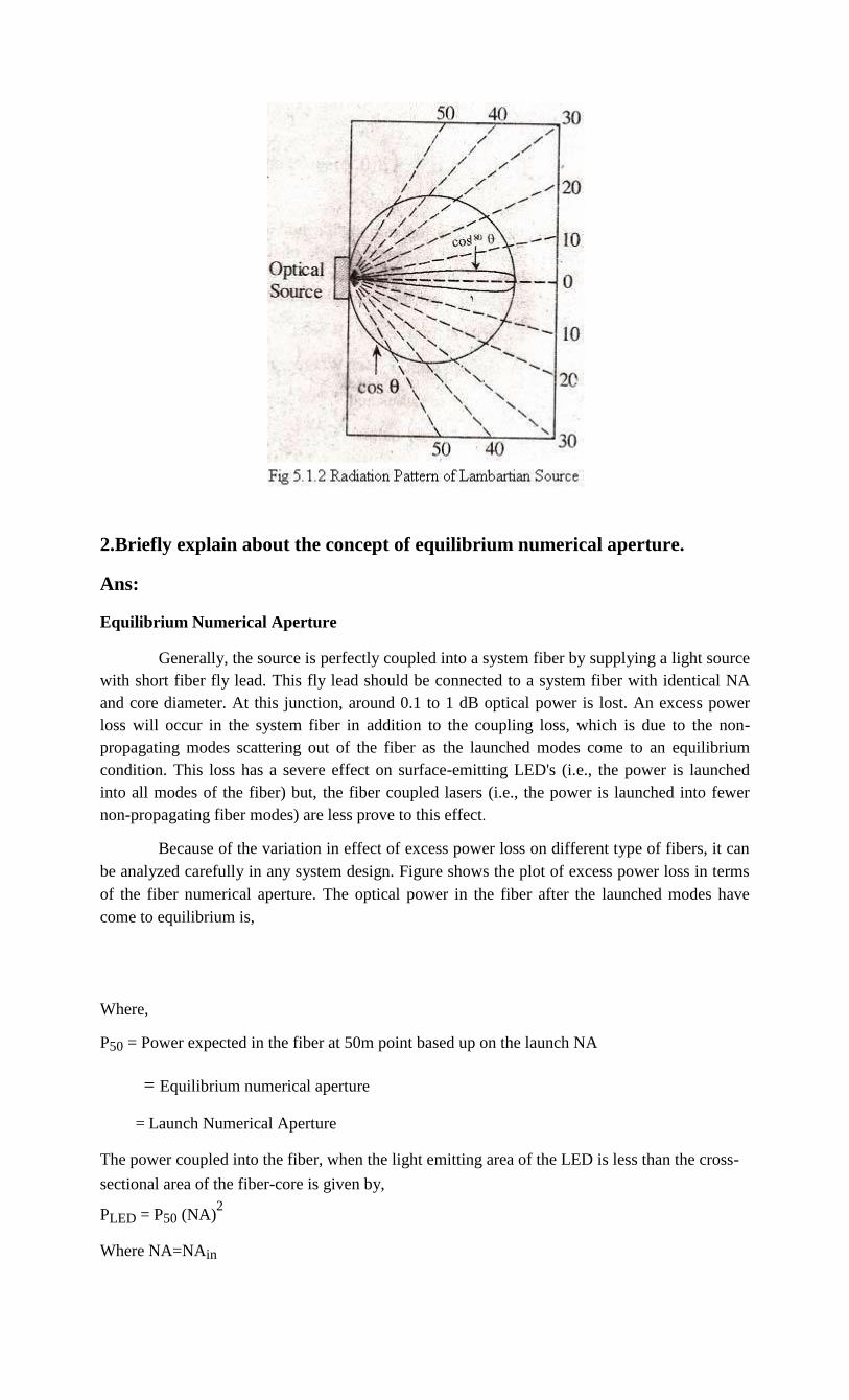
2.Briefly explain about the concept of equilibrium numerical aperture.
Ans: Equilibrium Numerical Aperture
Generally, the source is perfectly coupled into a system fiber by supplying a light source
with short fiber fly lead. This fly lead should be connected to a system fiber with identical NA
and core diameter. At this junction, around 0.1 to 1 dB optical power is lost. An excess power
loss will occur in the system fiber in addition to the coupling loss, which is due to the non-
propagating modes scattering out of the fiber as the launched modes come to an equilibrium
condition. This loss has a severe effect on surface-emitting LED's (i.e., the power is launched
into all modes of the fiber) but, the fiber coupled lasers (i.e., the power is launched into fewer
non-propagating fiber modes) are less prove to this effect.
Because of the variation in effect of excess power loss on different type of fibers, it can
be analyzed carefully in any system design. Figure shows the plot of excess power loss in terms
of the fiber numerical aperture. The optical power in the fiber after the launched modes have
come to equilibrium is, Where,
P50 = Power expected in the fiber at 50m point based up on the launch NA
= Equilibrium numerical aperture
= Launch Numerical Aperture The power coupled into the fiber, when the light emitting area of the LED is less than the cross-
sectional area of the fiber-core is given by,
PLED = P50 (NA)2
Where NA=NAin
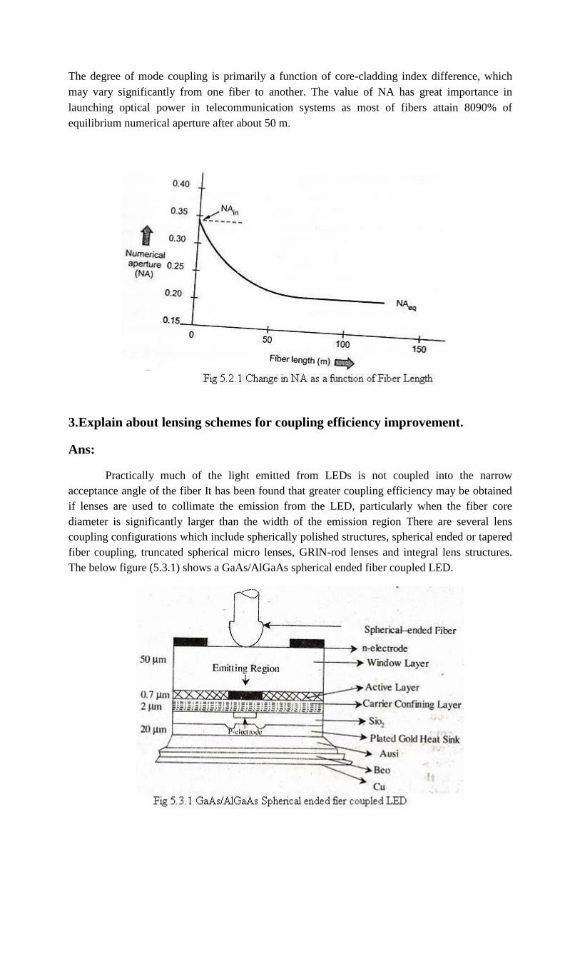
The degree of mode coupling is primarily a function of core-cladding index difference, which
may vary significantly from one fiber to another. The value of NA has great importance in
launching optical power in telecommunication systems as most of fibers attain 8090% of
equilibrium numerical aperture after about 50 m.
3.Explain about lensing schemes for coupling efficiency improvement.
Ans:
Practically much of the light emitted from LEDs is not coupled into the narrow
acceptance angle of the fiber It has been found that greater coupling efficiency may be obtained
if lenses are used to collimate the emission from the LED, particularly when the fiber core
diameter is significantly larger than the width of the emission region There are several lens
coupling configurations which include spherically polished structures, spherical ended or tapered
fiber coupling, truncated spherical micro lenses, GRIN-rod lenses and integral lens structures.
The below figure (5.3.1) shows a GaAs/AlGaAs spherical ended fiber coupled LED.

It consists of a planar surface emitting structure with the spherical ended fiber attached to
the cap by epoxy resin. An emitting diameter of 35 μm is fabricated into the device and light is
coupled into fibers with core diameters or 75 μm and 110 μm. For increased coupling efficiency
it is necessary that the active diameter of the device be substantially less than the fiber core
diameter by a factor of 2. In this case a coupling efficiency of 6% is obtained. Another lens
coupling technique employs a truncated spherical micro lens. This is shown in figure (5.3.2).
Efficient coupling is obtained when diameter of emission region is much smaller than the
core diameter of the fiber. In this case the best results are obtained with a 14 μm active diameter
and an 85 μm core diameter step index fiber with a numerical aperture of 0.16. The coupling
efficiency was increased by a factor of 13. The integral lens structure has a useful power
coupling strategy for use with surface emitters. In this technique a low absorption lens is formed
at the exit face of the substrate material instead of it being fabricated in glass and attached to a
planar sLED with Epoxy. This method provides an advantage that the semiconductor epoxy lens
interface is eliminated which can limit the maximum lens gain of sLEDs. Lens coupling can also
be usefully employed with edge emitting devices. Practically lens attached to the fiber ends or
tapered fiber lenses are widely used to increase coupling efficiency.
4.Explain about laser diode-to-fiber
coupling. Ans:
We know that the edge emitting laser diodes have the emission pattern that nominally has
a Full-Width at Half-Maximum (FWHM) of 30° - 50° in the perpendicular plane to the active
area junction and an FWHM of 5° to 10° in the parallel plane to the junction. Since the fiber
acceptance angle is smaller than the angular output distribution of the laser and since the fiber
core is much greater than the laser emitted area, spherical (or) cylindrical lenses (or) optical fiber
tapers can also be used to improve the coupling efficiency between edge emitting laser diodes
and optical fibers. This phenomenon also works well for Vertical Cavity Surface Emitting Lasers
(VCSELs). Here the outcome 35% of coupling efficiencies to multimode fibers for mass-
produced connections of laser arrays to parallel optical fibers are possible by direct coupling
from a single Vertical Cavity Surface Emitting Lasers (VCSELs) source to a multimode fiber.

The measured FWHM value of the laser output beams are,
1.For near field parallel to junction lies between 3 and 9 urn.
2.For field perpendicular to the junction lies between 30° and
60°. 3.For field parallel to the junction lies between 15° and 55°.
In practice, the coupling efficiencies ranges between 50% and 80%.
5. Differentiate between Lambertian and monochromatic optical sources in
terms of power coupling into a single mode fiber.
Ans: Lambertian optical sources emits equal brightness when viewed from any direction.
Surface emitting LED's exhibit Lambertian output pattern. The power delivered at an angle G,
measured with respect to a line drawn perpendicular to emitting surface varies as a function
of'cost)'. The Lambertian source emission pattern is given as,
B(θ,Φ) = B0cosθ
Where,
B0 – Radiation along θ=00 i.e., perpendicular line from emitting surface.
The monochromatic optical sources has a narrow output beam in a particular direction i.e., high
directivity is exhibited by monochromatic sources. Laser's exhibit monochromatic pattern.
Because of high directivity, the monochromatic sources couples more power into single mode
fibers than Lambertian sources. The patterns for Lambertian and monochromatic sources are shown in the following figure.
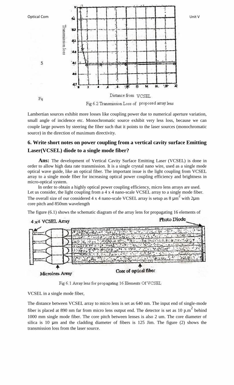
Optical Com Unit V Lambertian sources exhibit more losses like coupling power due to numerical aperture variation,
small angle of incidence etc. Monochromatic source exhibit very less loss, because we can
couple large powers by steering the fiber such that it points to the laser sources (monochromatic
source) in the direction of maximum directivity.
6. Write short notes on power coupling from a vertical cavity surface Emitting
Laser(VCSEL) diode to a single mode fiber?
Ans: The development of Vertical Cavity Surface Emitting Laser (VCSEL) is done in order to allow high data rate transmission. It is a single crystal nano wire, used as a single mode
optical wave guide, like an optical fiber. The important issue is the light coupling from VCSEL
array to a single mode fiber for increasing optical power coupling efficiency and brightness in
micro-optical system. In order to obtain a highly optical power coupling efficiency, micro lens arrays are used.
Let us consider, the light coupling from a 4 x 4 nano-scale VCSEL array to a single mode fiber.
The overall size of our considered 4 x 4 nano-scale VCSEL array is setup as 8 μm2 with 2μm
core pitch and 850nm wavelength The figure (6.1) shows the schematic diagram of the array lens for propagating 16 elements of
VCSEL in a single mode fiber, The distance between VCSEL array to micro lens is set as 640 nm. The input end of single-mode
fiber is placed at 890 nm far from micro lens output end. The detector is set as 10 p.m2 behind
1000 mm single mode fiber. The core pitch between lenses is also 2 um. The core diameter of
silica is 10 μm and the cladding diameter of fibers is 125 Jim. The figure (2) shows the
transmission loss from the laser source.

The transmission loss is 1.9 dB at 1000 mm far from VCSEL array. The spot size of laser
source is 360 nm. But here, the spot size is 2000 nm at 500 mm far from the VCSEL array, and the spot size is still below 2000 nm at 1000 mm far from the VCSEL array. Therefore, using the array lens, we can increase the irradiation field distribution of VCSEL array in a single-mode fiber.
Figure (6.3) shows the irradiance distribution and pattern of the 4 x 4 VCSEL array light
output after propagating 1000 mm long of single-mode fiber through 4 x 4 micro lens array.
array using 4 x 4 BK7 micro lens array, we can simultaneously convey each laser beam,
from 360 nm to 2000 nm into a 1000 mm long single mode fiber.

7. List the factors involved in launching optical power from a light source to a
optical fiber?
Ans: Source To Fiber power Launching: Launching optical power from source into fiber needs te following considerations: (i) Numerical Aperture (ii) Core Size (iii) Refractive index profile (iv) Core cladding index difference to the
fiber (v) Radiance (vi) Angular power distribution of the optical source ' A measure of the amount of optical power emitted from a source that can be coupled into a fiber
usually given by the coupling efficiency is defined as
PF/PS
Where PF is the power coupled into the fiber and Ps is the power emitted from the light source. The launching or coupling efficiency depends on the type of fiber that is attached to the
source and on the coupling process, many source suppliers offer devices with short length of optical fiber (lm or less) attached in an optimum power configuration.
This section of fiber is generally referred to as fly lead devices. These fly lead sources reduces
many power-launching problems and make the coupling easier. The effects to e considered are: (i) Fiber misalignment (ii) Different core sizes (iii) Numerical apertures (iv) Core refractive index
(V ) The need for clean and smooth fiber end faces that are perpendicular to the fiber axis.
While considering the source to fiber power coupling efficiency, the radiance (spatial
distribution of optical power) is important rather than the total output power.
8.For an optical source having refractive index of 3.6 coupled to a fiber of 1.48
refractive index. Considering the medium between fiber and source has
similar index as that of fiber. Calculate Fresnel reflection and loss of power in
dBs. Ans: Given data,
Source refractive index, n1 = 3.6
Fiber refractive index, n = 1.48 Fresnel reflection R =
R =
. . . .
R = 0.1741
Power loss L = -10 log (1-R)
L = -10 log (1-0.1741) L = 0.83 dB.


UNIT 6
1. With schematic representation explain the working principle of pin photo
diode. Ans: PIN Photodiode
PIN diode consists of an intrinsic semiconductor sandwiched between two heavily
doped p-type and n-type semiconductors as shown in Fig. 6.1.1. Sufficient reverse voltage is
applied so as to keep intrinsic region free from carriers, so its resistance is high, most of diode
voltage appears across it, and the electrical forces are strong within it. The incident photons give
up their energy and excite an electron from valance to conduction band. Thus a free electron hole
pair is generated, these are called as photo carriers. These carriers are collected across the reverse
biased junction resulting in rise in current in external circuit called photocurrent.
In the absence of light, PIN photodiodes behave electrically just like an ordinary rectifier
diode. If forward biased, they conduct large amount of current. PIN detectors can be operated in
two modes, Photovoltaic and photoconductive. In photovoltaic mode, no bias is applied to the
detector. In this case the detector works very slow, and output is approximately logarithmic to the
input light level. Real world fiber optic receivers never use the photovoltaic mode. In
photoconductive mode, the detector is reverse biased. The output in this case is a current that is
very linear with the input light power. The intrinsic region somewhat improves the sensitivity of
the device. It does not provide internal gain. The combination of different semiconductors
operating at different wavelengths allows the selection of material capable of responding to the
desired operating wavelength.
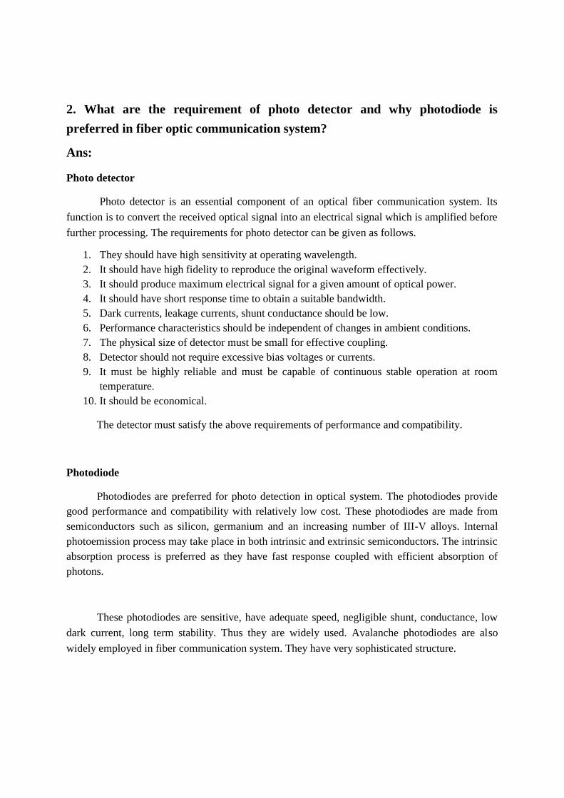
2. What are the requirement of photo detector and why photodiode is
preferred in fiber optic communication system? Ans: Photo detector
Photo detector is an essential component of an optical fiber communication system. Its
function is to convert the received optical signal into an electrical signal which is amplified before
further processing. The requirements for photo detector can be given as follows.
1. They should have high sensitivity at operating wavelength. 2. It should have high fidelity to reproduce the original waveform effectively. 3. It should produce maximum electrical signal for a given amount of optical power. 4. It should have short response time to obtain a suitable bandwidth. 5. Dark currents, leakage currents, shunt conductance should be low. 6. Performance characteristics should be independent of changes in ambient conditions. 7. The physical size of detector must be small for effective coupling. 8. Detector should not require excessive bias voltages or currents. 9. It must be highly reliable and must be capable of continuous stable operation at room
temperature. 10. It should be economical.
The detector must satisfy the above requirements of performance and compatibility.
Photodiode
Photodiodes are preferred for photo detection in optical system. The photodiodes provide
good performance and compatibility with relatively low cost. These photodiodes are made from
semiconductors such as silicon, germanium and an increasing number of III-V alloys. Internal
photoemission process may take place in both intrinsic and extrinsic semiconductors. The intrinsic
absorption process is preferred as they have fast response coupled with efficient absorption of
photons.
These photodiodes are sensitive, have adequate speed, negligible shunt, conductance, low
dark current, long term stability. Thus they are widely used. Avalanche photodiodes are also
widely employed in fiber communication system. They have very sophisticated structure.

3. With schematic representation explain the working principle of Avalanche
Photodiode. Ans: Avalanche Photodiode
When a p-n junction diode is applied with high reverse bias breakdown can occur by two
separate mechanisms direct ionization of the lattice atoms, zener breakdown and high velocity
carriers causing impact ionization of the lattice atoms called avalanche breakdown. APDs use the
avalanche breakdown phenomena for its operation. The APD has its internal gain which increases
its responsivity. Fig. 6.3.1 shows the schematic structure of an APD. By virtue of the doping
concentration and physical construction of the n+ p junction, the electric field is high enough to
cause impact ionization. Under normal operating bias, the I-layer (the p~ region) is completely
depleted. This is known as reach through condition, hence APDs are also known as reach through
APD or RAPDs.
Similar to PIN photodiode, light absorption in APDs is most efficient in I-layer. In this
region, the E-field separates the carriers and the electrons drift into the avalanche region where
carrier multiplication occurs. If the APD is biased close to breakdown, it will result in reverse
leakage current. Thus APDs are usually biased just below breakdown, with the bias voltage being
tightly controlled. The multiplication for all carriers generated in the photodiode is given as
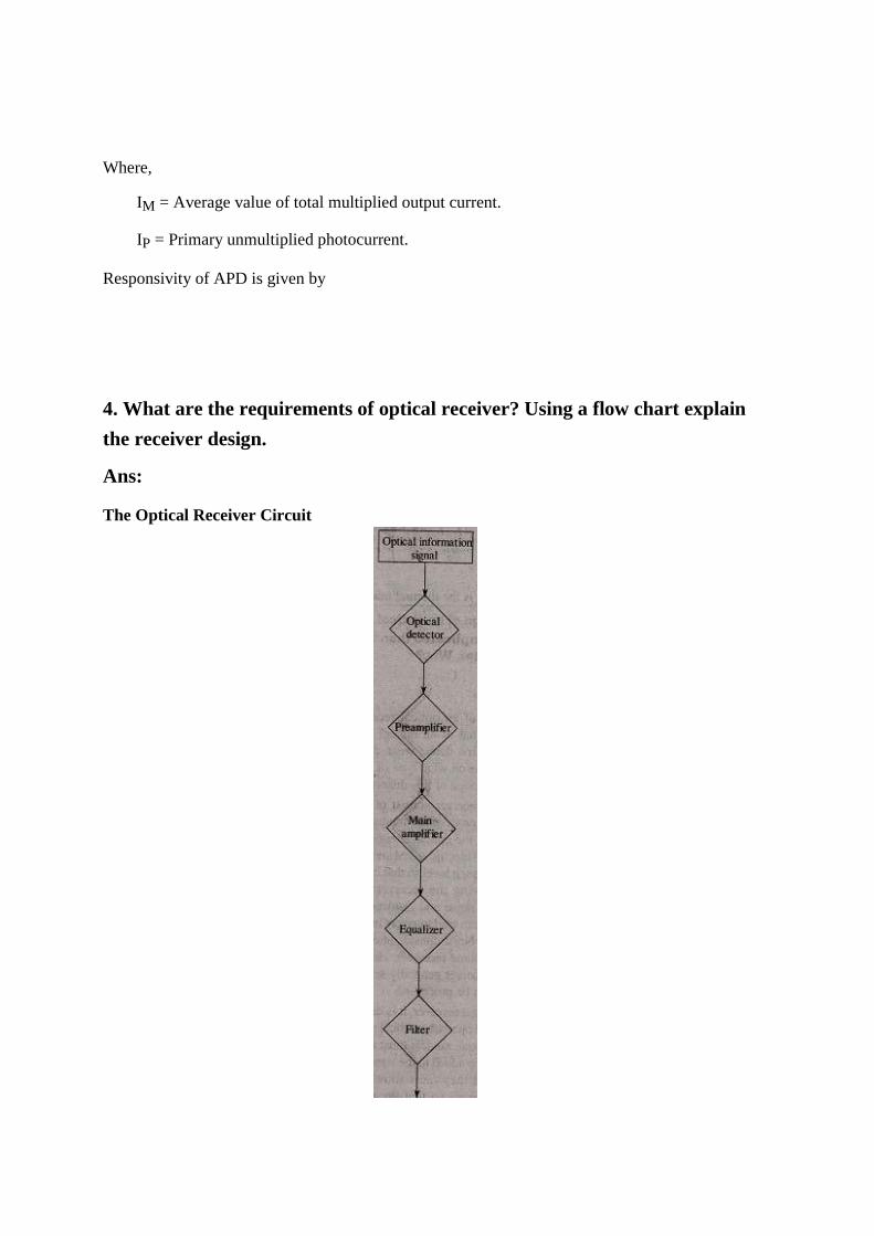
Where,
IM = Average value of total multiplied output current.
IP = Primary unmultiplied photocurrent. Responsivity of APD is given by
4. What are the requirements of optical receiver? Using a flow chart explain
the receiver design.
Ans: The Optical Receiver Circuit

A flow chart depicting the receiver design is shown above. The optical signal received is
linearly converted into an electrical signal at the detector, it is amplified to obtain a suitable signal
level. Initially the amplification is performed in the preamplifier circuit, where it is important that
the additional noise is kept to a minimum in order to avoid corruption of the received signal.
As the noise source within the preamplifier may be dominant, its configuration and
design are major factors in determining receiver sensitivity. The main amplifier provides
additional low noise amplification of the signal to give an increased signal level for the following
circuits. Even though the optical detectors are linear devices and do not provide any distortion.
Other components in the system may exhibit nonlinear behavior to remove this i.e., to compensate
for the distortion, equalizers are used. The function of the filter is to maximize the acquired signal
to noise ratio without destroying the essential features of the signal.
5. Explain various errors that occur in the detection mechanism.
Ans:
Errors in detection mechanism can arise from various noises and disturbances
associated with the signal detection system, as shown in figure. The term noise is used customarily
to describe unwanted components of an electric signal that tend to disturb the transmission and
processing of the signal in a physical system, and over which we have incomplete control. The
noise sources can be either external to the system or internal to the system. The two most common
noises are shot noise and thermal noise. Shot noise arises in electronic devices since of the discrete
nature of current flow in the device. Thermal noise arises from the random motion of electrons in
a conductor. The random arrival rate of signal photons produces a quantum or shot noise at the
photo detector. Since this noise depends on the signal
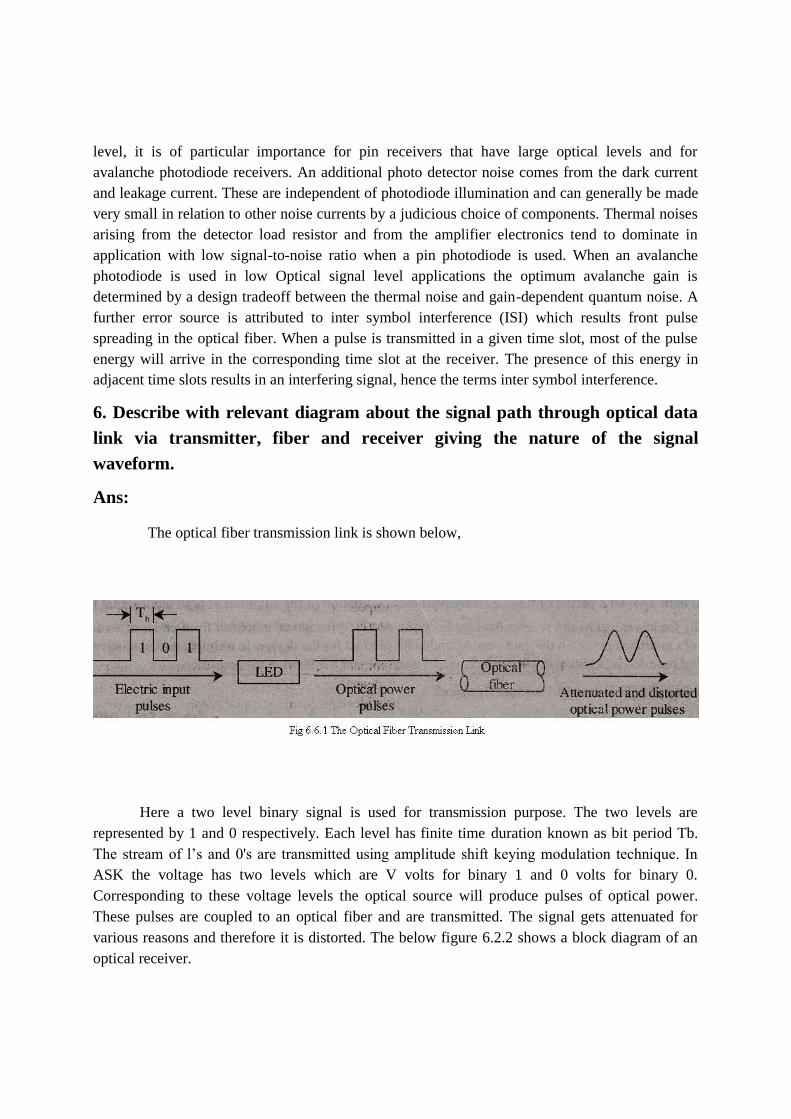
level, it is of particular importance for pin receivers that have large optical levels and for
avalanche photodiode receivers. An additional photo detector noise comes from the dark current
and leakage current. These are independent of photodiode illumination and can generally be made
very small in relation to other noise currents by a judicious choice of components. Thermal noises
arising from the detector load resistor and from the amplifier electronics tend to dominate in
application with low signal-to-noise ratio when a pin photodiode is used. When an avalanche
photodiode is used in low Optical signal level applications the optimum avalanche gain is
determined by a design tradeoff between the thermal noise and gain-dependent quantum noise. A
further error source is attributed to inter symbol interference (ISI) which results front pulse
spreading in the optical fiber. When a pulse is transmitted in a given time slot, most of the pulse
energy will arrive in the corresponding time slot at the receiver. The presence of this energy in
adjacent time slots results in an interfering signal, hence the terms inter symbol interference.
6. Describe with relevant diagram about the signal path through optical data
link via transmitter, fiber and receiver giving the nature of the signal
waveform.
Ans:
The optical fiber transmission link is shown below,
Here a two level binary signal is used for transmission purpose. The two levels are
represented by 1 and 0 respectively. Each level has finite time duration known as bit period Tb.
The stream of l’s and 0's are transmitted using amplitude shift keying modulation technique. In
ASK the voltage has two levels which are V volts for binary 1 and 0 volts for binary 0.
Corresponding to these voltage levels the optical source will produce pulses of optical power.
These pulses are coupled to an optical fiber and are transmitted. The signal gets attenuated for
various reasons and therefore it is distorted. The below figure 6.2.2 shows a block diagram of an
optical receiver.

At the receiver the distorted signal is coupled to a photo detector generally a pin diode
which produces an electric current which is equivalent to the incoming signal. The amplifier and
filter removes noise and amplifies the signal. The decision making device gives output binary 1
for a voltage V and 0 for a voltage 0 respectively. At the signal processing circuiting the signal is
demodulated thus producing the desired output.
7. Describe important specifications of semiconductor photo diode to be
suitable for fiber optic communications.
Ans: Specifications of a Semiconductor Photo Diode
The important performance parameters of a semiconductor photodiode are described below. 1. Responsivity
The ratio of generated photocurrent to incident light power, typically expressed in A/W
when used in photo conductive mode. The responsivity may also be expressed as quantum
efficiency or the ratio of the number of photo generated carriers to incident photons and thus, a
unit less quantity. The typical values for responsivity are, 0.65 for A/W silicon at 900 nm, 0.45
A/W for germanium at 1.3 μm and 0.9 A/W for InGaAs at 1.3 μm. 2. Dark Current
The current through the photodiode in the absence of light, when it is operated in
photoconductive m dark current includes photocurrent generated by background radiation and

the saturation current of the semiconductor junction. Dark current must be accounted for calibration if a photodiode is used to make an accurate optical measurement. It is also a source of
noise when a photo diode is used in an optical communication system. 3. Noise Equivalent Power (NEP)
The minimum input optical power to generate photocurrent, equal to the r.m.s noise
current in a 1 Hz bandwidth. The related characteristic directivity D IS the inverse of NEP i.e.,
1/NEP and the specific directivity D* is the directivity normalized to the area, A of the photodiode
i.e., √
4. Quantum Efficiency
The photodiode's capability to convert light energy to electrical energy is referred as quantum efficiency, it can be also described as the ratio of number of electron-hole pairs generated to the number of incident photons. In a practical photodiode, the quantum efficiency of the detector ranges from 30 to 95%. 5. Sensitivity
It is a measure of the effectiveness of a detector in producing an electrical signal at the
peak sensitivity wavelength. 6. Rise time
The time required for a detector output to reach from 10 to 90% of its final value.
8. With the help of a suitable block diagram explain the functioning of every
element of a fiber optic receiver. Ans: Fiber Optic Receiver
The terra receiver at the output end of the fiber optic cable refers to both a light
detecting transducer and its related electronics, which provides any necessary signal conditioning
to restore the signal to its original shape at the input, as well as additional signal amplification. To
interface the receiver with the optical fiber, the proper match between light source, fiber optic
cable and light detector is required. In the AM transmission system, the optical power input at the
fiber is modulated so that the photo detector operating in the photocurrent mode must provide
good linearity, speed and stability.
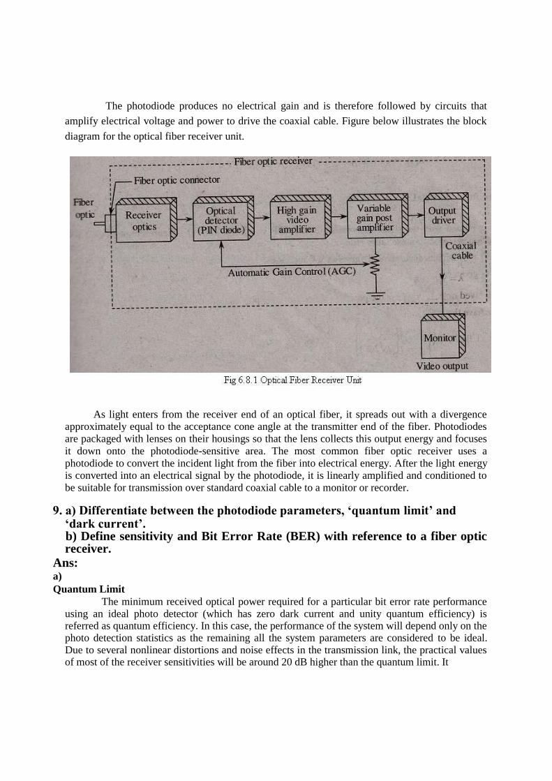
The photodiode produces no electrical gain and is therefore followed by circuits that
amplify electrical voltage and power to drive the coaxial cable. Figure below illustrates the block
diagram for the optical fiber receiver unit.
As light enters from the receiver end of an optical fiber, it spreads out with a divergence approximately equal to the acceptance cone angle at the transmitter end of the fiber. Photodiodes
are packaged with lenses on their housings so that the lens collects this output energy and focuses
it down onto the photodiode-sensitive area. The most common fiber optic receiver uses a
photodiode to convert the incident light from the fiber into electrical energy. After the light energy is converted into an electrical signal by the photodiode, it is linearly amplified and conditioned to
be suitable for transmission over standard coaxial cable to a monitor or recorder.
9. a) Differentiate between the photodiode parameters, ‘quantum limit’ and ‘dark current’. b) Define sensitivity and Bit Error Rate (BER) with reference to a fiber optic receiver.
Ans: a) Quantum Limit
The minimum received optical power required for a particular bit error rate performance using an ideal photo detector (which has zero dark current and unity quantum efficiency) is referred as quantum efficiency. In this case, the performance of the system will depend only on the photo detection statistics as the remaining all the system parameters are considered to be ideal. Due to several nonlinear distortions and noise effects in the transmission link, the practical values of most of the receiver sensitivities will be around 20 dB higher than the quantum limit. It
is also very important to differentiate average power and peak power while specifying he quantum
limit. Dark Current
In the absence of light, the current that flows continuously through the basic circuit of the device is referred as dark current or the leakage current that flows when the photodiode is in the dark and a reverse voltage is applied across the junction is referred as dark current. This voltage may be low as 10 mV or as high as 50 V and the dark current may vary from pA to uA depending on the junction area and the process used.
The dark current is temperature dependent. The rule of thumb is that the dark
current will approximately double for every 10°C increase in ambient temperature. However,
specific diode types can vary considerably from this relationship. b)
Sensitivity
The sensitivity of the receiver is defined as the minimum amount of optical power required to achieve a specific receiver performance. The receiver takes many signals such as synchronous
signals (to recover the clock signal similar to that is used at transmitter), decoded data and errors.
So, in order to generate a correct signal in the presence of all these signals, a receiver should have high sensitivity. If it has high sensitivity it will be even able to detect low level optical signals.
Thus, the higher the sensitivity, the more efficiently the receivers can detect the attenuated on low level signals. The sensitivity of receiver can be sketched taking the data rate and optical power that the receiver can detect.
Bit Error Rate (BER)
In practice, that there are several standard ways of measuring the rate of error occurrences in
a digital data stream. One common approach is to divide the number Ne of errors occurring over a
certain time interval t by number Nt of pulses (ones and zeros) transmitted during this interval. This is called either the error rate of the bit error rate, which is commonly abbreviated as BER. Thus, we have
BER = Ne/Nt 10. A pin photodiode on average generates one electron hole pair per three
incident photons at a wavelength of 0.8 μ m. Assuming all the electrons are collected, calculate
i) The quantum efficiency of the device ii) Its maximum possible band gap energy
iii) The mean output photocurrent when the received optical power is 10-7
W.
Ans Given that,
For a pin photodiode one electron hole pair generated for every three incident photons.
Operating wavelength, λ = 0.8 μm

i) Quantum efficiency of the device, = ?
ii) Maximum possible band gap energy, Eg = ? iii) Received optical power, P0 = 10
-7 W
iv) Mean output photocurrent, Ip = ?
i) Quantum efficiency of the device is given by,
N
100
100
100 0.3333 100 33.33
33.33%
ii) The maximum possible band gap energy is given by, /
. . . 2.486 10
. 1.552
iii) The mean output photo current is given by,
. 21.46
.
Ip = 21.46 nA

UNIT 7
1. Discuss about the choice of different components in designing an optical
fiber link. Discuss the shortcomings of decency of each component. Ans:
The system designer has many choices when selecting components for an optical fiber
system. The major components choices are,
(i) Optical Fiber Type and Parameters Multimode or single mode, size, refractive index, attenuation, dispersion,
mode coupling, strength, joints etc.
(ii) Source Type
Laser or LED, optical power launched into the fiber, rise and fall time,
stability etc.,
(iii) Transmitter Configuration
Design for digital or analog, input impedance, supply voltage, dynamic
range, feedback etc.
(iv) Detector Type and Characteristics
p-n, p-i-n or avalanche photodiode, response time, active diameter, bias
voltage, dark current etc.
(v) Receiver Configuration
Preamplifier design, BER, SNR, range etc.
(vi) Modulation and Coding Source intensity modulation, pulse frequency modulation, PWM and PPM
transmission.
(vii) Digital transmission or analog transmission such as biphase scheme and FM
respectively. These decisions will be taken depending on the system performance,
ready availability of suitable components and cost.
The shortcomings of the components can be mentioned as follows,
(i) LED may appear ideally suitable for analog transmission most of the LED display
some degree of non-linearity in their output.
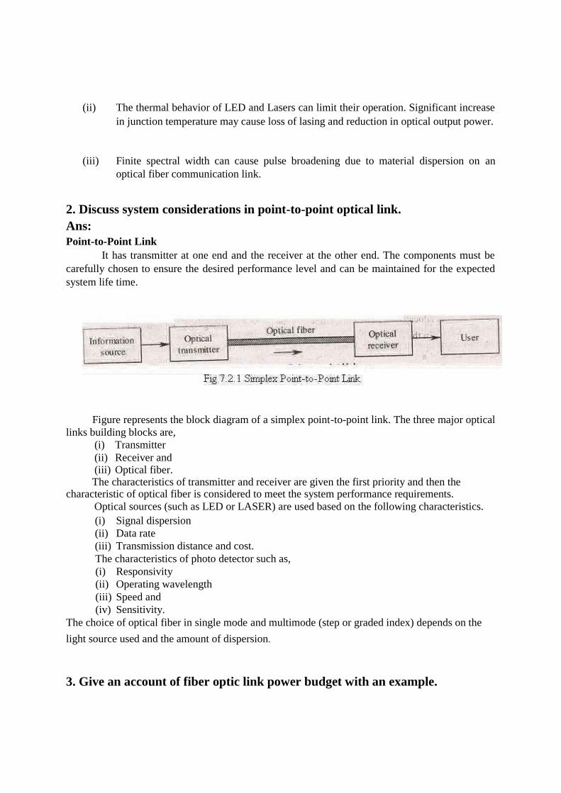
(ii) The thermal behavior of LED and Lasers can limit their operation. Significant increase
in junction temperature may cause loss of lasing and reduction in optical output power.
(iii) Finite spectral width can cause pulse broadening due to material dispersion on an
optical fiber communication link.
2. Discuss system considerations in point-to-point optical link.
Ans: Point-to-Point Link
It has transmitter at one end and the receiver at the other end. The components must be
carefully chosen to ensure the desired performance level and can be maintained for the expected
system life time.
Figure represents the block diagram of a simplex point-to-point link. The three major optical
links building blocks are, (i) Transmitter (ii) Receiver and (iii) Optical fiber. The characteristics of transmitter and receiver are given the first priority and then the
characteristic of optical fiber is considered to meet the system performance requirements. Optical sources (such as LED or LASER) are used based on the following characteristics. (i) Signal dispersion (ii) Data rate (iii) Transmission distance and cost. The characteristics of photo detector such as, (i) Responsivity (ii) Operating wavelength (iii) Speed and (iv) Sensitivity.
The choice of optical fiber in single mode and multimode (step or graded index) depends on the
light source used and the amount of dispersion.
3. Give an account of fiber optic link power budget with an example.
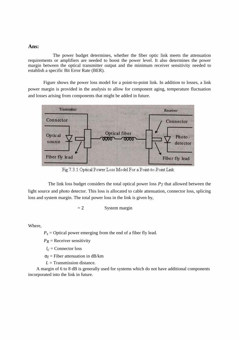
Ans:
The power budget determines, whether the fiber optic link meets the attenuation requirements or amplifiers are needed to boost the power level. It also determines the power margin between the optical transmitter output and the minimum receiver sensitivity needed to establish a specific Bit Error Rate (BER).
Figure shows the power loss model for a point-to-point link. In addition to losses, a link
power margin is provided in the analysis to allow for component aging, temperature fluctuation
and losses arising from components that might be added in future.
The link loss budget considers the total optical power loss PT that allowed between the
light source and photo detector. This loss is allocated to cable attenuation, connector loss, splicing
loss and system margin. The total power loss in the link is given by,
= 2 System margin Where,
Ps = Optical power emerging from the end of a fiber fly lead.
PR = Receiver sensitivity
lc = Connector loss
αf = Fiber attenuation in dB/km
L = Transmission distance. A margin of 6 to 8 dB is generally used for systems which do not have additional components
incorporated into the link in future.

4. Write short notes on system considerations in the design of a fiber optic link.
Ans:
The design of an optical fiber link involves many considerations regarding the fiber, source and photo detector operation and performance characteristics. Expected life time with performance and cost constrains were considered while designing a fiber link. The system considerations are choosing the transmitting wave length and components that operates in this region. The wavelength range 800-900 nm is chosen for shorter distances and 1300-1550 nm for longer distances with low attenuation and dispersion.
Next, we consider receiver, transmitter and implement them on a fiber to check whether the desired performance characteristics are obtainable or not. We first select a photo detector. In doing so, we should determine the minimum detectable optical power in order to satisfy Bit Error Rate at specified data rate. Cost and complexity are also considered here. The systems considerations with cheap and less complex one is preferred. P-i-n diodes are used as they are simple, high temperature tolerance, less bias voltages. APD's are used to detect low power levels which are not done by P-i-n.
Next, we choose the transmitting elements. While choosing LED or laser, we should consider data rate, dispersion, cost, and transmission distances. Laser provides the advantage of longer repeater less transmission distance and low dispersion. LED's offer low cost and simpler circuitry.
Next we have to choose an optical fiber that may be single mode or multimode with step or graded index core. The choice is made depending on dispersion tolerance and type of source. Edge emitting LED's along with single mode fiber launches sufficient power and support transmission data rates >500 Mbps. LED's can be used with multimode fibers.
While choosing attenuation characteristics of fiber, we should consider cabling process loss,
and fiber attenuation, connector loss, splice loss and losses due to atmospheric conditions also. After considering a system satisfying above conditions, the "Link power Budget" and "Rise time
budget" techniques are used to ensure the desired performance characteristics are met or not.
5. List the estimates and conclusions possible from transmission distance
versus bit rate plot for the given wavelength LED-PIN diode combination.
Ans:
The plot of transmission distance Vs the bit rate for a short wavelength (800-900 nm)
LED-PIN diode combination is shown in figure 7.5.1.

The above plot shows the limitation of attenuation and dispersion on transmission
distance as a function of data rate. The Bit Error Rate (BER) is considered to be 10-9
for all the
cases. The fiber-coupled LED output power is taken as -13 dBm for all data rates up to 200 Mbps.
The attenuation limit curve is drawn by taking a fiber loss of 3.5 dB/km. We include 1 dB
connector coupling loss at both ends and a system margin 6 dB. We consider material dispersion
to be 3.5 ns/km with 50 nm spectral width. From figure 7.5.1 it is clear that a data rate of 40 Mbps
over which the transmission distance is attenuation limited and below which the transmission
distance is material dispersion limited. Suppose, take a data rate of 200 Mbps, the attenuation is 3 km x 3.5 dB/km = 10.5 dB and
dispersion is, 2 km x 3.5 ns = 7 ns, the transmission distance is just 2 km. Now, consider a data
rate of 2 Mbps, the attenuation is 10 km x 3.5 dB/km = 35 dB and dispersion is almost '0'. The
transmission distance is 10 kms. From the above two estimations we conclude that higher data rates can be transmitted to a smaller
distance with less attenuation and high dispersion while, lower data rates (2 Mbps) can be
transmitted up to a larger distance of 10 km with high attenuation and no dispersion. If we choose
an optimum data rate of 20 Mbps, the attenuation and dispersion are high and can be used for
optimum transmission distance.
6. Discuss the difference between dispersion limited and an attenuation limited
fiber optic link. Ans:
Dispersion Limited Fiber Optic Link Attenuation Limited Fiber Optic Link
1. When the data rates are higher than 40 Mbps, 1. When the data rates are lower than 40 Mpbs,
the transmission distance is limited by dispersion the transmission distance is limited by attenuation
parameter. parameter.
2. In this, there is no effect of attenuation losses. 2. In this, there is no effect of dispersion.
3. In this, losses are occurred due to increase 3. In this, losses are produced due to the
pulse width, which in turn results in overlapping absorption by fiber, material imperfections, and
with neighboring pulses. fiber bents.
4. The attenuation limit curve has a negative slope
4. This limit is taken at a distance at which
because the minimum optical power at receiver
tmat is 70% of a bit duration. increases with increasing data rates at a constant
BER.
5. Rise time budget analysis is a good method for 5. Link power budget is a convenient method to
calculating the dispersion limitation of an calculate attenuation limitation of an optical fiber
optical fiber link. link.

7. Describe the procedure to determine the maximum allowed NRZ or RZ data
rate on a given fiber optic link. Ans:
The procedure which is followed to determine the maximum allowed NRZ or RZ data
rate on a given fiber optic link is described below.
1. Initially, calculate the source rise time (rrs), inter modal dispersion rise time (tmod), intra modal
pulse broadening rise time (rmat) and detector rise time (rrd) by using given data.
2. Then, calculate the total system rise time (tsys ) using below formula as,
⁄
3. In the rise time calculations involving optical fiber systems, the constant 0.35is often utilized.
Hence, 0.35
Where,
τ = Pulse duration. 4. For an RZ pulse format, the bit rate B = 1/τ and the expression for maximum allowed RZ data
rate of a given fiber optic link is given by, .
5. For NRZ pulse format, the BT = B/2 = (1/2τ) and the expression for maximum allowed NRZ
data rate of given fiber optic link is given by, .
6. In a RZ pulse format, the upper limit on tsys should be less than 35% of the bit interval. In a
NRZ pulse format, the upper limit on tsys should be less than 70% of the bit interval.
8. Discuss the effect of mode mixing factor on modal dispersion for calculating
the maximum allowable transmission data rate in a fiber optic link. Ans:
Information is carried by light in an optical fiber, which is injected into
optical fiber cable by optical Source in the form of many individual modes. These individual
modes do not travel throughout the fiber instead, they transfer large energy to their adjacent
modes. This type of mode conversion is known as mode coupling or mode mixing. This mode mixing factor affects the propagation characteristics in many ways, the major one is related to
dispersive properties of fibers.
The sensitivity of the receiver reduces due to pulse broadening (by dispersion) caused due to finite bandwidth. This leads to increase in bit error rate and Inter Symbol Interference (ISI). Equalization phenomenon compensates above loss at receiver. This is known as dispersion-
equalization or ISI penalty (DL ).
dB, given by Gaussian pulses.
Te = 1/e full width pulse broadening due to dispersion.
T = Bit period.
But, for Gaussian pulses.
Te = 2 √2
2 2 √2
Where,
BT = Bit rate
σ = r.m.s pulse width.
Pulse broadening is caused due to intermodal and/or intramodal dispersion. Multimode fibers
exhibit considerable intermodal (modal) dispersion. We know pulse broadening (Intermodal) is
proportional directly to length 'L' of fiber.
The presence of mode coupling (or) mixing along with intermodal dispersion slows the rate
at which pulse broadening increases with length 'L'.
At lower bit rates, the effect of mode mixing on the dispersion-equalization penalty is
almost negligible. At higher bit rates, mode mixing factor controls the dispersion-equalization
penalty, in fact it reduces the penalty. It-also increases the repeater spacing. Hence, maximum
allowable bit-rate is obtained by providing desired bandwidth. In order to obtain desired
bandwidth, the pulse broadening should be reduced. As the mode coupling factor reduces the
dispersion equalization penalty, pulse broadening (due to modal dispersion) is also reduced. Thus,
maximum allowable bit rate is attained using mode mixing effect on modal dispersion.
9. The rise times for various components of intensity modulated fiber optic link
are listed below. Determine if these specifications support a 5 km repeater less
fiber optic link with 6 MHz optical bandwidth.
Rise time of LED transmitter electronics = 10 ns
Inter-modal dispersion induced = 8ns/km
Intra-modal dispersion induced = 2ns/km
Rise time of Detector and receiver electronics = 3ns
Ans:
Given that,
Optical bandwidth = 6 Mhz
Length of the fiber optic link = 5 km
trise = 10 ns
tinter = 8 ns/km
tinter = 5 x 8 ns = 40 ns for 5
km tintra = 2 ns/km = 10 ns for
5 km tr = 3 ns
Now,
10 10 40 10 10 10 3 10 42.5
We know that maximum rise time of system is, . 58.6
42.5 58.6
Hence, the given specifications give a system rise time that satisfies the bandwidth requirement
of optical fiber. Hence, these support a repeater less communication.
10. (i) What is essential to initiate a system design?
(ii) Explain briefly about multiplexing.
Ans: (i)
To initiate a system design certain basic system requirements must be specified.
These specifications includes, 1. Type of transmission i.e., digital or analog. 2. System fidelity. For a digital system, it is specified in terms of BER and for an analog
system it is specified in terms of received SNR and signal distortion. 3. Bandwidth required for transmission. 4. Spacing between the terminal equipment or intermediate repeaters. 5. Cost. 6. Reliability. (ii)
The transfer of information over an optical fiber communication link can be increased by multiplexing several signals on to a single fiber. These multichannel signals are carried by multiplexing in time or frequency domain, prior to intensity modulation of optical source.
The technique of separating signals in time is called Time Division Multiplexing (TDM). Narrow pulses from multiple modulators under the control of a common clock (commutator) are fed to a single channel. Pulses from individual channels are interleaved and transmitted sequentially, thus enhancing the bandwidth utilization of a single fiber link. The technique of separating signals in frequency is called Frequency Division Multiplexing
(FDM). In FDM, the optical channel bandwidth is divided into a number of non-overlapping
frequency bands and each signal is assigned one of these bands of frequencies. The individual
signals can be extracted from the combined FDM signal by appropriate electrical filtering at the
receiving terminal. In contrast to the FDM, it is possible to utilize a number of optical sources
each operating at a different wavelength on the single fiber link. In this technique, referred to as
Wavelength Division Multiplexing (WDM), the separation and extraction of the multiplexed
signals (i.e., wavelength separation) is performed with optical filters.
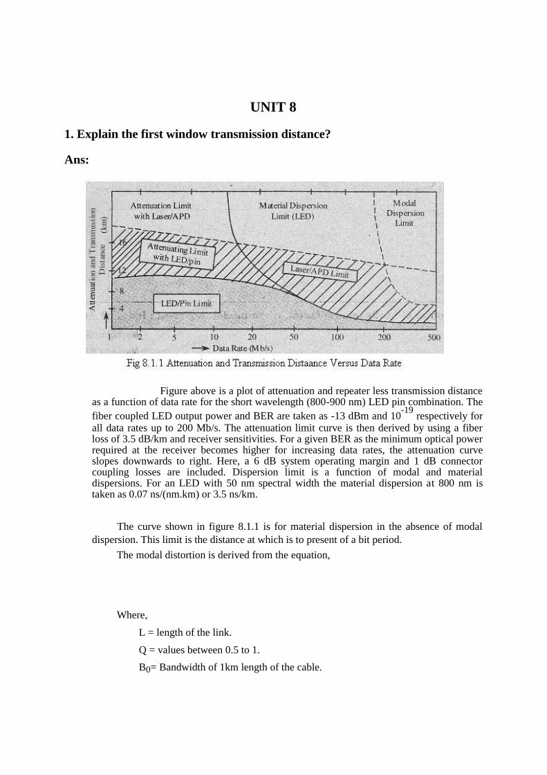
UNIT 8
1. Explain the first window transmission distance?
Ans:
Figure above is a plot of attenuation and repeater less transmission distance
as a function of data rate for the short wavelength (800-900 nm) LED pin combination. The
fiber coupled LED output power and BER are taken as -13 dBm and 10-19
respectively for all data rates up to 200 Mb/s. The attenuation limit curve is then derived by using a fiber loss of 3.5 dB/km and receiver sensitivities. For a given BER as the minimum optical power required at the receiver becomes higher for increasing data rates, the attenuation curve slopes downwards to right. Here, a 6 dB system operating margin and 1 dB connector coupling losses are included. Dispersion limit is a function of modal and material dispersions. For an LED with 50 nm spectral width the material dispersion at 800 nm is taken as 0.07 ns/(nm.km) or 3.5 ns/km.
The curve shown in figure 8.1.1 is for material dispersion in the absence of modal
dispersion. This limit is the distance at which is to present of a bit period.
The modal distortion is derived from the equation,
Where,
L = length of the link.
Q = values between 0.5 to 1.
B0= Bandwidth of 1km length of the cable.
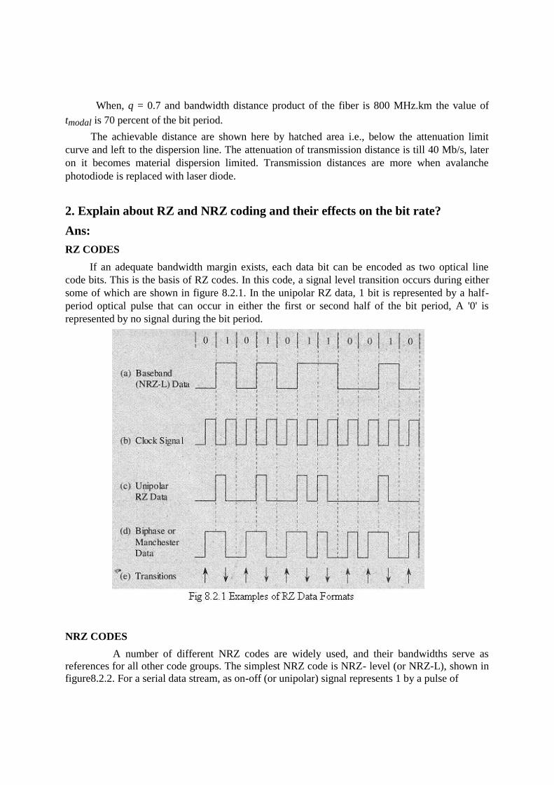
When, q = 0.7 and bandwidth distance product of the fiber is 800 MHz.km the value of
tmodal is 70 percent of the bit period.
The achievable distance are shown here by hatched area i.e., below the attenuation limit
curve and left to the dispersion line. The attenuation of transmission distance is till 40 Mb/s, later
on it becomes material dispersion limited. Transmission distances are more when avalanche
photodiode is replaced with laser diode.
2. Explain about RZ and NRZ coding and their effects on the bit rate?
Ans: RZ CODES
If an adequate bandwidth margin exists, each data bit can be encoded as two optical line
code bits. This is the basis of RZ codes. In this code, a signal level transition occurs during either
some of which are shown in figure 8.2.1. In the unipolar RZ data, 1 bit is represented by a half-
period optical pulse that can occur in either the first or second half of the bit period, A '0' is
represented by no signal during the bit period.
NRZ CODES
A number of different NRZ codes are widely used, and their bandwidths serve as
references for all other code groups. The simplest NRZ code is NRZ- level (or NRZ-L), shown in
figure8.2.2. For a serial data stream, as on-off (or unipolar) signal represents 1 by a pulse of

current or light filling an entire bit period, whereas for a 0 no pulse transmitted. These codes are
simple to generate & decode, but they possess no inherent error-monitoring or correcting capabilities and they have no self-clocking (timing) features.
A disadvantage of the unipolar RZ format is that long strings of 0 bits can cause loss of timing
synchronization. A common data format not having this limitation is the biphase or optical
Manchester code. Note that this is a unipolar code, which is in contrast to the conventional bipolar
Manchester code used in wire lines. The optical Manchester signal is obtained by direct modulo-2
addition of the-baseband (NRZ-L) signal and a clock signal. In this code, there is a transition at
the centre of each bit interval. A negative-going transition indicates a 1 bit whereas a positive-
going transition means a 0 bit was sent. Since it is an RZ-type code, it requires twice the
bandwidth of an NRZ code. In addition, it has no inherent error-detecting or correcting capability.
3. What are the underlying principles of the WDM technique? What are its various advantages? How is it different from FDM technique? Ans: Wavelength Division Multiplexing (WDM)
FDM stands for Frequency Division Multiplexing. In this scheme the numbers of different
frequencies are combined together and pass through low pass filling in order to remove unwanted
interferences and an adder, which combines frequencies at the output. At the demultiplexer the
individual frequency signals can be obtained by means of a decoder. FDM provides high
frequency range in order to associate n number of users. This system provides high capacity. This
system is almost in all communications. An interesting and powerful aspect of an optical
communication link is that many different wavelengths can be sent along a fiber simultaneously in
1300 to 1600 nm spectrum.
This is achieved through WDM (Wavelength Division Multiplexing). Combining a
number of wavelengths on a same fiber is known as WDM. 'N' independent optically formatted
information streams, each transmitted at a different wavelength are combined with optical
multiplexer and sent over the same fiber as shown in figure 8.3.1.

Each of the streams could be a different data rate. Each information stream maintains its
individual data rate after being multiplexed with other streams and operates at its unique
wavelength. The basic of WDM has to use multiple sources operating at slightly different
wavelengths to transmit and WDM must be properly spaced to avoid inter channel interference.
Features of Wavelength Division Multiplexing
1. Capacity Upgrade The classical application of WDM is to upgrade the capacity of existing point-to-
point fiber optic transmission links. If each wavelength supports an independent network
signal of a few gigabits per second, then WDM can increase the capacity of a fiber
network dramatically. 2. Transparency
An important aspect of WDM is that each optical channel can carry any
transmission format. 3. Wavelength Routing
In addition to the usage of multiple wavelengths to increase link capacity and
flexibility, the use of wavelength-sensitive optical routing devices, in designing
communication meteorology and switches has a very important role. Wavelength routed
networks use the final address. 4. Wavelength switching
Wavelength routed networks are based on a rigid fiber structure, wavelength
switched architectures allow reconfigurations of the optical layer.
Operation Principle of WDM
The key feature of WDM is that the discrete wavelengths form an orthogonal set of
carriers that can be separated, routed and switched without interfering with each other as shown in
figure 8.3.2.
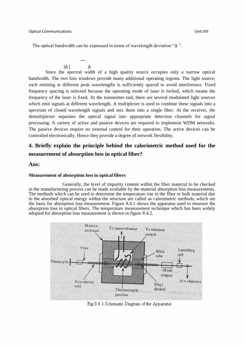
Optical Communications Unit VIII
The optical bandwidth can be expressed in terms of wavelength deviation “∆ ”.
|∆ |
∆
Since the spectral width of a high quality source occupies only a narrow optical
bandwidth. The two loss windows provide many additional operating regions. The light source,
each emitting at different peak wavelengths is sufficiently spaced to avoid interference. Fixed
frequency spacing is selected because the operating mode of laser is locked, which means the
frequency of the laser is fixed. At the transmitter end, there are several modulated light sources
which emit signals at different wavelength. A multiplexer is used to combine these signals into a
spectrum of closed wavelength signals and mix them into a single fiber. At the receiver, the
demultiplexer separates the optical signal into appropriate detection channels for signal
processing. A variety of active and passive devices are required to implement WDM networks.
The passive devices require no external control for their operation. The active devices can be
controlled electronically. Hence they provide a degree of network flexibility.
4. Briefly explain the principle behind the calorimetric method used for the
measurement of absorption loss in optical fiber? Ans: Measurement of absorption loss in optical fibers
Generally, the level of impurity content within the fiber material to be checked in the manufacturing process can be made available by the material absorption loss measurements. The methods which can be used to determine the temperature rise in the fiber or bulk material due to the absorbed optical energy within the structure are called as calorimetric methods, which are the basis for absorption loss measurement. Figure 8.4.1 shows the apparatus used to measure the absorption loss in optical fibers. The temperature measurement technique which has been widely adopted for absorption loss measurement is shown in figure 8.4.2.
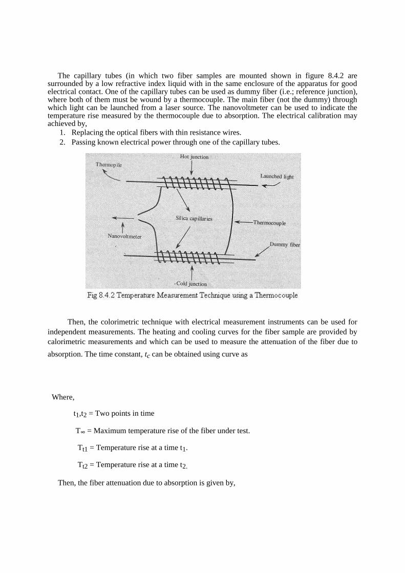
The capillary tubes (in which two fiber samples are mounted shown in figure 8.4.2 are surrounded by a low refractive index liquid with in the same enclosure of the apparatus for good electrical contact. One of the capillary tubes can be used as dummy fiber (i.e.; reference junction), where both of them must be wound by a thermocouple. The main fiber (not the dummy) through which light can be launched from a laser source. The nanovoltmeter can be used to indicate the temperature rise measured by the thermocouple due to absorption. The electrical calibration may achieved by,
1. Replacing the optical fibers with thin resistance wires. 2. Passing known electrical power through one of the capillary tubes.
Then, the colorimetric technique with electrical measurement instruments can be used for
independent measurements. The heating and cooling curves for the fiber sample are provided by
calorimetric measurements and which can be used to measure the attenuation of the fiber due to
absorption. The time constant, tc can be obtained using curve as
Where,
t1,t2 = Two points in time
T∞ = Maximum temperature rise of the fiber under test.
Tt1 = Temperature rise at a time t1.
Tt2 = Temperature rise at a time t2.
Then, the fiber attenuation due to absorption is given by,

Where, C = Constant proportional to the thermal capacity per unit length of silica capillary and
the low refractive index liquid surrounding the fiber.
Popt = Optical power propagation in the fiber under test.
5. Describe with suitable diagram, for measurement of fiber attenuation using
cutback technique? Ans: Experimental setup for Cutback Technique
Cutback technique is the common technique used for the measurement of fiber
attenuation. In this technique, the white focused light is mechanically chopped [cut into pieces] at
a low frequency [say 200Hz] which enables lock-in amplifier to perform a phase-sensitive
detection. Then the light is passed through a monochromator which uses a prism to select the
required wavelength for the measurement of attenuation.
After filtering the light, it is focused onto the fiber by means of a
microscopic objective lens. A beam splitter is used before the fiber to provide light for vision and
a reference signal is used compensate for output power fluctuations (changes). A mode scrambler
is also attached to fiber within the first meter. Fiber is passed through S-shaped groove cut in the
Teflon in a cladding mode stripper device through which radiation removes light launched into the
fiber and then sends to index matched-glycerin. A p-i-n (or) avalanche photodiode is used to
detect the optical power at the receiving end. At last the output from photo detector is fed to a
lock-in amplifier and this output is recorded. The relationship optical attenuation per unit length for the fiber is,

log
Where,
L1 = Original fiber length
L2 = Cutback fiber length
Po1 = Output optical power from original fiber
Po2 = Output optical power from cutback fiber.
6. Explain about an optical attenuation meter?
Ans:
There are number of portable measurement test sets specifically designed for
fiber attenuation measurements which require access to both ends of the optical link. These
measurement devices tend to use cut-back measurement technique unless correction is made for
any difference in connector losses between the link and a short length of similar cable. The block
diagram of an optical attenuation meter consisting of transmitter and receiver is shown in the
figure 8.6.1. By keeping the launched optical power absolutely constant, reproducible readings
may be obtained. A constant optical output power is obtained using an injection laser and a
regulating circuit which is driven from a reference output of the source derived from a photodiode.
Hence any variations in the laser output power are rectified^ by automatic adjustment of the
modulating voltage and current.

A large area photodiode is utilized in the receiver to eliminate any effects from differing
fiber end faces. It is generally seen that when a measurement is made on multimode fiber a short
cut-back reference length of a few meters is insufficient to obtain an equilibrium mode
distribution. Hence unless a mode scrambling device together with a mode stripper is used, it is
likely that a reference length of around 500 m (or) more will be required if the measurements are
made reasonably accurate. When the measurements are made without a steady state mode
distribution in the reference fiber, a significantly higher loss value is obtained which may be as
much as 1 dB/km above the steady state attenuation.
7. Explain intermodal and intramodel dispersion?
Ans: Intermodal Dispersion
It is defined as the signal distortion that occurs as a result of different values of
group delays for different modes of same wavelengths. This results in pulse broadening because
group delay leads to difference in time of travel for the zero order modes and the higher order
modes. It can be given as,
∆
Where,
n1 = Refractive index of the core
c = Velocity of the light
∆ = Change in the path traced by different modes.
Intramodel Dispersion
Intramodel Dispersion also known as Group Velocity dispersion or Chromatic
dispersion. It is defined as the pulse spreading that occurs because of the changes in group
velocity as a function of wavelength occurring within an individual mode (i.e., single mode).
Since this distortion depends on wavelength, its effects on the signal distortion by increasing with
the spectral width of the optical source. It is generally calculated as an r.m.s spectral width of a
central wavelength. It has two main causes
1. Material dispersion and 2. Waveguide dispersion.
1. Material Dispersion
It is the pulse spreading that occurs when the different wavelengths follow the same
path. It causes a wavelength impendence of the group velocity of any given mode. The
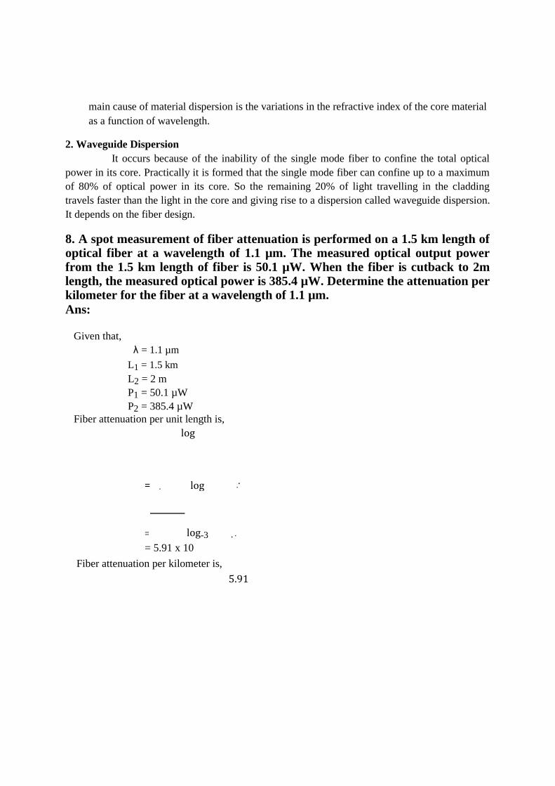
main cause of material dispersion is the variations in the refractive index of the core material
as a function of wavelength. 2. Waveguide Dispersion
It occurs because of the inability of the single mode fiber to confine the total optical
power in its core. Practically it is formed that the single mode fiber can confine up to a maximum
of 80% of optical power in its core. So the remaining 20% of light travelling in the cladding
travels faster than the light in the core and giving rise to a dispersion called waveguide dispersion.
It depends on the fiber design.
8. A spot measurement of fiber attenuation is performed on a 1.5 km length of optical fiber at a wavelength of 1.1 µm. The measured optical output power from the 1.5 km length of fiber is 50.1 µW. When the fiber is cutback to 2m length, the measured optical power is 385.4 µW. Determine the attenuation per kilometer for the fiber at a wavelength of 1.1 µm. Ans:
Given that, λ = 1.1 µm
L1 = 1.5 km
L2 = 2 m
P1 = 50.1 µW
P2 = 385.4 µW Fiber attenuation per unit length is,
log
= . log ..
=
log-3
. .
= 5.91 x 10
Fiber attenuation per kilometer is, 5.91

9. (i) Convert the optical signal power of 5 mW and 20 µW to dBm. (ii) Convert optical signal power of 0.3 mW and 80 nW to dBµ.
Ans: The optical signal power can be expressed in decibels by using,
10 log
Where,
Po = Received optical signal power
Pr = Reference power level
(i) For 1 mW reference power level
10log
Hence the given optical signal power is 5 mW
Optical signal power = 10 log
= 6.98 dBm
= 10 log 5
For 20 µW
10 log
=
Optical signal power =
0.02
10 log
= -16.98 dBm. (ii) For a 1 µW reference power level
10 log
.
For 0.3 mW is equivalent to
Optical signal power =
10 log
=
24.77 dBµ
= 10 log 300
For 800 nW is equivalent is
=
10 log
Optical signal power =
10.97 dBµ
= -10 log 0.08

10. Describe eye pattern analysis for assessing the performance of digital fiber optic link. Is it possible to estimate BER also from eye patterns?
Ans: Eye pattern is a simple and powerful technique in measuring the capacity and
performance of a digital transmission system. The measurements are in time domain and the
waveform distortion can be seen on the CRO immediately. These eye patterns are formed by
superimposing the 2N
possible combinations of N-bit long NRZ patterns.
As said, we need a variety of word patterns to measure the performance of a system using
eye-pattern technique, these word patterns are provided by pseudo random bit generator. This
pseudo random data (bit) pattern generator produces a random data signal that contains 1's and 0's
in a random fashion providing uniform data rate. The random data from pseudo random data
pattern generator is applied to the vertical input of CRO and the data rate triggers the horizontal
sweep. This generates an eye-pattern. For example, consider 8 possible 3-bit NRZ patterns as
shown in following figure 8.10.2.
An eye pattern is obtained by superimposing the above 8 patterns as shown in figure 8.10.3

1. The eye-width opening defines the Inter Symbol Interference (ISI) error free sampling rate
of signal. 2. The best sampling rate is obtained when the height of eye is maximum.
3. One cannot recognize 1's and 0's if height of eye is reduced.
4. The eye height at a particular sampling period gives noise margin. It is given by,
Noise margin = X 100%
5. The system's sensitivity to time is determined by the closing rate of eye for a variation in
sampling period.
6. One can also get rise and fall times of the system from the pattern.
7. Bit Error Rate (BER) is also estimated from the patterns and it can be reduced by inserting
a small amount of redundancy into the transmitted pulse train.