unit 3: transistor at low frequencies - ajay...
TRANSCRIPT

Unit 3: Transistor at Low Frequencies
BJT Transistor Modeling
• A model is an equivalent circuit that represents the AC characteristics of the transistor.
• A model uses circuit elements that approximate the behavior of the transistor.
• There are two models commonly used in small signal AC analysis of a transistor:
– re model
– Hybrid equivalent model
The re Transistor Model
• BJTs are basically current-controlled devices; therefore the re model
uses a diode and a current source to duplicate the behavior of the
transistor.
• One disadvantage to this model is its sensitivity to the DC level. This
model is designed for specific circuit conditions.
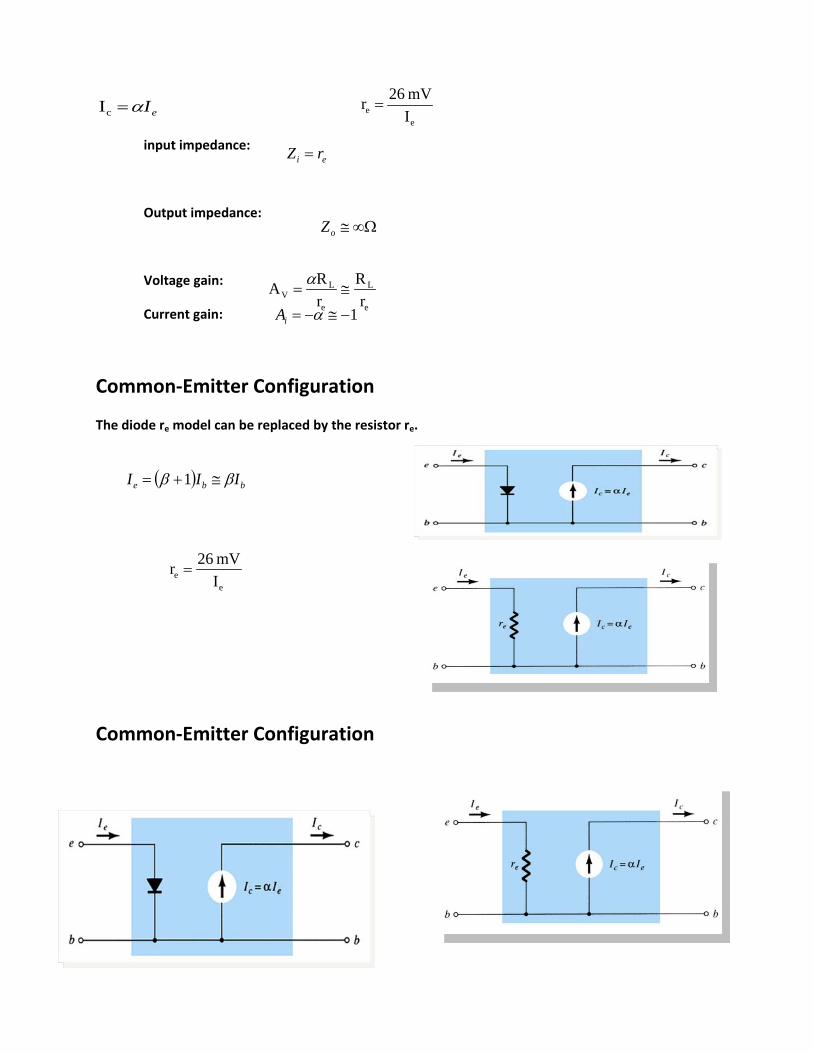
Common-Base Configuration
ee I
mV 26r =
ei rZ =
Ω∞≅oZ
e
L
e
LV r
RrRA ≅=
α
1−≅−= αiA
( ) bbe III ββ ≅+= 1
ee I
mV 26r =
∞==oriA β
eIα Ic =
input impedance:
Output impedance:
Voltage gain:
Current gain:
Common-Emitter Configuration
The diode re model can be replaced by the resistor re.
Common-Emitter Configuration

ei rZ β=
Ω∞≅= oo rZ
e
LV r
RA −=
∞==oriA β
ei rZ )1( += β
Eeo RrZ ||=
eE
EV rR
RA+
=
1Ai += β
Input impedance:
Output impedance:
Voltage gain:
Current gain:
Common-Collector Configuration
Input impedance:
Output impedance:
Voltage gain:
Current gain:

The Hybrid Equivalent Model
The following hybrid parameters are developed and used for modeling the transistor. These parameters can be found on the specification sheet for a transistor.
• hi = input resistance
• hr = reverse transfer voltage ratio (Vi/Vo) ≅ 0
• hf = forward transfer current ratio (Io/Ii)
• ho = output conductance
Simplified General h-Parameter Model
• hi = input resistance
• hf = forward transfer current ratio (Io/Ii)
acfe
eie
hrhββ
==
1−≅−==
αfb
eib
hrh
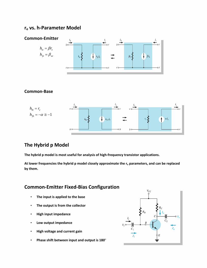
re vs. h-Parameter Model
Common-Emitter
Common-Base
The Hybrid p Model
The hybrid p model is most useful for analysis of high-frequency transistor applications.
At lower frequencies the hybrid p model closely approximate the re parameters, and can be replaced by them.
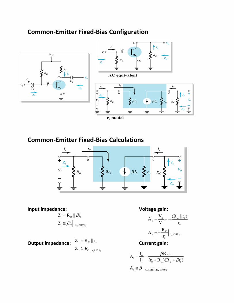
Common-Emitter Fixed-Bias Configuration
• The input is applied to the base
• The output is from the collector
• High input impedance
• Low output impedance
• High voltage and current gain
• Phase shift between input and output is 180°
eE r10Rei
eBi
rZ
r||RZ
ββ
β
≥≅
=
Co
O
10ro
Co
Z
r||RZ
RCR ≥≅
=Co 10Rr
e
Cv
e
oC
i
ov
r
RA
r)r||(R
VVA
≥−=
−==
eBCo r10R ,10Rri
eBCo
oB
i
oi
A
)r)(RR(rrR
IIA
ββ
ββ
≥≥≅
++==
Common-Emitter Fixed-Bias Configuration
Common-Emitter Fixed-Bias Calculations
Input impedance: Voltage gain:
Output impedance: Current gain:

C
ivi R
ZAA −=
ei
21
r||RZR||RRβ′=
=′
Co 10RrCo
oCo
RZ
r||RZ
≥≅
=
Co 10Rre
C
i
ov
e
oC
i
ov
rR
VVA
rr||R
VVA
≥−≅=
−==
Current gain from voltage gain:
Common-Emitter Voltage-Divider Bias
re model requires you to determine β, re, and ro.
Calaculations:
Input impedance:
Output impedance:
Voltage gain:

eCo
Co
r10R ,10Rri
oi
10Rrei
oi
eCo
o
i
oi
IIA
rRR
IIA
)rR)(R(rrR
IIA
ββ
ββ
ββ
≥′≥
≥
≅=
+′′
≅=
+′+′
==
C
ivi R
ZAA −=
Eb
Eeb
Eeb
bBi
RZ)R(rZ1)R(rZ
Z||RZ
ββ
ββ
≅+≅
++==
Co RZ =
Current gain:
Current gain from voltage gain:
Common-Emitter Emitter-Bias Configuration
Impedance Calculations
Input impedance:
Output impedance:

Eb
Eeb
RZE
C
i
ov
)R(rZEe
C
i
ov
b
C
i
ov
RR
VVA
RrR
VVA
ZR
VVA
β
β
β
≅
+=
−≅=
+−==
−==
bB
B
i
oi ZR
RIIA
+==
β
C
ivi R
ZAA −=
Gain Calculations
Voltage gain:
Current gain:
Current gain from voltage gain:
Emitter-Follower Configuration
• This is also known as the common-collector configuration.
• The input is applied to the base and the output is taken from the emitter.
There is no phase shift between input and output.

eE rReo
eEo
rZ
r||RZ
>>≅
=
Eb
Eeb
Eeb
bBi
RZ)R(rZ1)R(rZ
Z||RZ
β≅
+β≅
+β+β=
=
EeEeE RrR ,rRi
ov
eE
E
i
ov
1VVA
rRR
VVA
≅+>>≅=
+==
bB
Bi ZR
RA+
−≅β
Impedance Calculations
Input impedance:
Output impedance:
Gain Calculations
Voltage gain:
Current gain:

E
ivi R
ZAA −=
eEi r||RZ =
Current gain from voltage gain:
Common-Base Configuration
• The input is applied to the emitter.
• The output is taken from the collector.
• Low input impedance.
• High output impedance.
• Current gain less than unity.
• Very high voltage gain.
• No phase shift between input and output.
Calculations
Input impedance:
Co RZ =
e
C
e
C
i
ov r
RrR
VVA ≅==
α
1IIA
i
oi −≅−== α
F
C
ei
RR1
rZ+
=
β
Output impedance:
Voltage gain:
Current gain:
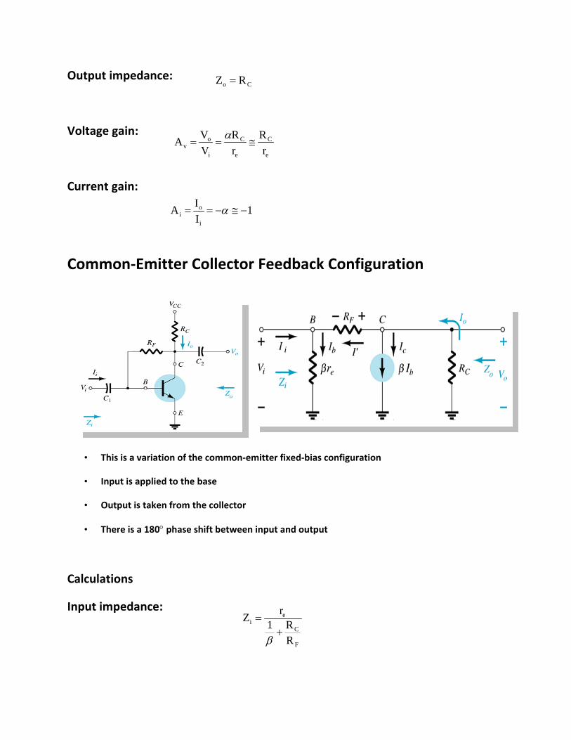
Common-Emitter Collector Feedback Configuration
• This is a variation of the common-emitter fixed-bias configuration
• Input is applied to the base
• Output is taken from the collector
• There is a 180° phase shift between input and output
Calculations
Input impedance:

FCo R||RZ ≅
e
C
i
ov r
RVVA −==
C
F
i
oi
CF
F
i
oi
RR
IIA
RRR
IIA
≅=
+==
ββ
Output impedance:
Voltage gain:
Current gain:
Collector DC Feedback Configuration
• This is a variation of the common-emitter, fixed-bias configuration
• The input is applied to the base
• The output is taken from the collector
• There is a 180° phase shift between input and output
F
C
ei
RR1
rZ+
=
β
FCo R||RZ ≅
e
C
i
ov r
RVVA −==
C
F
i
oi
CF
F
i
oi
RR
IIA
RRR
IIA
≅=
+==
ββ
Calculations
Input impedance:
Output impedance:
Voltage gain:
Current gain:
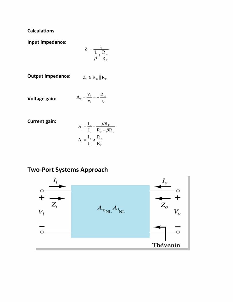
Two-Port Systems Approach
ooTh RZZ ==
ivNLTh VAE =
L
ivi R
ZAA −=
vNLoL
L
i
ov A
RRR
VV
A+
==
This approach:
• Reduces a circuit to a two-port system
• Provides a “Thévenin look” at the output terminals
• Makes it easier to determine the effects of a changing load
With Vi set to 0 V:
The voltage across the open terminals is:
where AvNL is the no-load voltage gain.
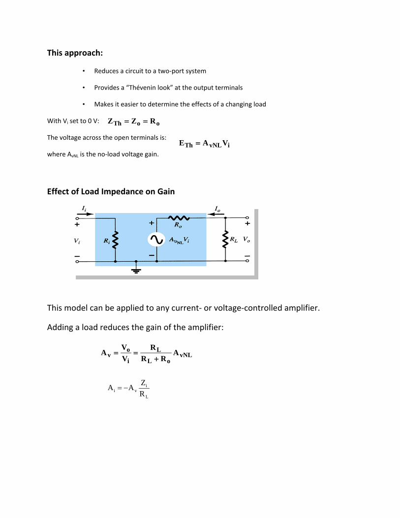
Effect of Load Impedance on Gain
This model can be applied to any current- or voltage-controlled amplifier.
Adding a load reduces the gain of the amplifier:
si
sii RR
VRV+
=
vNLsi
i
s
ovs A
RRR
VVA
+==
L
ivi
oL
vNLL
i
ov
RR
AA
RRAR
VV
A
−=
+==
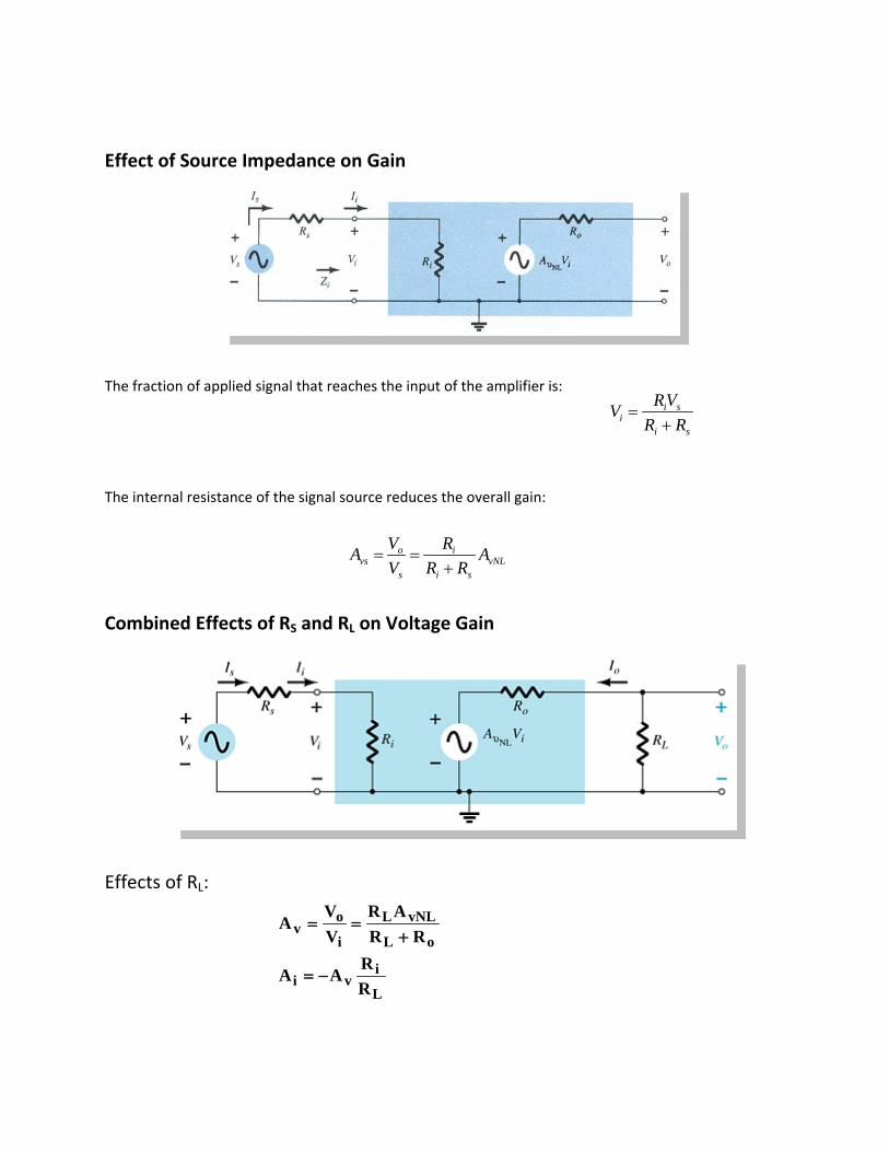
Effect of Source Impedance on Gain
The fraction of applied signal that reaches the input of the amplifier is:
The internal resistance of the signal source reduces the overall gain:
Combined Effects of RS and RL on Voltage Gain
Effects of RL:

L
isvsis
vNLoL
L
si
i
s
ovs
RRR
AA
ARR
RRR
RVV
A
+−=
++==
Co RZ =
ei rRRZ β|||| 21=
Effects of RL and RS:
Cascaded Systems
The output of one amplifier is the input to the next amplifier
The overall voltage gain is determined by the product of gains of the individual stages
The DC bias circuits are isolated from each other by the coupling capacitors
The DC calculations are independent of the cascading
The AC calculations for gain and impedance are interdependent
R-C Coupled BJT Amplifiers
Input impedance, first stage:
Output impedance, second stage:

21
2
211
||||||
vvv
e
CV
e
eCv
AAArRA
rrRRRA
=
=
=β
Voltage gain: