unit e1 (paper version of on-screen assessment) · 2012-07-08 · gcse 4161/01 electronics unit e1...
TRANSCRIPT

GCSE
4161/01
ELECTRONICSUNIT E1(Paper version of on-screen assessment)
A.M. WEDNESDAY, 8 June 2011
1 hour
JD*(S11-4161-01)
Candidate Name
Candidate Number
CentreNumber
0
ADDITIONAL MATERIALS
Information sheet.In addition to this examination paper you may need a calculator.
INSTRUCTIONS TO CANDIDATES
Use black ink or black ball-point pen.Write your name, centre number and candidate number in the spaces at the top of this page.Answer all the questions in the spaces provided in this booklet.
INFORMATION FOR CANDIDATES
The number of marks is given in brackets at the end of each question or part-question.
Total Mark
For Examiner’s use only
4161
0100
01

P = VI = I R = .2 VR
2
VOUT
R
R RV2
1 2S=
+×
INFORMATION SHEET FOR UNIT E1
This information may be of use in answering the questions.
1. Resistor ColourCodes
BLACK 0
BROWN 1
RED 2
ORANGE 3
YELLOW 4
GREEN 5
BLUE 6
VIOLET 7
GREY 8
WHITE 9
The fourth bandcolour gives thetolerance as follows:
GOLD ± 5%
SILVER ± 10%
2. Preferred Values for Resistors – E24 series
10, 11, 12, 13, 15, 16, 18, 20, 22, 24, 27, 30, 33, 36, 39, 43, 47, 51, 56, 62, 68, 75, 82, 91.
7. Power = voltage × current;
8. LED The forward voltage drop across an LED is 2V.
9. NPN Transistors (i) Current gain =
(ii) The forward voltage drop across the base emitter junction is 0·7V.
voltagecurrent
; R = VI
.3. Resistance =
4. Effective resistance, R, of two resistors R1
and R2
in series is given by R = R1
+ R2.
5. Effective resistance, R, of two resistors R1
and R2
in parallel is given by
6. Voltage Divider + VS
0V
R1
R2
Collector currentBase current
h = ; .FEC
B
II
R = R RR R
1 2
1 + 2.
2
(4161-01)

3Examiner
only
(4161-01) Turn over.
Answer all questions.
1. Here is a list of electronic components.
thyristor LED resistor LDR
Give the correct name for each component below.
2. The following electronic sub-systems can be used to build larger systems.
Buzzer Latch unit Delay unit Light sensing unit
Give the names of the sub-systems that answer the questions below.
(a) Which of these sub-systems is an input sub-system?
(b) Which of these sub-systems can keep an output on for a short amount of time and reset automatically?
(c) Which of these sub systems is an output sub-system?
[3]
4161
0100
03
[3]
. . . . . . . . . . . . . . . . . . . . . . . . . . . . . . . . . . . . . . . . . . . . . . . . . . . . . . . . . . . . . . .
. . . . . . . . . . . . . . . . . . . . . . . . . . . . . . . . . . . . . . . . . . . . . . . . . . . . . . . . . . . . . . .
. . . . . . . . . . . . . . . . . . . . . . . . . . . . . . . . . . . . . . . . . . . . . . . . . . . . . . . . . . . . . . .
. . . . . . . . . . . . . . . . . . . . . . . . . . . . . . . . . . . . . . . . . . . . . . . . . . . . . . . . . . . . . . .
. . . . . . . . . . . . . . . . . . . . . . . . . . . . . . . . . . . . . . . . . . . . . . . . . . . . . . . . . . . . . . .
. . . . . . . . . . . . . . . . . . . . . . . . . . . . . . . . . . . . . . . . . . . . . . . . . . . . . . . . . . . . . . .

4Examiner
only
(4161-01)
3. The following are three units of resistance.
kilohm (kΩ) megohm (MΩ) ohm (Ω)
Write the name of each unit in the boxes below so that they are in order of increasing size.
4. Study the following circuit containing three resistors.
Circle the correct answer from the choices given.
(a) What is the value of I2?
0 mA 1 mA 2 mA 3 mA 4 mA 5 mA 6 mA 7 mA 8 mA 9 mA[1]
(b) What is the value of I4?
0 mA 1 mA 2 mA 3 mA 4 mA 5 mA 6 mA 7 mA 8 mA 9 mA[1]
(c) What is the value of V2?
0 V 1 V 2 V 3 V 4 V 5 V 6 V 7 V 8 V 9 V[1]
(d) What is the value of V3?
0 V equal to V1 equal to V2 10V[1]
10 V
0 V
I2
V3V2
I3 = 4mA
I4
I1 = 7mA
V1 = 4V
[1]
Smallest Largest

5Examiner
only
(4161-01) Turn over.
6 V 12 V 6 V12 V
V+
V–
5. Here are 4 lamps.
(a) Which lamp is using the least power? . . . . . . . . . . . . . . . . . . . . . . . . . . . . . . . . . . . . . . . . [1]
(b) Calculate the power in mW for lamp B.
. . . . . . . . . . . . . . . . . . . . . . . . . . . . . . . . . . . . . . . . . . . . . . . . . . . . . . . . . . . . . . . . . . . . . . . . . . . . . . . . . . . . . . . . . . . . . . . . . . . . . . . . . . . . . . . . . . . . . . . . . . . . . . . . . . . . . . . . . . . . . . . . . . . . . . . . . . . . . . . . . . . . . . . . . . . . . . . . . . . . . . . . . . . . . . . . . . . . . . . . . . . . . . . . . . . . . . .
. . . . . . . . . . . . . . . . . . . . . . . . . . . . . . . . . . . . . . . . . . . . . . . . . . . . . . . . . . . . . . . . . . . . . . . . . . . . . . . . . . . . . . . . . . . . . . . . . . . . . . . . . . . . . . . . . . . . . . . . . . . . . . . . . . . . . . . . . . . . . . . . . . . . . . . . . . . . . . . . . . . . . . . . . . . . . . . . . . . . . . . . . . . . . . . . . . . . . . . . . . . . . . . . . . . . . . .
[1]
6. The following diagram shows the pinout of a comparator IC.
Write the following labels next to the correct pins on the comparator IC.
Negative Supply Pin Non-inverting Input Pin Output Pin[3]
_
+
0.5mA 0.5mA 0.3mA0.3mA
4161
0100
05
. . . . . . . . . . . . . . . . . . . . . . . . . . . . . . . . . . . . . . . . . . . . . . . . . . . . . . . . . . . . . . . . . . . . . . . . . . . . . . . . . . . . . . . . . . . . . . . . . . . . . . . . . . . . . . . . . . . . . . . . . . . . . .
. . . . . . . . . . . . . . . . . . . . . . . . . . . . . . . . . . . . . . . . . . . . . . . . . . . . . . . . . . . . . . . . . . . . . . . . . . . . . . . . . . . . . . . . . . . . . . . . . . . . . . . . . . . . . . . . . . . . . . . . . . . . . .
. . . . . . . . . . . . . . . . . . . . . . . . . . . . . . . . . . . . . . . . . . . . . . . . . . . . . . . . . . . . . . . . . . . . . . . . . . . . . . . . . . . . . . . . . . . . . . . . . . . . . . . . . . . . . . . . . . . . . . . . . . . . . .
. . . . . . . . . . . . . . . . . . . . . . . . . . . . . . . . . . . . . . . . . . . . . . . . . . . . . . . . . . . . . . . . . . . . . . . . . . . . . . . . . . . . . . . . . . . . . . . . . . . . . . . . . . . . . . . . . . . . . . . . . . . . . .

6Examiner
only
(4161-01)
7. A hazard beacon warns drivers about a skip at the side of the road. It flashes on and off continuously when it gets dark, and switches off in daylight. The following sub-systems are available.
Thyristor OR gate Pulse Generator Temperature Sensing Unit Buzzer unit
Time Delay Lamp Unit Light Sensing Unit AND gate Transistor Switch
Select the correct sub-systems to complete the block diagram.
(a) Write down the value of this resistor in ohms. . . . . . . . . . . . . . . . . . . . . . . . . . . . . . . . . . . . . . . . . . . . . . . . . . . . . . . . . [3]
(b) What is the tolerance of this resistor? Circle the correct answer.
±1% ±2% ±5% ±10% ±20% [1]
8. The diagram shows a resistor.
Band 1 - Orange Band 3 - Red
Band 2 - White Band 4 - Silver
[5]

7Examiner
only
(4161-01) Turn over.
9. The circuit shows some diodes and lamps connected to a battery.
L1
L4
S
L2
L3
The Switch S is now closed. Which lamp, L1, L2, L3 or L4, will NOT light up?
. . . . . . . . . . . . . . . . . . . . . . . . . . . . . . . . . . . . . . . . . . . . . . . . . . . . . . [1]
4161
0100
07

8Examiner
only
(4161-01)
14 13 12 11 10 9 8
1 2 3 4 5 6 7
X
11. Here is the pinout for a logic gate IC.
(a) How many logic gates are there on the IC? . . . . . . . . . . . . . . . . . . . . . . . . . . . . . . . . . . . . . . . . [1]
(b) What is the pin number of the output of logic gate X? . . . . . . . . . . . . . . . . . . . . . . . . . . . . . . . . . . . . . . . . [1]
(a) Circle the name of the component labelled X.
Resistor Variable Resistor LED Thermistor[1]
(b) VOUT = 2 V. Circle the correct voltage across the component X.
0 V 1 V 2 V 3 V 4 V 5 V 6 V 7 V 8 V 9 V[1]
(c) What happens to the resistance of the LDR when the light level increases? Tick (√) the correct answer.
It increases
It stays the same
It decreases
It depends on how good the battery is [1]
10. Here is the circuit diagram for a light sensing unit containing an LDR.
9 V
X VX
VOUT
0 V

9Examiner
only
(4161-01) Turn over.
13. (a) Circle the name of the logic gate that has the following truth table. [1]
AND gate NAND gate NOR gate NOT gate OR gate
(b) Circle the name of the logic gate that outputs a logic 0 signal only when both inputs are at logic 1. [1]
AND gate NAND gate NOR gate NOT gate OR gate
Inputs Output
0 0
0 1
0
1
A B Q
0
1
1
1
1 1
12. The following list gives the names of some logic gates.
AND gate NAND gate NOR gate NOT gate OR gate
Use the correct logic gate name for the symbols below.
(a) (b) (c)
. . . . . . . . . . . . . . . . . . . . . . . . . . . . . . . . . . . . . . . . . . . . . . . . . . . . . . . . . . . . . . . . . . . . . . . . . . . . . . . . . . . . . . . . . .. . . . . . . . . . . . . . . . . . . . . . . . . . . . . . . . . . . . . . . . . . . . . [3]
4161
0100
09
10Examiner
only
(4161-01)
15. (a) Here is a diagram for a MOSFET.
Select from the list of terminal names below, to label the diagram.
Base Collector Drain Source Emitter Gate [3]
(b) Why is a MOSFET often used instead of a transistor to interface a logic system to a motor?
. . . . . . . . . . . . . . . . . . . . . . . . . . . . . . . . . . . . . . . . . . . . . . . . . . . . . . . . . . . . . . . . . . . . . . . . . . . . . . . . . . . . . . . . . . . . . . . . . . . . . . . . . . . . . . . . . . . . . . . . . . . . . . . . . . . . . . . . . . . . . . . . . . . . . . . . . . . . . . . . . . . . . . . . . . . . . . . . . . . . . . . . . . . . . . . . . . . . . . . . . . . . . . . . . . . . . . .
. . . . . . . . . . . . . . . . . . . . . . . . . . . . . . . . . . . . . . . . . . . . . . . . . . . . . . . . . . . . . . . . . . . . . . . . . . . . . . . . . . . . . . . . . . . . . . . . . . . . . . . . . . . . . . . . . . . . . . . . . . . . . . . . . . . . . . . . . . . . . . . . . . . . . . . . . . . . . . . . . . . . . . . . . . . . . . . . . . . . . . . . . . . . . . . . . . . . . . . . . . . . . . . . . . . . . . .
. . . . . . . . . . . . . . . . . . . . . . . . . . . . . . . . . . . . . . . . . . . . . . . . . . . . . . . . . . . . . . . . . . . . . . . . . . . . . . . . . . . . . . . . . . . . . . . . . . . . . . . . . . . . . . . . . . . . . . . . . . . . . . . . . . . . . . . . . . . . . . . . . . . . . . . . . . . . . . . . . . . . . . . . . . . . . . . . . . . . . . . . . . . . . . . . . . . . . . . . . . . . . . . . . . . . . . .
[1]
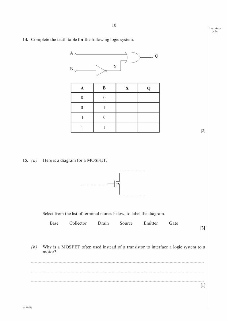
A
B X
Q
0 0
0
A B X Q
0
1
1
1
1[2]
14. Complete the truth table for the following logic system.
. . . . . . . . . . . . . . . . . . . . . . . . . . . . . . . . . . .
. . . . . . . . . . . . . . . . . . . . . . . . . . . . . . . . . . .
. . . . . . . . . . . . . . . . . . . . . . . . . . . . . . . . . . .

11Examiner
only
(4161-01) Turn over.
16. The circuit diagram shows part of a system used to switch on an alarm.
VIN
0.4 V
2.2 V
Buzzer On / Off?
Write either the word ‘ON’ or ‘OFF’ to show what happens to the buzzer for each value of VIN.
17. The diagram below shows two resistors connected in parallel.
What is the resistance between A and B? Circle the correct answer.
1 kΩ 1.5 kΩ 2 kΩ 2.5 kΩ 3 kΩ 3.5 kΩ 4 kΩ 4.5 kΩ 5 kΩ 5.5 kΩ 6 kΩ[1]
A B
3kΩ
3kΩ
12 V
0 V
RInput
Buzzer
VIN
4161
0100
11
[1]

12Examiner
only
(4161-01)
18. Here are two truth tables. For each of the following, tick (√) the correct Boolean equation that represents the function
described by the truth table.
(a)
0 0
0 1
0
1
Input A Input B Output Q
0
1
1
1
1 1
Answer:
Q = A.B
Q = A + B
Q = A.B
Q = A + B
0 0
0 0
0
1
Input A Input B Output Q
0
1
1
1
1 0
Answer:
Q = A.B
Q = A + B
Q = A.B
Q = A + B
(b)
[1]
[1]

13Examiner
only
(4161-01) Turn over.
19. The following diagrams show some arrangements of NAND gates. For each arrangement tick (√) the equivalent ‘standard’ gate.
(a) Answer:
NOT Gate
AND Gate
OR Gate
NOR Gate[1]
Answer:
NOT Gate
AND Gate
OR Gate
NOR Gate[1]
(b)
Answer:
NOT Gate
AND Gate
OR Gate
NOR Gate[1]
(c)
A Q
A
B
Q
A
B
Q

14Examiner
only
(4161-01)
20. Some of the NAND gates in the logic circuit below are redundant.
Cross out all of the redundant NAND gates.
[2]
A
B
C
Q

15Examiner
only
(4161-01) Turn over.
21. Here is part of an alarm circuit.
(a) Draw the two components required in boxes P and Q so that Input A receives a logic 0 input to the logic system when a switch S1 is pressed.
(b) What combination of switch settings will cause the output of the AND gate to be high?
S1 Off & S2 Off, S1 On & S2 Off, S1 Off & S2 On, S1 On & S2 On
Circle the correct answer.[1]
S1
S2
QA
B
0V
9V
P
Q
[1]

16Examiner
only
(4161-01)
22. The following diagram shows a comparator. The comparator saturates at +1.5V and +8.5V.
_
+
The output of the comparator is:
0.3V
1.5V
5.9V
6.2V
8.5V
12.1V Tick (√) the correct answer.[1]
6.2 V
5.9 V
Vout

17Examiner
only
(4161-01)
9 V
0 V
5kΩ
X
Y R
20kΩ
10kΩ
(a) When the temperature rises, the resistance of the thermistor:
increases
stays the same
decreases
doubles Tick (√) the correct answer.[1]
(b) Calculate the voltage at the inverting input ‘Y’.
. . . . . . . . . . . . . . . . . . . . . . . . . . . . . . . . . . . . . . . . . . . . . . . . . . . . . . . . . . . . . . . . . . . . . . . . . . . . . . . . . . . . . . . . . . . . . . . . . . . . . . . . . . . . . . . . . . . . . . . . . . . . . . . . . . . . . . . . . . . . . . . . . . . . . . . . . . . . . . . . . . . . . . . . . . . . . . . . . . . . . . . . . . . . . . . . . . . . . . . . . . . . . . . . . . . . . . .
. . . . . . . . . . . . . . . . . . . . . . . . . . . . . . . . . . . . . . . . . . . . . . . . . . . . . . . . . . . . . . . . . . . . . . . . . . . . . . . . . . . . . . . . . . . . . . . . . . . . . . . . . . . . . . . . . . . . . . . . . . . . . . . . . . . . . . . . . . . . . . . . . . . . . . . . . . . . . . . . . . . . . . . . . . . . . . . . . . . . . . . . . . . . . . . . . . . . . . . . . . . . . . . . . . . . . . .
[1]
_
+
23. The following circuit shows a comparator which is configured as a fire alarm.
D1
–t
VT
Turn over.

18Examiner
only
(4161-01)
24. An LED is to be used as a power-on indicator as shown below. The LED passes a current of 10mA .
(a) What is the current through resistor R? . . . . . . . . . . . . . . . . . . . . . . . . . . . . . . . . . . . . . . . . . . . . . . . . . . . . . . . . . . . . . mA[1]
(b) What is the voltage drop across the resistor R? . . . . . . . . . . . . . . . . . . . . . . . . . . . . . . . . . . . . . . . . . . . . . . . . . . . . . . . . . . . . . V[1]
(c) What is the ideal resistance of resistor R? . . . . . . . . . . . . . . . . . . . . . . . . . . . . . . . . . . . . . . . . . . . . . . . . . . . . . . . . . . . . . Ω[1]
(d) Select the preferred value resistor that would ensure that the current through the LED is no more than 10mA. (Circle the correct answer)
100 Ω 220 Ω 270 Ω 330 Ω 390 Ω 470 Ω 560 Ω 820 Ω 1000 Ω[1]
R
2 V
9 V
0 V

GCSE
4161/01-A
ELECTRONICSCANDIDATE INFORMATION SHEET FOR UNIT E1
A.M. WEDNESDAY, 8 June 2011
CJ*(S11-4161-01A)

P = VI = I R = .2 VR
2
VOUT
R
R RV2
1 2S=
+×
INFORMATION SHEET FOR UNIT E1
This information may be of use in answering the questions.
1. Resistor ColourCodes
BLACK 0
BROWN 1
RED 2
ORANGE 3
YELLOW 4
GREEN 5
BLUE 6
VIOLET 7
GREY 8
WHITE 9
The fourth bandcolour gives thetolerance as follows:
GOLD ± 5%
SILVER ± 10%
2. Preferred Values for Resistors – E24 series
10, 11, 12, 13, 15, 16, 18, 20, 22, 24, 27, 30, 33, 36, 39, 43, 47, 51, 56, 62, 68, 75, 82, 91.
7. Power = voltage × current;
8. LED The forward voltage drop across an LED is 2V.
9. NPN Transistors (i) Current gain =
(ii) The forward voltage drop across the base emitter junction is 0·7V.
voltagecurrent
; R = VI
.3. Resistance =
4. Effective resistance, R, of two resistors R1
and R2
in series is given by R = R1
+ R2.
5. Effective resistance, R, of two resistors R1
and R2
in parallel is given by
6. Voltage Divider + VS
0V
R1
R2
Collector currentBase current
h = ; .FEC
B
II
R = R RR R
1 2
1 + 2.
2
(4161-01A)