unit - i light emitting diodes - ernasugesti's blog · many small particles called photons....
TRANSCRIPT

UNIT - I
Light Emitting Diodes
Periyanayaga Kristy.A,
Ph.D. Research Scholar
SRM University
Chennai

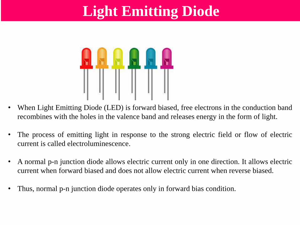
Light Emitting Diode
In 1879, Edison invented the incandescent light bulb.
In the light bulb, an electric current is passed through a filament
inside the bulb. When sufficient current is passed through the
filament, it gets heated up and emits light.
The light emitted by the filament is the result of electrical energy
converted into heat energy which in turn changes into light energy.
In Light Emitting Diodes (LEDs), electrical energy flowing through
it is directly converted into light energy.
Light is a type of energy that can be released by an atom. Light is made up of
many small particles called photons.
Atoms are the basic building blocks of matter.
Atoms are made up of small particles such as electrons, protons and neutrons.

Light Emitting Diode
• The attractive force between the protons and neutrons makes them stick
together to form nucleus. Neutrons have no charge. Hence, the overall charge of
the nucleus is positive.
• The negatively charged electrons always revolve around the positively charged
nucleus because of the electrostatic force of attraction between them. Electrons
revolve around the nucleus in different orbits or shells. Each orbit has different
energy level.

Light Emitting Diode
• The electrons in the higher energy level will not stay for long period. After a
short period, the electrons fall back to lower energy level.
• The electrons which jump from higher energy level to lower energy level will
releases energy in the form of a photon or light.
• In some materials, this energy lose is released mostly in the form of heat. The
electron which loses greater energy will releases a greater energy photon.
• The Light emitting diode is a two-lead semiconductor light source. In 1962, Nick
Holonyak has come up with an idea of light emitting diode, and he was working
for the general electric company.
• The LED is a special type of diode and they have similar electrical characteristics
of a PN junction diode. Hence the LED allows the flow of current in the forward
direction and blocks the current in the reverse direction.

Light Emitting Diode
• Light Emitting Diodes (LEDs) are the most widely used semiconductor diodes among all
the different types of semiconductor diodes available today.
• It emit either visible light (or) invisible infrared light when forward biased. The LEDs
which emit invisible infrared light are used for remote controls.
• The LED occupies the small area which is less than the 1 mm2. The applications of LEDs
used to make various electrical and electronic projects.
Light Emitting Diode
• When Light Emitting Diode (LED) is forward biased, free electrons in the conduction band
recombines with the holes in the valence band and releases energy in the form of light.
• The process of emitting light in response to the strong electric field or flow of electric
current is called electroluminescence.
• A normal p-n junction diode allows electric current only in one direction. It allows electric
current when forward biased and does not allow electric current when reverse biased.
• Thus, normal p-n junction diode operates only in forward bias condition.

Light Emitting Diode
• To create an LED, the n-type material should be connected to the negative terminal of the
battery and p-type material should be connected to the positive terminal of the battery.
• In other words, the n-type material should be negatively charged and the p-type material
should be positively charged.
• The construction of LED is similar to the normal p-n junction diode except that gallium,
phosphorus and arsenic materials are used for construction instead of silicon or germanium
materials.
• In normal p-n junction diodes, silicon is most widely used because it is less sensitive to the
temperature. Also, it allows electric current efficiently without any damage. In some cases,
germanium is used for constructing diodes.
• However, silicon or germanium diodes do not emit energy in the form of light. Instead,
they emit energy in the form of heat.
• Thus, silicon or germanium is not used for constructing LEDs.

Light Emitting Diode
Layers of LED
A Light Emitting Diode (LED) consists of three layers:p-type semiconductor , n-type semiconductor and depletion layer. The p-type
semiconductor and the n-type semiconductor are separated by a depletion region or depletion layer.
P-type semiconductor• When trivalent impurities are added to the intrinsic or pure semiconductor, a p-type
semiconductor is formed.
• In p-type semiconductor, holes are the majority charge carriers and free electrons are the minority charge carriers. Thus, holes carry most of the electric current in p-type semiconductor.
N-type semiconductor• When pentavalent impurities are added to the intrinsic semiconductor, an n-type
semiconductor is formed.
• In n-type semiconductor, free electrons are the majority charge carriers and holes are the minority charge carriers. Thus, free electrons carry most of the electric current in n-type semiconductor.

Light Emitting Diode
Depletion layer or region
Depletion region is a region present between the p-type and n-type semiconductor
where no mobile charge carriers (free electrons and holes) are present.
• This region acts as barrier to the electric current. It opposes flow of electrons from n-type
semiconductor and flow of holes from p-type semiconductor.
• To overcome the barrier of depletion layer, we need to apply voltage which is greater than
the barrier potential of depletion layer.
How Light Emitting Diode (LED) works?
• Light Emitting Diode (LED) works only in forward bias condition. When Light Emitting Diode (LED) is forward biased, the free electrons from n-side and the holes from p-side are pushed towards the junction.
• When free electrons reach the junction or depletion region, some of the free electrons recombine with the holes in the positive ions.
• We know ,that positive ions have less number of electrons than protons.
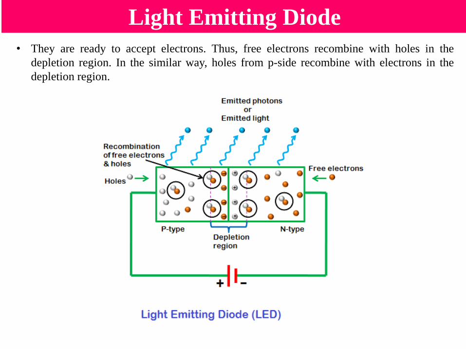
Light Emitting Diode
• They are ready to accept electrons. Thus, free electrons recombine with holes in the
depletion region. In the similar way, holes from p-side recombine with electrons in the
depletion region.

Light Emitting Diode
• Because of the recombination of free electrons and holes in the depletion region, the width
of depletion region decreases.
• As a result, more charge carriers will cross the p-n junction. Some of the charge carriers
from p-side and n-side will cross the p-n junction before they recombine in the depletion
region.
• For example, some free electrons from n-type semiconductor cross the p-n junction and
recombines with holes in p-type semiconductor.
• In the similar way, holes from p-type semiconductor cross the p-n junction and
recombines with free electrons in the n-type semiconductor. Thus, recombination takes
place in depletion region as well as in p-type and n-type semiconductor.
• The free electrons in the conduction band releases energy in the form of light beforethey recombine with holes in the valence band.

Light Emitting Diode
• In silicon and germanium diodes, most of the energy is released in the form of heat and emitted light is too small.
• However, in materials like gallium arsenide and gallium phosphide the emitted photons have sufficient energy to produce intense visible light.
How LED emits light?• When external voltage is applied to the valence electrons , they gain sufficient energy
and breaks the bonding with the parent atom.
• The valence electrons which breaks bonding with the parent atom are called free
electrons.
• When the valence electron left the parent atom, they leave an empty space in the valence
shell at which valence electron left. This empty space in the valence shell is called a
hole.

Light Emitting Diode
• The energy level of free electrons in the conduction band is high compared to the energy
level of valence electrons or holes in the valence band.
• Therefore, free electrons in the conduction band need to
lose energy in order to recombine with the holes in the
valence band.
• The free electrons in the conduction band do not stay
for long period. After a short period, the free electrons
lose energy in the form of light and recombine with
the holes in the valence band. Each recombination of
charge carrier will emit some light energy.
• The energy lose of free electrons or the intensity of emitted light is depends on the forbidden gap or energy gap between conduction band and valence band.

Light Emitting Diode
• In normal silicon diodes, the energy gap between conduction band and valence band is
less. Hence, the electrons fall only a short distance.
• As a result, low energy photons are released. These low energy photons have low
frequency which is invisible to human eye.
• In LEDs, the energy gap between conduction band and valence band is very large so the
free electrons in LEDs have greater energy than the free electrons in silicon diodes.
• Hence, the free electrons fall to a large distance. As a result, high energy photons are
released. These high energy photons have high frequency which is visible to human eye.
• The efficiency of generation of light in LED increases with increase in injected currentand with a decrease in temperature.
• In light emitting diodes, light is produced due to recombination process. Recombinationof charge carriers takes place only under forward bias condition. Hence, LEDs operateonly in forward bias condition.

Light Emitting Diode
• When light emitting diode is reverse biased, the free electrons (majority carriers) from n-side and holes (majority carriers) from p-side moves away from the junction.
• As a result, the width of depletion region increases and no recombination of charge carriers occur. Thus, no light is produced.
• If the reverse bias voltage applied to the LED is highly increased, the device may also be damaged.
• All diodes emit photons or light but not all diodes emit visible light. The material in an LED is selected in such a way that the wavelength of the released photons falls within the visible portion of the light spectrum.
• Light emitting diodes can be switched ON and OFF at a very fast speed of 1 ns.

Light Emitting Diode
• One of the methods used to construct LED is to deposit three semiconductor layers on the substrate. The three semiconductor layers deposited on the substrate are n-type semiconductor, p-type semiconductor and active region.
• Active region is present in between the n-type and p-type semiconductor layers.

Light Emitting Diode
• When LED is forward biased, free electrons from n-type semiconductor and holes from
p-type semiconductor are pushed towards the active region.
• In LED, most of the charge carriers recombine at active region. Therefore, most of thelight is emitted by the active region. The active region is also called as depletion region.
• The safe forward voltage ratings of most LEDs is from 1V to 3 V and forward currentratings is from 200 mA to 100 mA.
• If the voltage applied to LED is in between 1V to 3V, LED works perfectly because thecurrent flow for the applied voltage is in the operating range.
• However, if the voltage applied to LED is increased to a value greater than 3 volts.
• The depletion region in the LED breaks down and the electric current suddenly rises.This sudden rise in current may destroy the device.

Light Emitting Diode
I-V Characteristics of LED
• There are different types of light emitting diodes are available in the market and there are
different LED characteristics which include the color light, or wavelength radiation, light
intensity.
• The important characteristic of the LED is color. In the starting use of LED, there is the
only red color. As the use of LED is increased with the help of the semiconductor process
and doing the research on the new metals for LED, the different colors were formed.
• The amount of output light emitted by the LED is directly proportional to the amount offorward current flowing through the LED.
Visible LEDs and invisible LEDsLEDs are mainly classified into two types: visible LEDs and invisible LEDs.
• Visible LED is a type of LED that emits visible light.
• These LEDs are mainly used for display or illumination where LEDs are used individually without photosensors.
• Invisible LED is a type of LED that emits invisible light (infrared light). These LEDs are mainly used with photosensors such as photodiodes.
Light Emitting Diode
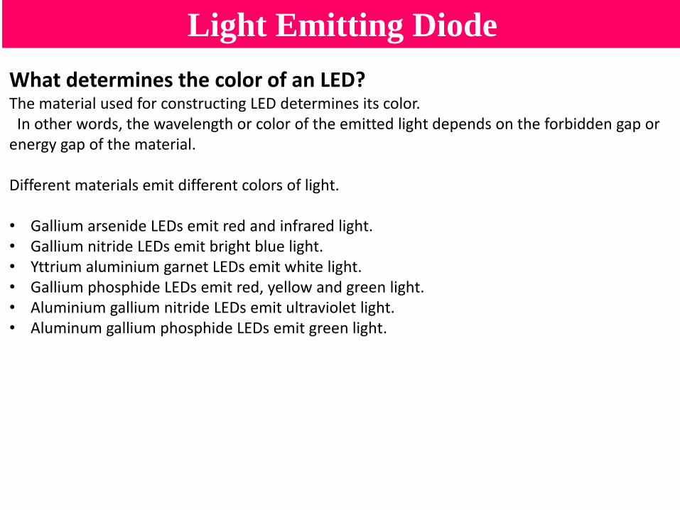
What determines the color of an LED?The material used for constructing LED determines its color.
In other words, the wavelength or color of the emitted light depends on the forbidden gap or energy gap of the material.
Different materials emit different colors of light.
• Gallium arsenide LEDs emit red and infrared light.• Gallium nitride LEDs emit bright blue light.• Yttrium aluminium garnet LEDs emit white light.• Gallium phosphide LEDs emit red, yellow and green light.• Aluminium gallium nitride LEDs emit ultraviolet light.• Aluminum gallium phosphide LEDs emit green light.

Light Emitting Diode

Light Emitting Diode
Applications of Light Emitting Diodes
• There are many applications of the LED and some of them are explained below.
• LED is used as a bulb in the homes and industries
• The light emitting diodes are used in the motorcycles and cars.
• These are used in the mobile phones to display the message.
• At the traffic light signals led’s are used
Advantages of LED’s
• The cost of LED’s is less and they are tiny.
• By using the LED’s the electricity is controlled.
• The intensity of the LED differs with the help of the microcontroller.
Organic - Light Emitting Diode
• What is an OLED?
• An OLED is an electronic device made by placing
a series of organic thin films between two
conductors.
• When electrical current is applied, a bright light is
emitted.
• A device that is 100 to 500 nanometers thick or
about 200 times smaller than a human hair.

Organic - Light Emitting Diode
• The OLED Structure
Organic - Light Emitting Diode
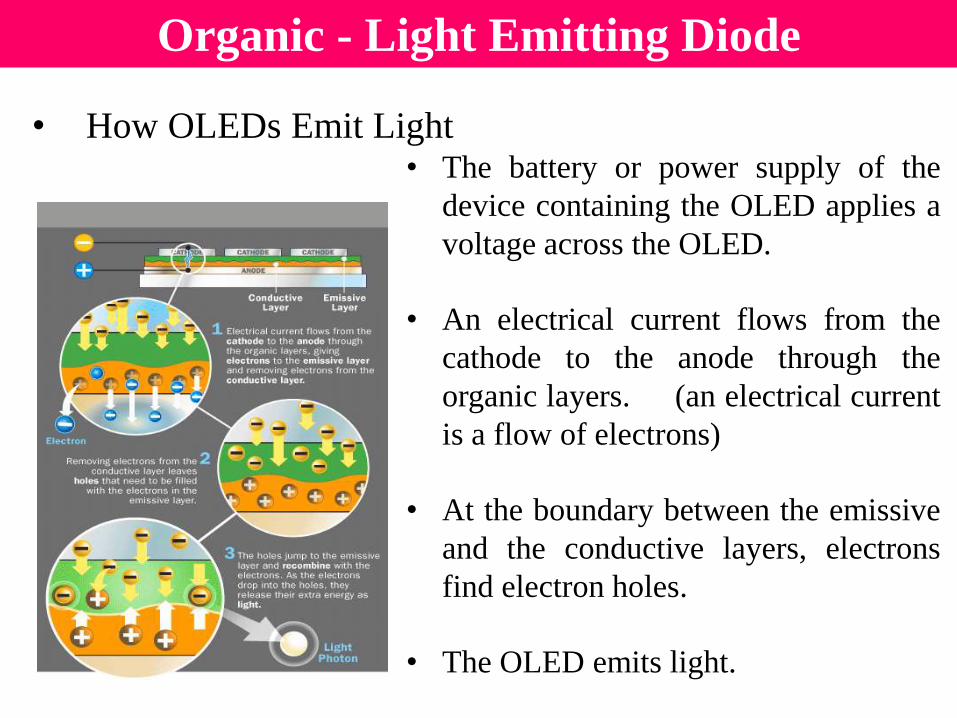
• How OLEDs Emit Light• The battery or power supply of the
device containing the OLED applies a
voltage across the OLED.
• An electrical current flows from the
cathode to the anode through the
organic layers. (an electrical current
is a flow of electrons)
• At the boundary between the emissive
and the conductive layers, electrons
find electron holes.
• The OLED emits light.

Function and structure of an OLED and
nanomaterials it contains
• An OLED is a thin, flat luminous component with a thickness of
usually less than 1 micrometre (μm4).
• It consists of at least one light-emitting layer (emitter layer) made of
organic semiconductor material, is generally built with several layers,
each with a thickness of up to 100 nanometres (nm 5), which are
positioned between two electrodes.
• One or both electrodes of the OLED are transparent such that light can
radiate toward one or both directions and gives it a translucent
appearance when switched of.
• Compared to ILEDs, OLEDs have the advantage that the colour of the
light can be customised to reflect the entire visible spectrum.

Schematic representation of the structure of an OLED
• When switched on, voltage builds up between the electrodes which leads to a drift of the
positive charge (p-holes) and the negative charge (electrons) in the semi-conductor layers
toward each other.
• The charges accumulate in the emitter layer, creating an excited state when hitting each
other: the exciton.
• Depending on the mechanism, this may be the direct excitation of a dyestuff molecule; or
the dyestuff is excited by the energy released when the exciton decays.
• When the excited state of the dyestuff changes back to the basic state, a light particle
(photon) with a defined wavelength is emitted.
• Two types of OLEDs are distinguished: the emitter layer consists of polymers (PLED) or
of small organic molecules (small molecular organic LED = SMOLED).

Physicochemical properties of OLEDsPhotometric capacities
• Luminous flux (lumen, lm): light sources emit radiation within a defined
spectrum.
• The radiant power described with the unit watt captures this emitted
radiation indiscriminately across the entire light spectrum.
• However, the sensitivity of the eye varies for the different wavelengths.
• Taking into account this effect results in the luminous flux, also known as
luminous power, described with the unit lumen (lm).
• Luminous intensity (candela, cd): luminous flux within a defined solid
angle. The luminous intensity rates the light emitted by a light source in a
defined direction.
• Illuminance E (lux, lx or lm/m²): luminous flux cast onto a defined surface.

Physicochemical properties of OLEDsPhotometric capacities
• Luminance (candela per m², cd/m²): luminous flux emitted by a surface in a
defined direction.
• Luminance is the measure that describes what the human eye perceives as
brightness of a surface.
• Luminous efficacy (lamp efficacy, lumen per watt): efficiency of a light
source, that is, the ratio between the benefit (emitted luminous flux) and
expenditures (consumed electric power).
•
• The luminous efficacy describes how much light can be generated with the
used electricity (principle of maximisation).
• However, the goal is generally to keep the required electricity as low as
possible with a given luminous flux (principle of minimisation).
• Consequently, other parameters, such as e.g. the PLI number are preferable.

Organic - Light Emitting Diode

Organic - Light Emitting Diode
Types of OLEDs
• Passive-matrix
• Active-matrix
• Transparent
• Top-emitting
• Flexible
• White

Organic - Light Emitting Diode
Passive-Matrix

Organic - Light Emitting Diode
Passive-Matrix (PMOLED)
• PMOLEDs have strips of cathode, organic layers and strips of anode. The anode strips arearranged perpendicular to the cathode strips.
• The intersections of the cathode and anode make up the pixels where light is emitted.
• External circuitry applies current to selected strips of anode and cathode, determining whichpixels get turned on and which pixels remain off.
• Again, the brightness of each pixel is proportional to the amount of applied current.
• PMOLEDs are easy to make, but they consume more power than other types of OLED,mainly due to the power needed for the external circuitry.
• PMOLEDs are most efficient for text and icons and are best suited for small screens (2- to 3-inch diagonal) such as those you find in cell phones, PDAs and MP3 players.
• Even with the external circuitry, passive-matrix OLEDs consume less battery power than theLCDs that currently power these devices.

Organic - Light Emitting Diode
Active-Matrix

Organic - Light Emitting Diode
Active-Matrix (AMOLED)
• AMOLEDs have full layers of cathode, organic molecules and anode, but the anodelayer overlays a thin film transistor (TFT) array that forms a matrix.
• The TFT array itself is the circuitry that determines which pixels get turned on toform an image.
• AMOLEDs consume less power than PMOLEDs because the TFT array requires lesspower than external circuitry, so they are efficient for large displays.
• AMOLEDs also have faster refresh rates suitable for video.
• The best uses for AMOLEDs are computer monitors, large-screen TVs and electronicsigns or billboards.

Organic - Light Emitting Diode
Transparent OLED

Organic - Light Emitting Diode
Transparent OLED
• Transparent OLEDs have only transparent components(substrate, cathode and anode) and, when turned off, areup to 85 percent as transparent as their substrate.
• When a transparent OLED display is turned on, it allowslight to pass in both directions.
• A transparent OLED display can be either active- or passive-matrix.
• This technology can be used for heads-up displays

Organic - Light Emitting Diode
Top-Emitting OLED

Organic - Light Emitting Diode
Top-Emitting OLED
• Top-emitting OLEDs have a substrate that iseither opaque or reflective.
• They are best suited to active-matrix design.
• Manufacturers may use top-emitting OLEDdisplays in smart cards.

Organic - Light Emitting Diode
Flexible OLED

Organic - Light Emitting Diode
Flexible OLED
• Foldable OLEDs have substrates made of very flexible metallic foilsor plastics. Foldable OLEDs are very lightweight and durable.
• Their use in devices such as cell phones and PDAs can reducebreakage, a major cause for return or repair.
• Potentially, foldable OLED displays can be attached to fabrics tocreate "smart" clothing, such as outdoor survival clothing with anintegrated computer chip, cell phone, GPS receiver and OLED displaysewn into it.

Organic - Light Emitting Diode
White OLED
Organic - Light Emitting Diode
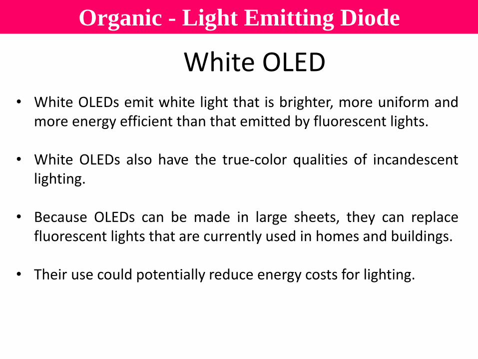
White OLED• White OLEDs emit white light that is brighter, more uniform and
more energy efficient than that emitted by fluorescent lights.
• White OLEDs also have the true-color qualities of incandescentlighting.
• Because OLEDs can be made in large sheets, they can replacefluorescent lights that are currently used in homes and buildings.
• Their use could potentially reduce energy costs for lighting.

Organic - Light Emitting Diode
Advantages
• Thinner, lighter and more flexible
• Brighter
• Consume much less power
• Easier to produce and make into larger sizes
• Large field of view

Organic - Light Emitting Diode
Disadvantages
• Lifetime
• Manufacturing
• Water
Organic - Light Emitting Diode
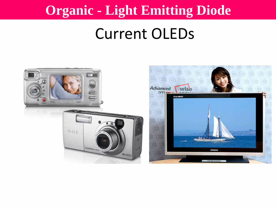
Current OLEDs

Organic - Light Emitting Diode
Future of OLEDs?

OLEDs - Conclusion• The Federal Environment Agency considers OLEDs to be an interesting factor
in the future development of the lighting sector. Compared to conventional
incandescent lamps, the energy requirement to generate a specific luminous
efficiency is lower, while the operating life is at the same time considerably
longer than the one of an incandescent lamp.
• Compared to the widely used energy-saving lamps, OLEDs do not contain
mercury, which might be released in case of breakage. The quantity of included
hazardous substances is extraordinarily small due to the nano-coating and no
health risk is therefore expected even in case of breakage. No release of
nanoparticles in connection with the technology (coating) is expected.
• Only relatively few lighting products containing OLEDs are currently on the
market. Furthermore, they all have a different design. Based on the dynamic
development of the innovative nanotechnology-based lighting technologies, it is
difficult to predict which of these technologies will emerge to play a key role in
the future.