unit iv inverters year/power electronics...1 unit – iv inverters modified mcmurray inverter this...
TRANSCRIPT

1
UNIT – IV
INVERTERS
MODIFIED MCMURRAY INVERTER
This inverter uses auxiliary commutation scheme to turn off a conducting thyristor. A single-
phase modified McMurray half-bridge inverter is shown in Fig. 1. The main inverter circuit is
similar to the half-bridge circuit, except that it uses thyristors T1 and T2 in place of commutated
switches S1 and S2 .The commutation circuit consists of two auxiliary thyristors TA1 and TA2
along with anti-parallel diodes DA1 and DA2 commutating elements L and C, and damping
resistance R. To transfer current from T1 to T2, TA1 is triggered and to transfer can from T2 to
T1 TA21 is triggered.
Figure 1: Circuit of a modified McMurray half-bridge inverter.
For the sake of simplification, it is assumed that all the devices and circuit elements are Ideal.
Moreover, it is assumed that the load is highly inductive so that the load current remains
constant during commutation interval. The operation is divided into eight modes. The
equivalent circuits for different modes are shown in Fig. 2, wherein, thick lines show
conducting part of the circuit, and non-conducting parts are shown by dotted lines. The relevant
waveforms are shown in Fig. 3.

2
Figure 2 Different modes of operation of a modified McMurray half-bridge inverter.
Figure 3 Waveforms of a modified McMurray half-bridge inverter.
Mode I (t < 0) In this mode main thyristor T conducts and a constant positive load current (Io)
flows. The load voltage is positive and the capacitor is charged up to +V (left plate positive),
shown in Fig. 2a. The auxiliary thyristor TA1 is forward biased by the capacitor voltage.
Mode II (0 <t <t1) TA1 is triggered at t = 0 to commutate T1 .This results in flow of resonating
current i through L, C, T1 and TA1 as shown in Fig. 2b. This current increases while the net
current through T1 reduces. At t = t1, ic becomes equal to I0 while reduces
to zero. Then T1 turns-off.
Mode III (t1 <t <t2) As the resonating current becomes higher than the load current ( ), the
surplus current flows through the diode D1 as shown in Fig. 2c. The resonating current
reaches the peak value and the falls to at t2 as shown in Fig. 3. The current through D1 also
becomes zero at t2 which commutates D1 During this interval, the capacitor voltage reduces.
It becomes negative (right plate positive) after reaches its peak value.

3
Mode IV (t2 <t <t3) When D1 turns off at the end of mode-III, the capacitor is charged in
reverse direction (right plate positive) by the constant load current During this interval, the
voltage across diode D2 ,VD2, is equal to . This may be verified by applying KVL to
the path form by the voltage source, TA1 ,C, L and D2 . At t3 the capacitor charges to a voltage
slightly higi than V. This results in forward biasing of D2 and D2 turns on.
Mode V (t3 <t <t4) When D2 turns on, I0 is shared by iD2 and ic as shown in Fig. 2e. As ic
decreases, iD2 increases, which is equal to . At = 0 and TA1 turns off. After
t3 trigger signal is given to T2. However, it will turn on only when D turns off.
Mode VI (t4 < t < t5) As tries to reverse at t4 , DA1 turns on. At this instant, the capacitor
voltage is more than the source voltage. Now the capacitor discharges through V, D2 ,L, DA1
and the damping resistance R. At t5 the capacitor current falls to zero and DA1 is commutated.
Moreover, the capacitor is charged up to -V (right plate positive).
Mode VII (t5<t < t6) During this interval, flows through D2 and the lower source, as shown
in Fig. 2g. The load current reduces under the influence of the negative source voltage. At t6,
becomes zero and D2 turns off.
Mode VIII (t > t6) When D2 turns off, T2 which is already receiving the gate signal, turns on.
It conducts and the negative load current (Fig. 2h), rises to become equal to at t = t7 . At this
instant, the capacitor voltage forward biases the auxiliary thyristor TA2 . To initiate the turn-
off process of T2, TA2 will be triggered.
In McMurray inverter, the trapped voltage across the capacitor, after the commutation
process, is higher than the input voltage (vc > V). In case of a modified McMurray inverter, a
branch consisting of DA1, DA2 and R is added in the basic McMurray inverter circuit. The
excess potential left across the capacitor is reduced to the level of source voltage. The capacitor
discharges through the oscillatory path consisting of L, C, R, DA1 and the dc source, till it
becomes equal to V. Thus the capacitor is charged up to a fixed level, V, irrespective of load
current.
The circuit of a single-phase modified McMurray full-bridge inverter is shown in Fig
4. The circuit uses two auxiliary commutation circuits, one for each leg. Triggering of thyristor
pair TA1-TA2 turns off the thyristor pair T1-T2 and triggering of thyristor pair TA3 – TA4 turns
off thyristor pair T3-T4
Figure 4 A modified McMurray full-bridge inverter.
VOLTAGE CONTROL OF INVERTERS
A inverter may require voltage control to:
• cope with the variations in the input dc voltage
• compensate the voltage regulation of the inverter switches and transformer
• provide variable or adjustable voltage to the load.
4
Certain loads, such as variable frequency induction motor drive, require simultaneous
control of frequency and voltage. Controlling the conduction intervals of the inverter switches
can control frequency of the inverter output. Voltage control may be done by any of the
following techniques:
1. Control of input dc voltage
2. External control of inverter ac output voltage
3. Internal control of inverter.
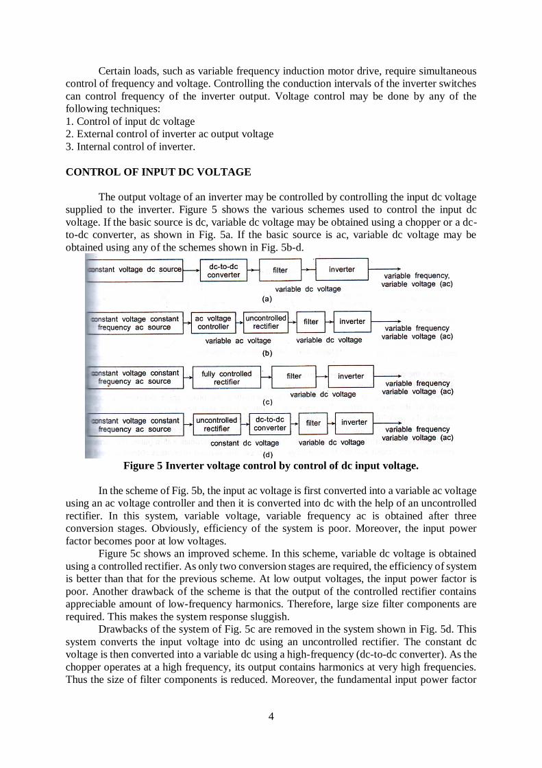
CONTROL OF INPUT DC VOLTAGE
The output voltage of an inverter may be controlled by controlling the input dc voltage
supplied to the inverter. Figure 5 shows the various schemes used to control the input dc
voltage. If the basic source is dc, variable dc voltage may be obtained using a chopper or a dc-
to-dc converter, as shown in Fig. 5a. If the basic source is ac, variable dc voltage may be
obtained using any of the schemes shown in Fig. 5b-d.
Figure 5 Inverter voltage control by control of dc input voltage.
In the scheme of Fig. 5b, the input ac voltage is first converted into a variable ac voltage
using an ac voltage controller and then it is converted into dc with the help of an uncontrolled
rectifier. In this system, variable voltage, variable frequency ac is obtained after three
conversion stages. Obviously, efficiency of the system is poor. Moreover, the input power
factor becomes poor at low voltages.
Figure 5c shows an improved scheme. In this scheme, variable dc voltage is obtained
using a controlled rectifier. As only two conversion stages are required, the efficiency of system
is better than that for the previous scheme. At low output voltages, the input power factor is
poor. Another drawback of the scheme is that the output of the controlled rectifier contains
appreciable amount of low-frequency harmonics. Therefore, large size filter components are
required. This makes the system response sluggish.
Drawbacks of the system of Fig. 5c are removed in the system shown in Fig. 5d. This
system converts the input voltage into dc using an uncontrolled rectifier. The constant dc
voltage is then converted into a variable dc using a high-frequency (dc-to-dc converter). As the
chopper operates at a high frequency, its output contains harmonics at very high frequencies.
Thus the size of filter components is reduced. Moreover, the fundamental input power factor

5
remains unity under all conditions of operation. However, losses in the system increase due to
use of an additional converter.
EXTERNAL CONTROL OF AC OUTPUT VOLTAGE
The constant ac output voltage (rms) from an inverter may be controlled using an ac
regulator (ac phase control). This method introduces a large harmonic content in the output
voltage. Moreover, the method can be used only for small power applications.
Figure 6 Series-connected inverters.
For high-power applications, two square-wave inverters may be connected in series to
variable ac voltage, as shown in Fig. 6. The output voltages of the inverter I and inverter II are
given to the primaries of the two transformers, whose secondary windings are connected in
series. The output voltages of the two transformers, v01 and v02 have same magnitude. The
phase angle between v01 and v02 , , can be controlled by controlling the phase angle between
the control signals of the two inverters. The resultant output voltage (v0) has a constant
magnitude 2V (double the peak of v01 and v02) and a variable pulse width, π-, as shown in Fig.
7. By varying from 0 to π, the width of output pulses may be varied from π to 0 and hence
the output voltage may be controlled from 2V to zero. At low voltages, it becomes a thin pulse,
the harmonic contents in the output voltage become large. Therefore, this method of voltage
control is used for voltage control (lower side) up to 25 to 30 per cent of the rated voltage.
Figure 7 Waveforms of series-connected inverters.
INTERNAL CONTROL OF INVERTERS
In this technique, the voltage control is obtained within the inverter. The output of the
inverter is in the form of a pulse width modulated wave. Controlling the width of output pulses,
controls the output voltage. This method not only provides variable output voltage but also
6
eliminates certain low frequency harmonics, which are responsible for poor performance. This
method is therefore, the most popular method of voltage control of inverter. Depending on the
required range of voltage control and required performance, a suitable PWM technique may be
used.
PULSE-WIDTH MODULATED INVERTERS
The square-wave inverters, suffer from two major drawbacks:
1. For fixed-source voltage, the output voltage of the inverter cannot be controlled. To achieve
voltage control, the inverter must be fed either from a controlled ac-dc or dc-dc converter.
2. The output voltage contains appreciable harmonics (low-frequency range). THD is also very
high (48.34%).
To achieve voltage control within the inverter and to reduce the harmonic contents in
the output voltage, pulse-width modulated (PWM) inverters are used. In PWM inverters,
widths of output pulses are modulated to achieve the voltage control. Among the large number
modulation techniques, simple modulation techniques are:
(a) Single pulse-width modulation (SPWM)
(b) Multiple or uniform pulse-width modulation (UPWM)
(c) Sinusoidal pulse-width modulation (sin-PWM).
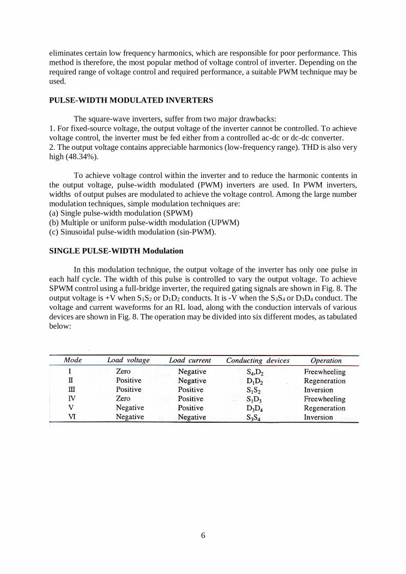
SINGLE PULSE-WIDTH Modulation
In this modulation technique, the output voltage of the inverter has only one pulse in
each half cycle. The width of this pulse is controlled to vary the output voltage. To achieve
SPWM control using a full-bridge inverter, the required gating signals are shown in Fig. 8. The
output voltage is +V when S1S2 or D1D2 conducts. It is -V when the S3S4 or D3D4 conduct. The
voltage and current waveforms for an RL load, along with the conduction intervals of various
devices are shown in Fig. 8. The operation may be divided into six different modes, as tabulated
below:

7
Figure 8 Gating signals, voltage and current waveforms of an SPWM inverter.
The width of output pulses (W) and the delay angle () of the gating signal IG1 may
related as W = π– 2. By controlling from zero to the width of output pulses may vary
from π to zero.
The rms value of the output voltage is given by
Thus the output voltage may be varied from 0 to V. by varying the pulse width from
zero to π. The output voltage waveform possesses odd- and half-wave symmetries. Therefore,
only odd b components shall be present in the Fourier-series expression, which are given by
Using (1) and (2), the output voltage may be written as
To eliminate the nth harmonic, sin (nW/2) = 0 or nW/2 = kπ. Therefore, W = 2kπ/n =
360k/n degree where k is an integer. For example, to eliminate the third harmonic, the required
pulse width W = 360/3 = 120°. Similarly, to eliminate the fifth harmonic, W = 360/5 = 72° or
W = 144°.
The variations of different harmonic components, the fundamental component and the
rms output voltage with the pulse width are shown in Fig. 9, as a ratio of the source voltage.
1
2

8
Figure 9 Harmonic profile of single PWM inverter.
The variations in the total harmonic distortion (THD) and the distortion factor (DF) are
also shown in the same figure. It may be observed that DF is minimum for the pulse width
around 120°. For smaller pulse widths or lower values of rms voltages, the harmonic contents
are comparable to the fundamental, resulting in very high values of THD and DF. Therefore,
single PWM technique can only be used to control the output voltage within a narrow range.
UNIFORM PULSE-WIDTH MODULATION
In a uniform PWM inverter, the output voltage has several pulses of equal width in each
half-cycle. The gating signals may be obtained by comparing a square-wave reference signal
with a high-frequency triangular carrier wave as shown in Fig. 10.
Figure 10 Generation of gating signals and output voltage waveforms of an UPWM
inverter.
The number of output pulses in each half-cycle may be obtained as
where fc and fref are the frequencies of carrier signal and reference signal, respectively,
and mf is the frequency modulation ratio.
The ratio of the amplitudes of the carrier signal (Ac) and the reference signal (Aref) is
called the amplitude modulation ratio or modulation index (ma). Mathematically,

9
The rms value of the output voltage may be obtained as
where W is the width of each pulse. By varying the amplitude modulation ratio from 0
to 1, the width of output pulses can be varied from 0 to π/N and hence the output voltage may
be varied from 0 to V.
The output voltage may be expressed in Fourier series by evaluating various harmonic
components using a computer programme. The variations of different harmonic components,
THD and DF with amplitude modulation ratio are shown in Fig. 11. It may be observed that
for lower values of ma, THD becomes very high. However, DF remains almost constant at
around 3.5% in the whole range of ma. This modulation technique can therefore be used for
voltage variation over a wide range.
Figure 11 Harmonic profile of UPWM inverter.
SINUSOIDAL PULSE-WIDTH Modulation
In sinusoidal pulse-width modulation technique, the width of output pulses is not
constant as compared to uniform PWM technique. Here the width of pulses varies in proportion
to the magnitude of a sine wave. This is achieved by comparing a sinusoidal reference signal,
vref of desired frequency with a high-frequency triangular carrier wave (vc). Two types of
switching schemes, bipolar switching scheme and unipolar switching scheme, are normally
used.
BIPOLAR SWITCHING SCHEMES
In bipolar switching scheme, the switches of the full bridge inverter is operated as
follows:
Figure12 Circuit diagram of single phase full bridge inverter
10
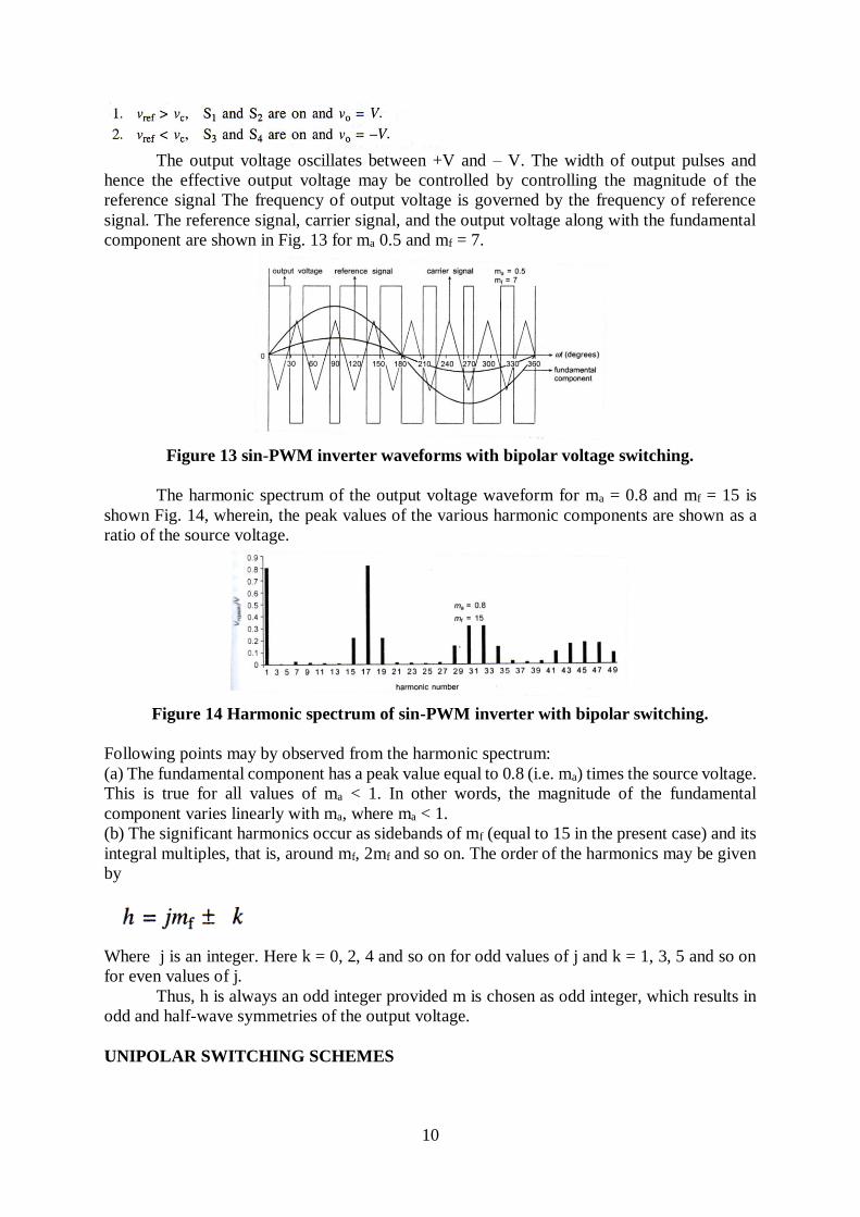
The output voltage oscillates between +V and – V. The width of output pulses and
hence the effective output voltage may be controlled by controlling the magnitude of the
reference signal The frequency of output voltage is governed by the frequency of reference
signal. The reference signal, carrier signal, and the output voltage along with the fundamental
component are shown in Fig. 13 for ma 0.5 and mf = 7.
Figure 13 sin-PWM inverter waveforms with bipolar voltage switching.
The harmonic spectrum of the output voltage waveform for ma = 0.8 and mf = 15 is
shown Fig. 14, wherein, the peak values of the various harmonic components are shown as a
ratio of the source voltage.
Figure 14 Harmonic spectrum of sin-PWM inverter with bipolar switching.
Following points may by observed from the harmonic spectrum:
(a) The fundamental component has a peak value equal to 0.8 (i.e. ma) times the source voltage.
This is true for all values of ma < 1. In other words, the magnitude of the fundamental
component varies linearly with ma, where ma < 1.
(b) The significant harmonics occur as sidebands of mf (equal to 15 in the present case) and its
integral multiples, that is, around mf, 2mf and so on. The order of the harmonics may be given
by
Where j is an integer. Here k = 0, 2, 4 and so on for odd values of j and k = 1, 3, 5 and so on
for even values of j.
Thus, h is always an odd integer provided m is chosen as odd integer, which results in
odd and half-wave symmetries of the output voltage.
UNIPOLAR SWITCHING SCHEMES

11
In unipolar switching scheme, the switch pairs S1S2 and S3S4 of the full-bridge inverter
of Fig. 12 are not operated as pair. Instead, the switches of the first leg, i.e. S1 and S4 are
operated by comparing the triangular carrier wave (vc) with the sinusoidal reference signal (vref)
The switches of the other leg, i.e. S2 and S3 are operated by comparing vc with -vref Following
logic is used to operate these switches:
The different possible combinations of on-state switches and corresponding voltages
are listed as follows:
Here VAN and VBN, are the potentials of the load terminals A and B, with respect to the
reference point N. The waveforms for the unipolar switching scheme, for mf = 12 and ma= 0.8,
are shown in Fig. 14. It may be observed that the output voltage fluctuates from 0 to +V in the
positive half-cycle and from 0 to -V in the negative half-cycle. This scheme is therefore called
unipolar switching scheme. The output voltage waveform possesses half wave and odd
symmetries. This will happen only if mf is chosen to be an even integer (mf should be odd in
bipolar switching)
Figure 14 Waveforms for unipolar voltage switching scheme.
The harmonic spectrum of the output voltage waveform is shown in Fig. 15. Following
points may be observed from the harmonic spectrum:

12
Figure 15 Harmonic spectrum of sin-PWM inverter with unipolar switching.
1. Like bipolar switching schemes, the fundamental component has a peak value equal to ma
times the source voltage. This is true for all values of ma between 0 and 1.
2. The harmonics occur as side bands of 2mf and its integral multiple. The advantage of unipolar
switching scheme over the bipolar switching scheme is that the frequencies of the harmonics
are doubled. This results in reduction in lower order harmonics. The order of the harmonics
can be given by
where j is an integer and k is an odd integer.
CURRENT SOURCE INVERTER
For the VSI, as the full form denotes, the output voltage is constant, with the output
current changing with the load − type, and/or the values of the components. But in the CSI, the
current is nearly constant. The voltage changes here, as the load is changed. In an Induction
motor, the developed torque changes with the change in the load torque, the speed being
constant, with no acceleration/deceleration. The input current in the motor also changes, with
the input voltage being constant. So, the CSI, where current, but not the voltage, is the main
point of interest, is used to drive such motors, with the load torque changing.
Single-phase Current Source Inverter (ASCI)
Figure 16 Single phase current source inverter (CSI) of ASCI type
The circuit of a Single-phase Current Source Inverter (CSI) is shown in Fig. 16. The
type of operation is termed as Auto-Sequential Commutated Inverter (ASCI). A constant
current source is assumed here, which may be realized by using an inductance of suitable value,
which must be high, in series with the current limited dc voltage source. The thyristor pairs,

13
Th1
& Th3, and Th
2 & Th
4, are alternatively turned ON to obtain a nearly square wave current
waveform. Two commutating capacitors − C1
in the upper half, and C2
in the lower half, are
used. Four diodes, D1–D
4 are connected in series with each thyristor to prevent the commutating
capacitors from discharging into the load. The output frequency of the inverter is controlled in
the usual way, i.e., by varying the half time period, (T/2), at which the thyristors in pair are
triggered by pulses being fed to the respective gates by the control circuit, to turn them ON, as
can be observed from the waveforms (Fig. 17). The inductance (L) is taken as the load in this
case, the reason(s) for which need not be stated, being well known. The operation is explained
by two modes.
Mode I: The circuit for this mode is shown in Fig. 18a. The following are the assumptions.
Starting from the instant,t = 0- , the thyristor pair, Th2 & Th
4, is conducting (ON), and the
current (I) flows through the path, Th2, D
2, load (L), D
4, Th
4, and source, I. The commutating
capacitors are initially charged equally with the polarity as given, i.e., . This
mans that both capacitors have right hand plate positive and left hand plate negative. If two
capacitors are not charged initially, they have to pre-charged.
At time, t = 0, thyristor pair, Th1
& Th3, is triggered by pulses at the gates. The
conducting thyristor pair, Th2 & Th
4, is turned OFF by application of reverse capacitor voltages.
Now, thyristor pair, Th1
& Th3, conducts current (I). The current path is through Th
1, C
1, D
2,
L, D4, C
2, Th
3, and source, I. Both capacitors will now begin charging linearly from (-Vco) by
the constant current, I. The diodes, D2 & D
4, remain reverse biased initially. The voltage,VD1
across D1, when it is forward biased, is obtained by going through the closed path, abcda as It
may be noted the voltage across load inductance, L is zero (0), as the current, I is constant. So,
As the capacitor gets charged, the voltage across VD1, increases linearly. At some time,
say t1, the reverse bias across D
1 becomes zero (0), the diode, D
1.starts conducting. An identical
equation can be formed for diode, D3 also. Actually, both diodes, D
1 & D
3, start conducting at
the same instant, t1. The time t
1 for which the diodes, D
1 & D
3, remain reverse biased is obtained
by equating,
.
The time is given by,
.
The capacitor voltages , appear as reverse voltage across the thyristors,
Th4& Th
2, when the thyristors, Th
1 & Th
3, are triggered. The value of is vc is
which, if computed at t = t1, comes out as,
using the value of t
1 obtained earlier. This means that the voltages across C
1 & C
2, varies
linearly from -Vco to zero in time t1. Mode I ends, when t = t1 and Vc = 0. Note that t
1 is the
circuit turn-off time for the thyristors.

14
Mode II: The circuit for this mode is shown in Fig. 18b. Diodes, D2
& D4, are already
conducting, but at , t = t1 diodes, D1 & D
3, get forward biased, and start conducting. Thus, at
the end of time t1, all four diodes, D
1–D
4 conduct. As a result, the commutating capacitors now
get connected in parallel with the load (L). For simplicity in analysis, the circuit is redrawn as
shown in Fig. 18c, where the equivalent capacitor is C/2 as C1 = C2 = C.
The equation for the current at the node is, where
The voltage balance equation is,
The solution of the equation is,
The initial conditions at t = 0 are, i0= I and . It should be noted that the
time, t is measured from the instant, the diodes, D1 & D
3, start coducting, i.e., from the instant,
mode I is over. Using the initial conditions stated earlier, the current is,
The capacitor current is .
The voltage across capacitor is,
This expression can also be obtained as,
where, as can be derived using
So, the above expressions are same, and can be written as,
substituting the expression for 0ωin any of the above expressions. So,
and
in the interval
As the current, tends to reverse, diode D3 prevents its reversal. Similarly, the diode,
D4
prevents the reversal of the current, . From the initiation of mode II, a time, t2 must
elapse for the current, to become zero (0). The time, t2 is,

15
as using,
.
The capacitor voltage at time t2,
Note that this is also the maximum value. Now, the load current is,
This shows that the load current has reversed from +I to –I during mode II, after time, t2. It is
also seen that the capacitor voltage changes by during each
commutation interval. The time t1, after substituting , comes out as,
The total commutation interval is,
Figure 17 Voltage and current waveforms

16
Figure 18 a) Mode I (1 phase CSI) b) Mode II (1-phase CSI)
c) Equivalent circuit for mode II
At the end of the process, constant current flows in the path, Th1, D
1, load (L), D
3, Th
3,
and source, I. This continues till the next commutation process is initiated by the triggering of
the thyristor pair, Th2
& Th4. The complete commutation process is summarized here. The
process (mode I) starts with the triggering of the thyristor pair, Th1 & Th
3. Earlier, the thyristor
pair, Th2
& Th4
were conducting. With the two commutating capacitors charged earlier with
the polarity as shown (Fig. 18a), the conducting thyristor pair, Th2
& Th4
turns off by the
application of reverse voltage. Then, the voltages across the capacitors decrease to zero at time
t1, (end of mode I), as constant (source) current, I flows in the opposite direction. Mode II now
starts (Fig. 18b), as the diodes, D1 & D
3, get forward biased, and start conducting. So, all four
diodes D1-D
4, conduct, and the load inductance, L is now connected in parallel with the two
commutating capacitors. The current in the load reverses to the value –I, after time t2, (end of
mode II), and the two capacitors also are charged to the same voltage in the reverse direction,
the magnitude remaining same, as it was before the start of the process of commutation (t = 0).
It may be noted that the constant current, I flows in the direction as shown, a part of which
flows in the two capacitors.

17