universidade tecnica de lisboa - … · universidade tecnica de lisboa instituto superior tecnico...
TRANSCRIPT
Departamento
de Engenharia
Informatica
UNIVERSIDADE TECNICA DE LISBOA
INSTITUTO SUPERIOR TECNICO
Architectures for Embedded Computing
MEIC-A, MEIC-T, MERC
Lecture Slides
Version 3.0 - English
Lecture 16
Title: Primary Memory - Technology, Organization and Memory Planes
Summary: Technologies; DRAMmemories operation; Memory planes; Primary mem-ory access optimization.
2010/2011
Primary Memory: Technology,Organization and Memory Planes
Prof. Nuno Roma ACE 2010/11 - DEI-IST 1 / 34
Architectures for EmbeddedComputing
Previous Class
Primary Memory
Primary MemoryTechnologies
Memory Planes
Primary MemoryAccess Optimization
Prof. Nuno Roma ACE 2010/11 - DEI-IST 2 / 34
In the previous class...
� Code optimization:
◮ Data access;
◮ Program access;
� Reduction of miss penalty with parallel techniques:
◮ Pre-Fetching;
◮ Non-blocking caches.

Road Map
Primary Memory
Primary MemoryTechnologies
Memory Planes
Primary MemoryAccess Optimization
Prof. Nuno Roma ACE 2010/11 - DEI-IST 3 / 34
Summary
Primary Memory
Primary MemoryTechnologies
Memory Planes
Primary MemoryAccess Optimization
Prof. Nuno Roma ACE 2010/11 - DEI-IST 4 / 34
Today:
� Primary Memory:
◮ Technologies;
◮ DRAM memories operation;
◮ Memory planes;
◮ Primary memory access optimization.
Bibliography:
• Computer Architecture: a Quantitative Approach, Section 5.3
Primary Memory
Primary Memory
Primary MemoryTechnologies
Memory Planes
Primary MemoryAccess Optimization
Prof. Nuno Roma ACE 2010/11 - DEI-IST 5 / 34
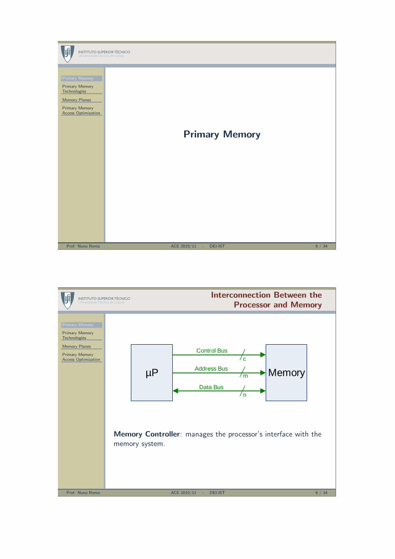
Interconnection Between theProcessor and Memory
Primary Memory
Primary MemoryTechnologies
Memory Planes
Primary MemoryAccess Optimization
Prof. Nuno Roma ACE 2010/11 - DEI-IST 6 / 34
µP MemoryData Bus
Address Bus
Control Busc
m
n
Memory Controller: manages the processor’s interface with thememory system.
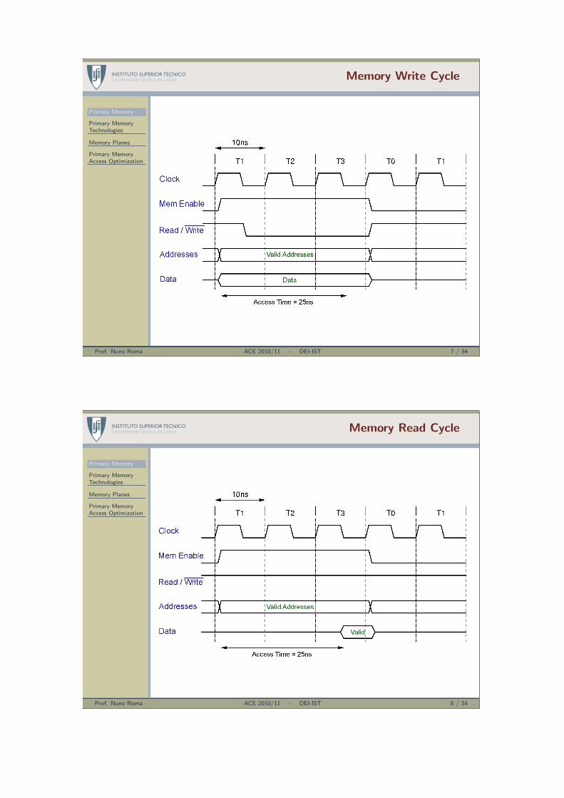
Memory Write Cycle
Primary Memory
Primary MemoryTechnologies
Memory Planes
Primary MemoryAccess Optimization
Prof. Nuno Roma ACE 2010/11 - DEI-IST 7 / 34
Memory Read Cycle
Primary Memory
Primary MemoryTechnologies
Memory Planes
Primary MemoryAccess Optimization
Prof. Nuno Roma ACE 2010/11 - DEI-IST 8 / 34

Access and Cycle Time
Primary Memory
Primary MemoryTechnologies
Memory Planes
Primary MemoryAccess Optimization
Prof. Nuno Roma ACE 2010/11 - DEI-IST 9 / 34
Access time: amount of time between a read/write requestand the instant when the requested word is read/written.
Cycle time: minimum amount of time between twoconsecutive memory requests.
Primary Memory Technologies
Primary Memory
Primary MemoryTechnologies
Memory Planes
Primary MemoryAccess Optimization
Prof. Nuno Roma ACE 2010/11 - DEI-IST 10 / 34

Types of Memory
Primary Memory
Primary MemoryTechnologies
Memory Planes
Primary MemoryAccess Optimization
Prof. Nuno Roma ACE 2010/11 - DEI-IST 11 / 34
RAM: Random Access Memory
SRAM: static memory - 6 transistors per memory bit
◮ Advantage: fast and low consumption
DRAM: dynamic memory - 1 transistor per memory bit
◮ Advantage: capacity and cost
ROM: Read-Only Memory - 1 transistor per memory bit
◮ Advantage: non-volatile and cheap
Flash: Flash memory - 1 transistor per memory bit
◮ Advantage: non-volatile and writable
Types of Memory
Primary Memory
Primary MemoryTechnologies
Memory Planes
Primary MemoryAccess Optimization
Prof. Nuno Roma ACE 2010/11 - DEI-IST 12 / 34
Memory Price TimeRead Write Access
SRAM 12 1 1 1
DRAM 1 12 12 18
ROM 1 1 - 1
Flash 6 12 850 12/850
� When is DRAM used?
◮ When more memory is more important than bettermemory.

Types of Memory
Primary Memory
Primary MemoryTechnologies
Memory Planes
Primary MemoryAccess Optimization
Prof. Nuno Roma ACE 2010/11 - DEI-IST 13 / 34
Static RAM - SRAM:
� Implemented with only 6 transistors;
� The state is kept while the power supply is on;
� Very fast memory: usually adopted by L1 caches, directlycoupled with the processor.
Types of Memory
Primary Memory
Primary MemoryTechnologies
Memory Planes
Primary MemoryAccess Optimization
Prof. Nuno Roma ACE 2010/11 - DEI-IST 14 / 34
L1 cache, implemented with SRAM technology, directly coupledwith the processor.

Types of Memory
Primary Memory
Primary MemoryTechnologies
Memory Planes
Primary MemoryAccess Optimization
Prof. Nuno Roma ACE 2010/11 - DEI-IST 15 / 34
Dynamic RAM - DRAM:
� Implemented with only 1 transistor;
� Needs to be periodically refreshed (8-64ms);
� Slower read and write cycles than SRAM memories;
� Advantages:
◮ More regular and simple ⇒ Greater capacity;
◮ A lot cheaper!!!
DRAM Memory Structure
Primary Memory
Primary MemoryTechnologies
Memory Planes
Primary MemoryAccess Optimization
Prof. Nuno Roma ACE 2010/11 - DEI-IST 16 / 34
� Addresses are supplied in two halves:
◮ RAS, Row Access Strobe
◮ CAS, Column Access Strobe

DRAM Memory Structure
Primary Memory
Primary MemoryTechnologies
Memory Planes
Primary MemoryAccess Optimization
Prof. Nuno Roma ACE 2010/11 - DEI-IST 16 / 34
� Addresses are supplied in two halves:
◮ RAS, Row Access Strobe
◮ CAS, Column Access Strobe
� The memory cells are structured as an array (usually square);
� Sense Amplifier - distinguishes the logic level that is stored ineach cell.

DRAM Memories Refresh
Primary Memory
Primary MemoryTechnologies
Memory Planes
Primary MemoryAccess Optimization
Prof. Nuno Roma ACE 2010/11 - DEI-IST 17 / 34
� 1 transistor per memory bit:
◮ The saved value vanishes with time;
◮ A read operations clears the data;
DRAM Memories Refresh
Primary Memory
Primary MemoryTechnologies
Memory Planes
Primary MemoryAccess Optimization
Prof. Nuno Roma ACE 2010/11 - DEI-IST 17 / 34
� The capacitor discharging effect implies the usage ofrefreshing mechanisms:
◮ Periodically, row-by-row (typically, within each 8ms, < 5%);
◮ A read operation discharges C: it is necessary to refresh thememory cell after each read operation;
◮ During the refresh, it is not possible to access the memory.
⇒ Significant variations of the access/cycle times!⇒ Read and write cycles are slower than in SRAM
memories.
DRAM Access
Primary Memory
Primary MemoryTechnologies
Memory Planes
Primary MemoryAccess Optimization
Prof. Nuno Roma ACE 2010/11 - DEI-IST 18 / 34
� Cell selection:
◮ RAS:Row Address Selection
◮ CAS:Column Address Selection
� Multiplexed address lines: RAS + CAS
� There is little to do, in what concerns the latencyAlternative: improve the throughput
Fast Page Mode: keeps the row address and changes the columnaddress (Extended Data Output (EDO) DRAM is anoptimization of this mode).

Synchronous DRAM (SDRAM)
Primary Memory
Primary MemoryTechnologies
Memory Planes
Primary MemoryAccess Optimization
Prof. Nuno Roma ACE 2010/11 - DEI-IST 19 / 34
Synchronous DRAM (SDRAM):
� Synchronous access to the memory, i.e., the memoryexecutes operations synchronously with a clock signal (e.g.PC133), allowing a pipeline operation, i.e., an operationcan be started before the previous one has finished.
� Data bus with 8 bytes (64 bits) width.
Synchronous DRAM (SDRAM)
Primary Memory
Primary MemoryTechnologies
Memory Planes
Primary MemoryAccess Optimization
Prof. Nuno Roma ACE 2010/11 - DEI-IST 20 / 34
Access cycle:
tRCD - RAS to CAS delay
CL - CAS latency
� Allows reading 2, 4 or 8 words in a single read operation,without needing to repeat the RAS/CAS sequence;
� Allows reading other columns (different CAS) of the samerow (equal RAS).
Technology Evolution of SDRAM Memories
Primary Memory
Primary MemoryTechnologies
Memory Planes
Primary MemoryAccess Optimization
Prof. Nuno Roma ACE 2010/11 - DEI-IST 21 / 34
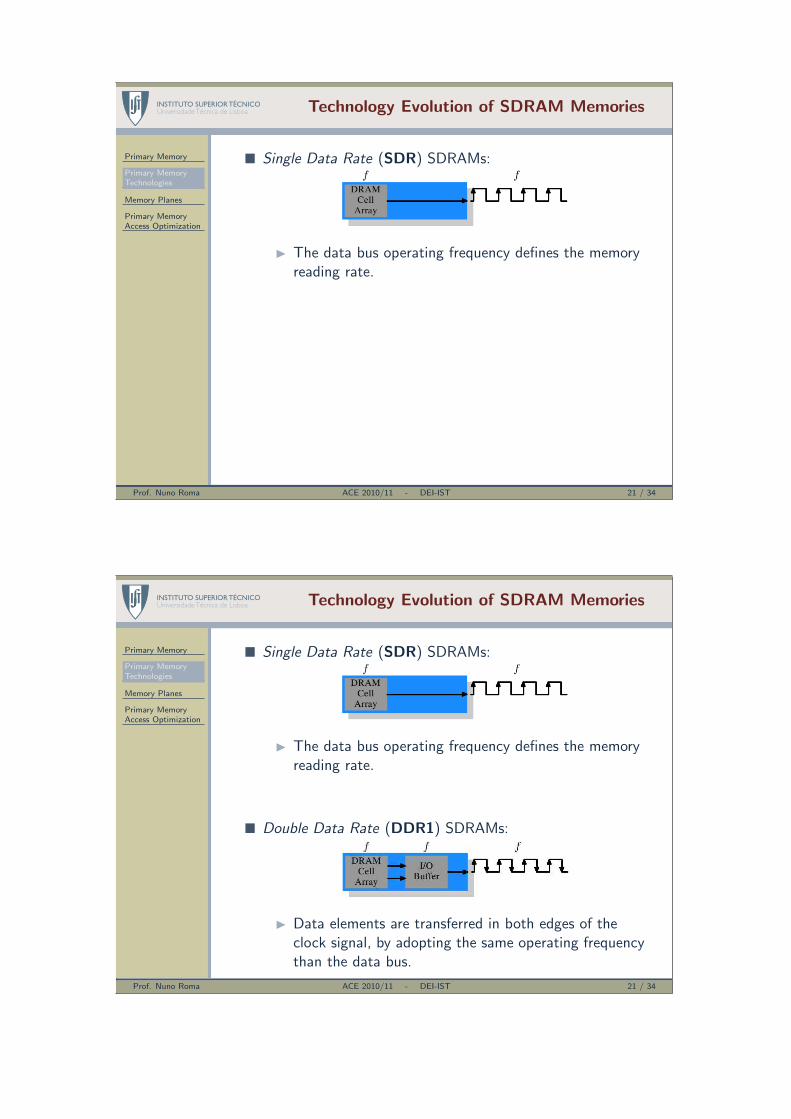
� Single Data Rate (SDR) SDRAMs:
◮ The data bus operating frequency defines the memoryreading rate.
Technology Evolution of SDRAM Memories
Primary Memory
Primary MemoryTechnologies
Memory Planes
Primary MemoryAccess Optimization
Prof. Nuno Roma ACE 2010/11 - DEI-IST 21 / 34
� Single Data Rate (SDR) SDRAMs:
◮ The data bus operating frequency defines the memoryreading rate.
� Double Data Rate (DDR1) SDRAMs:
◮ Data elements are transferred in both edges of theclock signal, by adopting the same operating frequencythan the data bus.

Technology Evolution of SDRAM Memories
Primary Memory
Primary MemoryTechnologies
Memory Planes
Primary MemoryAccess Optimization
Prof. Nuno Roma ACE 2010/11 - DEI-IST 22 / 34
� DDR2 SDRAMs:
◮ The data bus operating frequency is doubled, and thedata elements are transferred in both edges of theclock signal.
� DDR3 SDRAMs:
◮ The data bus operating frequency is four times faster,and the data elements are transferred in both edges ofthe clock signal.

SDRAM Memory Nomenclature
Primary Memory
Primary MemoryTechnologies
Memory Planes
Primary MemoryAccess Optimization
Prof. Nuno Roma ACE 2010/11 - DEI-IST 23 / 34
Example: DDR2-667
Clock Rate = 333 MHz
Transfer Rate = Clock Rate×2 = 667 Mega transfers per second
Bandwidth = 8 Bytes× Transfer Rate = 5336 MB/sec
DIMM name = PC5300
Other Memories: FLASH Memory
Primary Memory
Primary MemoryTechnologies
Memory Planes
Primary MemoryAccess Optimization
Prof. Nuno Roma ACE 2010/11 - DEI-IST 24 / 34
� Non-volatile memory: does not need a power supply to keep itscontents;
� Based on the same technology as EEPROMs;
� Can be erased and re-written multiple times;
� Relatively high access times (when compared with DDR SDRAM).

Other Memories: Solid State Disk (SSD)
Primary Memory
Primary MemoryTechnologies
Memory Planes
Primary MemoryAccess Optimization
Prof. Nuno Roma ACE 2010/11 - DEI-IST 25 / 34
� Non-volatile;
� Based on FLASH or SDRAM (with battery) memories;
� Have been replacing the magnetic discs;
� Mechanically much more resistant;
� Greater access times than SDRAM, but much smaller than aHDD.
Memory Planes
Primary Memory
Primary MemoryTechnologies
Memory Planes
Primary MemoryAccess Optimization
Prof. Nuno Roma ACE 2010/11 - DEI-IST 26 / 34
Memory Planes
Primary Memory
Primary MemoryTechnologies
Memory Planes
Primary MemoryAccess Optimization
Prof. Nuno Roma ACE 2010/11 - DEI-IST 27 / 34
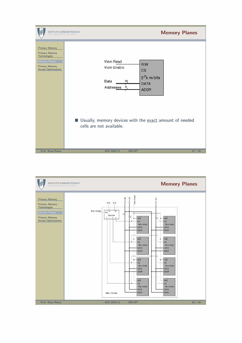
� Usually, memory devices with the exact amount of neededcells are not available.
Memory Planes
Primary Memory
Primary MemoryTechnologies
Memory Planes
Primary MemoryAccess Optimization
Prof. Nuno Roma ACE 2010/11 - DEI-IST 28 / 34
Memory Planes
Primary Memory
Primary MemoryTechnologies
Memory Planes
Primary MemoryAccess Optimization
Prof. Nuno Roma ACE 2010/11 - DEI-IST 29 / 34
Example:
00000h
07FFFh
10000h
1FFFFh
F0000h
FFFFFh
RAM
ROM
...
...
RAM
Primary Memory Access Optimization
Primary Memory
Primary MemoryTechnologies
Memory Planes
Primary MemoryAccess Optimization
Next Class
Prof. Nuno Roma ACE 2010/11 - DEI-IST 30 / 34

Cache-Memory Interconnect Optimization
Primary Memory
Primary MemoryTechnologies
Memory Planes
Primary MemoryAccess Optimization
Next Class
Prof. Nuno Roma ACE 2010/11 - DEI-IST 31 / 34
� The processor is connected to the memory using a bus;
Cache-Memory Interconnect Optimization
Primary Memory
Primary MemoryTechnologies
Memory Planes
Primary MemoryAccess Optimization
Next Class
Prof. Nuno Roma ACE 2010/11 - DEI-IST 31 / 34
� The processor is connected to the memory using a bus;
� The bus clock frequency is usually much lower than theprocessor internal operating frequency (about 10 times);⇒ Increase of the miss penalty!!!
� Memory access cycle example:
◮ 1 clock cycle to send the address;
◮ 15 clock cycles to start each DRAM access;
◮ 1 clock cycle to send each word from memory.
Considering a cache with 4 words per block, the miss penalty isgiven by:
tp = 1 + 4× 15 + 4× 1 = 65 bus cycles.
� Alternatives:
◮ Wider bus to connect the memory;
◮ Interleaved memory banks.

Cache-Memory Interconnect Optimization
Primary Memory
Primary MemoryTechnologies
Memory Planes
Primary MemoryAccess Optimization
Next Class
Prof. Nuno Roma ACE 2010/11 - DEI-IST 32 / 34
Alternatives:
◮ Simple bus to connect the memory (1 word);
◮ Wider bus to connect the memory (several words);
◮ Interleaved memory banks.
Next Class
Primary Memory
Primary MemoryTechnologies
Memory Planes
Primary MemoryAccess Optimization
Next Class
Prof. Nuno Roma ACE 2010/11 - DEI-IST 33 / 34

Next Class
Primary Memory
Primary MemoryTechnologies
Memory Planes
Primary MemoryAccess Optimization
Next Class
Prof. Nuno Roma ACE 2010/11 - DEI-IST 34 / 34
� Virtual Memory:
◮ Advantages of secondary memory;
◮ Segments vs Pages;
◮ Address translation:
• Hierarchy tables;
• Inverted tables.