universiti putra malaysia design and simulation of...
TRANSCRIPT
UNIVERSITI PUTRA MALAYSIA
DESIGN AND SIMULATION OF 10 kHz VOLTAGE-SOURCE THREE- PHASE RESONANT DC-LINK INVERTER FOR 10 kW OHMIC
HEATING PROCESS
ELSADIG MOHAMED ALI
FK 2001 43
DESIGN AND SIMULATION OF 10 kHz VOLTAGUKlURCE THREEPHASE RESONANT DC-LINK INVERTER FOR 10 kW OHMIC HEATING
PROCESS
By
ELSADIG· MOHAMED ALI
Thesis Submitted in Fulfilment of the Requirement for the Degree of Master of Science in the Faculty of EDgineering
Univeniti Putra Malaysia
May 2001

6ft,u,�itv�fo, .ily�
.ily��� .ily�ruut� 6� 60f10/ruut�
ii

Abstract of thesis presented to the Senate of Universiti Putra Malaysia in fulfilment of the requirement for the degree of Master of Science
DESIGN AND SIMULATION OF 10 kHz VOLTAGE-SOURCE THREE-
PHASE RESONANT DC-LINK INVERTER FOR 10 kW OHMIC HEATING
PROCESS
BY
ELSADIG MOHAMED ALI
May 2001
Chairman: Associate Professor Norman Bin Mariun, Ph. D.
Faculty: Engineering
There has been much interest recently in heat processing and packing for rapid heating
and non-thermal microbial inactivation of food. Ohmic heating is one of the new
technologies used. It is an operation in which heat is internally generated within foods
due to the passage of alternating electrical current. Much of the research carried out on
ohmic heating to date has been done using frequency of 60 and 50 Hz. Low frequency
has an electrolytic effect similar, though to a lesser extent to that of direct current. The
major electrolytic effect is the dissolution of the metallic electrodes, which may
contaminate the product.
iii

One of the most effective methods utilised to overcome the electrolytic effect, and
give high perfonnance of ohmic heating is high frequency resonant converter. The
literature review includes resonant DC-link inverter, three-phase sinusoidal PWM
inverter, control of the inverter, filters design, ohmic heating, and power MOSFET.
Sinusoidal pulse width modulation was used to produce pure sinusoidal current at high
frequency and low hannonics. Although it had drawbacks such as suffering high stress
and losses during switching these effects were reduced by soft switching, where the
MOSFET is switched on at zero voltage (ZVS). Power MOSFET was chosen for high
switching device, low resistance and feature suitable for static power converter.
The study presented the design for 10 kHz of voltage-source resonant DC-link inverter
involving the design of three-phase rectifier, filter, resonant circuit, sinusoidal PWM
inverter and control circuit. The perfonnance of three-phase resonant dc-link inverter
was simulated based on the design parameters. Three-phase sinusoidal output current
at 10 kHz was produced, which is suitable for driving AC resistive load (ohmic
heating).
iv

Abstrak tesis untuk dikemukakan kepada Senat Univecslu Putra Malaysia sebagal memenuhi keperluan bagi ijazah Master Sains
REKABENTUK DAN SIMULASI PENUKAR SUMBER VOLTAN RESONAN TIGA FASA HUBUNGAN DC UNTUK PROSES PEMANASAN OHMIK PADA
lOkW
Oleh
ELSADIG MOHAMED ALI
MeilOOl
Pengerusi: Profesor Madya Norman Bin Marion, Ph. D.
Fakulti: Kejuruteraan
Terdapat begitu banyak minat sejak akhir-akhir ini dalam pemprosesan dan
pembungkusan haba untuk pemanasan segera dan penyahaktif mikrobial bukan terma
bagi makanan. Pemanasan ohmik adalah salah satu temologi barn yang digunakan. Ia
adalah satu operasi di mana haba dijana secara dalaman di dalam makanan disebabkan
oleh pengaliran arus elektrik ulang alik. Banyak penyelidikan dijalankan terhadap
pemanasan haba sehingga hari ini dengan menggunakan frekuensi pada 60 dan 50 Hz.
Frekuensi rendah mengandungi kesan elektrolitik, walaupun berlrurangan kesannya
berbanding dengan penggunaan arus terus. Kesan elektrolitik utama ialah pencairan
elektrod metaliIc, yang mungkin mencemari produk.
Satu daripada kaedah paling efektif yang digunakan untuk mengatasi kesan
elektrolitik. dan memberikan prestasi pemanasan ohmik yang tinggi ialah dengan
v
menggunakan penukar resonan berfrekuensi tinggi. Kajian penulisan merangkumi
penukar resonan hubungan DC, penukar PWM bentuk sinus tiga fasa, kawalan bagi
penukar, rekabentuk penapis, pemanasan ohmik, dan MOSFET kuasa.
Modulasi lebar denyut sinusoidal digunakan untuk menghasilkan arus bentuk sinus
yang tulen pada frekuensi tinggi dan harmonik rendah. Walaupun ia mempunyai
kelemahan seperti mengalami tekanan dan kehilangan kuasa yang tinggi sepanjang
pensuisan, kesan-kesan ini dapat dikurangkan dengan pensuisan lembut, di mana
MOSFET disuiskan pada voltan sifar. MOSFET kuasa telah dipilih kerana
keupayaannya sebagai peranti bersuis tinggi, rintangannya yang rendah dan
kesesuaian cirinya sebagai penukar kuasa statik.
Kajian ini menampilkan rekabentuk penukar sumber voltan titi penuh resonan
hubungan DC pada 10 kHz yang mengandungi rekabentuk bagi penerus masukan tiga
fasa, penapis, litar resonan, penukar PWM bentuk sinus dan litar kawalan.
Kemampuan penukar resonan tiga fasa hubungan de disimulasikan merujuk kepada
parameter-parameter yang direkabentuk. Arus keluaran bentuk sinus tiga fasa pada 10
kHz dihasilkan, yang mana bersesuaian untuk memacu beban rintangan AC
(pemanasan ohmik).
vi

ACKNOWLEDGEMENTS
With hmnble gratitude, I wish to express thanks to Almighty Allah who has enabled
me to further my studies. Praises and thanks for His grace and strength that have
helped me to �sfully complete my project.
I would like to express my sincere thanks and gratitude to my' supervisor Associate
Professor, Dr. fr. Nonnan Bin Mariun, for his helpful supervision, suggestions,
encouragement and constant support throughout the period of study.
My gratitude is due to fr. Hishamuddin Bin Jamaludin and Dr. Sinan Mahmud Bashi,
members of the supervisory committee for their advices, ideas, support and c0-
operation in completing this report.
I am grateful to Dr. Ishak Aris and Dr. Nasrullah Khan for their knowledge, and
assistance they offered me during my period of study. I am also thankful to all
University Putra Malaysia staff, especially to Electrical and Electronics Engineering
fuculty and my colleagues for friendly environment and co-operation discussion.
VII
I certify that an Examination Committee met on 21th May 2001 to conduct the final examination of Elsadig Mohammed Ali on his Master of Science thesis entitled "Design and Simulation of 10 kHz Voltage-Source Three-Phase Resonant Inverter for 10 kW O hmic Heating Process" in accordance with Universiti Pertanian Malaysia (Higher Degree) Act 1980 and Universiti Pertanian Malaysia (Higher Degree) Regulation 1981. The Committee recommends that the candidate be awarded the relevant degree. Members of the Examination Committee are as follows:
Ishak Aris, Ph. D. Faculty of Engineering Universiti Putra Malaysia (Chairman)
Norman Bin Mariun, Ph. D. M.Eng. Associate Professor Faculty of Engineering
, Universiti Putra Malaysia (Member)
Hishamuddin Bin larnaludin Faculty of Engineering Universiti Putra Malaysia (Member)
Sinan Mahmud Bashi, Ph. D. Faculty of Engineering Universiti Putra Malaysia (Member)
-'
HAZALIMOHAYIDIN, Ph. D Professor! Deputy Dean of Graduate School, Universiti Putra Malaysia Date: 7 JUN ZOOl
viii

This thesis is submitted to the Senate of Universiti Putra Malaysia has been accepted as fulfilment of the requirement for the degree of Masters of Science.
ix
AINI IDERIS, Ph.D, Professor/ Dean of Graduate School, Universiti Putra Malaysia
Date: 1 4 JLJN 2001

DECLARATION.
I hereby declare that the thesis is based on my original work except for quotations and citations, which have been duly acknowledged. I also declare that it has not been previously or currently submitted for any other degree at UPM or other institutions.
ELSADIG MOHAMED ALI ELSHIEKIL
Date: ";f" 6 . z-.\
x

TABLE OF CONTENTS
Page DIDICATION ABSTRACT
ii iii
ABSTRAK ACKNOWLEDGEMENTS APPROVAL SHEEfS DECLARATION FORM liST OF FIGURES
v vii ix x
XlI XV liST OF ABBRVITIONS/GLOSSARY OF TERMS
CHAPTER
1 INTRODUCTION ............ ......... ............... ...... '" ... . . . . . . . .. ... . . . . . . 1 1 .1 Ohmic Heating............ . ..... ... ............ . .. ...... ...... ... .... ..... .. 1 1 .2 Resonant DC-Link Inverter ... ............. ... .. . . . . .. . ... . . . . .. ... .. . .... 2 1 .3 Objective of the Study....................... . ........... . ......... ... ..... 3 1.4 Thesis Layout............... ............ ............ .. .. . . ...... .. ... .... . . . 4
2 LITERATURE REVIEW............... ...... ... ...... ............... .. . ........ . .. 5 2 .1 Resonant OC-Link Inverter ......... .. . ... '" . . . . .. . .. . .. . .. ... . . .. ... .... 5
2 .1 .1 Main Advantages of the Voltage-Source Inverter... .. . ........ 6 2 .1 .2 Resonant OC-Link voltage-Source Inverter................ . 8
2.2 Voltage Control of the Inverter............ . . . . ..... . .. .................. 10 2 .2.1 Single Pulse Width Modulation ...... ... .. . ... .. .... ...... ..... 10 2 .2.2 Multiple Pulse Width Modulation...... ... ...... .. . ... ...... ..... 12 2 .2 .3 Sinusoidal Pulse Width Modulation.... .. . . . . .. .. . ... . .. ... .. . ... 13
2 .3 Three-Phase PWM Invertetr...... ...... . . .... ... ......... ...... ...... .... 14 2.3.1 The Square Wave PWM... ...... ... .. . . . . . . . ... .. . . . . . . . . .. ...... 15 2 .3 .2 The Sinusoidal PWM..... ... . ... . ........... ... . ........ ... .. . . . 16
2 .4 Power MOSFET...... ........................... ......... . ................. . 18 2 .4.1 Principle of Operation...... ..... . ...... . . .... . . .... ... ... ...... ... 19 2.4.2 Output Characteristic ... ............ ... ............ ...... .. ..... 22 2.4.3 Safe ()peration Area ............ . ... .. ..... . ... .. , ... ... ... ... ... ... 22 2 .4.4 Switching Characteristic .... .... . ... .. , ..................... '" .... 23 2.4.5 Heat Sink... ... ... ...... ...... ............ ............ ...... .......... 24 2.4.6 Gate Drive Circuits ......... ......... '" ...... .. , '" ... . . .... '" .. .. 26 2.4.7 Harmonics Filtering Design ... ...... ... ... ...... ............ ...... 27
2 .5 ()hmic Heating . .... . ............ .. .... ...... '" .. . .. . . . . . .. ... ... ... . .. . .... 28 2.5.1 Ohmic Heating Principles..... ... .... .. . . . . ...... ... ......... ..... 29 2.5 .2 Advantage of Ohmic Heating.............................. ...... 32 2.5.3 Design of the Ohmic Heater........ . ........................ ... .. 33 2 .5.4 Effect of Frequency.. .............................................. 34
2.6 Smnmary . ........ . . . '" ..... ........ ..... '" . .......... .. .... ......... , ... .... 35
Xl

3 METHOOOLOOY AND DESIGN ....... . ..... . ... . ... . . . . . .. , .. . . .. ... ... ... ... 36 3.1 Design of Voltage-Source Resonant DC-Unk Inverter... ... .. . . .. . . . 36
3.1.1 Input Rectifier... . . . .. . .. .... .. . ... .... . . ... ... ...... . . .... ........ 37 3.1 .2 Input Filter... . . ...... .. .. . . . ... ........ ... . ...... . . . ... . ..... ..... . . . 38 3.1 .3 Resonant DC-Link Circuit......... . . ...... ... . ..... .... . . .... . .. 39 3 .1.4 Sinusoidal PWM Inverter.... ....... . . .... ... . ..... .. ....... . . . ... 42 3 .1.5 Heat SinkI>esign...... ... .. . .. . ......... . ......... . . . ... ...... . ... . 43
3.2 Design of the Control Circuit... . .. . . ................... . ... . . .......... . . .. 45 3.2.1 The Function Generator ICL 8038... ... ... ... ... .. . ... ... ... .... 46 3.2.2 COIDparator..... . ... ...... ... ......... .. ........ ....... . . ........ . . . 48 3.2.3 D Flip-Flops IC74LSI74... ...... ..... . ..... . ... ... ........... ... 49 3.2.4 The IC 555 Timer.. . . . . . .. . . . ..... . .... .. .......... . . .. . . ... ........ 49 3.2.5 Gate Driver IC 00213...... ......... ............... . .. . . .... .... 51 3.2.6 Soft Switching... . . . ... . . . ... . . . ... . .. . . . .. .... ...... . .. . . . ... .... 52 3.2.7 High Voltage Three-Phase MOS Gate Oliver IR 2233...... 53
3.3 Simulation Circuits . . . . ...... ... ... . . . . . ......... . . .......... '" .... . , . . .... 53
4 RESULTS AND DISCUSSION ..... . ... ... ... . . . ........ .... . . . ...... ... ........ . 54 4 .1 lbree-Phase Rectifier...... ........... . ..... . . . .... . .. ...... . . . ... . . . . . . .... S4 4.2 The Comparator . . : ...... ...... . ,. ..... . ..... ... . ..... .. . .. .. . . . . . ... .... . . . S4 4.3 Resonant DC-Link Inverter. . . . ....... . ... . . . . . .... . .... ...... ... . ... ... . . S7 4.4 Three-Phase <>utput.. . ... . . . ... .. . . . . . . ... ........... ... . .. . . . . ... . . . ...... 59
5 CONCLUSION .... .. .. .......... . .. .. . ... . ..... ..... . . " ... . . . . .. . . . . . . . .. ... . .. . . . . . 61 5.1 Recommendations.... .. . . . .. . . . . ..... . .... . . . ........... .. . .. . . .... . .. . .. . ... 62
REFERENCES... .... . . . ... . . ...... . ... .. . ..... . .. ... .... . . . .. . .... . .. .. .... . . . .. . . . . . 63
APPENDICES. . . . . . .. . ..... . ......... . . .... . ..... ... .... ................ . . . . . ... . . .... 66 A Function Generator ICL8038 . .. . . . .. . . .... . . . . . .. .. . .. .... . . ... . . . ... . . ...... . . . .. 66 B MOSFET Gate Driver.... . . .......... . . ...... .... ......... . ..... . .... . .... ... .... ... . 75
BIODATA OF THE AUTHOR............................................................... .................. 97
xii

LIST OF FIGURES
Figure Page
Figure 2.1 V oltage-SOW'Ce resonant DC-link i nverter . . . . . , . . . . . . '" . .. . .. . . . . . . 7
Figure 2.2 Current-so urce resonant DC-link inverter . . . .. . . . . . . ..... .. '" . .. . . . 7
F igure 2.3 Resonant DC link inverter .. . . . . . . . . . . . . . . . . . . . . . . .. . . . . . .. .. . . . . . . . . . . 9
F igure 2 .4 Single pulse width modul ation . . . '" ... '" . . . . . . ... . . . .. , . .. . . . . .. . . .. 11
Figure 2 .5 Multiple pu lse width modulation . . . . . , . . . . . . .. . . . . . . . . . . . . . . .. . . . . . . . 11
Figu re 2 .6 S inusoidal pu lse width modul ati on . . . . .. . . . . . . . . . . .. .. . . . . . . . .. . .. . ... . 13
Figure 2 .7 Control circuit of square-wave PWM . .. . . .... .. . . . . . . . . .. .. . '" . . . . . 15
Figure 2.8 Voltage waveforms for three-ph ase squ are -wave PWM . . . ... . , . . 16
Figure 2 .9 V olmge wavefOlUlS for three-ph ase sinusoidal PWM.. . .. . . .. .. . . 17
Figure 2 .10 N -channel power MOSFET . .. . . .. ... . .. . , . .. . . , ... .. . .. . .. . . .. . . . . .. 21
Figure 2 .11 Power MOSFET cha ract eristic . .. '" . .. . .. . . . . ..... . .. .... ,. .. . . . ... 22
Figure 2 .12 WavefOIm ofpo wer M OSFET .. . ...... . .... .. . .. . .... .. . .. . . .. . . . .. 24
Figure 2 .13 Harmonics filtering des ign . . . . .. . . . . . , '" . . . '" . . . '" ., . . . . . . . .. .. .. 27
Figu re 2.14 Principle of ohmic he ater. . .. . . ... . . . .. . .. . . . .. . . . . . . . . .. . .. . ... .. . . . . 34
Figure 3.1 S ystem bl ock di agram .. . . . . ... . . . . . . . . . . ... . . . . . . . . . . . . . .. . .. . . . . . . . . . . . 37
Figure 3 .2 Reson ant wavefo rms and lin k s witch ML ... '" ... '" . ..... ... ...... ..... 40
Figure 3.3 Thermal resis tance rel ationship . . .. . . . .. . . . . , ......... , ... ...... ..... 44
Figure 3.4 The function generator ICLS038. . . . .. . .. . . . . . . ... . .. .. . ... . . . .. . . . . .. 47
Figure 3 .5 The comparator c ircuit . . . . . . . . . .. . . .. . .. . .. . . ... . . . . . . . . . . . . . . .. . . . . .. . 49
Figure 3.6 D flip -flops IC74LS I74.. . . . . . .. . . . ... ... . .. .. .. . . . . . . . .. . . . . . . .. . . . . .. 50
X11l

Figure 3.7 IC 555 timer . . . . . , '" ... . .. '" . . . '" .. . . . . . . . . . . . . . ... . . . . . , '" . .. . . . ... . 50
Figure 3.8 Gate driver IC IR 2213 .. . . .. . . . ... '" .. . . . . '" .. . ... '" .. . . . , .. . ... .. . . . . 52
Figure 4 .1 The output ofthree-phase rectifier..... . . . . . . . . . . .. . . . .. . . . . . . . . ... . . 55
Figure 4.2 View of the ripple voltage (less than 0.04). . . .. . . . . . . . . . . . ... . . . . . . 55
Figure 4.3 The output current of the rectifier.. . . . . . . . .. .. . . . . . . . . .. .. . .. . . . . . . . . . . 55
Figw'e 4.4 The comparator input and output. . . . ... . . . .. . . .. . . . . . . . .. . ... . . . . . . . . 56
Figure 4 .5 Six SPWM control signals.. . . .. . . . . .. . . . ... . . . . . .. . . . .. . .. ... . ... . . . . . . . 57
Figure 4.6 Waveforms of the capacitor and link sw itch. . . .... ... ... ... ...... ........ 58
Figure 4.7 View wllveforms of the capacitor and link switch.... ..... ... .. .... ..... 58
Figure 4.8 The line-to-l ine output voltage. .. . ... . . . . . .. . . . .. . . . . . .. . . . . . . . . . . .. . . 59
Figure 4 .9 View of the three-phase output current . . . . . . . . . . . . . . . . . .. . . .. ... . . . . 60
xiv
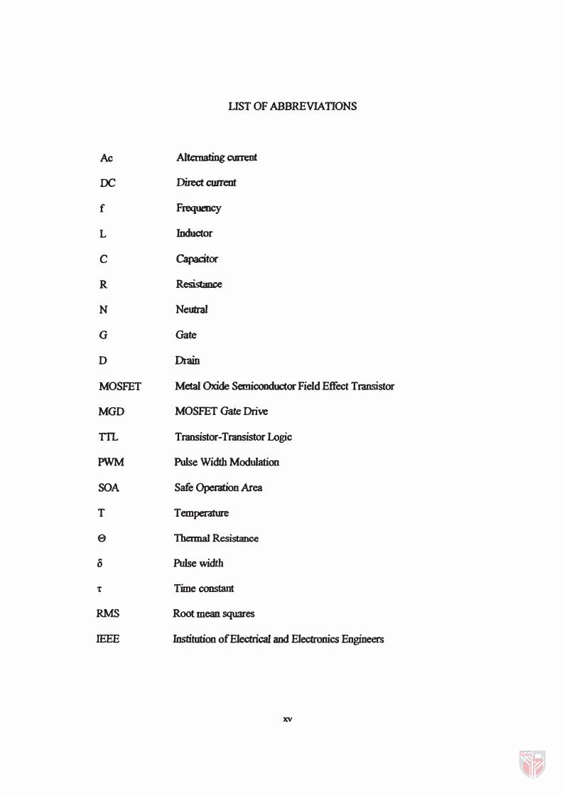
Ac
OC
f
L
C
R
N
G
D
MOSFET
MGD
TIL
PWM
SOA
T
e
o
T
RMS
IEEE
UST OF ABBREVIATIONS
Alternating current
Direct current
Frequency
Inductor
Capacitor
Resistance
Neutral
Gate
Drain
Metal Oxide Semiconductor Field Effect Transistor
MOSFET Gate Drive
Transistor-Transistor Logic
PuIse Width Modulation
Safe Operation Area
Temperature
Thennal Resistance
Pulse width
Time constant
Root mean squares
Institution of Electrical and Electronics Engineers
xv

ML MOSFET l ink switch
V GML MOSFET l ink switch gate drive
k Resonant inductor current
xvi

CHAPTER I
INTRODUCTION
There has been much recent interest in heat processing and aseptic packing for rapid
heating and non-thermal microbial inactivation of food. Among the new technologies
involved is ohmic heating.
1.1 Ohmic Heating
Ohmic heating is a process in which heat is generated within the food itself, from the
passage of an electric current. As the current passes through the food, heat is
generated from the resistance to its flow [1]. In most ohmic heating research, an
alternating current of low frequency (50 to 60 Hz) is used. However, a low frequency
current has an electrcJytic effect similar to that of direct current, though to lesser
extent. The major electrolytic effect is the dissolution the metallic electrodes, which
may contaminate the product [2].
One of the most effective methods to minimize the electrolysis is to use a high
frequency current from a resonant power inverter. The resonant inverter is a new
I
technology for producing a high frequency current to minimise the harmonics, noise
and switching loss in semiconductor devices.
For ohmic heating to be successful, the food must exhibit some electrical conductivity.
It is normally a unique value to the food and increases with the temperature.
However, in some food materials, it decreases instead [2].
2.1 Resonant DC-Link Inverter
Semiconductor power device consist of two different power losses, these are the
conducting, and the switching losses. The conducting losses depend on the
construction of the device and the switching losses depend on the voltage, current, and
switching frequency of the device.
The soft-switching power converter has been one of the fastest growing areas in power
electronics in the past several years. The resonant DC-link (RDCL) techniques
reduced the switching losses of the power device in the inverter virtually to zero
compared with hard-switching techniques. There are two types of RDCL soft
switching these are zero-voltage-switching (ZVS) and zero-current-switching (ZCS).
The voltage and current source RDCL can obtain nearly loss-less tum-ON and turn
OFF switching, thus increasing device switching frequencies of several order of
2

magnitude higher than that achievable in hard-switching converters. The power
device characterization and selection for the RDCL converters remain one of the
important issues.
Metal oxide semiconductor field effect transistor (MOSFET) was chosen due for its
high switching speed, low ON resistance and operating junction temperature to reduce
conduction loss and yield a high efficiency. The advantage of three-phase sinusoidal
pulse width modulation (PWM) is to produce pure sinusoidal output at high frequency,
reduced filter requirements for harmonic reduction and the controllability of the
amplitude of the fundamental frequency. The disadvantages include more complex
control circuits for switches and increased losses due to more frequent switching,
which are solved by topologies used.
1.3 Objectives of the Study
The study was conducted to design e three-phase voltage-source resonant DC-link
inverter fed from a three-phase rectifier, and to simulate the performance of the
resonant circuit.
The main objectives were to:
1. Design a 10 kHz three-phase voltage-source resonant DC-link inverter, fed from a
three-phase rectifier for a 10 kW ohmic heating circuit.
3
2. Simulate a 10kHz three-phase voltage-source resonant DC-link inverter fed from
a three-phase rectifier for 10 kW ohmic heating circuit.
1.4 Thesis Layout
This thesis is organized in five chapters. Chapter I introduces the project, gives the
problem statement and objectives of the research. Chapter IT reviews the literature on
the resonant DC-link inverter, voltage control, three-phase PWM inverter, power
MOSFET and ohmic heating as a prelude to the research project. In Chapter m. the
three-phase resonant DC-link inverter was designed and the performance of the circuit
was simulated. Chapter N presents the results and their discussion. Then. the work
was concluded in Chapter V.
4
CHAPTERll
LITERATURE REVIEW
The literature review is divided into four sections for easy comprehension:
1. Resonant DC-link inverter.
2. Voltage control of the inverter.
3. Three-phase PWM inverter.
4. Power MOSFET.
S. Ohmic heating.
2.1 Resonant DC-Link Inverter
Semiconductor power device consist of two different power losses, which are the
conducting. and the switching losses. The conducting losses depend on the
construction of the device and the switching losses depend on the voltage, current, and
switching frequency of the device [3].
The soft-switching power converter has been one of the fastest growing areas in power
electronics in the past several years. The RDCL techniques reduced the switching
5
losses of the power device in the inverter to virtually zero compared with hard
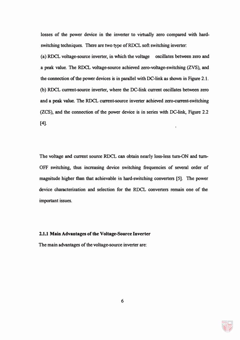
switching techniques. There are two type ofRDCL soft switching inverter:
(a) RDCL voltage-source inverter, in which the voltage oscillates between zero and
a peak value. The RDCL voltage-source achieved zero-voltage-switching (ZVS), and
the connection of the power devices is in parallel with DC-link as shown in Figure 2.1.
(b) RDCL current-source inverter, where the DC-link current oscillates between zero
and a peak value. The RDCL current-source inverter achieved zero-current-switching
(ZCS), and the connection of the power device is in series with DC-link, Figure 2.2
[4].
The voltage and current source RDCL can obtain nearly loss-less turn-ON and turn
OFF switching, thus increasing device switching frequencies of several order of
magnitude higher than that achievable in hard-switching converters [5]. The power
device characterization and selection for the RDCL converters remain one of the
important issues.
2.1.1 Main Advantages of the Voltage-Source Inverter
The main advantages of the voltage-source inverter are:
6

01 03 05
04 06 02
l1
C1 -'-
l
c
Pa :
Figure 2. 1: Voltage-source resonant DC-link inverter.
01 03
04 06 02
Figure 2.1 : Current-source resonant DC-link inverter.
7

(a) The zes has considerably higher losses than the ZVS converter, because
the device in zes circuit is required to carry the full load current while the
device in ZVS circuit converter only need carry the resonant current [6].
(b) Safe operation with an open output circuit.
(c) Suitable for operation above the resonant frequency [7].
2.1.2 RDCL Voltage--Source Inverter
The basic topology for RDCL with zero-voltage-switchin& is that the resonant circuit .
is connected between the DC input voltage and the PWM inverter so that the input
voltage to the inverter oscillates between zero and slightly more than twice the DC
input voltage as presented in Figure 2.3a [8-9]. Assuming that 10 is the current drawn
by the inverter, and that the circuit is loss-less (R = 0), the link voltage, Vc, is:
The inductor current, IL, is
It = VII JC/ L sinCl>ot+ 10
(2. 1)
(2.2)
Under loss-less conditions the oscillation will continue and due to the power loss in R
and It, there is damped sinusoidal and SI is turned ON to bring the current to initial
level. The value of R is small and the circuit is underdamped. Under this condition, It
and V c can be shown as:
8