university of california santa barbara area-efficient
TRANSCRIPT

UNIVERSITY OF CALIFORNIA
Santa Barbara
Area-efficient Neuromorphic Silicon Circuits and Architectures using Spatial and Spatio-
Temporal Approaches
A dissertation submitted in partial satisfaction of the
requirements for the degree Doctor of Philosophy
in Electrical and Computer Engineering
by
Melika Payvand
Committee in charge:
Professor Luke Theogarajan, Chair
Professor Forrest Brewer
Professor Dmitri Strukov
Professor K.-T. Tim Cheng
Professor Wei Lu
December 2016

The dissertation of Melika Payvand is approved.
_____________________________________________
Forrest Brewer
_____________________________________________
Dmitri Strukov
_____________________________________________
K. -T. Tim Cheng
_____________________________________________
Wei Lu
_____________________________________________
Luke Theogarajan, Committee Chair
December 2016

iii
Area-efficient Neuromorphic Silicon Circuits and Architectures using Spatial and Spatio-
Temporal Approaches
Copyright © 2016
by
Melika Payvand

iv
ACKNOWLEDGEMENTS
The past 6 years in UCSB has truly been a life journey in many different aspects. It was a
process of scientific, philosophical, intellectual, psychological and social growth for me. When
I think back I cannot believe how far I’ve come as a person and I owe this to the fantastic
people I’ve met here, in Santa Barbara. I want to dedicate my thesis to them as they formed
these unforgettable years for me.
My advisor, professor Luke Theogarajan, who was always a source of inspiration and a
true mentor, in science and in life. He truly cared about the well-being of all of his students
and I’m honored to have been one of them.
Professor Forrest Brewer who always encouraged curiosity and his breadth of knowledge
was inspirational. He always made me feel that there is so much to learn.
Professor Dmitri Strukov, Professor Tim Cheng and Professor Wei Lu who provided other
perspectives in MURI project and they were always happy to help and listen to me.
Bruno Silva, whose perspective in life changed me to my core. His peace calmed me down,
made me believe that any achievement in life requires patience and good things happen to
people who wait. He brought a sense of meaning and gratitude to my life which nobody has
ever had.
Advait Madhavan, who always offered a hand when I was falling. Who believed in me
when I didn’t and who listened to me when no-one else did. Can’t thank him enough. Doing
tape-out with him is my favorite part of grad school
Amirali Ghofrani, who was family. His support, warmth and positivity always fueled me.
He never failed to bring happiness.

v
Doing a tape out with Amirali, Advait and Miguel Lastras was an incredible experience.
We worked together as a team and learned so much from each other. I very much appreciate
Miguel’s drive in that project for if it wasn’t for his belief in memristors, that chip would have
never got to where it did.
Danielle Morton, who patiently taught me all she thought I should know when I joined the
group and was always happy to help. Her perseverance was always a source of admiration for
me.
Anahita Mirtabatabayi for when she is around everything is better. She shaped the structure
of my life in Santa Barbara and was always a role model for me as a strong woman.
Tanya Das and Oana Catu who never failed to bring joy to my life. They were there when
I needed them the most and gave me so much love.
All of my current and past colleagues in Biomimmetic Circuits and Nano Systems group
for providing such a friendly environment to discuss circuits, science and life and to share
laughter and joy. I appreciate each and every one of them.
Colleen and Alf, who were my family. Can’t thank them enough. They care for me as their
daughter and never failed to give their support.
And, to my family. For they gave me all they had not for the past 6 years but since I started
existing.
My parents who ignited the flames of desire for achievement and success in me.
My sister whose unconditional love warms my heart.
My grandma who is happy with my happiness and sad with my sadness.
My aunt and uncle who embraced me with all they had when I moved to the US.

vi
THANK YOU all for being part of my life and forming my great years of graduate school. I
couldn’t have asked for more.

vii
“The science of the mind can only have for its proper goal the understanding of human
nature by every human being, and through its use, brings peace to every human soul.”
―Alfred Adler

viii
VITA OF MELIKA PAYVAND
December 2016
EDUCATION
PhD, University of California Santa Barbara, Electrical and Computer Engineering Advisor:
Prof. Luke Theogarajan, December 2016
M.S. University of California Santa Barbara, Electrical and Computer Engineering,
Septermber 2012
B.S. University of Tehran, Iran. Electrical and Computer Engineering, July 2010
SUMMARY OF SKILLS
o IC Design, Layout and Test: Full design flow of chip design from transistor level to
layout to post-layout simulations and testing: Neuromorphic VLSI, Analog/ Digital/ Mixed
Signal Circuit Design, FPGA Design, PCB Design
o Machine Learning: Logistic/Softmax Regression, Supervised/Unsupervised Learning,
Convolutional Neural Networks, Auto-encoders, PCA, Sparse Coding, etc.
o Computational Neuroscience: Spike Encoding/Decoding, Information Theory
o Resistive Switching and Memristive Device and Application
RESEARCH AND WORK EXPERIENCE
o Developed A Novel Spatio-Temporal Coding Algorithms for Neuromorphic Chip
Applications: This algorithm uses a combinatorial scheme in spiking patterns of neurons
which learn to recognize patterns in a completely unsupervised fashion. This results in

ix
significantly reducing the number of connections required to do similar tasks using other
counterpart algorithms, Summer 2015-Present
o Tape-out: Configurable CMOS Spiking Neurons for 3D-Memristive Synapses
Design, layout and tape-out of a neuromorphic chip containing an array of CMOS spiking
neurons. Spike shapes are engineered to enable STDP for memristive crossbars and are fully
configurable. The circuit is designed fully asynchronously to enable online unsupervised
learning. The chip is designed in Silterra 180nm. Winer 2015
o Developed a Mapping from Connectivity Domain Available in CMOL Architecture
to Localized Neural Receptive Fields: Explored the use of large fan-in locally connected
spiking silicon neurons readily available in CMOL architecture to solve edge recognition in
images via unsupervised learning. Spring 2015
o Tape-out: Configurable CMOS Memory Platform for 3D Memristor Integration
Involved in a collaborative CMOL (CMOS-Molecular devices) memory development
project. Design, layout and test of the first CMOS memory controller platform for the
memristive memory array in a hybrid/3D architecture. Testing resulted in full functionality of
the chip which was fabricated in On-Semi 3M2P 0.5um occupying 2X2mm2. Summer 2014-
Winter 2014
o Tape-out: Floating Gate Transistor and Photodiode Characterization

x
Design, layout and tape-out of a chip to characterize floating gate transistor current as a result
of hot electron injection into the floating gate. A current sensing scheme using a WTA circuit
was utilized to detect the change in current. Photo-diode current sensing circuit was designed
using a current to frequency conversion for a digital read out. Winter-Spring 2013
PUBLICATIONS
M. Payvand, L. Theogarjan “Winners-Share- All: Towards Exploiting the Information
Capacity in Temporal Codes”, In Manuscript 2016
M. Payvand, L. Theogarajan, “Exploiting Local Connectivity of CMOL Architecture for
Highly Parallel Orientation Selective Neuromorphic Chips”, IEEE/ACM International
Symposium on Nanoscale Architectures (NANOARCH), Boston, Massachusetts, USA, July
2015
M. Payvand, A. Madhavan, M. Lastras, A. Ghofrani, J. Rofeh, T. Cheng, D. Strukov, L.
Theogarajan, “A configurable CMOS memory platform for 3D integrated memristors”,
ISCAS 2015
M. Payvand, J. Rofeh, A. Sodhi, L. Theogarajan, “A CMOS-memristive self -learning neural
network for pattern classification applications”, Nanoarch, July 2014, Paris, France
J. Rofeh, A. Sodhi, M. Payvand, M. Lastras, A. Ghofrani, et al, “Vertical integration of
memristors onto foundry CMOS dies using wafer-scale integration”, ECTC 2015, IEEE 65th.
A. Ghofrani, M. Lastras, S. Gabba, M. Payvand, W. Lu, L. Theograjan, T. Cheng, “A low-
power variation-aware adaptive write scheme for access-transistor-free memristive memory”,
JETC, 2015

xi
AWARDS
Awarded University of California Doctoral Student Travel Grant, July 2015
Awarded Graduate Student Researcher Fellowship (GSR), UC Santa Barbara, 2012-Present
Awarded Best Teaching Assistant Award, Spring 2011
Picked Among the 5% Exceptional Students, Department of ECE, University of Tehran,
2008-2010
Ranked 164 among 500,000 participants nationwide in “University Entrance Exam”, Iran,
Summer 2005

xii
ABSTRACT
Area-efficient Neuromorphic Silicon Architectures using Spatial and Spatio-Temporal
Approaches
by
Melika Payvand
In the field of neuromorphic VLSI connectivity is a huge bottleneck in implementing brain-
inspired circuits due to the large number of synapses needed for performing brain-like
functions. (E.g. pattern recognition, classification, etc.). In this thesis I have addressed this
problem using a two pronged approach namely spatial and temporal.
Spatial: The real-estate occupied by silicon synapses have been an impediment to
implementing neuromorphic circuits. In recent years, memristors have emerged as a nano-scale
analog synapse. Furthermore, these nano-devices can be integrated on top of CMOS chips
enabling the realization of dense neural networks. As a first step in realizing this vision, a
programmable CMOS chip enabling direct integration of memristors was realized. In a
collaborative MURI project, a CMOS memory platform was designed for the memristive
memory array in a hybrid/3D architecture (CMOL architecture) and memristors were
successfully integrated on top of it. After demonstrating feasibility of post-CMOS integration
of memristors, a second design containing an array of spiking CMOS neurons was designed in
a 5mm x 5mm chip in a 180nm CMOS process to explore the role of memristors as synapses
in neuromorphic chips.

xiii
Temporal: While physical miniaturization by integrating memristors is one facet of
realizing area-efficient neural networks, on-chip routing between silicon neurons prevents the
complete realization of complex networks containing large number of neurons. A promising
solution for the connectivity problem is to employ spatio-temporal coding to encode neuronal
information in the time of arrival of the spikes. Temporal codes open up a whole new range of
coding schemes which not only are energy efficient (computation with one spike) but also have
much larger information capacity than their conventional counterparts. This can result in
reducing the number of connections to do similar tasks with traditional rate-based methods.
By choosing an efficient temporal coding scheme we developed a system architecture by
which pattern classification can be done using a “Winners-share-all” instead of a “Winner-
takes-all” mechanism. Winner-takes-all limits the code space to the number of output neurons,
meaning n output neurons can only classify n pattern. In winners-share-all we exploit the code
space provided by the temporal code by training different combination of k out of n neurons
to fire together in response to different patterns. Optimal values of k in order to maximize
information capacity using n output neurons were theoretically determined and utilized. An
unsupervised network of 3 layers was trained to classify 14 patterns of 15 x 15 pixels while
using only 6 output neurons to demonstrate the power of the technique. The reduction in the
number of output neurons results in the reduction of number of training parameters and results
in lower power, area and memory required for the same functionality.

xiv
Table of Contents I. Chapter 1: Introduction ................................................................................... 1
1.1 Silicon Neurons ............................................................................................................................ 3
1.2 Silicon synapses ........................................................................................................................... 4
1.2.1 Capacitors .............................................................................................................................. 4
1.2.2 Flash ...................................................................................................................................... 6
1.2.3 Multiple SRAMs ................................................................................................................... 7
1.3 Overview ...................................................................................................................................... 8
1.3.1 Spatial approach: Memristors ................................................................................................ 8
1.3.2 Spatio-temporal Coding Approach ........................................................................................ 9
II. Chapter 2: Memristors and Memristive Architectures ................................. 10
2.1 What is a memristor? .................................................................................................................. 11
2.2 Memristors as Memory Elements ............................................................................................... 14
2.2.1 Crossbar ................................................................................................................................... 16
2.2.2 CMOL Architecture ............................................................................................................. 18
III. Chapter 3: Memory Access controller for Memristor Applications (MAMA)
Chip ..................................................................................................................... 22
3.1 Chip Architecture ....................................................................................................................... 22
3.2 Writing Circuitry (CMOS Cell Design) ..................................................................................... 23
3.3 Sensing Circuitry ........................................................................................................................ 25
3.4 Measurement Results.................................................................................................................. 27
3.4.1 Writing Circuitry Characterization ...................................................................................... 29
3.4.2 Sensing Circuitry Characterization ...................................................................................... 30
3.4.3 Memristor Characterization Results .................................................................................... 31
IV. Chapter 4: Spiking CMOS Neurons Chip .................................................... 32
4.1 Network Architecture ................................................................................................................. 32
4.2 Spike Timing Dependent Plasticity (STDP) ............................................................................... 34
4.3 CMOS Spiking Neurons (CSN) Chip ......................................................................................... 36
4.3.1 Neuron’s Design .................................................................................................................. 38
4.3.2 Inhibition Network .............................................................................................................. 47
4.3.3 Neural Array ........................................................................................................................ 48
V. Chapter 5: Spatio-temporal Encoding Approach ......................................... 50
5.1 Introduction ................................................................................................................................ 50
xv
5.2 Temporal Codes ......................................................................................................................... 52
5.3 Time as Basis for Information Encoding .................................................................................... 54
5.4 Rank Order Code ........................................................................................................................ 56
5.5 Winners-Share-All (WSA) ......................................................................................................... 59
VI. Chapter 6: Applying WSA to a Classification Problem ............................... 63
6.1 Network Architecture ................................................................................................................. 64
6.1.1 Neuron’s Model ................................................................................................................... 66
6.1.2 Synapse Model .................................................................................................................... 67
6.2 Layer 1: Converting Pixel Intensity into Spikes ......................................................................... 68
6.3 Layer 2: Extracting features from the Images ............................................................................ 69
6.4 Layer 3: Classification ................................................................................................................ 71
6.4.1 Challenge 1: Learning ......................................................................................................... 71
6.4.2 Challenge 2: Inhibition ........................................................................................................ 74
6.4.3 Challenge 3: Correlation in the input patterns ..................................................................... 75
6.4.4 Challenge 4: Greedy Attractor ............................................................................................. 77
6.5 Results .................................................................................................................................. 83
6.5.1 Weight Evolution................................................................................................................. 83
6.5.2 Output Neurons Output ....................................................................................................... 84
6.5.3 Classification ....................................................................................................................... 85
VII. Conclusion and Future Work ................................................................. 88
7.1 Conclusion .................................................................................................................................. 88
7.2 Future Directions ........................................................................................................................ 89
References ........................................................................................................... 91
Appendix I: MATLAB Code developed for Layer 1: Image Intensity to Spike
Conversion .......................................................................................................... 96
Appendix II: MATLAB Code developed for Layer 2: Extracting Features ...... 98
Appendix III: MATLAB Code Developed for Layer 3: Classification ........... 101
List of Figures

xvi
Figure I-1 Axon Hillock Neuron Model [34]. .....................................................................3
Figure I-2 The bistability circuit will drive the w node towards one of its two stable
states.Figure adopted from [3]. ..................................................................................................5
Figure I-3 P-type Synapse Transistor [35]. ..........................................................................6
Figure II-1Memristor realization and typical hysteretic I-V behavior. (a) OFF state: An
initial fil- ament is formed during a one-time formation process. No conductive channel
exists; thus the device is in high resistance state. (b) Set process: positive voltage drifts the
dopants toward the filament, forming a channel, and decreasing the resistance. (c) ON state: a
low-resistance channel is formed between the two electrodes. (d) Reset process: Applying a
negative voltage repels the dopants and ruptures the channel, increasing the resistance.
Adopted from [10]. ..................................................................................................................12
Figure II-2 Memristors' main operating regions; Green: Diode region where tiny current
passes through the device under the application of electric field. Yellow: Red region where
enough current passes through the memristors to sense the state of the device without
changing its state. Red: Switching region where the memristor switches from one state to
another......................................................................................................................................13
Figure II-3 Standard memory architecture. ........................................................................14
Figure II-4 1T-1R architecture. Memristors are accessed through selecting the series
transistor. ..................................................................................................................................15
Figure II-5 Crossbar memristor array with selected bits for reading and writing [11]. .....16
Figure II-6 CMOS Level Chip Architecture [11]. .............................................................17
Figure II-7 Cutting large crossbars into many small ones. Decoding the crossbar is
equivalent to decoding a “blue pin” and decoding a memristor within that mini crossbar is

xvii
equivalent to decoding a “red pin”. Every combination of red and blue chooses a unique
memristor. ................................................................................................................................18
Figure II-8 CMOL architecture consists of reds and blue pins in an area distributed
interface....................................................................................................................................19
Figure II-9 Every red and blue pins are embraced inside a CMOS Cell. Every CMOS Cell
is connected to a neighborhood of CMOS Cells thorough a mini-crossbar. This is shown in
pink in this figure and is dubbed the connectivity domain of the CMOS Cell shown in
gray. .........................................................................................................................................20
Figure III-1 a) Overall chip architecture. b) CMOS cell. When the transmission gates are
selected by Red/Blue enable signals, they connect the Red/Blue lines to the Red/Blue pins
which are the interface to the integrated memristors. c,d) Blue and Red line drivers which
places the appropriate voltages on the Red/Blue lines [15]. ....................................................23
Figure III-2 CMOS cell layout. Metal 3 is used as the interface with integrated
memristors. This cell occupies an area of 32×32 µm2 in a 0.5µm process. ............................24
Figure III-3 Sensing circuitry. a) The current-sensing scheme. The memristor’s current
from the crossbar is compared against a reference current by the winner-take-all (WTA)
circuit. b) A tunable reference current. The current can be changed by tuning the Roff-
chip. ..........................................................................................................................................25
Figure III-4 a) Chip micrograph. Different parts of the chip are shown. b) Individual
devices integrated on the chip. .................................................................................................27
Figure III-5 PCB board designed to test the MAMA chip. ................................................28
Figure III-6 a) Write circuitry characterization. As the resistive load decreases, the
writing voltage drop across the load also decreases. b) Read circuitry characterization. The

xviii
reference current to the WTA is tuned by two orders of magnitude and the response of the
read circuitry is plotted. The highlighted region shows the forbidden zone. c)A checkerboard
pattern is used to program an array of 8x8 devices. The devices with the X,s are either
shorted or failed to get programmed. .......................................................................................29
Figure III-7 3D-integrated memristors on top of MAMA chip. on the left,
Pt/Al2O3/TiO2/Ti/Pt memristors are used from Prof. Strukov's group. On the right, there are
Pd/WOx/W memristors fabricated by Prof. Lu’s group. ..........................................................31
Figure IV-1 Neural Network Architecture. Red circles represent the input neurons while
the blue represent the output neurons. Neurons are modeled with a simple leaky integrate and
fire model. ................................................................................................................................32
Figure IV-2 Applying competition between neurons by lateral inhibition. .......................33
Figure IV-3 Spike Timing Dependent Plasticity as the learning mechanism observed in
the brain. ..................................................................................................................................34
Figure IV-4 Membrane voltage waveforms. Pre-and post-synaptic membrane voltages for
the situations of positive ΔT (A) and negative ΔT (B). Figure is taken from [18]. .................35
Figure IV-5 Generating STDP window by engineering the pulse shape across the
memristors in the crossbar. a) memristor corssbar array. b) pulse shapes engineered to
enforce STDP across the desired memristor. c) Voltage drop across the memristor as a
function of the difference in arrival time of the pre and post synaptic neurons. D) STDP
window generated as a result of the experiment. Figures taken from [19]. .............................36
Figure IV-6 Characteristics of the memristors used for the Spiking Neuron Chip design.
Figure is adopted from [20]. ....................................................................................................37
Figure IV-7 Complete neuron's model with feedforward and feedback pulse shapers. ....38

xix
Figure IV-8 Leaky integrate and fire neuron (1). ..............................................................39
Figure IV-9 Leaky integrate and fire neuron (2) ...............................................................40
Figure IV-10 Complete leaky integrate and fire model. ....................................................41
Figure IV-11 OpAmp topology employed for the integrator in the LIF neuron. The
OpAmp has an extended common mode range at the input with a class A-B push pull at the
output to drive the memristive crossbar array..........................................................................42
Figure IV-12 Amplifier stay stable for more than 2 orders of magnitude to support the
current needed to program the memristors in the crossbar array. ............................................43
Figure IV-13 Desired pulse shape with configurable parameters. .....................................44
Figure IV-14 pulse shaper design. Configurability is enabled through the use of DACs
and clks. ...................................................................................................................................45
Figure IV-15 Spectre simulation results illustrating the configurability of the pulse shape
through DAC (left) and clk (right). ..........................................................................................46
Figure IV-16 Complete layout of the LIF neuron with feedforward and feedback pulse
shapers. Red and Blue pins are placed to enable CMOL implementation of memristors for 3D
integration. ...............................................................................................................................47
Figure IV-17 Inhibition block schematic (left). Layout of one of the 5 sections (right). ..48
Figure IV-18 Complete layout of the LIF neurons 5x5 array. Each neuron takes an area of
500 x 500 µm2. .........................................................................................................................48
Figure IV-19 Chip Micrograph in Silterra 180 nm. ...........................................................49
Figure V-1 Simple model of the biological neurons (left). First mathematical model of the
neurons (right). Figure is taken from [26]. ..............................................................................50

xx
Figure V-2 Neural pathway from the retina to the inferotemporal cortex, where visual
objects are recognized. Figure taken from [36]. ......................................................................51
Figure V-3 Intensity to latency conversion. The stronger the input, the faster the neuron
spikes. Figure is taken from [30]. ............................................................................................52
Figure V-4 Illustration of using temporal codes for computation. Time is divided into
time windows and information can be encoded depending on which neurons spike in each
time window. Figure is taken from [26]. .................................................................................53
Figure V-5 Possible neural codes provided by the temporal coding. Figure is taken from
[37]. ..........................................................................................................................................54
Figure V-6 Competitive Learning- Each output neuron represents a cluster. N_A and
N_B represent cluster A and B respectively and WA and WB are the centers of the clusters.
Upon the arrival of every input pattern, the winner neuron’s weights adjust themselves to get
closer to the input pattern. ........................................................................................................57
Figure V-7 Emergence of selective responses of each neuron to a specific pattern. Lateral
inhibition is applied as a winner takes all mechanism and competitive learning results in the
assignment of each pattern to the emission of one spike from one neuron. Figure is taken
from [30]. .................................................................................................................................59
Figure V-8 Comparison of the number of output neurons required to recognize patterns
between WTA (blue) and WSA (red) mechanism. As the number of patterns increase, the
efficiency of using WSA becomes more apparent. ..................................................................60
Figure V-9 The case with two similar rank codes in which only the rank of two last
spikes are different. ..................................................................................................................61
Figure VI-1 Training set and Test set patterns used for the classification problem. .........63

xxi
Figure VI-2 Neural network architecture used in this work. Intensity is converted to time
of spike in the first layer and features of the image are extracted in the second layer. The
patterns are recognized at the last layer. ..................................................................................65
Figure VI-3 Pulse Width Modulation (PWM) of the pre synaptic input spike in order to
weight the earlier spike more than the later ones. The neuron integrates the dotted green area
under the PWM signals and hence the earlier signals stimulate the neurons more
effectively. ...............................................................................................................................67
Figure VI-4 First layer: converting pixel intensity to spikes. Normalized patterns are
presented to the network every 10 ms and in that time window network processes these
patterns. a) Each neuron is assigned to one pixel. b) Raster plot showing the spiking of 225
neurons in the simulation time. c) zoomed version of the raster plot showing the spiking of
neurons in each 10ms time window in which the patterns are presented. ...............................69
Figure VI-5 Second layer: extracting edges from each kernel. 3x3 kernels are taken from
the image and are convolved with features that are hardwired in the network. This layer of
neurons responds to dominant edges existing in each 3x3 kernel. ..........................................70
Figure VI-7 Spiking learning algorithm developed for WSA. Calcium concentration
models are used as part of the Anti-STDP rule to calculate dwp and dwn. .............................73
Figure VI-8 Inhibitory neuron designed to ensure not more than half of the output
neurons fire at any given time window. ...................................................................................75
Figure VI-9 Habituation neuron designed to ignore the similarities between the input
patterns and look for the differences between patterns which helps to separate patterns........76

xxii
Figure VI-10 Concept of homeostatic plasticity in the brain. Feedback mechanisms are
applied in order to keep the firing rate of a neuron in a target range. Figures are taken from
[32]. ..........................................................................................................................................78
Figure VI-11 Neural State Machine (NSM) designed to control the appearance frequency
of the WSA codes. ...................................................................................................................80
Figure VI-12 Weight evolution showing the weights converging to analog values. .........83
Figure VI-13 Network performance on the test set. On the left, the network accuracy
converges to 87%. On the right, each pattern gets assigned to a unique combination from a
set of 41 codes in the code space. ............................................................................................85
Figure VI-14 Edit distance vs Pattern similarity for all the patterns. ................................86
Figure VII-1 400 features extracted from MNIST training set by training an
autoencoder. .............................................................................................................................89

xxiii

1
I. Chapter 1: Introduction
There has been a long standing dream to make computers that work like the brain and
scientist have been working on this problem for decades now. However, the gap between the
state-of-the-art computers and the brain is still very large. The most important reasons why are
because:
1) Computers and the brain have a fundamentally different way of computing. Computers
have a deterministic approach in processing the input data. There are well-defined logic
gates which take 0 and 1 logic levels as inputs, and output appropriate 0s and 1s depending
on the logic function. Whereas the brain takes a self-organizing method of computation,
meaning that it learns from mistakes. Let me give the example of throwing a ball into the
basket. If we were to program a conventional computer to achieve this, all the physical
laws of gravity would have had to be defined in the program, taking into account details
such as the size of the ball, and also environmental factors such as the wind or rain and ask
the computer to calculate the initial velocity and direction of throwing the ball in order to
make it to the basket. The brain, however, has a completely different approach. The ball is
thrown and if it does not make it to the basket, it learns from its mistake. The solution to
the problem of targeting the ball into the basket overshoots and undershoots until the goal
is reached. That’s how the brain self-organizes the solution to an unknown problem, by
trial and error.
2) In computers the execution of instructions is rather sequential. The reason why I say
“rather” is because today’s computers take advantage of a lot of parallelization using
GPUs. However, the parallelization works as dividing tasks between different processing
cores but execution of each task at a specific core is still sequential. This is while the brain

2
processes information massively in parallel: millions of processing units all working at the
same time.
3) While brain uses these millions of processing units in parallel, which are connected to
each other through billions of connections, it only consumes a few tens of watts. If we were
to run “human-scale” simulations of the brain running in real time, using the best
supercomputers, that would consume about 12 Giga watts of power. [1]
The reasons mentioned above makes it clear why building a “brain-inspired” computer is the
next computing paradigm. These computers will be
a) Efficient in terms of energy and space
b) Scalable to large networks
c) Flexible enough to run complex behavioral model
Considering how far we have come in silicon industry and all the advances in the field of
neuroscience and AI, could make us wonder what is stopping us from making these computers?
The answer lies of course in limitations we face because of the physical properties of silicon
chips. Below I will talk about the major bottlenecks of building such computers.
Bottlenecks of implementing brain-inspired computers
Centralized von Neumann architecture is fundamentally not suitable for representing
massively interconnected neural networks. In this type of architecture, used in conventional
computers, the processing unit and the memory are separated from each other. When there is
an instruction to be executed, special part of the memory is addressed, the data is fetched and
is processed in the CPU. This is fundamentally in contradiction with how the brain performs
the computation where the memory is localized to the processing unit and is distributed all

3
across the brain. In order to make brain-like computers we should also use these distributed
computing-memory agents, namely neurons and synapses.
1.1 Silicon Neurons
Silicon neurons emulate the electro-physiological behavior of real neurons. This may be
done at many different levels, from simple models (like leaky integrate-and-fire neurons) to
models emulating multiple ion channels and detailed morphology. Depending on the
application and the level of sophistication required, different models could be used. Leaky
integrate and fire models are less realistic and do not take into account many of the details of
what’s going on inside a neuronal cell. But they are simple and need very small area since the
number of transistors used in the circuit is minimal.
The first leaky integrate and fire model which was proposed by Carver Mead in the late
1980s is shown in Figure I-1. In this circuit, a capacitor that represents the neuron’s membrane
lipid bilayer integrates input current into the neuron. As soon as the capacitor reaches the
neuron’s threshold, a pulse Vout is generated, the membrane potential Vmem is reset through the
NMOS transistors and the neuron will be ready for the next current injection.
Figure I-1 Axon Hillock Neuron Model [34].

4
1.2 Silicon synapses
Conceptually, synapses can be modeled as the connection between neurons with an
associated strength (weight). In fact, synapses are the adaptive learning agents in the brain:
Neurons receive inputs and fire, so they have a very specific task: when the membrane potential
is above a threshold, they fire. However, the synapse’s strength has dynamics and will change
in the process of learning. These changes are continuous and analog rather than digital.
Therefore, in order to mimic the synaptic behavior into the silicon we need nonvolatile analog
memory storage with locally computed memory updates. Note that in order to perform brain-
like functions, a large number of artificial synapses are needed.
Throughout the history of neuromorphic engineering, circuit designers tried many different
options as analog memory for artificial synapses. I’ll briefly go over each of them below.
1.2.1 Capacitors
Capacitors are the first obvious choice for analog memory. They accumulate the charge
and develop a voltage across their capacitive plate. The only important problem is that they
leak. So they are not truly non-volatile as they slowly lose the charge. However, different
solutions have been proposed to overcome this problem. For example, using techniques such
as generating negative gate-source voltage across the series transistor in order to reduce the
leakage below the “off subthreshold current” [2], or using them only as an analog memory
while learning ,and then register the value as a single digital bit depending on the analog value
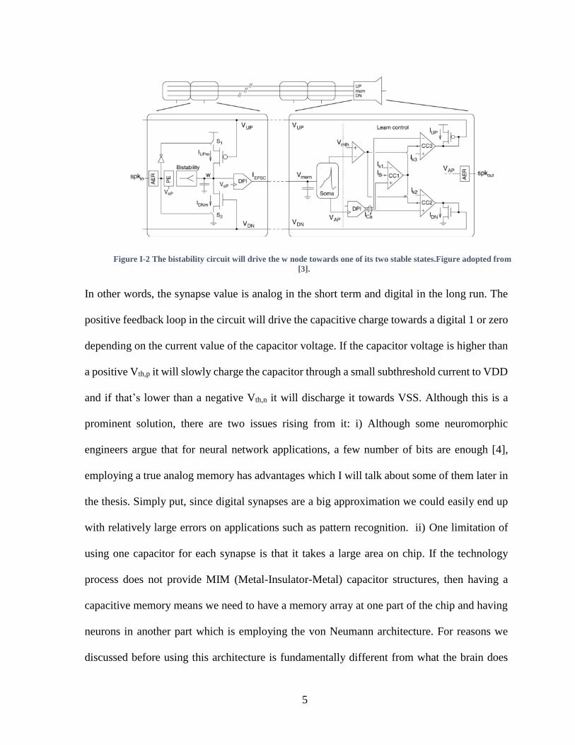
of the capacitor voltage. This is called Fusi learning [3]. The idea is presented in Figure I-2
shown below.
5
In other words, the synapse value is analog in the short term and digital in the long run. The
positive feedback loop in the circuit will drive the capacitive charge towards a digital 1 or zero
depending on the current value of the capacitor voltage. If the capacitor voltage is higher than
a positive Vth,p it will slowly charge the capacitor through a small subthreshold current to VDD
and if that’s lower than a negative Vth,n it will discharge it towards VSS. Although this is a
prominent solution, there are two issues rising from it: i) Although some neuromorphic
engineers argue that for neural network applications, a few number of bits are enough [4],
employing a true analog memory has advantages which I will talk about some of them later in
the thesis. Simply put, since digital synapses are a big approximation we could easily end up
with relatively large errors on applications such as pattern recognition. ii) One limitation of
using one capacitor for each synapse is that it takes a large area on chip. If the technology
process does not provide MIM (Metal-Insulator-Metal) capacitor structures, then having a
capacitive memory means we need to have a memory array at one part of the chip and having
neurons in another part which is employing the von Neumann architecture. For reasons we
discussed before using this architecture is fundamentally different from what the brain does
Figure I-2 The bistability circuit will drive the w node towards one of its two stable states.Figure adopted from
[3].

6
and will limit us in parallelizing the structure. Even if the technology process provides a MIM
capacitor structure, the supporting circuity needed for each synapse in order to enable online-
learning is very area-hungry and will only work for small networks.
1.2.2 Flash
In the late 90s, C. Diorio and his colleagues in Carver Mead’s lab fabricated synapse
transistors that not only possessed nonvolatile analog storage, and compute locally their own
memory updates, but also allowed local computation of the product of their stored memory
value and the applied input. To ensure nonvolatile storage, they used standard floating-gate
MOS technology, but adapted the physical processes that write the memory to perform a local
learning function [5]. Figure I-3 shows the p-type of this synapse transistor.
The underlying process of non-volatility of the memory lies in trapping electrons in the
floating gate by employing hot-electron injection which is a well-known process in MOSFETs.
Figure I-3 P-type Synapse Transistor [35].

7
It occurs in short-channel devices with continuous channel currents, when a high gate voltage
is combined with a large potential drop across the short channel. Injecting electrons into the
floating gate will cause a negative voltage to develop on the gate and hence it will decrease the
threshold voltage of the PMOS, increasing the “weight” of the synapse transistor. On the
contrary, in order to remove charge from the floating gate and decrease the synaptic “weight”,
positive high voltages should be applied to the tunneling implant to remove electrons from the
floating gate, thereby increasing the floating gate voltage.
The advantage of this method is that the weight multiplication by the input is done locally
and without any extra circuity. So it’s area-efficient and local. The disadvantages of using these
synapse transistors are i) There is not a full-blown model of these transistors available in CAD
tools such as Cadence virtuoso. Therefore, when laying out these devices, the standard CMOS
process transistors cannot be used and hence the functionality of these devices cannot be
ensured before their fabrication. ii) Increasing and decreasing the weights are not trivial. High
voltages are needed in order to facilitate hot-electron-injection and tunneling mechanisms.
These high voltages need to be generated on chip (or by connecting from an I/O whose ESD
protection diodes have been removed) and will decrease the oxide life time.
1.2.3 Multiple SRAMs
Yet another method of building electronic synapses employed by researcher throughout the
years have been to use multiple SRAMS [6]. In this method, few bits of memory are devoted
to each synapse. Analog values of synapse are digitized using a DAC and are kept in the
SRAM. When reading, the SRAM memory bits are fed into an ADC and the analog value is
used in the circuit. The advantage of this method is that it’s very robust since the memory is
kept digitally. The disadvantages are i) it’s volatile. So with the loss of power the memory will

8
be reset. ii) It’s very computationally expensive and area inefficient to use an ADC and a DAC
for every synapse. These ADCs and DACs can be shared but that serializes the process and
also needs extra circuitry in order to priority encode which synapse will take use of the shared
DAC and the ADC.
1.3 Overview
As stated above, one of the most important bottlenecks of building computers that work
like the brain, is to make artificial synapses. Although there have been many attempted
solutions for this problem, packing a large number of silicon synapses in a small area enabling
the local learning remains an issue. In this thesis, I have investigated a two pronged approach
namely spatial and temporal to tackle this problem.
1.3.1 Spatial approach: Memristors
In recent years, memristors have emerged as a solution for the connectivity problem. These
nano-devices can be densely integrated on top of CMOS chips and can serve as analog memory
needed to imitate synapses. What makes memristors a perfect candidate as an artificial synapse
is not only because they have a nano-size footprint and they take no silicon space, but also they
are non-volatile analog memory. Also, they imitate biological synapses very well since the
multiplication of the weight (Memristor’s conductance G) to the input current (I) occurs
automatically through Ohm’s law (I=GV). The adaptive conductance of the material could
serve as “analog weights” which develop voltages across the devices, depending on the current
passing through them as inputs to the network.
As a first step in realizing integrated memristors as artificial synapses, we designed a
programmable CMOS chip enabling direct integration of memristor. In a collaborative MURI

9
project, a CMOS memory platform was realized for the memristive memory array in a
hybrid/3D architecture (CMOL architecture [7]) and memristors were successfully integrated
on top of it. After demonstrating feasibility of post-CMOS integration of memristors, we
designed a second chip containing an array of spiking CMOS neurons with an area of 5mm x
5mm in a 180nm CMOS process to explore the role of memristors as synapses in neuromorphic
chips.
1.3.2 Spatio-temporal Coding Approach
While physical miniaturization by integrating memristors is one facet of realizing area-
efficient neural networks, on-chip routing between silicon neurons prevents the complete
realization of complex networks containing large number of neurons. A promising solution for
the connectivity problem is to employ spatio-temporal coding to encode neuronal information
in the time of arrival of the spikes. Temporal codes open up a whole new range of coding
schemes which not only are energy efficient (computation with one spike) but also have much
larger information capacity than their conventional counterparts. This can result in reducing
the number of connections to do similar tasks with traditional rate-based methods.
By choosing an efficient temporal coding scheme, I have developed a system architecture
by which pattern classification can be done using a new algorithm dubbed “Winners-share-all”
instead of a “Winner-takes-all” mechanism. Winner-takes-all limits the code space to the
number of output neurons, meaning n output neurons can only classify n pattern. In winners-
share-all we exploit the code space provided by the temporal code by training different
combination of k out of n neurons to fire together in response to different patterns

10
This thesis will be divided into two major parts: Spatial and Spatio-Temporal approach. In
Chapter 2,3, and 4, I cover the spatial approach which studies the role of memristors as
synapses in neuromorphic chips. In chapter 2, I briefly introduce memristors and talk about
some of the background work on different memristive architectures. Chapter 3 will cover the
details of the first chip we taped out which incorporated a means for 3D-integrating Memristive
Arrays for Memory Applications (MAMA). After demonstrating the feasibility of post-CMOS
integration of memristors on MAMA chip, I then explain, in chapter 4, how we took the next
step to design an array of spiking CMOS neurons on a second chip to explore the role of
memristors as synapses in neuromorphic chips.
The second part of this thesis is devoted to the Spatio-temporal coding approach to
reduce the number of connectivity needed on chip by exploring the code space provided by the
temporal codes. Chapter 5 will introduce the concept of information encoding in time and a
summary of background work on this area. I will then propose the Winners-Share-All (WSA)
algorithm using the temporal code and compare it to the conventional Winner-Takes-All
(WTA) counterpart. In chapter 6, I describe how I used this new algorithm to perform a rather
simple recognition task to cluster 14 letters of English alphabet. And finally chapter 7 will
summarize the work of this PhD thesis and discuss the future directions.
II. Chapter 2: Memristors and Memristive Architectures
As the basic building block of electronics, field effect transistor (FET), approaches the 10-
nanometer regime, a number of fundamental and practical issues start to emerge due to

11
difficulties in nanometer-resolution fabrication, electrostatic control and power management.
New devices and architectures are expected to continue the scaling trend the semiconductor
industry has enjoyed in the past decades. Two-terminal resistive switches (also called
memristive devices or memristors) have attracted increasing interest as a suitable alternative
to complement transistors. [8]. In this chapter I introduce memristors and explain its underlying
mechanism. I will also talk about the architectures developed for these nano-devices and how
they can be used for neuromorphic applications.
2.1 What is a memristor?
As can be guessed by the name, it’s a memory resistor: A two-terminal switch which can
retain its resistive state based on the history of the applied field and hence it’s an analog non-
volatile memory. They are simple passive circuit elements, but their function cannot be
replicated by any combination of fundamental resistors, capacitors and inductors [9].
Memristors are typically based on a Metal-Insulator-Metal (MIM) structure. An otherwise
insulating film is sandwiched between two conductive electrodes. The choice of material for
this MIM structure has been under extensive research with different stacks. The underlying
switching mechanism seems to differ for a variety of electrode and memristive materials:
The mechanism can be attributed to a) phase change due to Joule heating in chalcogenide-
based phase-change memories. b) conductive filament formation due to Joule heating observed
in certain oxides such as TiO2. c) conductive filament formation due to electrochemical redox

12
processes observed in binary oxides (e.g. NiO, CuO2, TiO2) or chalcogenides, and polymers d)
field-assisted drift/diffusion of ions in amorphous films and e) possible conformational
changes in molecules. [8]
Figure II-1 shows an example of a memristors in which Pt is used as the electrode and TiO2
as the switching material. There are also some oxygen vacancies in the form of TiO2-x which
act as charged dopants and can respond to the electric field. In the initial state, a filament of
conductive TiO2-x is formed in the non-conductive TiO2 film in an irreversible forming step.
However, the formed filament does not connect the two electrodes together and thus the device
is in a High Resistance State (HRS). In order to switch the device ON, a sufficiently high
positive voltage is applied across the device which attracts positively charged vacancies in the
Figure II-1Memristor realization and typical hysteretic I-V behavior. (a) OFF state: An initial fil- ament is
formed during a one-time formation process. No conductive channel exists; thus the device is in high resistance state.
(b) Set process: positive voltage drifts the dopants toward the filament, forming a channel, and decreasing the
resistance. (c) ON state: a low-resistance channel is formed between the two electrodes. (d) Reset process: Applying
a negative voltage repels the dopants and ruptures the channel, increasing the resistance. Adopted from [10].

13
oxide to the top electrode. This will cause the filament to grow since the vacancies start to drift
through the most favorable diffusion paths in the presence of the electric field and hence they
form a channel between the two electrodes. Once such highly conductive channels are formed,
the device is in Low Resistance State (LRS) and considered as ON [10].
The onset of the figure is illustrating the I-V characteristics of the memristors which
exhibits an inherent memory with a “pinched hysteresis” which can be used for information
storage. For example, in the case of resistive memory RRAM, by assigning LRS=”1” and
HRS=”0”, or in the case of analog memristors, a spectrum of resistive values ranging from a
HRS to a LRS.
The I-V characteristic of memristors have 3 main operating regions which are highlighted
in Figure II-2. The green region in the middle is called a “diode region” where the device acts
like a reverse biased diode. In the diode region, there is very little current passing by for the
voltage being applied across the device. The region shown in yellow is the “read region” in
which the state of the device can be read without changing or disturbing its value, since the
Figure II-2 Memristors' main operating regions; Green: Diode region where tiny current passes through the
device under the application of electric field. Yellow: Red region where enough current passes through the
memristors to sense the state of the device without changing its state. Red: Switching region where the memristor
switches from one state to another.
V
I
0
state OFF
state ON
state ON

14
voltage is not high enough to surpass the device threshold for switching. The voltage range in
the yellow region is “read voltage” which is applied across the device and by sensing the
current passing through, the resistance of the memristor can be measured. The region illustrated
in Red in Figure II-2 is where the device switches to the other state. This “write region” consists
of voltage levels which are greater than the threshold voltage of the device and hence are strong
enough to move the dopants and change its resistance.
These three main operating regions provide a design tool in order to use these devices as
memory elements and perform the desired operation on them.
2.2 Memristors as Memory Elements
As a first step in using memristors as memory elements we can think of replacing them
with conventional memory elements in standard memory platforms. Figure II-3 shows such
platform in which each memory device has an access transistor in series and a certain address
Figure II-3 Standard memory architecture.
Ro
w D
ecod
er
Col Dec
n
n-k k
Address

15
in the array accessible by its row and the column. The address is fed serially to the array, the
row and the column are decoded and the desired operation (read/write) is performed.
Replacing these memory devices with memristors, we end up with an architecture dubbed
“1T-1R”, shown in Figure II-4, which consists of one resistive memory in series with one
access transistor at each row and column.
However, having a series transistor defeats the purpose of using these nano-devices for
high-density packing of the memory since for each memory element, the limitation is still the
size of the transistor. Moreover, the current needed for switching of these devices, depending
on the range of the memristor can range anywhere from 10s of µAs to 10s of mAs which
applies a constraint on the size required for the series transistor having to be able to drive the
required current for switching of its corresponding memristor. So can we somehow remove the
access transistor? The problem raised by doing so is addressability of the memory elements.
The reason why the transistor is addressable is because it’s a 3 terminal device; However, by
removing the access transistor we are now left with a completely resistive array which is called
Figure II-4 1T-1R architecture. Memristors are accessed through selecting the series transistor.
Decoder
DCD1DCD0
DCD
A1
An
MUX
+ _Vth

16
the “crossbar array”. The crossbar array can be implemented using 2 perpendicular layers of
parallel nanowires where a memristor is formed at each cross section. In the following section
I will explain how crossbar arrays can be used to replace conventional memory for a highly
dense memory array.
2.2.1 Crossbar
As was discussed in the previous section, in order to gain from the density of memristors,
cross bar arrays are used, however, their use comes with challenges since the array is fully
passive which I will be addressing in this section.
Selecting the devices in the crossbar array is performed through the application of appropriate
voltages across the horizontal and vertical nanowire of the desired memristor. Figure II-5
illustrates this idea for the read and the write mode.
One row can be read simultaneously by applying Vr, a voltage in the read region of the
memristor, on the horizontal line and pinning the other side, the vertical line, to zero and
reading off the current using a trans-impedance amplifier. To program an individual memristor
to a HRS (“0”) or to a LRS (“1”) -Vw or Vw should be applied across the memristor
Figure II-5 Crossbar memristor array with selected bits for reading and writing [11].
Read
Write 1

17
respectively. However, having Vw on one side and 0 on the other side, will cause unwanted
memory elements to get programmed which is undesirable. In order to solve that problem, to
program a certain memristor, Vw/2 is applied to one side and -Vw/2 is applied to the other side.
This way, the non-selected devices have half of the Vw across them which is designed to lie in
the read region and therefore it does not cause a state change in the device [11].
Figure II-6 depicts the CMOS level chip architecture to support the crossbar array. 3
level muxes at row and column are used to determine the read/write mode, the row/column
select and Write 0 or Write 1 for the write mode. By choosing these 3 bits, desired operation
is done on the desired memristors.
Overall, the memristor-based crossbar network structure can offer the following advantages:
1) it allows ultra-high density memory storage with relatively small number of control
electrodes: n2 cross-points can be accessed by n-rows and n-columns in the crossbar; 2) it
offers large connectivity between devices; and each column or row is connected to n-rows or
columns through n different devices. However, a new challenge rises as the size of the
Figure II-6 CMOS Level Chip Architecture [11].
RowSelect
R/WSelect
Set/Reset
Write Mode
Read Mode
Read Mode
R/WSelect
ColumnSelect
Write Mode

18
crossbars gets larger and larger since the parasitic resistance of the nano-wire becomes
comparable to the memristance and the applied voltages to the crossbars will drop across the
parasitic resistance instead of the memory device. Moreover, the speed of the write or read
deteriorates a lot because of the large capacitances on the nanowire caused by the large size of
the crossbar. In the next section of this chapter I introduce CMOL architecture which tackles
this problem to enable high density 3D memory in CMOS chips.
2.2.2 CMOL Architecture
CMOL architecture was first introduced by Strukov. et al in [12] as a solution for densely
packing memristive devices on top of CMOS chips and I’ll be explaining it from my own point
of view in this section.
As I mentioned before, the problem with large crossbars becomes the undesired parasitic on
the nano-wires. Therefore, instead of having a large crossbar we could instead use multiple
smaller crossbars. This idea is shown in Figure II-7. In order to address an individual device,
one row and column is required to address the crossbar in which the device is located in, and
one row and column is required to address the device within the crossbar. Therefore, a double
Figure II-7 Cutting large crossbars into many small ones. Decoding the crossbar is equivalent to decoding a “blue
pin” and decoding a memristor within that mini crossbar is equivalent to decoding a “red pin”. Every combination of
red and blue chooses a unique memristor.

19
decoding scheme is asked for in order to access the device. In CMOL terminology, we call
addressing the crossbar, selecting the “blue pin” and selecting the device inside the crossbar,
decoding the “red pin”.
If these red and blue pins are distributed in the CMOS surface, we end up with an area
distributed interface as is shown in Figure II-8 .Addressing each blue pin will select an area of
crossbars and addressing the red pin within that region selects the desired device. Each square
containing one blue and one red pin is a “CMOS Cell” which contains the supporting CMOS
circuitry for addressing the memristive devices. The red and the blue pin are the interface
connecting the underlying CMOS to the integrated top and bottom crossbar nanowires,
respectively.
This seems to be solving all the problems, however, if the crossbars are fabricated in a
Manhattan grid fashion, the pitch between the crossbars are dictated by the CMOS cells pitch
which is much larger than the memristive nano-size and it defeats the purpose of employing
memristors. Therefore, in order to exploit the intrinsic nanoscale dimensions of memristors,
decoupling the underlying CMOS feature size from the device is required. One method of
Figure II-8 CMOL architecture consists of reds and blue pins in an area distributed interface.

20
decoupling is to rotate the nanowires. Such rotation ensures that a shift by one nanowire
corresponds to the shift from one interface pin to the next one (in the next row of similar pins),
while a shift by r nanowires leads to the next pin in the same rows (Figure II-9). The bottom
nanowires are passed through blue pins and the perpendicular top nanowires are passed through
red pins. At the cross-point of these nanowires memristors are formed which are addressable
through the red and the blue pin connecting to its corresponding nanowires. This is
demonstrated in Figure 2.9. The colored region highlights the crossbar selected by addressing
the blue pin shown with a larger blue circle. The CMOS cell containing this blue pin is
connected to all the CMOS cells in the highlighted region through the memristive cross points
inside this region. Therefore, the colored area is the “connectivity domain” of the selected
CMOS cell. The device marked by X inside the colored region can be selected by addressing
its corresponding red pin illustrated with the large red circle in Figure II-9.
CMOL tackles fabrication issues such as interlayer alignment accuracy and integration of
nanoscale devices over a CMOS sub-system with larger scale feature size. Moreover, it
Figure II-9 Every red and blue pins are embraced inside a CMOS Cell. Every CMOS Cell is connected to a
neighborhood of CMOS Cells thorough a mini-crossbar. This is shown in pink in this figure and is dubbed the
connectivity domain of the CMOS Cell shown in gray.
CMOS Cell

21
provides high- density memory with less parasitics by sharing select circuitry between multiple
memristors (1T-1R vs 1T-NR).
How can we use this architecture in order to design functional memory arrays? This is the
question I will be answering in the next chapter by describing the CMOS memory platform we
designed in CMOL architecture for 3D memristor integration.

22
III. Chapter 3: Memory Access controller for Memristor
Applications (MAMA) Chip
With this vision of a monolithic, 3D-integrated CMOL memory platform in mind, we have
designed and tested the first prototype of the CMOL architecture complete with integrated
memristors. This chapter focuses on the challenges involved from a circuit design perspective
and the steps taken to support memristors with different ranges of resistance, threshold
voltages, on/off ratio etc. More in-depth analysis of the architectural trade-offs can be found
in [13] and details of the memristor integration is discussed in [14].
The plethora of memristive device designs, each with their unique advantages, requires a
flexible supporting circuit architecture. The circuit design is strongly influenced by the
connectivity imposed by the area-distributed interface and also the chip architecture which is
designed to reflect the CMOL idea. We term this versatile chip the Memory Access controller
for Memristor Applications (MAMA). A key circuit requirement for the MAMA chip is the
ability to handle memristors with different Ron/Roff values, and provide the appropriate write
and read voltages. This chapter explains the configurable architecture and circuits designed as
a platform for integrating different kinds of memristors.
3.1 Chip Architecture
The chip consists of an array of CMOS cells, double decoders, programming drivers and
sensing circuitry shown in blocks in Figure III-1 a. Each CMOS cell houses select circuitry
including Red and Blue pins required by the area-distributed interface (Figure III-1 b).

23
Selecting two of these Red and Blue pins accesses two of the segmented nanowires and hence
a unique memristive device at the cross-point. A row-column decoder in turn accesses these
pins. Thus it requires a double decoding scheme. The double decoders surround the CMOS
cell array and have their function split among the Blue/Red row/column decoders. Depending
on the desired operation (Read/Write) the Blue/Red line drivers place appropriate voltages on
the Red and Blue lines (Figure III-1. c,d) which connects to the Red/Blue pins through the
CMOS Cell select circuitry (Figure III-1 b). For example, during the read operation, Vr is
applied across the desired memory cell and the sensing circuitry makes a binary decision
regarding the memristor state and the data is shifted out serially. In the following sections the
details of the circuitry in these blocks are described.
3.2 Writing Circuitry (CMOS Cell Design)
To write on a particular memristor, the device is addressed and the appropriate write
voltages are applied across it. This is done through CMOS cells shown in Figure III-1 b. It
includes two transmission gates controlled by Blue/Red enable signals routed from the double
decoder. When the gates are asserted, they drive the Red and Blue pins with the appropriate
Figure III-1 a) Overall chip architecture. b) CMOS cell. When the transmission gates are selected by Red/Blue enable
signals, they connect the Red/Blue lines to the Red/Blue pins which are the interface to the integrated memristors. c,d)
Blue and Red line drivers which places the appropriate voltages on the Red/Blue lines [15].

24
voltages on the Blue/Red lines. De-assertion connects the pins to a default voltage, Vd, in order
to avoid floating problems such as leakage or unpredictable state-changes due to unwanted
noise sources.
The transmission gates together with the memristors comprise a voltage divider. To ensure
the memristor’s operation in the desired region (i.e. the write region), the voltage drop across
the transmission gates must be negligible. Therefore, these pass gates need to be sized
accordingly.
However, the size of the transmission gates imposes a limitation on the number of CMOS
Cells which can fit in the chip and hence the size of the memory supported by the chip. As a
result, there is a trade-off between the maximum current drive and the size of the integrated
memory on the chip.
Given these constraints, a size of W/L=42µm/0.6µm in 0.5 µm process is chosen for the
pass gate transistors. The maximum current supported by these transmission gates for a range
of input voltages is reported in the next section. This maximum current can be considered as
the compliance current limiting the current passing through the memristors and hence
Figure III-2 CMOS cell layout. Metal 3 is used as the interface with integrated memristors. This cell occupies an
area of 32×32 µm2 in a 0.5µm process.
Red Enable
GND
Red Enable
VDD
Blue Enable
GND
Blue Enable
M3 : Red Pin
M3 : Blue Pin
Red Line Blue Line

25
preventing device break down [9]. Depending on the required write voltage, the minimum
resistance supported by the chip can be calculated.
Layout realization of a CMOS cell is shown in Figure III-2. Since this CMOS chip needs
to be post-processed for 3D memristor integration, the last metal layer in the On-Semi 0.5µm
process (Metal 3) is crucial to the area-distributed interface. General power and ground routing
cannot be done on this metal layer as it risks exposing and damaging these lines, therefore they
are routed in Metal 2. The size of the pins comprising this area-distributed interface has been
intentionally made large (24×8 µm2) to reduce the effect of cumulative alignment error.
3.3 Sensing Circuitry
In order to make a binary decision regarding the memristor state, a current-sensing scheme
is chosen over a voltage-sensing counterpart. In a conventional voltage-sensing scheme, a
transimpedence amplifier (TIA) is utilized to convert the signal into a voltage which is then
compared against a threshold voltage. However, the TIA needs at least a two stage op-amp
Figure III-3 Sensing circuitry. a) The current-sensing scheme. The memristor’s current from the crossbar is
compared against a reference current by the winner-take-all (WTA) circuit. b) A tunable reference current. The
current can be changed by tuning the Roff-chip.
Vout
WTA
M1
01
M2
01
(b)
(a)

26
with an appropriate output stage in order to drive the resistive load. Moreover, for a high
resistive gain of the TIA, a large feedback resistor is needed, which takes up a large silicon
area. Therefore, for a more compact design, the current-sensing scheme is utilized. Also, a
current-sensing scheme has the advantage of a much larger dynamic range, which is required
for the configurability.
Figure III-3 a shows the schematic of the current-sensing circuitry. The current drawn by
the device in response to a small read voltage, Vr, is compared against a reference current. The
read voltage should be picked in a region where the memristor’s state does not change. This
read voltage is applied by pinning one terminal of the memristor of interest to the default
voltage, Vd, by an op-amp, while the other terminal is driven by the blue line driver to Vd+Vr.
This read current is then compared against a reference current using a winner-take-all (WTA)
circuit.
As the sensing circuitry is only connected to the memristors when the Read En signal is
asserted, the pinning loop is not always closed. In order to avoid the settling time of the loop
when the Read En signal asserts, a very small Ioff current (50 pA, through pbiasdifsr and
pcasdifsr generated from a current diffuser) is passing through M1 while Read En is not active.
As soon as Read En is activated, the Ioff current is steered to an alternate path and is drained
by M2.
In order to make the sensing circuitry compatible with different memristor types (e.g.
different Ron and Roff values), a tunable reference current is designed. As is shown in Figure
III-3 b, this current reference can be tuned by two knobs: the off-chip resistor and the DAC
output voltage across that resistor. A flexible platform for generating the read and write
voltages is designed on the PCB test board by using DAC-controlled voltage sources.

27
3.4 Measurement Results
The chip micrograph is shown in Figure III-4 a. It occupies an area of 2×2 mm2 and was
fabricated in On-Semi 3M2P 0.5µm technology through the MOSIS service. This area can
potentially support 1kb of memory. Using an advanced CMOS technology node will allow for
a larger memory size and smaller CMOS cell size. The range of voltages required for different
Figure III-4 a) Chip micrograph. Different parts of the chip are shown. b) Individual devices integrated on the
chip.
24X36 CMOS CellsB
lue
/Re
d R
ow
De
cod
er
Blue Column Decoder/Line Driver
Red Column Decoder/Line Driver
Read Circuitry
CurrentSource
(a) (b)

28
memristor types coupled with the fabrication cost make 0.5µm technology ideal for this
multipurpose chip.
In order to test the functionality of the chip independent of successful memristor
integration, the last row of the CMOS cell arrays is connected to peripheral bond pads. We
used a potentiometer connected to two of these pads to verify the functionality of the chip over
a large range of resistances, since a memristor is essentially a resistor in steady state. The PC
board designed for testing the chip is shown in Figure III-5. On the right DAC voltages are
configured using an FPGA in order to configure the writing and read voltage of the memristors.
Digital inputs are given through the connectors on both sides of the chip controlled by the
FPGA. The experimental characterization of the chip along with the memristor integration
results are reported in this section.
Figure III-5 PCB board designed to test the MAMA chip.
DACs providing Read and writevoltages. The voltages from top to bottom:
and .This will give us the Flexibility to change The read and write voltages for different kinds of memristors
Connectors to connect devices to the chipexternally to confirm chip’s functionality
4 External TIAsfor even more
flexibility!
Direct connections from the Memristorsin case of using a probe station
DigitalInputs andoutputs

29
3.4.1 Writing Circuitry Characterization
The most important factor of the MAMA chip writing circuitry is the maximum current
drive for the various memristive loads. As is explained in section 3.2, decreasing the load
resistance lowers the voltage drop across the memristor, which limits the current drive. Figure
III-6 a. reports the voltage across a large range of load resistances for different writing voltages.
The highlighted region (below 2kΩ) shows the memristor range not supported by this chip
since the voltage drop across the transmission gates becomes dominant. Table 3.1 depicts the
maximum current provided by the chip in the writing mode for a 10% drop of the writing
voltages.
Table 3.1. Maximum current in the writing mode for a 10% drop of the writing voltage across the gates.
Writing Voltage (V) 1 2 3 4 5
Current (µA) 90 178 183 213 260
Figure III-6 a) Write circuitry characterization. As the resistive load decreases, the writing voltage drop across the load
also decreases. b) Read circuitry characterization. The reference current to the WTA is tuned by two orders of magnitude
and the response of the read circuitry is plotted. The highlighted region shows the forbidden zone. c)A checkerboard pattern
is used to program an array of 8x8 devices. The devices with the X,s are either shorted or failed to get programmed.
100
101
102
103
104
105
106
107
0
1
2
3
4
5
V=1
V=2
V=3
V=4
V=5
Rload
/ Ohm
Vlo
ad /
V
(a) (b) (c)
Increasing
Increasing the
writing voltage

30
3.4.2 Sensing Circuitry Characterization
To characterize the sensing circuitry, a read voltage of 0.8V is applied across the varying
load resistances. The generated current is then compared to the tunable reference current
varying from 40nA to 4µA and the measurement results are shown in Figure III-6 b. The
highlighted region illustrates the forbidden zone in which the winner-takes-all comparator is
in the metastable state. As a result, fluctuations on the chip can affect the output state, giving
it a probabilistic nature which can be seen in the forbidden zone. The forbidden zone can be
defined as a region between a maximum low resistance (RIL) and a minimum high resistance
(RIH). A curve is fit to the data and the relationship between RIL, RIH and Iref in this chip is
as follows:
𝑅𝐼𝐻 = 1.8 𝐼 𝑒𝑓 0.9375
1
50 𝐼 𝑒𝑓
𝑅𝐼𝐿 = 1.8 𝐼 𝑒𝑓 0.9375
1
50 𝐼 𝑒𝑓

31
3.4.3 Memristor Characterization Results
Ag/SiO2/Pt memristors are 3D-integrated on the chip [14] and are shown in Figure III-4
b. These integrated devices, once addressed, are programmed with 500ms, 5V pulses. To verify
the programming, a 10ms pulse of 0.8V is applied to read the device’s state. Figure III-6 c
shows the checker board pattern created from an array of 8×8 devices after a program and a
read pulse. Black squares represent the devices in the low resistive state. Each row of the
pattern (8 bit) is programmed in parallel and read out serially. The squares with an “X” mark
show the memristors which are either shorted or do not get programmed because of the
fabrication yield.
Other collaborators on the MURI project have also integrated their memristors on the MAMA
chip. The micrograph of these 3D integrated memristors are shown in Figure III-6 [15].
After successful integration of memristors on MAMA chip, we can move forward to
investigate how these nano devices can be used as synapses in neuromorphic chips which is
the subject of the next chapter.
Figure III-7 3D-integrated memristors on top of MAMA chip. on the left, Pt/Al2O3/TiO2/Ti/Pt memristors are used
from Prof. Strukov's group. On the right, there are Pd/WOx/W memristors fabricated by Prof. Lu’s group.

32
IV. Chapter 4: Spiking CMOS Neurons Chip
Memristors, as described in the previous chapters, are a very good candidate for an artificial
synapse in neuromorphic chips: They are analog non-volatile memories which are of nano
feature size and can be 3D integrated on CMOS chips. Moreover, their resistance changes
based on the field applied across them. These are all ideal properties for an artificial synapse.
However, designing supporting circuitry to employ them as synapse in a neural network has
its own challenges. In this chapter I’m going to address these challenges by discussing how
configurable circuits are employed to tackle the issues rising up by utilizing a crossbar
synapses in an array of neurons.
4.1 Network Architecture
Let us imagine a very simple neural network where a set of input neurons are connected to
a set of output neurons through memristors in a crossbar array as is illustrated in Figure IV-1.
Figure IV-1 Neural Network Architecture. Red circles represent the input neurons while the blue represent the
output neurons. Neurons are modeled with a simple leaky integrate and fire model.
Vth

33
Some of the neurons spike given a vector of analog values at the input. The generated
spikes travel down the horizontal line through memristors and to the output neurons at the
bottom. Depending on the value of the memristor’s state, some of the output neurons fire and
the generated spikes can be utilized to do useful computation in a way that each spike means a
unique outcome from the network. If we employ an unsupervised learning algorithm such as
competitive learning by utilizing mechanisms such as Winner-Takes-All (WTA), we can train
the network to repeat such behavior. WTA enforces competition between neurons in the way
which the neuron with the highest activation stays active while other neurons shut down. I
explain such mechanisms more in depth in chapter 5. One way to implement WTA in such
networks is to use lateral inhibition as is shown in Figure IV-2. The first neuron to spike will
inhibit all the other neurons and will be the only neuron responding to that specific input
pattern.
Figure IV-2 Applying competition between neurons by lateral inhibition.
Vth
INHIBITION

34
In order to encourage this firing pattern in a way that the network learns to do this
computation every time this set of inputs are presented, the causal relationship between the
firing input and output neurons should be strengthened. This can be done through increasing
the synaptic strength between the neurons which fired together and decrease the connection
strength between the set of neurons at the input and the output which did not have any
correlation in their firing. This is very much in accordance with the Hebb’s postulate on
learning: “Neurons who fire together, wire together “.
In order to apply this learning rule and keep the high-density characteristic of memristors,
we need to find a way of addressing the corresponding memristors and programming them
without using of a series transistor. Inspiration from learning in the brain gives us a solution to
this problem.
4.2 Spike Timing Dependent Plasticity (STDP)
Spike Timing Dependent Plasticity (STDP) is a biological learning mechanism found to
exist in the brain [16]. The synaptic strength changes as a result of relative timing of spikes
between the pre and post-synaptic neurons. The weights undergo Long Term Potentiation
(LTP) and strengthen if the pre and post-synaptic neurons both depolarize and fire
Figure IV-3 Spike Timing Dependent Plasticity as the learning mechanism observed in the brain.

35
simultaneously. Conversely, the connection between neurons weaken when there is
uncorrelated firing between the post-synaptic and pre-synaptic neuron, termed Long Term
Depression (LTD). (Figure IV-3).
Previous works have demonstrated memristors as a good candidate for mimicking this
learning mechanism (STDP) in the brain [17]. The question we need to answer remains: how
can we employ STDP to change memristors’ state in one step without the need for the series
transistor?
One solution to this problem was proposed by Zamarreno-Ramos et al, in [18] in which the
post-synaptic and pre-synaptic pulse shapes are engineered so that depending on the relative
timing of the pre and post synaptic spike, the voltage drop across the synapse (memristor) will
differ and hence they can be designed to perform STDP as desired. Figure IV-4 explains this
idea.
If ΔT = tpre-tpost > 0 the difference between the pre and the post voltages across the
memristor will be higher than the threshold and therefore the connection gets strengthen. On
the contrary, if ΔT < 0, because of the pulse shape design, the voltage difference will be less
than -Vth and the state of the memristor will decrease and the connection weakens. Prezioso
Figure IV-4 Membrane voltage waveforms. Pre-and post-synaptic membrane voltages for the situations of
positive ΔT (A) and negative ΔT (B). Figure is taken from [18].

36
et al in [19] used this idea for engineering pulse shapes to perform STDP on Al2O3/TiO2-x
memristors in the crossbar shown in Figure IV-5 a. The results of the experiment are depicted
in Figure IV-5 b-d. The STDP window is imitated by using pulse shape of the form shown in
Figure IV-5 d.
Utilizing the results of these experiments, we designed a chip to generate these specific pulse
shapes given the inputs at the crossbar.
4.3 CMOS Spiking Neurons (CSN) Chip
In a collaborative attempt, memristor’s characteristics mentioned in the previous section
was used to design a CMOS neurons array which generated pulses of the forms shown in the
experiment in Figure 4.5. These memristors have the following characteristics:
• Vth+=1V, Vth- =-1V
• After forming:
• Min Res ≈ 10 kΩ (100μA at 1V)
• Max Res≈ 100 kΩ (10 μA at 1V)
Figure IV-5 Generating STDP window by engineering the pulse shape across the memristors in the crossbar. a)
memristor corssbar array. b) pulse shapes engineered to enforce STDP across the desired memristor. c) Voltage drop across
the memristor as a function of the difference in arrival time of the pre and post synaptic neurons. D) STDP window
generated as a result of the experiment. Figures taken from [19].
a b c d

37
The details about the characteristics of these memristors are reported in [20] and Figure IV-6
illustrates the characteristics from [20] adopted below:
Employing these memristors in the form of a crossbar array as synapses in the CSN chip
enforces some constraints on the design of the circuits. In particular, the design has to reflect
on the following points:
• Design of Leaky Integrate and Fire neurons with specific pulse shapes.
• Pulse shapes need to be configurable for experimental purposes.
• Neuron’s parameter needs to be configurable for experimental purposes.
• Pulses need to be able to drive the resistive crossbar array for programming purposes.
• Neuron needs to sink the current from the resistive crossbar array.
In the remainder of the chapter I explain how I address each of these constraints by designing
the appropriate circuitry.
Figure IV-6 Characteristics of the memristors used for the Spiking Neuron Chip design. Figure is adopted from
[20].

38
4.3.1 Neuron’s Design
There are 3 main blocks in the design of the neuron, each of which addresses one of the
constraint I talked about in the previous section. Figure IV-7 depicts these blocks.
The current from the crossbar gets integrated into the neuron which is designed with a
Leaky Integrate and Fire (LIF) model and generates a spike upon reaching its threshold. The
spike goes to the feedforward pulse generator as well as the feedback pulse generator. The
former propagates into the next layer while the latter places a spike, of the shape shown in
Figure IV-7, back on the crossbar changing corresponding memristors’ states accordingly.
There are configurable parameters incorporated in each block in order to gain flexibility on the
chip. These configurable parameters are explained in details in the following sections.
4.3.1.1 Leaky Integrate and Fire Neuron
Figure IV-8 illustrates the design of the leaky integrate and fire neuron (LIF). The voltage
received at the input of the horizontal lines at the crossbar is converted to a current by pinning
Figure IV-7 Complete neuron's model with feedforward and feedback pulse shapers.
DAC1 DAC2 clk1 clk2
Neuron
Feedback Pulse Shaper
Feedforward Pulse Shaper
Iin
vth
spikevpin

39
the vertical side of the crossbar to a fixed voltage (in this case ground). This current is then
integrated in the feedback capacitor (10 pF) which leaks through the programmable PMOS
current source in parallel with it. As soon as the voltage at the output of the integrator goes
below a certain Vth, the comparator flips to a high voltage which resets the integrator and
triggers the feedback pulse shaper. S1 switches to the “spike mode” where it connects the
positive input of the op-amp to the output of the pulse shaper. The high gain op-amp copies
the pulse shaper output to its negative terminal and hence to the vertical nanowire in the
crossbar. Depending on the relative timing of the pulse presented at the horizontal line and the
output pulse generated at the vertical line, the voltage across the memristors varies and the
memristors are therefore programmed accordingly. The threshold voltage of the neuron is
connected through a resistor directly to an I/O pad in order to gain control over the neuron’s
firing.
Figure IV-8 Leaky integrate and fire neuron (1).
pbias_leak
VthVpin
Pulse Shaper
S1

40
This op-amp leaky integrator along with the comparator is the core of the LIF neuron.
However, there are some constraints enforced by the architecture which should be designed
carefully:
The integrator I just explained contains a capacitor in the feedback loop of the op-amp and
hence opens the feedback loop in DC operating mode. In order to get around that problem a
high value resistor in the form of a “pseudo resistor” [21] is added in parallel with the capacitor.
(Figure IV-9)
Moreover, lets us imagine a scenario where one input is applied at the horizontal line and
because of the state of the memristors is not able to trigger a spike in the neuron. The charge
accumulated at the integrator should be kept intact for the next input, since the information
about the previous input is important to be kept for certain applications such as coincidence
detection. However, since the input pulse is bipolar and takes negative values and the vertical
Figure IV-9 Leaky integrate and fire neuron (2)
pbias_leak
VthVpin
Pulse Shaper
S1
D1
D2

41
side of the crossbar is grounded, there is a current flowing in the opposite direction towards
the input which needs to be sourced through the op-amp. As a result of that, the capacitor
would lose its information. One solution to that is to employ the diodes as shown in Figure
IV-9. If the op-amp needs to support current for the crossbar, the current takes the path with
the diode D1 in parallel with the capacitor and diode D2 protects the charge in the capacitor.
Additionally, in another scenario we can imagine the memristors being in LRS and as a
result of that any input can easily trigger the neuron which is not desirable since frequent firing
of the neuron does not contain any information (it happens for any input!) and is reducing the
entropy. Therefore, we employ a “draining path” right at the input of the integrator to drain the
current out of the crossbar and reduce the amount of current going to the integrator. The
draining current source is designed configurable in order to add control for the amount of
current going to the neuron. (Figure IV-10)
Figure IV-10 Complete leaky integrate and fire model.
pbias_leak
VthVpin
Pulse Shaper
S1
D1
D2
VSSVSS
nbias_leak
Neuron Reset=Global inhibit

42
Also, as I mentioned in the beginning of the chapter, a competitive learning approach is
taken toward training this hardware based neural network. This approach is enabled through
employing Winner-Takes-All (WTA) by utilizing lateral inhibition [22]. If a spike is emitted
from each of the neurons in the network the signal “global inhibition” is received by all the
neurons and resets their state through the transmission gate illustrated in Figure IV-10.
In the aforementioned scenarios for the state of the inputs, memristors and outputs, I have
explained certain constraints which the op-amp needs to reflect upon: High-gain, high output
drive and high input and output swing. Figure IV-11 shows the op-amp topology I used in
order to satisfy these constraints.
By placing two complementary (NMOS, PMOS) differential pairs in parallel as is depicted
in Figure IV-11, an extended common mode at the input is achieved. When the input pulse
Figure IV-11 OpAmp topology employed for the integrator in the LIF neuron. The OpAmp has an extended
common mode range at the input with a class A-B push pull at the output to drive the memristive crossbar array.
Vin-
Vin+
R1 C1
R1 C1

43
changes from a positive to a negative value, the NMOS pair start to turn off and the PMOS
transistors start conducting and exchange their functionality at the input stage and vice versa.
Hence the gain of the op-amp does not drop as one pair of the transistors turn off. When the
input voltage is within a range which can make both pairs on, its total trans-conductance will
be twice of that when only either pair is on and that will double the gain. However, that is not
of our concern in this design since our constraints is to keep the loop closed by having a high
enough gain. The gain of the op-amp at the typical-typical (tt) corner and with the common
mode voltage tied to ground is 91 dB.
An output stage that exhibits a large output swing, together with a low quiescent power
consumption, requires a common- source-type class A-B output stage as is shown in Figure
IV-11. Such an output stage, however, needs to be compensated in order to stabilize the
amplifier since the output node shows a high-impedance character [23]. The compensation is
done by adding a zero to the transfer function through R1 and C1. R1 and C1 have to be chosen
so that the op-amp stays stable with the change in the resistive load as a result of memristors’
state change. In our case, R1 is an HPoly with a value of 10k ohms and C is a MIM capacitor
Figure IV-12 Amplifier stay stable for more than 2 orders of magnitude to support the current needed to
program the memristors in the crossbar array.

44
with a value of 1 pF. The corner simulations are done thoroughly to ensure the stability with
the change of C and R in different corners.
Figure IV-12 show the simulation results of the LIF neuron in response to an input shown in
blue in Figure IV-12a. the spike gets emitted from the neuron and the appropriate pulse shape
is generated. The op-amp stays stable for over more than two orders of magnitude of change
of the load and supports the current needed to program the memristors. This is shown in Figure
IV-12 b.
4.4.1.2 Feedback/ Feedforward Pulse Shaper
The desired feedback pulse shape, as we have seen in section 4.2 and is also shown in
Figure IV-13 is a square pulse with 3 voltage levels: VH, VL and VM = Vpin (=gnd in our design)
and pulse widths of PW1, PW2 as is illustrated in Figure IV-13.
Cycle to cycle and batch to batch variation of the memristive crossbars asks for a
configurable pulse generator whose characteristics can be controlled. The pulse generator and
the configurability is designed into the chip through DAC voltages and clocks as is shown in
Figure IV-14.
Figure IV-13 Desired pulse shape with configurable parameters.
PW1
PW2

45
The shaper block consists of two half-shaper blocks each of which shapes half of the pulse
(top/bottom). The spike is first received by the top half shaper, is passed through the SR latch
and therefore is kept high. The transmission gate T1 hence starts conducting DAC1 voltage to
the output node. The SR output also enables the 10-bit counter C1 to start counting clk1 and
when the 10th bit goes high, the counter is reset and so is the SR latch at the input. Upon
resetting the SR latch two events occur:
1) T1 stops conducting and therefore the voltage at the output drops. The time it takes for C1
to count clk1 up to 512 (to flip the 10th bit) determines the length of PW1.
2) Since flipping Q10 resets the counter and the SR latch, a narrow spike, much like the
neuron’s spike, gets generated. This spike triggers the second half shaper in which the same
series of events from the top half unfolds. DAC2 and clk2 control the pulse shape and voltage
level of the bottom half-shaper independently of the top one.
Figure IV-14 pulse shaper design. Configurability is enabled through the use of DACs and clks.
clk1
DAC1
en Q10
RstDAC1
S
R
Q
Q
clk1
write DAC2
clk2
S
R
Q
QDAC2
en Q10
Rst
clk2

46
Figure IV-15 depicts the simulation results showing the configurability of the pulse shape.
DAC1 and DAC2 voltages tune VH and VL and clock frequency of clk1 and clk2 control PW1
and PW2 independently.
The complete neuron layout containing the LIF and the feedback and the feedforward
pulse shapers is shown in Figure IV-16. The layout is designed to be tiled in an array of 5x5
neurons. The blue and red pins shown in the figure are designed as the CMOL architecture
platform for the possible memristive crossbar 3D integration on top of this chip. Last metal
layer (Metal 6) is used for the design of these pins. The red pin is connected to the input of the
integrator and the blue pin gets input from the previous neural layer or an external source. In
the CMOL architecture as I have explained in the previous chapter, each neuron plays the role
of the CMOS cell which will be connected to the adjacent neurons through its “connectivity
domain”.
Figure IV-15 Spectre simulation results illustrating the configurability of the pulse shape through DAC (left) and
clk (right).

47
4.3.2 Inhibition Network
Training the network requires employing a form of unsupervised learning and as I
explained in section 4.3.1 competitive learning algorithm is used for training these spiking
neurons on chip. Winner-Takes-All (WTA) mechanism in the form of lateral inhibition
between neurons is an efficient solution for utilizing such learning algorithm. The inhibition
network is a simple OR gate which takes input from all the neurons’ outputs and gets routed
to all the neuron’s inputs. Each neuron who fires will rise the OR gate output and shut down
all the other neurons’ activity. This block is essentially in a feedback loop from the output of
all the neurons to all of their inputs. Since the neurons are going to be structured in an array
form, the layout of this block has to be designed carefully. Figure IV-17 illustrates the design
and the layout of the inhibition block. There are 25 neurons in the array, therefore the OR gate
has a fan-in of 25. This OR gate is divided into 5 NOR gates who feed into a NAND gate. The
Figure IV-16 Complete layout of the LIF neuron with feedforward and feedback pulse shapers. Red and Blue
pins are placed to enable CMOL implementation of memristors for 3D integration.
Configurable LIF Neuron + Feedback Spike Driver
Bias Network
Feed
bac
k P
uls
e S
hap
er
Feed
forw
ard
Pu
lse
Shap
er
Forward Spike Driver
35 μm
35 μm

48
25 neurons are placed in a 5x5 array and hence each row of the array contains 5 neurons which
feed the NOR gate in their proximity. The layout of this block is therefore a long narrow
rectangle placing each NOR gate close to its row. The inverters are sized accordingly in order
to drive the input gates at the neurons.
4.3.3 Neural Array
The neuron block is tiled in a 5x5 array as is depicted in Figure IV-18. Each neuron cell
has an area of 500µm x 500µm and the whole array takes 2.5 mm2 of the chip. Last two metal
Figure IV-17 Inhibition block schematic (left). Layout of one of the 5 sections (right).
Inv (1x8)
nan
d5
no
r5
Inv (1x20)
Inv (1x5)
Figure IV-18 Complete layout of the LIF neurons 5x5 array. Each neuron takes an area of 500 x 500 µm2.

49
layers are used to route power and ground and the CMOL area distributed interface. Threshold
voltage, integrator leak parameter and the “current drain” parameters are controlled by the I/O
pins and are common between the neurons.
The chip micrograph is shown in Figure IV-19. The chip is designed in Silterra 180 nm
and takes 5 mm x 5 mm of silicon area. The highlighted squares on the left side of the array
are MIM caps which are placed to satisfy the DRC requirements of the technology.
For characterization purposes a stand-alone neuron is placed on the bottom left of the chip
and all its controllable parameters are routed to the I/O pins. CMOL platform with the area
distributed interface is visible since the last metal layer was chosen for that and one “CMOS
Cell” is highlighted in yellow.
The chip is being wirebonded and will be tested upon packaging.
Figure IV-19 Chip Micrograph in Silterra 180 nm.

50
V. Chapter 5: Spatio-temporal Encoding Approach
So far in this thesis, I have been talking about how we can employ memristors as artificial
synapses. I explained that since they are nano-scale and can be integrated on top of CMOS
chips, we can use the space optimally to pack as many of these memory cells as possible in a
certain area. This chapter starts a different approach to address the problem of connectivity
between the neurons in neuromorphic chips. An approach that uses a new dimension, time,
which we can employ to optimize the information encoding and hopefully, through that, we
can reduce the number of connections needed on the chip to do neural computation.
5.1 Introduction
As I mentioned in the introduction, researchers have been trying to mimic the brain to
perform useful computations for more than 70 years now. The original work of McCulloch and
Pitts in 1943 proposed a neural network model based on a simplified model of the neurons
[24]. The model of these neurons are depicted in Figure V-1. In this model, neuron sums the
product of its inputs by their synaptic strength and if higher than a certain threshold, it generates
a spike. As it was observed in neuroscience, the higher the input intensity of the neuron, the
Figure V-1 Simple model of the biological neurons (left). First mathematical model of the neurons (right). Figure
is taken from [26].

51
higher the frequency of spiking. Therefore, the first obvious assumption was that information
is encoded in the rate of neural firing: Each neuron would generate a “rate of firing” and the
“rate” will transfer between the neurons as a continuous floating point number.
However, this rate-based code is not very efficient because of the reasons described below:
1) Maintaining such a set of neurons is energetically expensive, as to encode a single variable
many spikes need to be generated and averaged over a window of time to calculate the rate of
firing.
2) Real neurons rely on pulses as an important part of information transmission from one
neuron to another. So instead of transferring a “number” as a rate, real neurons communicate
through single spikes which is much more energetically favorable.
3) There are very good arguments against the rate-based code, most famously from S. Thorpe
and his colleagues. In [25] authors argue that there are situations where information processing
in the brain is too fast to be compatible with the rate based codes. For example, in the visual
cortex it takes only about 100-150 ms for complex visual stimuli such as faces or food to be
recognized. This is while the visual information pathway from the retina to the last layer of the
visual cortex is about 10 layers (shown in Figure V-2). Lateral Geniculate Nucleolus (LGN)
receives sensory input from the retina and transfer the information through optical nerves to
the cortex. In V1 features of the image will be extracted and as the information goes further in
the layers, these features will combine to construct more and more complicated features until
Figure V-2 Neural pathway from the retina to the inferotemporal cortex, where visual objects are recognized.
Figure taken from [36].

52
the object is recognized. Taking into account the maximum firing rate of 100 Hz for the
neurons in that region of the brain, it leaves about 1 spike generation for each processing layer.
Therefore, rate-based code cannot keep up with this rate of information processing.
4) Evidence from neuroscience has increasingly made it clear that information is carried in the
individual action potential rather than aggregate measures such as “firing rate”. Rather than
the form of the action potential, it is the number and the timing of spikes that matter. In fact, it
has been established that the exact timing of spikes can be a means for coding information in
different parts of the brain [26].
These downsides of the rate-based codes mentioned above will bring us to the next topic:
Temporal codes.
5.2 Temporal Codes
As was argued in the previous section, finding a way to represent information in the
form of spikes is beneficial. One way of doing so is by encoding intensity in the time-to-first-
spike which compares well with the traditional rate models. The more intense the input is, the
Figure V-3 Intensity to latency conversion. The stronger the input, the faster the neuron spikes. Figure is taken
from [30].
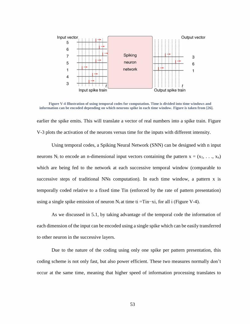
53
earlier the spike emits. This will translate a vector of real numbers into a spike train. Figure
V-3 plots the activation of the neurons versus time for the inputs with different intensity.
Using temporal codes, a Spiking Neural Network (SNN) can be designed with n input
neurons Ni to encode an n-dimensional input vectors containing the pattern x = (x1, . . ., xn)
which are being fed to the network at each successive temporal window (comparable to
successive steps of traditional NNs computation). In each time window, a pattern x is
temporally coded relative to a fixed time Tin (enforced by the rate of pattern presentation)
using a single spike emission of neuron Ni at time ti =Tin−xi, for all i (Figure V-4).
As we discussed in 5.1, by taking advantage of the temporal code the information of
each dimension of the input can be encoded using a single spike which can be easily transferred
to other neuron in the successive layers.
Due to the nature of the coding using only one spike per pattern presentation, this
coding scheme is not only fast, but also power efficient. These two measures normally don’t
occur at the same time, meaning that higher speed of information processing translates to
Figure V-4 Illustration of using temporal codes for computation. Time is divided into time windows and
information can be encoded depending on which neurons spike in each time window. Figure is taken from [26].

54
higher power consumption through expression 𝑃 = 𝛼 2𝑓 where α is the activation factor, V
is the supply voltage, and f is the frequency of operation. Therefore, being able to do the
computation faster while saving on power is extremely efficient. Other than energy efficiency,
and speed, temporal codes can also open up a whole new range of coding options, many of
which are largely unexplored.
5.3 Time as Basis for Information Encoding
From a combinatorial point of view, using the time of the spikes as information
representation provides a large information capacity, given a small set of spiking neurons. For
instance, consider that a stimulus has been presented to a set of N spiking neurons each of
which spiking a maximum of one spike in a certain time window. As shown in Figure V-5
information can be encoded using different schemes which are explained in detail in [25] and
I will touch upon them below. For each coding scheme introduced, the information capacity is
also calculated.
Figure V-5 Possible neural codes provided by the temporal coding. Figure is taken from [37].
55
Count Code
In this coding scheme, overall number of spikes fired by neurons in a time window are
counted and each input representation will be coded using the number of the neurons which
are fired in that time window. With such a coding scheme, the maximum amount of
information that can be transmitted is equal to log2(N+1) bits, where N is the number of
neurons, since there are only N+1 possible states of the system.
Binary Code
In this coding method, N bits are to encode the input vector, one bit for each neuron. If the
neuron is “active” and emits a spike the corresponding bit is 1 and otherwise is zero. The N
bits can also be justified by considering that since each neuron can have 2 states, the system
can take 2N states which when applied to Shannon Theorem [27], the information capacity,
log2 (2N) will be N bits.
Timing Code
Using “Timing Codes” information is encoded in the precise timing of spikes. Information
encoding capacity in this case depends on the precision of determining the spike time. The
more the precision the more we can distinguish between relatively close spikes and hence the
more the information capacity. If we suppose that spikes can be timed with a precision of 1
ms, the maximum amount of information that could be transmitted in t ms will be N*log2(t)
bits. Such timing based codes are clearly potentially extremely powerful, but have the
drawback that the decoding mechanism would need precise timing evaluations which is rather
computationally expensive.

56
Rank Order Coding (ROC)
Instead of encoding the information in the exact spike time of the neurons, Thorpe et al in
[25] introduced ROC in which information is encoded in the rank of the spikes from neurons.
In this coding scheme, the order of the firing between neurons will encode the input vector.
For example, if we have 3 neurons A, B and C, each permutation of A, B and C will be a new
code. As there are 3! =6 ways of permuting 3 objects, the code space will be:
{ABC, ACB, BAC, BCA, CAB, CBA}
Since there are N! states of the system at each time window for N neurons, the information
capacity of ROC is log2(N!).
So far, we have seen how we can use temporal codes to increase the information
capacity using a fix number of neurons, N. In comparison, timing code and ROC contain a
relatively large coding capacity. In order to decode the information in the time of arrival of the
spike we need a very precise timing resolution. We should also keep in mind that decoding
ROC would also need precise timing since we need to distinguish between the order of spikes.
5.4 Rank Order Code
In order to use ROC to train neural networks, a learning algorithm is needed which
reflects upon the order of neural spiking: 𝛥𝑊 = 𝑓(𝑜𝑟𝑑𝑒𝑟). In other words, when a pattern is
presented to the network of neurons, the weights of the neurons who fire earlier will change
more than the ones who fire later. As a result of that, after training, the earlier spikes carry
more information about the input than the later ones do.

57
Now, consider a case where this coding scheme is employed in some form of unsupervised
learning such as competitive learning. In the unsupervised (clustering) problem, we are given
a training set {x (1), . . ., x(m)}, and want to group the data into a few “clusters.” Classic
competitive learning such as K-means clustering algorithm finds K cluster centroids that
minimizes the distance between data points and the nearest centroid [28]. Simply put, at each
pattern presentation, there is one cluster whose centroid’s distance to the input vector is the
least. The new pattern will be grouped with that cluster and a new centroid will be calculated
for the cluster with the new arrangement.
In the concept of neural networks, each cluster represents a neuron and its centroid which
is the mean of the cluster, is the neuron’s weight vector ∈ Rn × k for an n-dimensional input
vector and k clusters. Every time a new input is fed to the input neurons (𝑈1 and 𝑈2) ( Figure
V-6 ), the most active output neuron is the one whose weight vector is the closest to the input
vector. This algorithm is called the Winner-Takes-All (WTA) algorithm, since one neuron
wins the competition between neurons and takes the input into its cluster. Winning neuron’s
weights adjust themselves in a way to get closer to the new input pattern and include that
pattern in the cluster. In other words, weights are the running average of the input patterns.
Figure V-6 Competitive Learning- Each output neuron represents a cluster. N_A and N_B represent cluster
A and B respectively and WA and WB are the centers of the clusters. Upon the arrival of every input pattern, the
winner neuron’s weights adjust themselves to get closer to the input pattern.
• Given a new input, pickthe most active neuron (“winner takes all”)
one whose weights are Closest to new input
• Update weight vector forthat neuron
𝑊1
New input
Cluster A
Cluster B
2 310 4
2
3
1
0
4
𝑊2
𝑊3
𝑊
𝑊 =𝑊1𝑊2
𝑊 =𝑊3𝑊

58
𝑊 (𝑡) = (∑ 𝑖)1
𝑡= (∑ 𝑖 )
1
𝑡
1
𝑖=1
𝑖=1
=𝑡 1
𝑡∗ 𝑊 (𝑡 1)
𝑡
= 𝑊 (𝑡 1) 1
𝑡( 𝑊 (𝑡 1))
→ 𝛥𝑊 = 휀( 𝑊)
where 휀 is the learning rate [29].
Now, let us apply K-means algorithm to Spiking Neural Networks (SNN) and specifically
to Rank Order Code (ROC). Under the presentation of each input vector, there is one neuron
whose weight vector is closest to the input vector resulting in the strongest input and hence the
earliest spike emission. Lateral inhibition can be employed as a means to implement Winner-
Takes-All such that the first spike at the output layer inhibits all the other neurons and will be
the winning neuron whose weights are going to change towards the input. This way, each
neuron will be trained to respond to a specific pattern. For example, in a work done by Rudy
Guyonneauet al in 2004 they train 4 neurons using the rank order code in a spiking neural
network to cluster 4 different images [30]. As is shown in Figure V-7, at the end of the training
set they were able to get each neuron to respond to a specific image from the training set.

59
Hence by using Winner-Takes-All and Rank Order Coding, 4 neurons can encode 4
images. However, as we mentioned in the previous section, 4 neurons using rank order code
have the potential of encoding 4!=16 different input vectors and by applying Winner-takes-all,
this coding space is being wasted and not used to its full potential.
Moreover, a greedy algorithm like WTA combined with Hebbian learning puts the system
in a positive feedback loop driving the weights to one or zero which can be digitally stored.
Digital weights have the advantage of being more robust and immune to noise but are losing a
lot of information in digitization. However, we want to explore the true analog computation
and study the power of computation using analog memory which brings us to the concept of
Winners-Share-All.
5.5 Winners-Share-All (WSA)
Instead of forcing the network to have only one winner for each time window which wastes
the code space, I propose to have multiple winners at the presentation of each input. Then the
question arises: How many winners are enough? In ROC I explained that the earlier rank spikes
Figure V-7 Emergence of selective responses of each neuron to a specific pattern. Lateral inhibition is applied as
a winner takes all mechanism and competitive learning results in the assignment of each pattern to the emission of
one spike from one neuron. Figure is taken from [30].

60
have a lot more information about the input scene that the later ones do. So how many of them
should we keep?
Let us imagine we have n output neurons from which k are firing. The total amount of
information capacity of this arrangement is then 𝑙𝑜𝑔2( 𝑘). To maximize this information
capacity, k should be n/2. Therefore, from a combinatorial point of view, if we enforce the
network to fire half of its output neurons in a time window, we will increase the information
capacity by:
α = log2(
nn2)
log2 .
To get a sense of how much increase this is, for n=10, α 2.4, for n=100 α= 14.5 and for
n=1000 α=100. Thus as the number of neurons at the output grow, the increase in the
information capacity becomes more apparent.
Figure V-8 Comparison of the number of output neurons required to recognize patterns between WTA (blue)
and WSA (red) mechanism. As the number of patterns increase, the efficiency of using WSA becomes more apparent.

61
To highlight yet another advantage of this algorithm, we can compare the number of neurons
needed in order to classify P numbers of patterns with WSA vs WTA. Figure V-8 depicts this
comparison. Using WTA, the number of output neurons required for classification grows
linearly with the number of patterns at the input. However, using WSA, number of neurons
needed undergoes a logarithmic compression and for large number of patterns the gap between
the number of output neurons in WTA vs WSA algorithm increases by a lot.
Although this algorithm is providing us with a lot more information capacity, it’s still lower
than ROC (log2 𝑛! 𝑣𝑠 log2( 𝑘). However, it should be noted that training networks with ROC
is much harder than the proposed scheme. Why?
Consider the case below with 6 output neurons where there are two cases with the same
order of spiking pattern except for the 5th and the 6th neuron (. Basically, in one case we have
the code: 1>2>3>4>5>6 and in the other case, we have: 1>2>3>4>6>5. Although these two
codes are different, they cannot be used to encode two different objects at the input. Why?
Since earlier-rank neurons provide a lot more information about the patterns than the later ones
do, these two rank orders are very similar and cannot be used to encode two different patterns.
Figure V-9 The case with two similar rank codes in which only the rank of two last spikes are different.
1
2
3
4
5
6

62
In other words, the “least-significant-bits (LSBs)” don’t contain much information about the
input and can be ignored in the coding process. This will result in using only the “Most
Significant Bits (MSBs)” or in other words, only half of the neurons which is what WSA is
proposing.
In the next chapter, I will explain how this idea can be used to perform computation in the
form of pattern recognition.

63
VI. Chapter 6: Applying WSA to a Classification Problem
In order to show the power of this algorithm in practice, I applied it to a neural network to
perform a rather small classification problem in which 14 patterns of English Alphabets are to
be clustered with 6 neurons. If we were to use the Winner-Takes-All algorithm on this problem,
we would need 14 neurons at the output. With Winners-Share-All, using only 6 output neurons,
we should be able to classify (63)=20 patterns. Figure VI-1 shows the training set and the test
set patterns chosen for this experiment. The set consists of images of the patterns with the size
15 pixels x 15 pixels and the last column of the training set shows the ideal, non-noisy patterns.
The rest of the patterns are made by flipping 10 pixels either on the pattern or in a neighborhood
Figure VI-1 Training set and Test set patterns used for the classification problem.
Training Set Test Set

64
of one pixel around the pattern inside the image. The reason for generating the noisy patterns
this way is because if we flip the pixels somewhere in the corner of the image, it does not
perturb the pattern at all and hence is very close to the ideal image. Using this method, 5 noisy
versions of each pattern are generated for training and 2 of them are made for testing in order
to evaluate how well the network “generalizes”. The concept of generalizing in machine
learning is referred to how well a neural network classifies the patterns it has not seen before.
A neural network that clusters the patterns well only when it has been presented with it before
is only memorizing the patterns rather than learning them. Hence, it’s very important to
measure the accuracy of the classification done by the network using the test set.
6.1 Network Architecture
The network architecture used here is structured in a similar manner to hierarchical neural
models, specifically to Convolutional Neural Networks (CNNs). A Convolutional Neural
Network (CNN) is comprised of one or more convolutional layers (often with a subsampling
step) and then followed by one or more fully connected layers as in a standard multilayer neural
network. The architecture of a CNN is designed to take advantage of the 2D structure of an
input image (or other 2D input such as a speech signal). This is achieved with local connections
and tied weights followed by some form of pooling which results in translation invariant
features. Another benefit of CNNs is that they are easier to train and have many fewer
parameters than fully connected networks with the same number of hidden units [31].
Figure VI-2 shows the full neural network architecture used in this work.
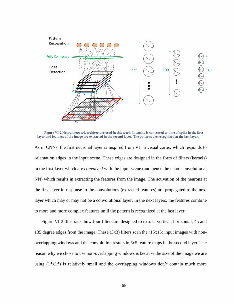
65
As in CNNs, the first neuronal layer is inspired from V1 in visual cortex which responds to
orientation edges in the input scene. These edges are designed in the form of filters (kernels)
in the first layer which are convolved with the input scene (and hence the name convolutional
NN) which results in extracting the features from the image. The activation of the neurons at
the first layer in response to the convolutions (extracted features) are propagated to the next
layer which may or may not be a convolutional layer. In the next layers, the features combine
to more and more complex features until the pattern is recognized at the last layer.
Figure VI-2 illustrates how four filters are designed to extract vertical, horizontal, 45 and
135 degree edges from the image. These (3x3) filters scan the (15x15) input images with non-
overlapping windows and the convolution results in 5x5 feature maps in the second layer. The
reason why we chose to use non-overlapping windows is because the size of the image we are
using (15x15) is relatively small and the overlapping windows don’t contain much more
Figure VI-2 Neural network architecture used in this work. Intensity is converted to time of spike in the first
layer and features of the image are extracted in the second layer. The patterns are recognized at the last layer.
Edge Detection
PatternRecognition
Fully Connected
15
15
5
5
225 100 6

66
information than the non-overlapping ones. The limiting factor in the size of the images is the
processing power causing simulation times to be very large for larger images and hence making
the process of design very tedious. Each “feature map” in the second layer contains a certain
edge. The neurons on the same coordinates on the different feature maps have the same
receptive field on the input image meaning they get their inputs from the same part of the
image.
As is depicted in Figure VI-2, the third layer is combining the features from the second
layer in a fully connected manner to recognize the images on the output layer. This layer is
trained in a completely unsupervised fashion using Spike Timing Dependent Plasticity
(STDP).
The spiking neural network is coded and simulated in MATLAB. Neurons and synapses
are modeled mathematically and are discussed below. The rest of the details of the network
will be discussed later in the chapter.
6.1.1 Neuron’s Model
A leaky integrate and fire model is chosen for the neurons as is defined mathematically as:
𝑚𝑒𝑚(𝑡) = ∫ (𝐼𝑛𝑝 𝑡 𝑃𝑊𝑀(𝑡) 𝛼 𝑚𝑒𝑚(𝑡))𝑑𝑡 𝑇
( 1)𝑇
𝑛 = 𝑓𝑙𝑜𝑜𝑟(𝑡
𝑇)
Where T is the clock period for presenting patterns and is chosen here as 10m sec. α is
the leak coefficient and Input_PWM is the pulse width modulation of the input spikes at each
layer. This modulation keeps the pulses high until the end of the window. Pulse width
modulation weights the spikes who come early more than the ones who come later. As we have
discussed before, in temporal codes the spikes which are emitted first contain more information

67
about the input than the later ones. Therefore, since we are utilizing multiple spikes at each
layer (WSA) we need to weight them differently based on the time of the arrival. Figure VI-3
illustrates this idea. As is shown, the neuron integrates the area under the product of the weight
by the pulse width modulated input. Therefore, the earlier the spikes arrives from the previous
layer, the larger the area under the curve and the more it triggers the neuron in the next layer.
At the end of the time window the pulse width modulation and the membrane potential are
reset to zero and the neuron awaits the next input pattern:
𝑃𝑊𝑀(𝑛𝑇) = 0
𝑚𝑒𝑚(𝑛𝑇) = 0
𝑛 = 0 1 … 𝑓𝑙𝑜𝑜𝑟 (𝑡
𝑡𝑒 )
Where tend is the length of the simulation.
6.1.2 Synapse Model
The connection between the neurons are modeled as a single variable whose value changes
based on dwp (positive changes of w) and dwn (negative changes of w) such that:
𝑤(𝑡 𝑑𝑡) = 𝑤0(𝑡) 𝛽 (𝑑𝑤𝑝(𝑡) 𝑑𝑤𝑛(𝑡)) 𝑓(. )
Figure VI-3 Pulse Width Modulation (PWM) of the pre synaptic input spike in order to weight the earlier spike
more than the later ones. The neuron integrates the dotted green area under the PWM signals and hence the earlier
signals stimulate the neurons more effectively.
Pre1
Pre2
PWM1
PWM2
W1
W2

68
Where β will scale the changes of w and f(.) contains the dynamics of the synapses which
will be discussed in section 6.4.
In the following sections of this chapter I will go through the details of the design choices
and output of each layer.
6.2 Layer 1: Converting Pixel Intensity into Spikes
As I discussed before, in temporal codes each input is presented in a time window and the
information about the input is converted into spike times. As is shown in Figure VI-4a, in layer
1, each neuron is assigned to a pixel whose normalized intensity is given as an input to the
neuron. Pixels refresh their values every 10 ms which is the length of the time bin in which the
network processes each pattern. In other words, the normalized pixel intensity is presented at
the beginning of the time window and is kept constant until the end of the time window. The
input images are normalized by the number of “on” pixels so that if an input pattern has
intrinsically more number of black pixels than others, it will not cause stronger stimulus for
the next layer and all patterns have the same total drive for the following neural layer since
they are scaled by the total number of “on” pixels in the image.
Note that input patterns are shuffled randomly and then given to the input neurons every
10 milliseconds. The reason why is if the data is given in some meaningful order, this can bias
the network and lead to poor convergence and generally a good method to avoid this is to
randomly shuffle the data prior to each epoch of training.

69
Raster plot in Figure VI-4b shows the spike times of the 225 neurons in the first layer.
Figure VI-4c depicts the zoomed version and illustrates the firing of each neuron in every time
bin (10 ms). The neurons containing a black pixel (with a white background) in the pattern
presented at each time bin are the ones who emit a spike.
6.3 Layer 2: Extracting features from the Images
In the field of image processing appropriate filters are applied to an image in order to
extract certain features from it through convolving these filters with each patch of the image.
In the concept of neural networks, this translates to neurons whose weight vectors act as the
filters and whose receptive field act as the input patch. As a result of that, the output of the
neuron is the convolution (product of sum) of the input image patch with the filters defined by
the neurons’ weight vector.
The filters I have chosen at the second layer of the neural network for feature detection are
vertical, horizontal, 45 and 135 degree edges. The weights (synapses) of these filters are non-
Figure VI-4 First layer: converting pixel intensity to spikes. Normalized patterns are presented to the network
every 10 ms and in that time window network processes these patterns. a) Each neuron is assigned to one pixel. b)
Raster plot showing the spiking of 225 neurons in the simulation time. c) zoomed version of the raster plot showing
the spiking of neurons in each 10ms time window in which the patterns are presented.
Time Window
225Neurons
a b c

70
plastic and are hardwired in the program. As is illustrated in Figure VI-5 a, every 9 neurons
from the first layer are representing a 3x3 patch from the image and connect to 4 neurons in
the second layer. These 4 neurons receive spikes from the first layer and depending on the
dominant features of that patch, the corresponding neurons fire. Since the image is 15 x15 and
the receptive fields of each group of 4 neurons are of the size 3x3 and are non-overlapping, the
second layer needs 4 ∗ (15
3) ∗ (
15
3) = 100 neurons. Neurons 1-4 correspond to the left corner
of the image and neurons 5-8 correspond to the window just to the right of that and so on and
so forth. In each time bin of 10 ms where a new pattern is presented, spikes from the first layer
travel through the second layer and the neurons corresponding to the dominant edges of that
pattern spike. This can be observed in Figure VI-5 b with the highlighted time window. Figure
VI-6 c depicts the raster plot of the 100 neurons in the second layer in 10000 seconds.
Figure VI-5 Second layer: extracting edges from each kernel. 3x3 kernels are taken from the image and are
convolved with features that are hardwired in the network. This layer of neurons responds to dominant edges existing
in each 3x3 kernel.
Time Window
225Neurons
100Neurons
a) b) c)

71
6.4 Layer 3: Classification
The third layer in this convolutional neural net is fully connected to the feature extraction
layer. Our goal here is to train these connections in an unsupervised fashion to classify 14
patterns shown in Figure VI-1 using spike combinations of 6 output neurons. In this spiking
neural network, Spike Timing Dependent Plasticity is used to modify weights and in this
section I’ll explain the details of the learning and the challenges while training this spiking
neural network with Winner-Shares-All algorithm in a completely unsupervised fashion.
6.4.1 Challenge 1: Learning
a) Positive Weight Change
As explained before, during each time bin, the neuron which spikes earlier carries the most
amount of information about the input and in order to incorporate that in the model, I use pulse
width modulation to the input spike which results in longer stimulation of post-synaptic
neurons from the pre-synaptic spikes arriving earlier.
To reflect this in the learning algorithm:
i) The pre-synaptic spikes arriving earlier and causing the post synaptic neuron to fire
should undergo a larger weight change than the ones who helped with the
stimulation but arrived later.
ii) ii) Moreover, I introduce an intermediate parameter C inspired by the calcium
concentration and its role in learning. This value increases with the arrival of the
pre-synaptic spike at the synaptic joint and decays over time in the form of 𝑐(𝑡) =
𝑒 𝑎( 𝑠𝑝𝑖𝑘𝑒). When the post-synaptic spike occurs, it samples this parameter at the
time of its firing and the synaptic change will be directly proportional to this value.

72
Now, combining the two aforementioned ideas, the C parameter should increase in the
form of 𝑐′(𝑡) = 1 𝑒 𝑎( 𝑠𝑝𝑖𝑘𝑒) when a pre spikes happens, so that it can incorporate the
effect of early versus later spikes. Therefore, the later spikes have a lower value of C in
comparison with the earlier spikes and hence their corresponding weights undergo a smaller
weight change. Basically, this learning algorithm is a form of anti-STDP rule within the time
bin, because the weight change will be greater as the pre spike emits earlier in time (within the
time bin) with respect to the post spike. This is desirable since the weight change reflects the
mutual information between the pre and the post synaptic neurons which is encoded in the time
of arrival of the spikes.
The learning algorithm is shown graphically in Figure VI-7a and can be described
mathematically as:
𝑐(𝑡) = ∫(𝛿(𝑡 𝑡 𝑒) 𝛼 ∗ 𝑐(𝑡)) 𝑑𝑡
𝑐′(𝑡) = (𝑡 𝑡 𝑒) 𝑐(𝑡)
𝑑𝑤𝑝 = 𝐿𝑅𝑎 𝑒𝑃 ∗ 𝛿(𝑡 𝑡 𝑜𝑠 ) ∗ 𝑐′(𝑡) = 𝐿𝑅𝑎 𝑒𝑃 ∗ 𝑐′(𝑡 𝑜𝑠 )
Where dwp is the positive weight change and LRateP is the positive learning rate.
b) Negative Weight Change
When there is no correlation between a pre-synaptic and a post-synaptic neuron the
connection between them undergoes a negative weight change. This lack of correlation
translates to the post-synaptic neuron firing before the pre-synaptic counterpart. The later the

73
pre-synaptic neuron spikes with respect to the post synaptic neuron (within a time bin), the
more uncorrelated the two neurons are. Hence, the same anti-STDP rule applies here.
Note that the weight could also endure a negative change when there is no correlation
whatsoever between the pre and post; meaning that the pre-synaptic neuron does not emit any
spike within the time bin while the post has spiked. In that case the negative weight change is
maximum. This is described graphically in Figure VI-7b and can be written mathematically
as:
𝑐(𝑡) = ∫(𝛿(𝑡 𝑡 𝑜𝑠 ) 𝛼 ∗ 𝑐(𝑡)) 𝑑𝑡
𝑐′(𝑡) = (𝑡 𝑡 𝑜𝑠 ) 𝑐(𝑡)
Figure VI-7 Spiking learning algorithm developed for WSA. Calcium concentration models are used as part of
the Anti-STDP rule to calculate dwp and dwn.
S
R
Q
Qb
Pre
C(t) C’(t) x
Post𝑡 𝑜𝑠
𝑡 𝑒
x
LRateP
dwp
a)
b)
S
R
Q
Qb
Post
C(t) C’(t) x
Pre𝑡 𝑒
𝑡 𝑜𝑠
x
x
LRateN
dwn

74
𝑑𝑤𝑛 = 𝐿𝑅𝑎 𝑒𝑁 ∗ (𝛿(𝑡 𝑡 𝑒) ∗ 𝑐′(𝑡) 𝑝𝑟𝑒 𝑑𝑜𝑒𝑠𝑛𝑡 𝑠𝑝𝑖𝑘𝑒 ∗ 𝛿(𝑡 𝑡 𝑜𝑠 ))
= 𝐿𝑅𝑎 𝑒𝑁 ∗ 𝑐′(𝑡 𝑒)
Where dwn is the negative weight change and LRateN is the negative learning rate.
6.4.2 Challenge 2: Inhibition
As I argued in chapter 5, Winners-Share-All algorithm requires only half of the neurons at
the output to fire. In order to enforce this requirement, we need to ensure that:
a) No neuron fires more than once in a specific time window.
b) With 6 output neurons, upon the arrival of the third spike, all other neurons need to
be inhibited.
Figure VI-8 shows the solutions employed to establish the above conditions. A self-
inhibitory connection at each output neuron ensures that no neuron spikes more than once in
any given time window since the neuron undergoes an inhibition upon spiking (condition a).
The inhibitory neuron in Figure VI-8 accumulates the spikes emitted from the pool of the
output neurons and its threshold is set so that it fires after the third spike has been generated
hence inhibiting all the neurons at the output (condition b). We can model the inhibitory neuron
with the following mathematical expression:
𝑚𝑒𝑚𝑖𝑛ℎ𝑖𝑏𝑖𝑡(𝑡) = ∫ (𝑆𝑝𝑖𝑘𝑒𝑠𝑙𝑎𝑦𝑒 3 𝛼𝑖 ℎ𝑖𝑏 ∗ 𝑚𝑒𝑚 𝑖 ℎ𝑖𝑏𝑖 (𝑡))𝑑𝑡
( 1)𝑇
(𝑛 1)𝑇 < 𝑡 < 𝑛𝑇
𝐼𝑛ℎ𝑖𝑏𝑖𝑡 = {1 𝑚𝑒𝑚 > ℎ 𝑖 ℎ𝑖𝑏𝑖 0 𝑂𝑡ℎ𝑒𝑟𝑤𝑖𝑠𝑒
𝑚𝑒𝑚 𝑖 ℎ𝑖𝑏𝑖 (𝑛𝑇) = 0
𝑛 = 0 1 … 𝑓𝑙𝑜𝑜𝑟 (𝑡
𝑡𝑒 )

75
And therefore each output neuron i can be described as:
𝑚𝑒𝑚𝑜𝑢𝑡𝑖 (𝑡) = ∫ (𝑆𝑝𝑖𝑘𝑒𝑠𝑙𝑎𝑦𝑒 2 𝛼𝑙𝑒𝑎𝑘 ∗ 𝑚𝑒𝑚𝑜𝑢𝑡
𝑖 (𝑡) 𝐼𝑛ℎ𝑖𝑏𝑖𝑡 𝛿(𝑡 𝑡𝑠 𝑖𝑘𝑒𝑖
( 1)𝑇
)) 𝑑𝑡
(𝑛 1)𝑇 < 𝑡 < 𝑛𝑇
Where 𝑚𝑒𝑚𝑜𝑢𝑡𝑖 refers to the ith. output neuron membrane potential and 𝛿(𝑡 𝑡𝑠 𝑖𝑘𝑒𝑖) is the
spike emitted from the same output neuron which represents self-inhibition employed to ensure
the neuron does not spike more than once in any given time window.
6.4.3 Challenge 3: Correlation in the input patterns
In this problem we have a set of synthetic and relatively small images which results in high
correlation between pixels. Hence, there is similarities between the patterns which makes it
more likely for different patterns to be recognized as a single one and therefore it’s challenging
to separate them as different classes. The solution I employed for this problem is what I call
habituation because it diminishes the innate response of the neurons to a frequently repeated
stimulus. In habituation, the network finds the similarities between the patterns and ignore
Figure VI-8 Inhibitory neuron designed to ensure not more than half of the output neurons fire at any given time
window.
𝐼𝑛ℎ𝑖𝑏𝑖𝑡 = ∫(𝑆𝑝𝑖𝑘𝑒𝑠𝑙𝑎𝑦𝑒 3 α𝑖 ℎ𝑖𝑏 ∗ 𝐼𝑛ℎ𝑖𝑏𝑖𝑡)
ℎ 𝑖 ℎ𝑖𝑏𝑖
Inhibitory LIF Neuron

76
them and instead looks for dissimilarities. This is illustrated in Figure VI-9. An intermediate
habituation leaky integrate and fire neuron is introduced between each neuron in layer 2 and
layer 3. It receives its input from the neuron in layer 2 and its output spikes modifies the
connection between the corresponding neurons in layer 2 and layer 3. The threshold of this
habituation neuron is set so that it can detect the frequent firing of its input neuron in layer 2.
The frequent firing of such neuron identifies a common feature in that specific location on the
image. Information theoretically, that feature contains very little information about the pattern
since it’s very probable to happen and therefore has a low entropy and can be ignored.
The habituation neuron can be defined as:
𝑚𝑒𝑚 ℎ𝑎𝑏𝑖 (𝑡) = ∫ (𝑆𝑝𝑖𝑘𝑒𝑠𝑙𝑎𝑦𝑒 2 𝛼ℎ𝑎𝑏 ∗ 𝑚𝑒𝑚 ℎ𝑎𝑏𝑖 )𝑑𝑡
0
ℎ𝑎𝑏𝑖𝑡 = {1 𝑚𝑒𝑚ℎ𝑎𝑏𝑖𝑡 > ℎℎ𝑎𝑏𝑖𝑡0 𝑂𝑡ℎ𝑒𝑟𝑤𝑖𝑠𝑒
Note that unlike other neurons that we have so far introduced, the habituation neuron does
not reset at the end of the time window since it has to keep the history of the patterns. It only
Figure VI-9 Habituation neuron designed to ignore the similarities between the input patterns and look for the
differences between patterns which helps to separate patterns.
𝑖
𝑊𝑖
ℎ𝑎𝑏
ℎ𝑎𝑏𝑖𝑡 𝑎𝑡𝑖𝑜𝑛 = ∫(𝑆𝑝𝑖𝑘𝑒𝑠𝑙𝑎𝑦𝑒 2 αℎ𝑎𝑏 ∗ ℎ𝑎𝑏𝑖𝑡 𝑎𝑡𝑖𝑜𝑛)
Vth

77
resets when it reaches the threshold and fires a spike. The modification of weight due to
habituation is modeled below:
𝑑𝑤𝑖 = 𝛼 (𝑑𝑤𝑝𝑖 𝑑𝑤𝑛𝑖 ) 𝛽 ∗ 𝛿(𝑡 𝑡ℎ𝑎𝑏𝑖 𝑖 ) ∗ 𝑒𝑥𝑝 ( 𝛾𝑡)
where dwpij and dwnij are the positive and negative changes of weight due to STDP between
neurons i,j in layer 2 and 3 which I explained in section 6.4.2. 𝛿(𝑡 𝑡ℎ𝑎𝑏𝑖 𝑖 ) are the spikes
from the habituation neuron which are decreasing the weight between neurons i and j as
discussed above. However, there is an exponential decay associated with the habituation since
as the network learns the input data the effect of it should become less and less in order to
encourage convergence. This works similar to the heuristics generally applied to learning rate
in neural network in order to achieve convergence faster.
6.4.4 Challenge 4: Greedy Attractor
a) Homeostatic Plasticity
Neuronal activity is the key to learning by the changes of synaptic connectivity through the
‘Hebbian’ mechanism or in the spike form, ‘Spike Timing Dependent Plasticity (STDP)’.
However, STDP is a non-controlled growth or decay of synaptic ‘weights’ and hence, a
destabilizing force in neural circuits. For example, in the context of WSA algorithm, if one
combination starts off being favorable for multiple patterns, hebbian based learning will
encourage that behavior (since it’s a positive feedback mechanism) and the weights run off to
the extremes and hence lose a lot of information.

78
One proposed idea to solve this problem is that the average neuronal activity is maintained
within a range by homeostatic plasticity mechanism which dynamically adjust synaptic
strength in the correct direction to promote stability [32].
The authors in [32] argue that the data from in vitro cortical networks indicate that
homeostatic synaptic plasticity rules independently adjust excitatory and inhibitory feedback
loops within recurrent cortical networks so that activity is preserved despite change in drive.
When activity falls too low (because, for example, sensory drive is reduced), excitation
between pyramidal neurons is boosted and feedback inhibition is reduced ( Figure VI-10 ).
This should raise the firing rates of pyramidal neurons. Conversely, when activity is too high,
excitation between pyramidal neurons is reduced, and excitation onto interneurons and
inhibitory inputs back onto pyramidal neurons are increased, thereby boosting feedback
inhibition. This should lower the activity of pyramidal neurons. So, homeostatic regulation of
network activity in recurrent cortical circuits is accomplished through a coordinated set of
changes that selectively adjust different classes of synapse to drive network activity towards
some set point.
Figure VI-10 Concept of homeostatic plasticity in the brain. Feedback mechanisms are applied in order to keep
the firing rate of a neuron in a target range. Figures are taken from [32].

79
Employing homeostatic property has two main advantages:
1) It will not let one output neuron (or in our case one combination) get very greedy and
respond to many input patterns. In other words, it will “watch” the competition and
make sure all the combinations will get a chance to respond to some input pattern.
2) It will also act as a regularizer for the neural network to avoid overfitting. Overfitting
is a concept in machine learning where the network starts fitting too well to the training
set and loses generalization and hence do not do well on the testing set. In this case
network parameters start changing because of the “noise” in the data set and have a
poor performance in recognizing patterns that have not been presented to it before.
Regularization will make sure to control the growth of the weights in a way that the
network response to small random variations in the input is minimal which is also what
the homeostatic property is doing.
b) Homeostatic Plasticity in action
To dynamically adjust synaptic strength in the correct direction to promote stability in the
weights, we need to first identify the greedy behavior in neurons. Therefore, we need a type of
“Neural State Machine (NSM)” to recognize if a neural state is happening too often or too
rarely. Figure VI-11 illustrates this idea. Each neuron in the state machine is assigned to
respond to the advent of a certain combination or state. Since we have enforced the condition
of a maximum number of 3 (half of the output neurons) to fire at every time bin, then every
neuron in the state machine takes input from 3 neurons which make a unique combination. The
leaky integrator and fire neuron is designed to fire after detecting the 3 neuron firing at its
input. As a result of that at each time window, the spikes out of the neural state machine

80
indicate the combination that has occurred. The inset in Figure VI-11 depicts the detection of
the combination 1,2,3 from the first neuron in the NSM.
Now, to find out if a combination is happening too often or too rare and correct it, we feed
the spikes from the neural state machine with detected combinations to a block with leaky
integrator units. The time constant of these leaky integrators are a design choice and has to be
picked in order to determine what it means to be too often or too rare depending on the network
behavior. Each leaky integrator (LI) parameter keeps the history of every combination
occurrence and if it’s greater than a certain threshold of Vth,p it generates a spike which
translates to that combination being happening too often. On the contrary, if the LI parameter
goes below a threshold of Vth,n, a spike will be generated which means that the combination is
dormant and is taking place too rare.
This can be mathematically described as below:
Figure VI-11 Neural State Machine (NSM) designed to control the appearance frequency of the WSA codes.
NeuralState
Machine
1
2
3
4
5
6
1
2
3
4
5
6Combination 1 (1,2,3)
DetectionSpike
Combination 20 (4,5,6) Detection
Spike
CombinationToo Frequent Spike
∫
ℎ
ℎ
∫
ℎ
ℎ
0.75
0.75
CombinationToo Rare Spike
Summing element:ORING combinations including neuron 1-6
SummingToo Frequent Spike
SummingToo RareSpike
Leaky Integrate ElementsTaking track of how much the threshold of the associated neuron has to change
ℎ
ℎ

81
𝑚𝑒𝑚𝑁𝑆𝑀𝑖 (𝑡) = ∫ ( ∑ 𝛿 (𝑡 𝑡𝑠 𝑖𝑘𝑒 ) 𝛼3 ∗ 𝑚𝑒𝑚𝑁𝑆𝑀
𝑖 (𝑡)) 𝑑𝑡
𝑘3𝑖
=𝑘1𝑖
( 1)𝑇
(𝑛 1)𝑇 < 𝑡 < 𝑛𝑇
𝑘1𝑖 𝑘 𝑖 𝑘3𝑖 ⋲ { uro th th om t o }
𝑆𝑝𝑖𝑘𝑒𝑁𝑆𝑀𝑖 = {
1 𝑚𝑒𝑚𝑁𝑆𝑀𝑖 > ℎ 𝑁𝑆𝑀
0 𝑂𝑡ℎ𝑒𝑟𝑤𝑖𝑠𝑒
𝐿𝐼𝐶𝑜𝑚𝑏𝑖 (𝑡) = ∫ (𝑆𝑝𝑖𝑘𝑒𝑁𝑆𝑀𝑖 𝛼2 ∗ 𝐶𝑜𝑚𝑏𝐹𝑟𝑒𝑞𝐷𝑒𝑡
𝑖)𝑑𝑡
0
𝐶𝑜𝑚𝑏𝐹𝑟𝑒𝑞𝐷𝑒𝑡𝑖 (𝑡) = 𝐿𝐼𝐶𝑜𝑚𝑏𝑖 (𝑡) 𝜉
Where ξ is a positive bias added to the output of the integrator as a DC shift in order to
detect the non-spiking combination through the decay parameter going below the low
threshold:
𝐶𝑜𝑚𝑏𝑇𝑜𝑜𝑂𝐹𝑡𝑒𝑛 = {1 𝐶𝑜𝑚𝑏𝐹𝑟𝑒𝑞𝐷𝑒𝑡 > ℎ
0 𝑂𝑡ℎ𝑒𝑟𝑤𝑖𝑠𝑒
𝐶𝑜𝑚𝑏𝑇𝑜𝑜𝑅𝑎𝑟𝑒 = {1 𝐶𝑜𝑚𝑏𝐹𝑟𝑒𝑞𝐷𝑒𝑡 < ℎ 0 𝑂𝑡ℎ𝑒𝑟𝑤𝑖𝑠𝑒
We can now use the information from the combination occurrence frequency in order to
correct the direction of network convergence to promote stability. One way of doing so which
is inspired by the work in [33] is to use each “too often spikes (TOS)” to increase the threshold
of the neurons in the combination and to use each “too rare spike (TRS)” to decrease the
threshold of the corresponding neurons. Increasing the threshold decreases the activity of the
neurons and decreasing it increases their activity so it will put the system in a negative feedback
loop which controls the combination frequency within a range as was discussed in the part a
of this section (Figure VI-11 ). The OR gates in the figure are used to shrink the outputs from

82
the number of combinations to the number of output neurons. jth OR at the top is summing the
TOS including neuron j and ith OR at the bottom is doing so for TRS including neuron i.
However, since we were dealing with combinations of neuron firing here, a neuron might
be contributing in TOS at the same time as it is doing so for TRS. To make that clear let me
give an example. If combination “1,2,3” is happening too often and “1,4,6” is not being seen
at all, then neuron 1’s threshold should increase because of the TOS and also decrease because
of TRS. Therefore, we need an averaging mechanism to determine how the threshold of each
neuron has to change on average. That can be achieved by using another set of integrators
which keep track of the history of TOS and TRSs. This is illustrated graphically in Figure
VI-11. The output of these averaging neurons are used to modify the threshold of the output
neurons with a feedback shown in green in the Figure.
𝐴𝑣𝑒𝑟𝑎𝑔𝑒𝑟𝑃𝑖(𝑡) = ∫ (∑(𝐶𝑜𝑚𝑏𝑇𝑜𝑜𝑂𝑓𝑡𝑒𝑛 ) 𝛼3 ∗ 𝐴𝑣𝑒𝑟𝑎𝑔𝑒𝑟𝑃
𝑖(𝑡))𝑑𝑡
0
𝐴𝑣𝑒𝑟𝑎𝑔𝑒𝑟𝑁𝑖 (𝑡) = ∫ (∑(𝐶𝑜𝑚𝑏𝑇𝑜𝑜𝑅𝑎𝑟𝑒 ) 𝛼3 ∗ 𝐴𝑣𝑒𝑟𝑎𝑔𝑒𝑟𝑁
𝑖 (𝑡))𝑑𝑡
0
𝑗 ⋲ {𝑎𝑙𝑙 𝑐𝑜𝑚𝑏𝑖𝑛𝑎𝑡𝑖𝑜𝑛𝑠 𝑖𝑛𝑙 𝑑𝑖𝑛𝑔 𝑡ℎ𝑒 𝑖 ℎ𝑛𝑒 𝑟𝑜𝑛}
ℎ𝑖 (𝑡) = ℎ0 𝛽1 ∗ 𝐴𝑣𝑒𝑟𝑎𝑔𝑒𝑟𝑃
𝑖(𝑡) 𝛽2 ∗ 𝐴𝑣𝑒𝑟𝑎𝑔𝑒𝑟𝑁𝑖 (𝑡)

83
6.5 Results
6.5.1 Weight Evolution
Weights of the output neurons are initialized using normal distributed random numbers.
The mean is chosen to be small since we have noticed by choosing large means closer to 1, the
weights get saturated very fast and learning stops. The standard deviation of the normal
distribution has to be chosen large enough to separate the weights sufficiently in the beginning
but also not so large that the weights saturate. After 140 epochs of training, looking at the
weight evolution of the connections to layer 3 as is shown in Figure VI-12, it’s apparent that
they take analog values between zero and one. The weights don’t run off to the maximum and
minimum and maintained in the analog region by the negative feedback mechanisms employed
in the network. These analog weights provide us with a lot more information capacity to encode
the input scene.
Figure VI-12 Weight evolution showing the weights converging to analog values.

84
6.5.2 Output Neurons Output
Let us now look at the output of the network as is depicted in Figure VI-13. In each time
window of 10 ms, the outputs of 6 output neurons are monitored and are shown as raster plots.
But as can be noticed, not all the 3 output neurons fire at all times since we only ensured that
not more than 3 neurons fire, but we never enforced exactly 3 neurons to fire. Moreover, it
seems rather unnatural to force exactly half of the neurons to fire in response to every pattern
and looking at it more carefully, this can potentially increase the code space even more. This
way, in the code space, not only we have combinations of 3 out of 6 neurons firing, but also
we can have combinations of every pair of neurons, and also only one neuron to fire in response
to patterns. This increases the code space for 6 output neurons to:
(6
3) (
6
) (
6
1) = 41
And in a more generalized form for n output neurons to:
Time Window
Not all the 3 spike…
Figure VI-13 Spikes from the output neurons. Zoomed in view is showing that half of the neurons don't necessarily
spike at each clock cycle.
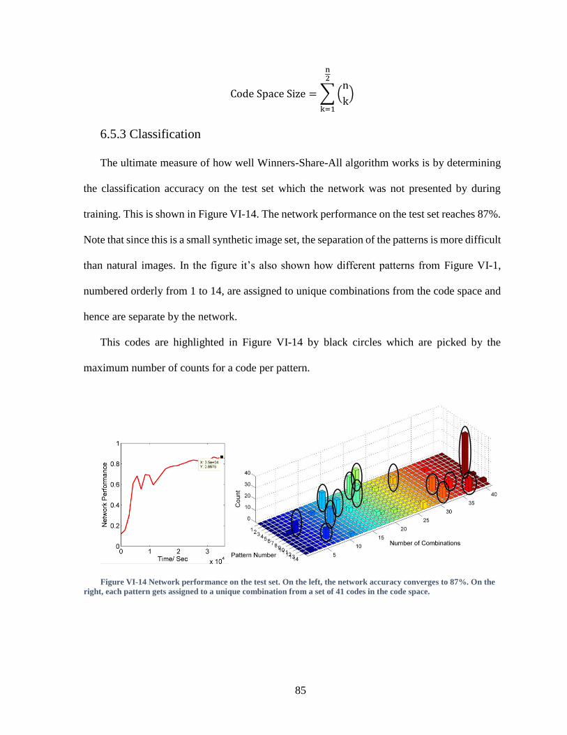
85
Co S S z =∑(
k)
2
k=1
6.5.3 Classification
The ultimate measure of how well Winners-Share-All algorithm works is by determining
the classification accuracy on the test set which the network was not presented by during
training. This is shown in Figure VI-14. The network performance on the test set reaches 87%.
Note that since this is a small synthetic image set, the separation of the patterns is more difficult
than natural images. In the figure it’s also shown how different patterns from Figure VI-1,
numbered orderly from 1 to 14, are assigned to unique combinations from the code space and
hence are separate by the network.
This codes are highlighted in Figure VI-14 by black circles which are picked by the
maximum number of counts for a code per pattern.
Figure VI-14 Network performance on the test set. On the left, the network accuracy converges to 87%. On the
right, each pattern gets assigned to a unique combination from a set of 41 codes in the code space.

86
6.5.4 Discussion
The network starts with a random initial condition and over the course of training picks
certain codes for each pattern. One interesting study is to see if there is any correlation between
the “distance” of the patterns and the “distance” of the codes that are being picked. The former
Figure VI-15 Edit distance vs Pattern similarity for all the patterns.
H F
T L
X Y
k t
M W
S A
n V

87
can be measured by the similarity between the patterns which I’m defining as the number of
common pixels between the patterns while the former is simply the edit distance between the
codes. Edit distance is a way of quantifying how dissimilar two strings are to one another by
counting the minimum number of operations needed to transform one string to the other. For
example, the edit distance between two codes of ‘1,2,3’ and ‘3,4,5’ are 2, since 2 substations
are needed to transform one to the other. For each pattern I plot the edit distance of the code
assigned to it during the simulation versus its similarity to all other patterns. This is shown in
Figure VI-15. The data points are the average of data for 3 initial condition. As can be seen
from the figure, the probability of lower edit distance goes higher as the similarity between the
patterns increases. This can be confirmed in the case where all the pixels are the same (self-
comparison), the code is the same and hence the edit distance is zero. Therefore, the output of
the network, gives us another piece of information other than the recognition, and that is how
similar the patterns are.
88
VII. Conclusion and Future Work
7.1 Conclusion
In this thesis I address the issues that the neuromorphic field faces in terms of number of
connections needed on chip to perform brain-like functions. I explain the two-pronged method
I investigated in order to tackle this problem.
Firstly, the advent of memristors as nano-size devices which can be 3D integrated on top
of CMOS chips guided us through making platforms in the CMOS process to utilize them as
possible memory devices and also as synaptic connections between the CMOS neurons. Two
chips were taped out to explore these possibilities. First chip was realized as a configurable
memory platform designed with the CMOL architecture providing appropriate programming
and sensing circuitry along with the decoding to access the memory cells. This chip was
successfully used by our collaborators for 3D integration and its configurability enabled the
required supporting circuitry for different types of memristors. Second chip was also designed
as a configurable pool of CMOS neurons designed under the CMOL architecture. The CMOS
neurons generate programmable pulse shapes which are engineered to implement online
learning through STDP while driving the memristive crossbar array.
Secondly, by taking advantage of the coding theory, I was able to develop a novel algorithm
to exploit the coding space provided by the spiking neural networks. I introduced the concept
of Winners-Share-All as a replacement for Winner-Takes-All which takes a combinatorial
approach in coding the spikes emitted from the output neurons. By employing this algorithm
less number of neuronal agent is required to perform classification tasks and hence it also
reduces the number of connections and training parameters. In the thesis, I point out the

89
challenges encountered by using this algorithm and how I used a network of recurrent neurons
to overcome them. I used this algorithm to classify 14 artificial images using only 6 output
neurons and achieved a classification accuracy of 87% using a completely unsupervised
approach.
7.2 Future Directions
I used the Winners-Share-All algorithm to classify artificial images. In order to show the
true power of this algorithm, it has to be tested against standard platforms such as the
handwritten digit data set known as MNIST. Similar approaches utilized for the artificially
made data set can be taken for MNIST. Firstly, the features of MNIST images need to be
extracted in the form of filters to be used in a Convolutional Neural Network. This can be done
by training an auto-encoder which is being applied on randomly chosen patches of the MNIST
training data set. The patches need to have the same size as we desire for the filters. The auto-
encoder finds the basis vectors by which the images in the dataset can be defined. Figure
VII-1shows the features extracted from MNIST by training an auto-encoder with a hidden size
Figure VII-1 400 features extracted from MNIST training set by training an autoencoder.

90
of 400 and a visible size of 7x7 which is the size of the patches randomly chosen from MNIST
training set. These filters can then be used to extract the features of every single image in the
training data set which will be transformed in the form of spikes. The last layer of the network
will be identical to the one we used in this thesis.
This coding algorithm could also be expanded to work at every layer. In other words, all
the layers of a deep network can be coded using this algorithm. Doing so will be extremely
efficient in terms of area since the exploitation of the temporal code is being utilized at every
layer and the number of parameters will reduce at each layer by the α parameter of WSA.
91
References
[1] D. Modha, “Introducing a Brain-inspired Computer.” [Online]. Available:
http://www.research.ibm.com/articles/brain-chip.shtml.
[2] B. Linares-Barranco and T. Serrano-Gotarredona, “On the design and characterization
of femtoampere current-mode circuits,” IEEE J. Solid-State Circuits, vol. 38, no. 8,
pp. 1353–1363, 2003.
[3] S. Mitra, S. Fusi, and G. Indiveri, “Real-time classification of complex patterns using
spike-based learning in neuromorphic VLSI,” IEEE Trans. Biomed. Circuits Syst., vol.
3, no. 1, pp. 32–42, 2009.
[4] T. Pfeil, T. C. Potjans, S. Schrader, J. Schemmel, M. Diesmann, and K. Meier, “Is a 4-
bit synaptic weight resolution enough? - constraints on enabling spike-timing
dependent plasticity in neuromorphic hardware,” Front. Neurosci., no. JULY, pp. 1–
19, 2012.
[5] C. Diorio, P. Hasler, A. Minch, and C. a. Mead, “A single-transistor silicon synapse,”
IEEE Trans. Electron Devices, vol. 43, no. 11, pp. 1972–1980, 1996.
[6] R. Serrano-Gotarredona, T. Serrano-Gotarredona, A. Acosta-Jiménez, and B. Linares-
Barranco, “A neuromorphic cortical-layer microchip for spike-based event processing
vision systems,” IEEE Trans. Circuits Syst. I Regul. Pap., vol. 53, no. 12, pp. 2548–
2566, 2006.
[7] K. K. Likharev and D. B. Strukov, “CMOL : Devices , Circuits , and Architectures.”
[8] W. Lu, K. H. Kim, T. Chang, and S. Gaba, “Two-terminal resistive switches
(memristors) for memory and logic applications,” Proc. Asia South Pacific Des.

92
Autom. Conf. ASP-DAC, pp. 217–223, 2011.
[9] J. J. Yang, D. B. Strukov, and D. R. Stewart, “Memristive devices for computing.,”
Nat. Nanotechnol., vol. 8, no. 1, pp. 13–24, 2013.
[10] A. Ghofrani, M. A. Lastras-Montano, and K. T. Cheng, “Towards data reliable
crossbar-based memristive memories,” Proc. - Int. Test Conf., 2013.
[11] M. S. Qureshi, M. Pickett, F. Miao, and J. P. Strachan, “CMOS interface circuits for
reading and writing memristor crossbar array,” Proc. - IEEE Int. Symp. Circuits Syst.,
pp. 2954–2957, 2011.
[12] D. B. Strukov and K. K. Likharev, “CMOL FPGA: a reconfigurable architecture for
hybrid digital circuits with two-terminal nanodevices,” Nanotechnology, vol. 16, no. 6,
pp. 888–900, 2005.
[13] M. A. Lastras-Montano, A. Ghofrani, and K. T. Cheng, “Architecting energy efficient
crossbar-based memristive random-access memories,” Proc. 2015 IEEE/ACM Int.
Symp. Nanoscale Archit. NANOARCH 2015, no. 2, pp. 1–6, 2015.
[14] J. Rofeh, A. Sodhi, M. Payvand, M. A. Lastras-monaño, A. Ghofrani, A. Madhavan,
S. Yemenicioglu, K. Cheng, and L. Theogarajan, “Vertical Integration of Memristors
onto Foundry CMOS Dies using Wafer-Scale Integration,” pp. 1–5.
[15] M. Payvand, A. Madhavan, M. A. Lastras-montaño, A. Ghofrani, J. Rofeh, D.
Strukov, and L. Theogarajan, “A Configurable CMOS Memory Platform for 3D-
Integrated Memristors.”
[16] G. Q. Bi and M. M. Poo, “Synaptic modifications in cultured hippocampal neurons:
dependence on spike timing, synaptic strength, and postsynaptic cell type.,” J.
Neurosci., vol. 18, no. 24, pp. 10464–10472, 1998.

93
[17] T. Chang, S. H. Jo, K. H. Kim, P. Sheridan, S. Gaba, and W. Lu, “Synaptic behaviors
and modeling of a metal oxide memristive device,” Appl. Phys. A Mater. Sci. Process.,
vol. 102, no. 4, pp. 857–863, 2011.
[18] C. Zamarreño-Ramos, L. a. Camuñas-Mesa, J. a. Perez-Carrasco, T. Masquelier, T.
Serrano-Gotarredona, and B. Linares-Barranco, “On spike-timing-dependent-
plasticity, memristive devices, and building a self-learning visual cortex,” Front.
Neurosci., vol. 5, no. MAR, pp. 1–22, 2011.
[19] M. Prezioso, F. Merrikh Bayat, B. Hoskins, K. Likharev, and D. Strukov, “Self-
Adaptive Spike-Time-Dependent Plasticity of Metal-Oxide Memristors,” Sci. Rep.,
vol. 6, no. February, p. 21331, 2016.
[20] M. Prezioso, F. Merrikh-Bayat, B. D. Hoskins, G. C. Adam, K. K. Likharev, and D. B.
Strukov, “Training and operation of an integrated neuromorphic network based on
metal-oxide memristors.,” Nature, vol. 521, no. 7550, pp. 61–4, 2015.
[21] L. Wang and L. Theogarajan, “A micropower delta-sigma modulator based on a self-
biased super inverter for neural recording systems,” Proc. Cust. Integr. Circuits Conf.,
2010.
[22] O. Bichler, D. Querlioz, S. J. Thorpe, J. P. Bourgoin, and C. Gamrat, “Extraction of
temporally correlated features from dynamic vision sensors with spike-timing-
dependent plasticity,” Neural Networks, vol. 32, pp. 339–348, 2012.
[23] M. D. Pardoen and M. G. Degrauwe, “Rail-to-rail input/output CMOS power
amplifier,” IEEE J. Solid-State Circuits, vol. 25, no. 2, pp. 501–504, 1990.
[24] W. S. McCulloch AND W. Pitts, “A Logical Calculus of the ideas Immanent in
Nervous Activity,” Bull. Math. Biophys., vol. 5, pp. 115–133, 1943.

94
[25] S. Thorpe, A. Delorme, and R. Van Rullen, “Spike-based strategies for rapid
processing,” Neural Networks, vol. 14, no. 6–7, pp. 715–725, 2001.
[26] F. Ahmed, B. Yusob, and H. Hamed, “Computing with Spiking Neuron Networks: A
Review,” Int. J. Adv. Soft Comput. Appl., vol. 6, no. 1, pp. 1–21, 2014.
[27] C. E. Shannon, “A Mathematical Theory of Communication,” Bell Syst. Tech. J., vol.
27, pp. 379–423, 1948.
[28] A. Coates and A. Ng, “Selecting Receptive Fields in Deep Networks.,” Nips, no. i, pp.
1–9, 2011.
[29] P. Dayan and L. F. Abbott, “Theoretical Neuroscience: Computational and
Mathematical Modeling of Neural Systems,” Comput. Math. Model. Neural …, p. 480,
2001.
[30] R. Guyonneau, R. VanRullen, and S. J. Thorpe, “Temporal codes and sparse
representations: A key to understanding rapid processing in the visual system,” J.
Physiol. Paris, vol. 98, no. 4–6 SPEC. ISS., pp. 487–497, 2004.
[31] “Convolutional Neural Network.” [Online]. Available:
http://ufldl.stanford.edu/tutorial/supervised/ConvolutionalNeuralNetwork/.
[32] A. Maffei, D. Bucher, and A. Fontanini, “Homeostatic plasticity in the nervous
system,” Neural Plast., vol. 2012, 2012.
[33] P. Sheridan, W. Ma, and W. Lu, “Pattern Recognition with Memristor Networks,”
IEEE Int. Symp. Circuits Syst., pp. 1078–1081, 2014.
[34] C. Mead, Analog VLSI and Neural Systerms. Addison Wesley Publishing Company,
1989.
[35] P. Hasler, C. Diorio, B. A. Minch, and C. Mead, “Single transistor learning synapses,”

95
in Advances in Neural Information Processing Systems 7, 1995, pp. 817–824.
[36] J. E. Smith, “Biologically Plausible Spiking Neural Networks,” pp. 1–82, 2015.
[37] L. Vanneschi and E. Systems, Handbook of Natural Computing. 2012.

96
Appendix I: MATLAB Code developed for Layer 1: Image
Intensity to Spike Conversion
%Multi Neuron first layer----mROC all excitatory % initialize parameters %the size of Y should at least be the simulation end time divided by 10 dt = 0.5 ; %nSide=size(H,1); nSide=15; n_1stLayer=nSide*nSide; nint=0;
% reserve memory T = ceil (92400/dt) ; %The number should be maximum 10*the size of the Y vth1= 55; v = zeros (n_1stLayer,T) ; % n x T, v: membrane potential v (:,1) =0; % vectors Iapp= 1000* Y;
% for loop over time for t =1:T-1;
if floor(t*0.5/10)==t*0.5/10 tint=t; nint=floor(t*0.5/10); v(:,t)=0;
end
Input=Iapp(:,nint+1)*dt; %sampling Y at the beginning of the frame
rate clock and keeping it up until the next sample %update vectorized ODE v(:,t+1) = v(:,t)+Input ;
%handle spikes ( reset v ) fired = v(:,t)>= vth1; % neurons fired? find the ones whose membrane
potential is greater than vth v(fired ,t) = vth1; v(fired ,t+1) = 0; Iapp(fired,nint+1)=0;
end
%plot spike raster spks = double(v==vth1); clf , hold on ; [X,Y3] = meshgrid((0:T-1)*dt,1:n_1stLayer) ;

97
idx = find(spks==1) ; plot (X(idx),Y3(idx) ,['r','.'] ) ; %inhibitory: k=2, plot is red.
Excitatory: k=1, plot is black
xlim([0,T*dt]); %xlim([0,100]); ylim([0,n_1stLayer]); xlabel('Time[ms]') ylabel('Unit #')

98
Appendix II: MATLAB Code developed for Layer 2:
Extracting Features
%Generating the kernels
KernelSize=3; Kernel_45=zeros(KernelSize,KernelSize); Kernel_135=zeros(KernelSize,KernelSize); Kernel_Vert=zeros(KernelSize,KernelSize); Kernel_Horz=zeros(KernelSize,KernelSize);
for i=1:KernelSize for j=1:KernelSize if i==j Kernel_135(i,j)=1; else Kernel_135(i,j)=-0.5; end if i+j==KernelSize+1 Kernel_45(i,j)=1; else Kernel_45(i,j)=-0.5; end if i==(1+KernelSize)/2 Kernel_Horz(i,:)=1; else Kernel_Horz(i,:)=-0.5; end if j==(1+KernelSize)/2 Kernel_Vert(:,j)=1; else Kernel_Vert(:,j)=-0.5; end end end
%Multi Neuron Edge Detection Layer----mROC all excitatory % initialize parameters dt = 0.5 ;
ImageSide=15; n_2ndLayer=4*(ImageSide/KernelSize)*(ImageSide/KernelSize); nint=0; TFR=10; inhibit=zeros(n_2ndLayer,1); inhibit_others=0;
% reserve memory T = ceil (92400/dt) ;

99
vth2= 3; v2 = zeros (n_2ndLayer,T) ; % n x T, v: membrane potential v2(:,1) =0; % vectors Input2=zeros(225,T); Y_45Deg=zeros(9,1); % one number for each edge at every kernel Y_135Deg=zeros(9,1); Y_Horz=zeros(9,1); Y_Vert=zeros(9,1); Edge=zeros(100,1);
%Edge Detection Kernels
Kernel_45Deg=reshape(Kernel_45,[1 9]); Kernel_Vert=reshape(transpose(Kernel_Vert),[1 9]); Kernel_135Deg=reshape(Kernel_135,[1 9]); Kernel_Horz=reshape(transpose(Kernel_Horz),[1 9]);
% for loop over time for t =1:T-1;
% Reseting values at the frame rate clock cycle
if floor(t*dt/TFR)==t*dt/TFR tint=t; nint=floor(t*dt/TFR); v2(:,t)=0; % reset membrane potential Input2(:,t)=0; % Reset the input inhibit=0; % Reset inhibit signal inhibit_others=0;
end
Input2(:,t+1)=Input2(:,t)+spks(:,t+1); %If there is an spike in the
time frame, keep it until the end of the time window.
%applying kernels to the input's window for i=1:1:25
Y_45Deg(i,1)= Kernel_45Deg* Input2(9*i-8:9*i,t); Y_135Deg(i,1)= Kernel_135Deg* Input2(9*i-8:9*i,t); Y_Horz(i,1)= Kernel_Horz* Input2(9*i-8:9*i,t); Y_Vert(i,1)= Kernel_Vert*Input2(9*i-8:9*i,t); Edge(i*4-3:i*4,1)=[Y_45Deg(i);Y_Vert(i);Y_135Deg(i);Y_Horz(i)]; end
%Input1(:,nint+1)=Iapp(:,nint+1)*dt; %update vectorized ODE v2(:,t+1) = v2(:,t)+ (Edge)*dt-inhibit(:,1)-0.2*inhibit_others;
%handle spikes ( reset v ) inhibit=zeros(n_2ndLayer,1); fired2 = v2(:,t)>= vth2; % neurons fired? find the ones whose
membrane potential is greater than vth

100
v2(fired2 ,t) = vth2; v2(fired2 ,t+1) = 0; inhibit(fired2)=20; inhibit_others=sum(fired2); %Input2(fired2,t+1) =0;
end
%plot spike raster spks2 = double(v2==vth2); clf , hold on ; [X_2,Y3_2] = meshgrid((0:T-1)*dt,1:n_2ndLayer) ;
idx_2 = find(spks2==1) ; plot (X_2(idx_2),Y3_2(idx_2) ,['r','.'] ) ;
xlim([0,T*dt]); %xlim([0,100]); ylim([0,n_2ndLayer]); xlabel('Time[ms]') ylabel('Unit #')
%normalizing the spikes
T1=size(spks2,2); sum_period=zeros(1,T1); DIVIDE_SUM=zeros(1,T1); spks2_normalized=zeros(size(spks2));
for t =1:T1; if t==1 sum_period(t)=0; else sum_period(t)=sum(spks2(:,t))+sum_period(t-1); end if floor(t*dt/TFR)==t*dt/TFR DIVIDE_SUM(t-19:t)=sum_period(t-1); sum_period(t)=0; end end
for t=1:T1-1 spks2_normalized(:,t)=spks2(:,t)./DIVIDE_SUM(:,t); end
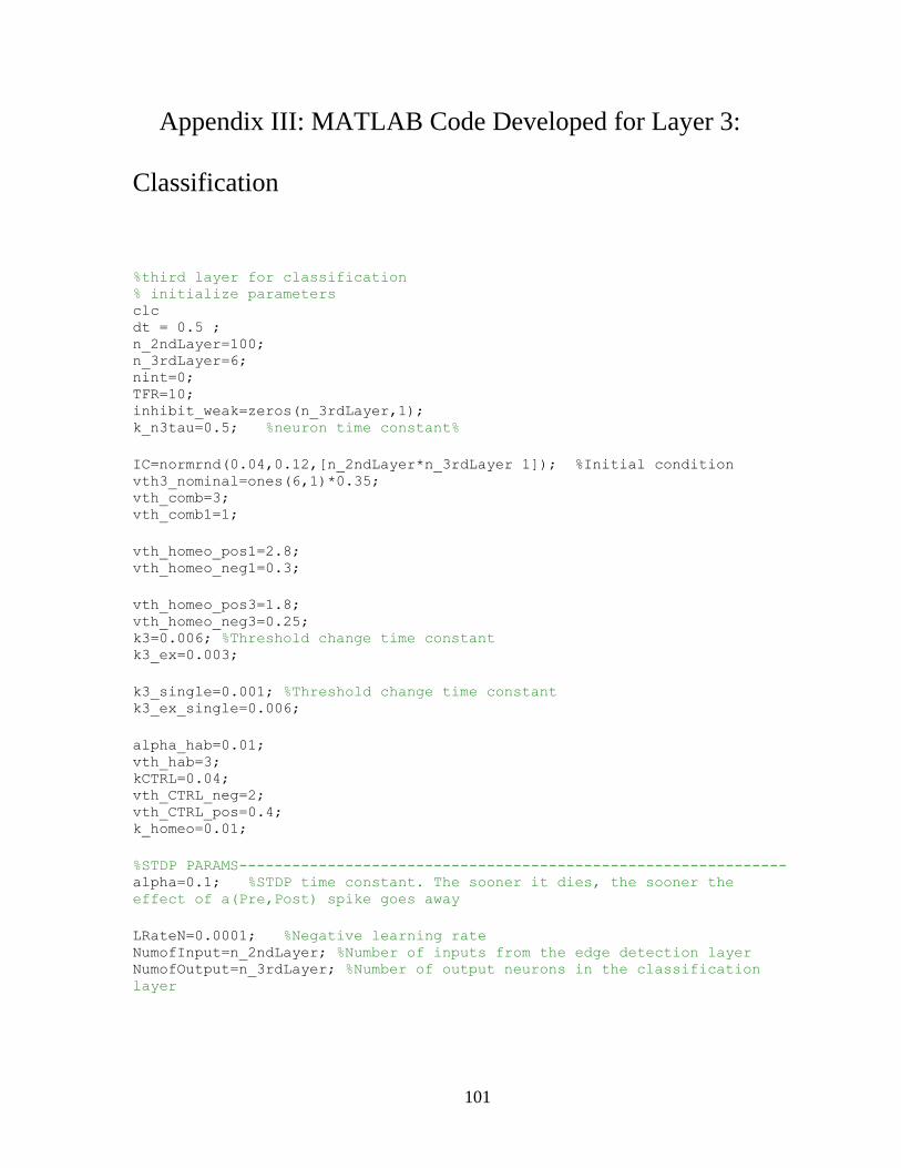
101
Appendix III: MATLAB Code Developed for Layer 3:
Classification
%third layer for classification % initialize parameters clc dt = 0.5 ; n_2ndLayer=100; n_3rdLayer=6; nint=0; TFR=10; inhibit_weak=zeros(n_3rdLayer,1); k_n3tau=0.5; %neuron time constant%
IC=normrnd(0.04,0.12,[n_2ndLayer*n_3rdLayer 1]); %Initial condition vth3_nominal=ones(6,1)*0.35; vth_comb=3; vth_comb1=1;
vth_homeo_pos1=2.8; vth_homeo_neg1=0.3;
vth_homeo_pos3=1.8; vth_homeo_neg3=0.25; k3=0.006; %Threshold change time constant k3_ex=0.003;
k3_single=0.001; %Threshold change time constant k3_ex_single=0.006;
alpha_hab=0.01; vth_hab=3; kCTRL=0.04; vth_CTRL_neg=2; vth_CTRL_pos=0.4; k_homeo=0.01;
%STDP PARAMS-------------------------------------------------------------- alpha=0.1; %STDP time constant. The sooner it dies, the sooner the
effect of a(Pre,Post) spike goes away
LRateN=0.0001; %Negative learning rate NumofInput=n_2ndLayer; %Number of inputs from the edge detection layer NumofOutput=n_3rdLayer; %Number of output neurons in the classification
layer
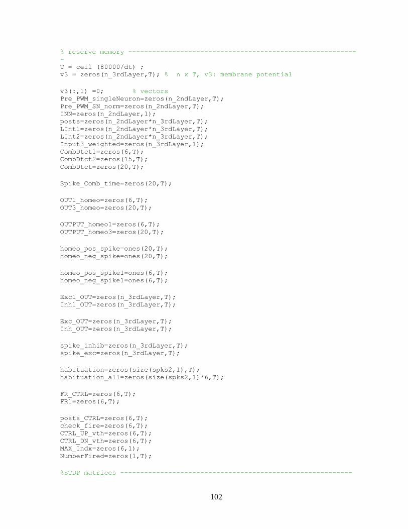
102
% reserve memory ---------------------------------------------------------
- T = ceil (80000/dt) ; v3 = zeros(n_3rdLayer,T); % n x T, v3: membrane potential
v3(:,1) =0; % vectors Pre_PWM_singleNeuron=zeros(n_2ndLayer,T); Pre_PWM_SN_norm=zeros(n_2ndLayer,T); INN=zeros(n_2ndLayer,1); posts=zeros(n_2ndLayer*n_3rdLayer,T); LInt1=zeros(n_2ndLayer*n_3rdLayer,T); LInt2=zeros(n_2ndLayer*n_3rdLayer,T); Input3_weighted=zeros(n_3rdLayer,1); CombDtct1=zeros(6,T); CombDtct2=zeros(15,T); CombDtct=zeros(20,T);
Spike_Comb_time=zeros(20,T);
OUT1_homeo=zeros(6,T); OUT3_homeo=zeros(20,T);
OUTPUT_homeo1=zeros(6,T); OUTPUT_homeo3=zeros(20,T);
homeo_pos_spike=ones(20,T); homeo_neg_spike=ones(20,T);
homeo_pos_spike1=ones(6,T); homeo_neg_spike1=ones(6,T);
Exc1_OUT=zeros(n_3rdLayer,T); Inh1_OUT=zeros(n_3rdLayer,T);
Exc_OUT=zeros(n_3rdLayer,T); Inh_OUT=zeros(n_3rdLayer,T);
spike_inhib=zeros(n_3rdLayer,T); spike_exc=zeros(n_3rdLayer,T);
habituation=zeros(size(spks2,1),T); habituation_all=zeros(size(spks2,1)*6,T);
FR_CTRL=zeros(6,T); FR1=zeros(6,T);
posts_CTRL=zeros(6,T); check_fire=zeros(6,T); CTRL_UP_vth=zeros(6,T); CTRL_DN_vth=zeros(6,T); MAX_Indx=zeros(6,1); NumberFired=zeros(1,T);
%STDP matrices ----------------------------------------------------------

103
Pre=zeros(n_2ndLayer*n_3rdLayer,T); Pre_PWM=zeros(n_2ndLayer*n_3rdLayer,T); Pre_PWM_norm=zeros(n_2ndLayer*n_3rdLayer,T); Post_PWM=zeros(n_2ndLayer*n_3rdLayer,T); dwP=zeros(NumofInput*NumofOutput,T); dwN=zeros(NumofInput*NumofOutput,T); dw=zeros(NumofInput*NumofOutput,T); w=zeros(NumofInput*NumofOutput,T); y1_STDP=zeros(NumofInput*NumofOutput,T); y2_STDP=zeros(NumofInput*NumofOutput,T); tint=20; vth_time=zeros(6,T);
vth3=vth3_nominal; % for loop over time------------- for t =1:T-1; %LRateN=0.0002*exp(-0.000025*t); %Negative learning rate LRateP=0.0072*exp(-0.00003*t); %Positive learning rate % Reseting values at the frame rate clock cycle
if floor(t*dt/TFR)==t*dt/TFR tint=t; nint=floor(t*dt/TFR); v3(:,t)=0; % reset membrane potential Pre_PWM_singleNeuron(:,t)=0; % Reset the input Pre_PWM_SN_norm(:,t)=0; inhibit_strong=0; % Reset inhibit signal inhibit_weak=0; Pre_PWM(:,t)=0; % Reset the SR latch with the Pre connected
to it Post_PWM(:,t)=0; % Reset the SR latch with the Post connected
to it Pre_PWM_norm(:,t)=0; y1_STDP(:,t)=0; y2_STDP(:,t)=0; LInt1(:,t)=0; LInt2(:,t)=0; dwP(:,t)=0; dwN(:,t)=0; CombDtct(:,t)=0; CombDtct2(:,t)=0; NumberFired(t-1)=0; MAX_Indx=zeros(6,1); end
w(:,1)=IC; Pre_PWM_singleNeuron(:,t+1)=Pre_PWM_singleNeuron(:,t)+spks2(:,t+1);
%If there is an spike in the time frame, keep it until the end of the time
window.
Pre_PWM(:,t)=[Pre_PWM_singleNeuron(:,t);Pre_PWM_singleNeuron(:,t);Pre_PWM_
singleNeuron(:,t);Pre_PWM_singleNeuron(:,t);Pre_PWM_singleNeuron(:,t);Pre_
PWM_singleNeuron(:,t)]; %NEW
Pre(:,t)=[spks2(:,t);spks2(:,t);spks2(:,t);spks2(:,t);spks2(:,t);spks2(:,t
)];
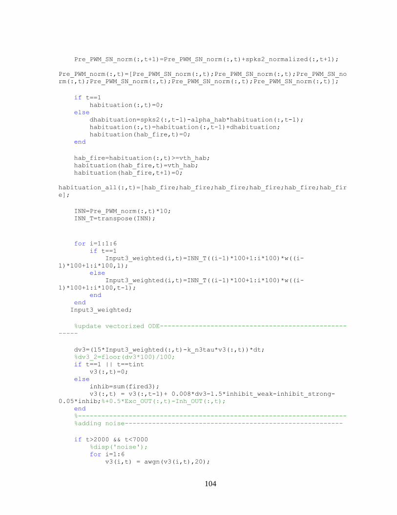
104
Pre_PWM_SN_norm(:,t+1)=Pre_PWM_SN_norm(:,t)+spks2_normalized(:,t+1);
Pre_PWM_norm(:,t)=[Pre_PWM_SN_norm(:,t);Pre_PWM_SN_norm(:,t);Pre_PWM_SN_no
rm(:,t);Pre_PWM_SN_norm(:,t);Pre_PWM_SN_norm(:,t);Pre_PWM_SN_norm(:,t)];
if t==1 habituation(:,t)=0; else dhabituation=spks2(:,t-1)-alpha_hab*habituation(:,t-1); habituation(:,t)=habituation(:,t-1)+dhabituation; habituation(hab_fire,t)=0; end
hab_fire=habituation(:,t)>=vth_hab; habituation(hab_fire,t)=vth_hab; habituation(hab_fire,t+1)=0;
habituation_all(:,t)=[hab_fire;hab_fire;hab_fire;hab_fire;hab_fire;hab_fir
e];
INN=Pre_PWM_norm(:,t)*10; INN_T=transpose(INN);
for i=1:1:6 if t==1 Input3_weighted(i,t)=INN_T((i-1)*100+1:i*100)*w((i-
1)*100+1:i*100,1); else Input3_weighted(i,t)=INN_T((i-1)*100+1:i*100)*w((i-
1)*100+1:i*100,t-1); end end Input3_weighted;
%update vectorized ODE------------------------------------------------
-----
dv3=(15*Input3_weighted(:,t)-k_n3tau*v3(:,t))*dt; %dv3_2=floor(dv3*100)/100; if t==1 || t==tint v3(:,t)=0; else inhib=sum(fired3); v3(:,t) = v3(:,t-1)+ 0.008*dv3-1.5*inhibit_weak-inhibit_strong-
0.05*inhib;%+0.5*Exc_OUT(:,t)-Inh_OUT(:,t); end %--------------------------------------------------------------------- %adding noise--------------------------------------------------------
if t>2000 && t<7000 %disp('noise'); for i=1:6 v3(i,t) = awgn(v3(i,t),20);

105
end end %--------------------------------------------------------------------- %handle spikes ( reset v ) inhibit_weak=zeros(6,1); %take points off only one time. and then let
it be. fired3 = v3(:,t)>= vth3(:,1); % neurons fired? find the ones whose
membrane potential is greater than vth %inhibit_weak=inhibit_weak+sum(fired3); inhibit_weak(fired3)=10; v3(fired3 ,t) = 5; v3(fired3 ,t+1) = 0;
% This part is added because there are multiple neurons firing %bc of the fact that we cannot have small steps of time. Smaller time %steps will cause speed degredation by a lot. So we'll let more
neurons %to fire and then do some compuation to get rid of the ones we dont %want. if t==1 NumberFired(t)=0; else NumberFired(t)=NumberFired(t-1)+sum(fired3); end
if NumberFired(t)>3
SORT_ME=sort(v3(:,t-1),'descend');
if SORT_ME(1)==SORT_ME(2) tt=find(v3(:,t-1)==SORT_ME(1)); MAX_Indx(1)=tt(1); MAX_Indx(2)=tt(2); for j=3:6 MAX_Indx(j)=find(v3(:,t-1)==SORT_ME(j)); end else for j=1:6 MAX_Indx(j)=find(v3(:,t-1)==SORT_ME(j)); end end
if NumberFired(t)==4
for i=0:2:4 if sum(fired3)-NumberFired(t-1)==i fired3(MAX_Indx(i/2+2))=0; v3(MAX_Indx(i/2+2),t)=0;
end NumberFired(t)=0; end elseif NumberFired(t)==5 for i=1:2:5 if sum(fired3)-NumberFired(t-1)==i

106
fired3(MAX_Indx(i/2+3/2:i/2+5/2))=0; v3(MAX_Indx(i/2+3/2:i/2+5/2),t)=0; end NumberFired(t)=0; end elseif NumberFired(t)==6 for i=2:2:6 if sum(fired3)-NumberFired(t-1)==i fired3(MAX_Indx(i/2+1:i/2+3))=0; v3(MAX_Indx(i/2+1:i/2+3))=0; end end NumberFired(t)=0; end
end
%CONTROL THE FIRING RATE ---------------------------------------------
-
posts_CTRL(:,t)=fired3; if t==1 FR_CTRL(:,t)=0.75; else dFR1=posts_CTRL(:,t-1)-kCTRL*FR_CTRL(:,t-1); FR1(:,t)=FR1(:,t-1)+dFR1; FR_CTRL(:,t)=0.75+FR1(:,t); end FR_fire_neg=FR_CTRL(:,t)>=vth_CTRL_neg; FR_fire_pos=FR_CTRL(:,t)<=vth_CTRL_pos;
FR_CTRL(FR_fire_neg,t)=vth_CTRL_neg; FR_CTRL(FR_fire_pos,t)=vth_CTRL_pos;
FR1(FR_fire_neg,t)=0; FR1(FR_fire_pos,t)=0;
check_fire(:,t)=FR_fire_pos; %-------------------------------------------------------------------- %NEURAL STATE MACHINE------------------------------------------------
Index=1; dCombDtct=zeros(NumofOutput,1); dCombDtct2=zeros(NumofOutput,1); dCombDtct1=zeros(NumofOutput,1);
%combinations of 1----------------- combMAT1=nchoosek(1:NumofOutput,1);
for m=1:size(combMAT1,1) if t==1 || t==tint dCombDtct1(m)=0; else dCombDtct1(m)=(sum(fired3(combMAT1(m,:)))); end
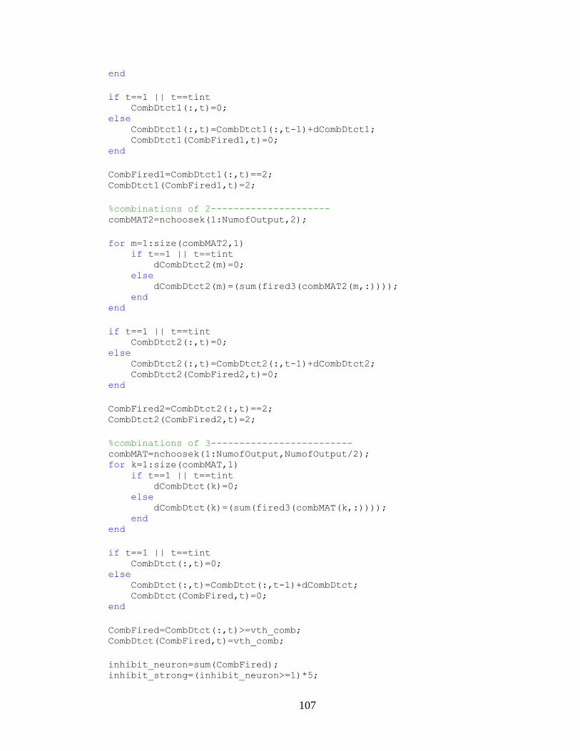
107
end
if t==1 || t==tint CombDtct1(:,t)=0; else CombDtct1(:,t)=CombDtct1(:,t-1)+dCombDtct1; CombDtct1(CombFired1,t)=0; end
CombFired1=CombDtct1(:,t)==2; CombDtct1(CombFired1,t)=2;
%combinations of 2--------------------- combMAT2=nchoosek(1:NumofOutput,2);
for m=1:size(combMAT2,1) if t==1 || t==tint dCombDtct2(m)=0; else dCombDtct2(m)=(sum(fired3(combMAT2(m,:)))); end end
if t==1 || t==tint CombDtct2(:,t)=0; else CombDtct2(:,t)=CombDtct2(:,t-1)+dCombDtct2; CombDtct2(CombFired2,t)=0; end
CombFired2=CombDtct2(:,t)==2; CombDtct2(CombFired2,t)=2;
%combinations of 3------------------------- combMAT=nchoosek(1:NumofOutput,NumofOutput/2); for k=1:size(combMAT,1) if t==1 || t==tint dCombDtct(k)=0; else dCombDtct(k)=(sum(fired3(combMAT(k,:)))); end end
if t==1 || t==tint CombDtct(:,t)=0; else CombDtct(:,t)=CombDtct(:,t-1)+dCombDtct; CombDtct(CombFired,t)=0; end
CombFired=CombDtct(:,t)>=vth_comb; CombDtct(CombFired,t)=vth_comb;
inhibit_neuron=sum(CombFired); inhibit_strong=(inhibit_neuron>=1)*5;

108
spk_comb=double(CombDtct(:,t)==vth_comb); spk_comb1=double(CombDtct1(:,t)==vth_comb1);
%-------------------------------------------------------------------- % Homeostatis SINGLE-------------------------------------------------
if t==1 OUTPUT_homeo1(:,t)=0.75; fired_homeo_pos1=1; fired_homeo_neg1=1; homeo_pos_spike1(:,t)=0; homeo_neg_spike1(:,t)=0; else
dOUT1=(spk_comb1-k_homeo*OUTPUT_homeo1(:,t-1))*dt; OUT1_homeo(:,t)=OUT1_homeo(:,t-1)+1*dOUT1; OUT1_homeo(fired_homeo_pos1,t)=0; %to reset the value after firing OUT1_homeo(fired_homeo_neg1,t)=0; %to reset the value after firing OUTPUT_homeo1(:,t)=OUT1_homeo(:,t)+0.75; OUTPUT_homeo1(:,1)=0.75; fired_homeo_pos1=OUTPUT_homeo1(:,t)>=vth_homeo_pos1; fired_homeo_neg1=OUTPUT_homeo1(:,t)<=vth_homeo_neg1;
OUTPUT_homeo1(fired_homeo_pos1,t)=vth_homeo_pos1; OUTPUT_homeo1(fired_homeo_neg1,t)=vth_homeo_neg1;
homeo_pos_spike1(:,t)=fired_homeo_pos1; homeo_neg_spike1(:,t)=fired_homeo_neg1;
end
if t==1 Exc1_OUT(:,1)=0; Inh1_OUT(:,1)=0; else %Excitatory Input to the output neuron OR INSTEAD WE CHANGE THE %THRESHOLD dExc1_OUT=(homeo_neg_spike1(:,t-1)-k3_ex_single*Exc1_OUT(:,t-
1))*dt; Exc1_OUT(:,t)=Exc1_OUT(:,t-1)+dExc1_OUT;
%Inhibitory Input to the output neuron OR INSTEAD WE CHANGE THE %THRESHOLD
dInh_OUT1=(homeo_pos_spike1(:,t-1)-k3_single*Inh1_OUT(:,t-1))*dt; Inh1_OUT(:,t)=Inh1_OUT(:,t-1)+dInh_OUT1; if Exc1_OUT(:,t)<=0 Exc1_OUT(:,t)=0; end
if Inh1_OUT(:,t)<=0 Inh1_OUT(:,t)=0; end

109
end %------------------------------------------------------------------- %Homeostasis TRIPLE-------------------------------------------------
if t==1 OUTPUT_homeo3(:,t)=0.75; fired_homeo_pos3=1; fired_homeo_neg3=1; homeo_pos_spike(:,t)=0; homeo_neg_spike(:,t)=0; else Spike_Comb_time(:,t)=spk_comb; dOUT3=(spk_comb-k_homeo*OUTPUT_homeo3(:,t-1))*dt; OUT3_homeo(:,t)=OUT3_homeo(:,t-1)+1*dOUT3; OUT3_homeo(fired_homeo_pos3,t)=0; %to reset the value after firing OUT3_homeo(fired_homeo_neg3,t)=0; %to reset the value after firing OUTPUT_homeo3(:,t)=OUT3_homeo(:,t)+0.75; OUTPUT_homeo3(:,1)=0.75; fired_homeo_pos3=OUTPUT_homeo3(:,t)>=vth_homeo_pos3; fired_homeo_neg3=OUTPUT_homeo3(:,t)<=vth_homeo_neg3;
OUTPUT_homeo3(fired_homeo_pos3,t)=vth_homeo_pos3; OUTPUT_homeo3(fired_homeo_neg3,t)=vth_homeo_neg3;
homeo_pos_spike(:,t)=fired_homeo_pos3; homeo_neg_spike(:,t)=fired_homeo_neg3;
end
for i=1:NumofOutput FindIndx=find(combMAT==i); GR20=find(20<FindIndx & FindIndx<=40); GR40=find(FindIndx>40); FindIndx(GR20)=FindIndx(GR20)-20; FindIndx(GR40)=FindIndx(GR40)-40; spike_inhib(i,t)=sum(homeo_pos_spike(FindIndx,t)); spike_exc(i,t)=sum(homeo_neg_spike(FindIndx,t)); end
if t==1 Exc_OUT(:,1)=0; Inh_OUT(:,1)=0; else
%Excitatory Input to the output neuron OR INSTEAD WE CHANGE THE %THRESHOLD
dExc_OUT=(spike_exc(:,t-1)-k3_ex*Exc_OUT(:,t-1))*dt; Exc_OUT(:,t)=Exc_OUT(:,t-1)+dExc_OUT;
%Inhibitory Input to the output neuron OR INSTEAD WE CHANGE THE
110
%THRESHOLD
dInh_OUT=(spike_inhib(:,t-1)-k3*Inh_OUT(:,t-1))*dt; Inh_OUT(:,t)=Inh_OUT(:,t-1)+dInh_OUT; if Exc_OUT(:,t)<=0 Exc_OUT(:,t)=0; end
if Inh_OUT(:,t)<=0 Inh_OUT(:,t)=0; end end
if t==1 CTRL_UP_vth(:,t)=0; CTRL_DN_vth(:,t)=0; else CTRL_UP_vth(:,t)=CTRL_UP_vth(:,t-1)+FR_fire_neg; CTRL_DN_vth(:,t)=CTRL_DN_vth(:,t-1)+FR_fire_pos; end
%vth3(:,1)=vth3_nominal+0.025*Inh_OUT(:,t)-
0.011*Exc_OUT(:,t)+0.025*Inh1_OUT(:,t)-0.011*Exc1_OUT(:,t); vth3(:,1)=vth3_nominal+0.025*Inh_OUT(:,t)-
0.01*Exc_OUT(:,t);%+0.011*Inh1_OUT(:,t)-0.011*Exc1_OUT(:,t);
for i=1:7 if t>2*(i*15400-1400) && t<2*(i*15400) vth3(:,1)=vth_time(:,i*15400-1400); end end
vth_time(:,t)=vth3;
%END OF HOMEOSTASIS---------------------------------------------------
-
% WEIGHT UPDATE-------------------------------------------------------
- %SR latch output
%POSITIVE WEIGHT CHANGE-----------------------------------------------
-
%decay in time dLInt1=(Pre(:,t)-alpha*LInt1(:,t))*dt; LInt1(:,t+1)=LInt1(:,t)+dLInt1;
% SR-leaky integrator (SR minus decay)
y1_STDP(:,t)=Pre_PWM(:,t)-LInt1(:,t); %y1_STDP(:,t)=LInt1(:,t);
for j=1:6

111
posts((j-1)*100+1:j*100,t)=fired3(j); end
dwP(:,t)=posts(:,t).*y1_STDP(:,t)*LRateP; Post_PWM(:,t+1)=Post_PWM(:,t)+posts(:,t);
%NEGATIVE WEIGHT CHANGE-----------------------------------------------
%decay in time dOUT2=(posts(:,t)-alpha*LInt2(:,t))*dt; LInt2(:,t+1)=LInt2(:,t)+dOUT2; y2_STDP(:,t)=Post_PWM(:,t)-alpha*LInt2(:,t);
% SR-decay
dwN(:,t)=Pre(:,t).*y2_STDP(:,t)*LRateN+~Pre_PWM(:,t).*posts(:,t)*LRateN; dw(:,t)=0.3*(dwP(:,t)-dwN(:,t))-0.0081*exp(-
0.00003*t)*habituation_all(:,t); if t==1 w(:,t)=IC; else w(:,t)=w(:,t-1)+dw(:,t); end for i=1:n_2ndLayer*n_3rdLayer if w(i,t)>=0.7 w(i,t)=0.7; elseif w(i,t)<=-0.01 w(i,t)=-0.01; end end %------------------------------------------------------------------------- end %Plot Pre spikes %figure(1) %plot (X_2(idx_2),Y3_2(idx_2) ,['r','.'] ) ; %xlim([0,T*dt]); %ylim([0,n_2ndLayer]);
%Plot spike raster figure(2) spks3 = double(v3==5); clf , hold on ; [X_3,Y3_3] = meshgrid((0:T-1)*dt,1:n_3rdLayer) ; idx_3 = find(spks3==1) ; plot (X_3(idx_3),Y3_3(idx_3) ,['r','.'] ) ; xlim([0,T*dt]); ylim([0,n_3rdLayer]); xlabel('Time[ms]') ylabel('Unit #')
%plot weights------------------------------------------------------------- %for i=1:6 % figure(i+2) % plot((0:T-1)*dt,w((i-1)*100+1:i*100,:));

112
%end
%plot homeostatic spikes ------------------------------------------------ %figure(10) %clf , hold on ; %[X_neg_homeo,Y_neg_homeo] = meshgrid((0:T-1)*dt,1:20) ; %idx_homeo_neg = find(homeo_neg_spike==1) ; %plot(X_neg_homeo(idx_homeo_neg),Y_neg_homeo(idx_homeo_neg),['r','.']); %xlim([0,T*dt]); %ylim([0,n_3rdLayer]); %xlabel('Time[ms]') %ylabel('Unit #')