university of groningen surface wave control for large ... · a. m. baryshev and w. jellema are...
TRANSCRIPT
University of Groningen
Surface Wave Control for Large Arrays of Microwave Kinetic Inductance DetectorsYates, Stephen J. C.; Barychev, Andrei; Yurduseven, Ozan; Bueno, Juan; Davis, Kristina K.;Ferrari, Lorenza; Jellema, Willem; Llombart, Nuria; Murugesan, Vignesh; Thoen, David J.Published in:Ieee transactions on terahertz science and technology
DOI:10.1109/TTHZ.2017.2755500
IMPORTANT NOTE: You are advised to consult the publisher's version (publisher's PDF) if you wish to cite fromit. Please check the document version below.
Document VersionPublisher's PDF, also known as Version of record
Publication date:2017
Link to publication in University of Groningen/UMCG research database
Citation for published version (APA):Yates, S. J. C., Baryshev, A. M., Yurduseven, O., Bueno, J., Davis, K. K., Ferrari, L., ... Baselmans, J. J. A.(2017). Surface Wave Control for Large Arrays of Microwave Kinetic Inductance Detectors. Ieeetransactions on terahertz science and technology, 7(6), 789-799. DOI: 10.1109/TTHZ.2017.2755500
CopyrightOther than for strictly personal use, it is not permitted to download or to forward/distribute the text or part of it without the consent of theauthor(s) and/or copyright holder(s), unless the work is under an open content license (like Creative Commons).
Take-down policyIf you believe that this document breaches copyright please contact us providing details, and we will remove access to the work immediatelyand investigate your claim.
Downloaded from the University of Groningen/UMCG research database (Pure): http://www.rug.nl/research/portal. For technical reasons thenumber of authors shown on this cover page is limited to 10 maximum.
Download date: 11-02-2018

IEEE TRANSACTIONS ON TERAHERTZ SCIENCE AND TECHNOLOGY, VOL. 7, NO. 6, NOVEMBER 2017 789
Surface Wave Control for Large Arrays of MicrowaveKinetic Inductance Detectors
Stephen J. C. Yates , Andrey M. Baryshev, Ozan Yurduseven , Student Member, IEEE, Juan Bueno,Kristina K. Davis , Lorenza Ferrari , Willem Jellema, Nuria Llombart, Senior Member, IEEE,
Vignesh Murugesan, David J. Thoen , and Jochem J. A. Baselmans
Abstract—Large ultrasensitive detector arrays are needed forpresent and future observatories for far infrared, submillimeterwave (THz), and millimeter wave astronomy. With increasing ar-ray size, it is increasingly important to control stray radiation insidethe detector chips themselves, the surface wave. We demonstratethis effect with focal plane arrays of 880 lens-antenna coupled mi-crowave kinetic inductance detectors (MKIDs). Presented here arenear field measurements of the MKID optical response versus theposition on the array of a reimaged optical source. We demonstratethat the optical response of a detector in these arrays saturates off-pixel at the ∼−30-dB level compared to the peak pixel response.The result is that the power detected from a point source at thepixel position is at a similar level to the stray response integratedover the chip area. With such a contribution, it would be impossibleto measure extended sources, while the point source sensitivity isdegraded due to an increase of the stray loading. However, we showthat by incorporating an on-chip stray light absorber, the surfacewave contribution is reduced by a factor >10. With the on-chipstray light absorber, the point source response is close to simula-tions down to the ∼ −35-dB level, the simulation based on an idealGaussian illumination of the optics. In addition, as a crosscheck,we show that the extended source response of a single pixel in the
Manuscript received April 12, 2017; revised July 7, 2017; accepted September7, 2017. Date of publication November 1, 2017; date of current version Novem-ber 8, 2017. This work was supported in part by the European Reseach Council(ERC) under ERC Starting Grant ERC-2009-StG Grant 240602 TFPA and inpart by a collaborative project, SPACEKIDs, funded via Grant 313320 providedby the European Commission under Theme SPA.2012.2.2-01 of FrameworkProgramme 7. The work of N. Llombart was supported by the ERC StartingGrant LAA-THz-CC (639749). This work of J. J. A. Baselmans was supportedby the ERC consolidator Grant COG 648135 MOSAIC. (Corresponding author:Stephen J. C. Yates.)
S. J. C. Yates and L. Ferrari are with SRON, 9747 AD Groningen. The Nether-lands (e-mail: [email protected]; [email protected]).
A. M. Baryshev and W. Jellema are with SRON, 9747 AD Groningen,The Netherlands, and also with the the Kapteyn Astronomical Institute,University of Groningen, 9700 AV Groningen, The Netherlands (e-mail:[email protected]; [email protected]).
O. Yurduseven, N. Llombart, and D. J. Thoen are with the Terahertz Sens-ing Group, Faculty of Electrical Engineering, Mathematics and Computer Sci-ence, Delft University of Technology, 2628 CD Delft, The Netherlands (e-mail:[email protected]; [email protected]; [email protected]).
J. Bueno and V. Murugesan are with SRON, 3584 CA Utrecht, The Nether-lands (e-mail: [email protected]; [email protected]).
K. K. Davis is with the School of Earth and Space Exploration, Arizona StateUniversity, Tempe, AZ 85281 USA (e-mail: [email protected]).
J. J. A. Baselmans is with SRON, 3584 CA Utrecht, The Netherlands, andalso with the Terahertz Sensing Group, Faculty of Electrical Engineering, Math-ematics and Computer Science, Delft University of Technology, 2628 CD Delft,The Netherlands (e-mail: [email protected]).
Color versions of one or more of the figures in this paper are available onlineat http://ieeexplore.ieee.org.
Digital Object Identifier 10.1109/TTHZ.2017.2755500
array with the absorbing grid is in agreement with the integral ofthe point source measurements.
Index Terms—Antenna, kinetic inductance detector (KID),low-temperature detector, microwave kinetic inductance detector(MKID), surface wave, submillimeter wave, terahertz, twinslot.
I. INTRODUCTION
P resent and future observatories for far infrared (FIR,∼1–10 THz), submillimeter wave (0.3–1 THz), and mil-
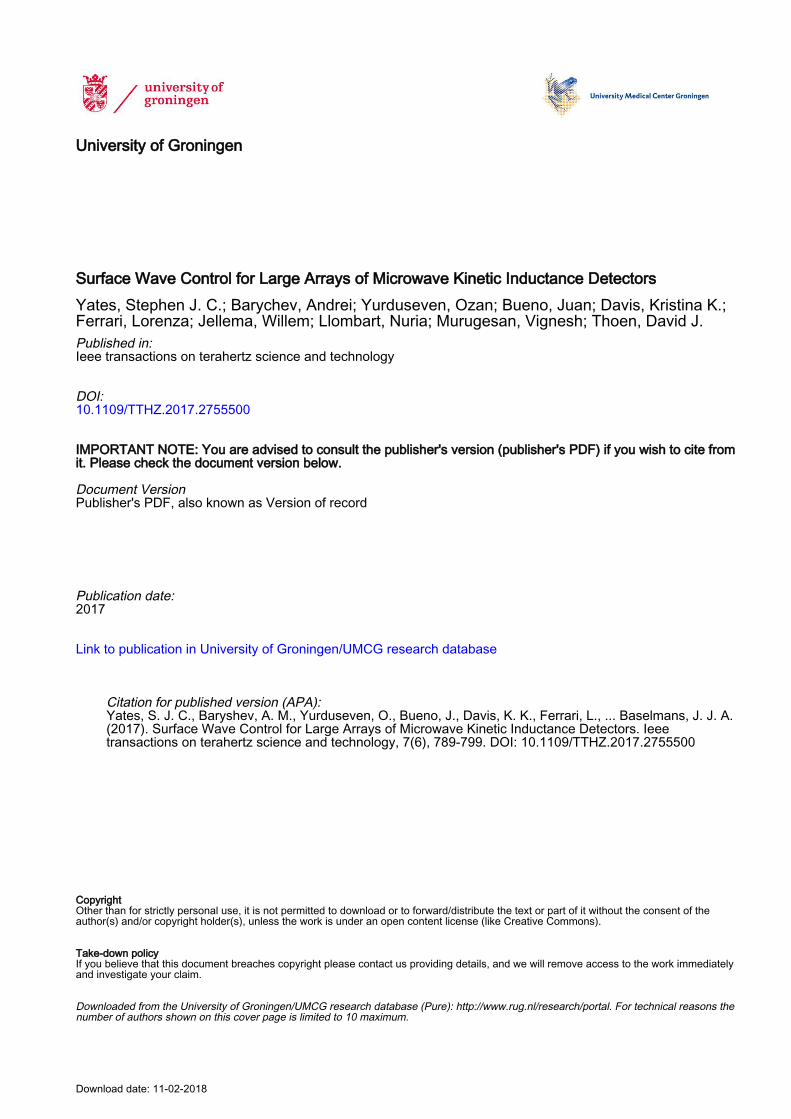
limeter wave (50–300 GHz) astronomy need increasingly largearrays of ultrasensitive power (“direct”) detectors [1]. This re-quires a CCD-like approach in which large-scale monolithicdetector chips are combined with a multiplexed readout. Cur-rent imaging arrays for the FIR and the submillimeter regimeare based upon transition edge sensors [2] or microwave kineticinductance detectors (MKIDs) [3]. In both cases, the detectorarrays are based upon large, monolithic chips, where radiationcoupling is achieved using planar absorbers, lenses, or horns.With ever increasing array size, it becomes critically importantto control stray radiation inside these detector chips. Even inthe best cases, the radiation absorption in a single pixel is notperfect: Part of the radiation can be reflected and rescatteredinto the dielectric of the detector chip. This confined radiationis commonly referred to as a surface wave. Typical chip ma-terials such as Si have a high refractive index, increasing theprobability of total internal reflection. To illustrate the effect,we show in Fig. 1(a) the spatial response of a central pixel of an880 pixel array of lens-antenna-coupled MKIDs as a functionof the position of a small calibration source in the image planeof the chip, the system beam pattern. We observe a localizedpeak response, the main beam, at the pixel position. However,we also observe a low level of response over the entire chip area,which we will refer to as the pedestal response in the remainderof the text. The pedestal response consists of power coupledto the chip at a position spatially far away from the measuredpixel: It is detected at the pixel under test due to scattering ofradiation inside the detector chip. Normalizing the system beampattern to its maximum response, the pedestal response is seenat a level of∼−30 dB. In this particular case, the total integratedstray power in the pedestal at −30 dB is similar to the power inthe main beam. This will render imaging of extended sourcesimpossible and results in excess power loading when using thisarray for ground based astronomy. In this paper, we study thisproblem in detail by comparing two large imaging arrays, which
2156-342X © 2017 IEEE. Translations and content mining are permitted for academic research only. Personal use is also permitted, but republication/redistributionrequires IEEE permission. See http://www.ieee.org/publications standards/publications/rights/index.html for more information.
790 IEEE TRANSACTIONS ON TERAHERTZ SCIENCE AND TECHNOLOGY, VOL. 7, NO. 6, NOVEMBER 2017
Fig. 1. Position dependent response in decibel of one pixel to a point sourceplaced in a reimaged focal plane with a magnification of 3. The −3-dB and−27-dB contours are shown. The circles show the fitted 3-dB beams of allfound pixels, shown to show the extent of the array. Two arrays are shown: (a)without on-chip stray light absorbing mesh; (b) with absorbing mesh. Note thelarge area response at the ∼ −30-dB level without the mesh disappears on thearray with the on-chip absorbing mesh.
are based upon lens-antenna-coupled MKIDs. Both arrays areidentical with the exception of an absorbing mesh layer designedto absorb rescattered radiation propagating through the detec-tor chip, with the resultant pedestal-suppressed spatial responseshown in Fig. 1(b). We discuss in detail the design, fabrication,and testing of these two systems and demonstrate that the afore-mentioned problem can be reduced very significantly by usinga stray-light absorbing layer.
II. ARRAY DESIGN
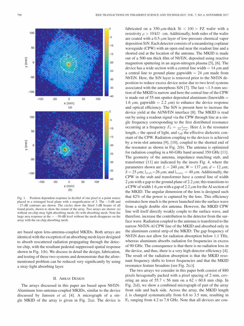
The arrays discussed in this paper are based upon NbTiN-Aluminum lens-antenna-coupled MKIDs, similar to the devicediscussed by Janssen et al. [4]. A micrograph of a sin-gle MKID of the array is given in Fig. 2(a). The device is
fabricated on a 350-μm-thick Si < 100 > FZ wafer with aresistivity ρ > 10 kΩ · cm. Additionally, both sides of the waferare coated with a 0.5-μm layer of low-pressure chemical vapordeposition SiN. Each detector consists of a meandering coplanarwaveguide (CPW) with an open end near the readout line and ashorted end at the location of the antenna. The MKID is madeout of a 500-nm thick film of NbTiN, deposited using reactivemagnetron sputtering in an argon-nitrogen plasma [5], [6]. Thedevice has a wide section with a central line width = 14 μm anda central line to ground plane gapwidth = 24 μm made fromNbTiN. Here, the SiN layer is removed prior to the NbTiN de-position to reduce excess device noise due to two level systemsassociated with the amorphous SiN [7]. The last ∼1.5-mm sec-tion of the MKID is narrow and here the central line of the CPWis made out of 55-nm sputter deposited aluminum (linewidth =1.6 μm, gapwidth = 2.2 μm) to enhance the device responseand optical efficiency. The SiN is present here to increase thedevice yield at the Al/NbTiN interface [8]. The MKID is readout by using a readout signal via the CPW through line at a sin-gle frequency corresponding to the first distributed resonanceoccurring at a frequency F0 = c
4L√
εeff. Here L is the resonator
length, c the speed of light, and εeff the effective dielectric con-stant of the CPW. Radiation coupling to the devices is achievedby a twin-slot antenna [9], [10], coupled to the shorted end ofthe resonator as shown in Fig. 2(b). The antenna is optimizedfor radiation coupling in a 60-GHz band around 350 GHz [11].The geometry of the antenna, impedance matching stub, andtransformer [11] are indicated by the insets Fig. 4, where theparameters shown are: L = 240 μm; W = 137 μm; d = 12 μm;S = 25 μm; lstub=26 μm; and ltrans = 40 μm. Additionally, theCPW in the stub and transformer have a central line of width2 μm with a gap to the ground plane of 2.2 μm; this transitions toa CPW of width 1.6 μm with a gap of 2.2 μm for the Al section ofthe MKID. The angular dimension of the lens is designed suchthat 82% of the power is captured by the lens. This efficiencyestimates how much is the power launched into the surface wavefrom a single double slot antenna. However, the MKID CPWline will itself directly weakly couple to the surface wave, andtherefore, increase the contribution to the detector from the sur-face wave. Radiation coupled to the antenna is transferred to thenarrow NbTiN-Al CPW line of the MKID and absorbed only inthe aluminum central strip of the MKID: The gap frequency ofNbTiN does not allow for radiation absorption below 1.1 THz,whereas aluminum absorbs radiation for frequencies in excessof 90 GHz. The consequence is that there is no radiation loss inthe device, and thus, there is a very high detector efficiency [4].The result of the radiation absorption is that the MKID reso-nant frequency shifts to lower frequencies and that the MKIDresonance feature broadens [see Fig. 2(c)].
The two arrays we consider in this paper both consist of 880pixels hexagonally packed with a pixel spacing of 2 mm, cov-ering an area of 55.7 × 56 mm on a 62 × 60.8 mm chip. InFig. 2(d), we show a combined micrograph of part of the arrayfront side and back side. Across the array, the MKID lengthL is changed systematically from 6.6 to 3.5 mm, resulting inF0 ranging from 4.2 to 7.8 GHz. Note that all devices are cou-
YATES et al.: SURFACE WAVE CONTROL FOR LARGE ARRAYS OF MKIDs 791
Fig. 2. (a) Optical micrograph of a single pixel of the array, artificial coloring is used to highlight the different metals. (b) Zoom in to the antenna structure ofpanel (a). (c) Transmission of the readout line around a single MKID, measured at two different values of the power absorbed by the device, showing the responsemechanism of the MKID. (d) Optical micrograph of the array, with the front side (top) and backside (bottom) showing the detectors on the front side and theTa absorbing mesh on the backside, implemented on only one of the two arrays discussed in the text. (e) Assembled detector holder with lens array and SMAconnector for contacting the readout circuitry. The top panel shows schematically the assembled cross section.
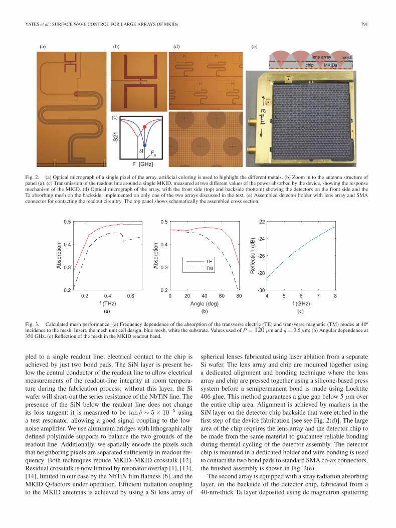
Fig. 3. Calculated mesh performance: (a) Frequency dependence of the absorption of the transverse electric (TE) and transverse magnetic (TM) modes at 40ºincidence to the mesh. Insert, the mesh unit cell design, blue mesh, white the substrate. Values used of P = 120 μm and g = 3.5 μm; (b) Angular dependence at350 GHz. (c) Reflection of the mesh in the MKID readout band.
pled to a single readout line; electrical contact to the chip isachieved by just two bond pads. The SiN layer is present be-low the central conductor of the readout line to allow electricalmeasurements of the readout-line integrity at room tempera-ture during the fabrication process; without this layer, the Siwafer will short-out the series resistance of the NbTiN line. Thepresence of the SiN below the readout line does not changeits loss tangent: it is measured to be tan δ ∼ 5 × 10⁻⁵ usinga test resonator, allowing a good signal coupling to the low-noise amplifier. We use aluminum bridges with lithographicallydefined polyimide supports to balance the two grounds of thereadout line. Additionally, we spatially encode the pixels suchthat neighboring pixels are separated sufficiently in readout fre-quency. Both techniques reduce MKID–MKID crosstalk [12].Residual crosstalk is now limited by resonator overlap [1], [13],[14], limited in our case by the NbTiN film flatness [6], and theMKID Q-factors under operation. Efficient radiation couplingto the MKID antennas is achieved by using a Si lens array of
spherical lenses fabricated using laser ablation from a separateSi wafer. The lens array and chip are mounted together usinga dedicated alignment and bonding technique where the lensarray and chip are pressed together using a silicone-based presssystem before a semipermanent bond is made using Locktite406 glue. This method guarantees a glue gap below 5 μm overthe entire chip area. Alignment is achieved by markers in theSiN layer on the detector chip backside that were etched in thefirst step of the device fabrication [see see Fig. 2(d)]. The largearea of the chip requires the lens array and the detector chip tobe made from the same material to guarantee reliable bondingduring thermal cycling of the detector assembly. The detectorchip is mounted in a dedicated holder and wire bonding is usedto contact the two bond pads to standard SMA co-ax connectors,the finished assembly is shown in Fig. 2(e).
The second array is equipped with a stray radiation absorbinglayer, on the backside of the detector chip, fabricated from a40-nm-thick Ta layer deposited using dc magnetron sputtering
792 IEEE TRANSACTIONS ON TERAHERTZ SCIENCE AND TECHNOLOGY, VOL. 7, NO. 6, NOVEMBER 2017
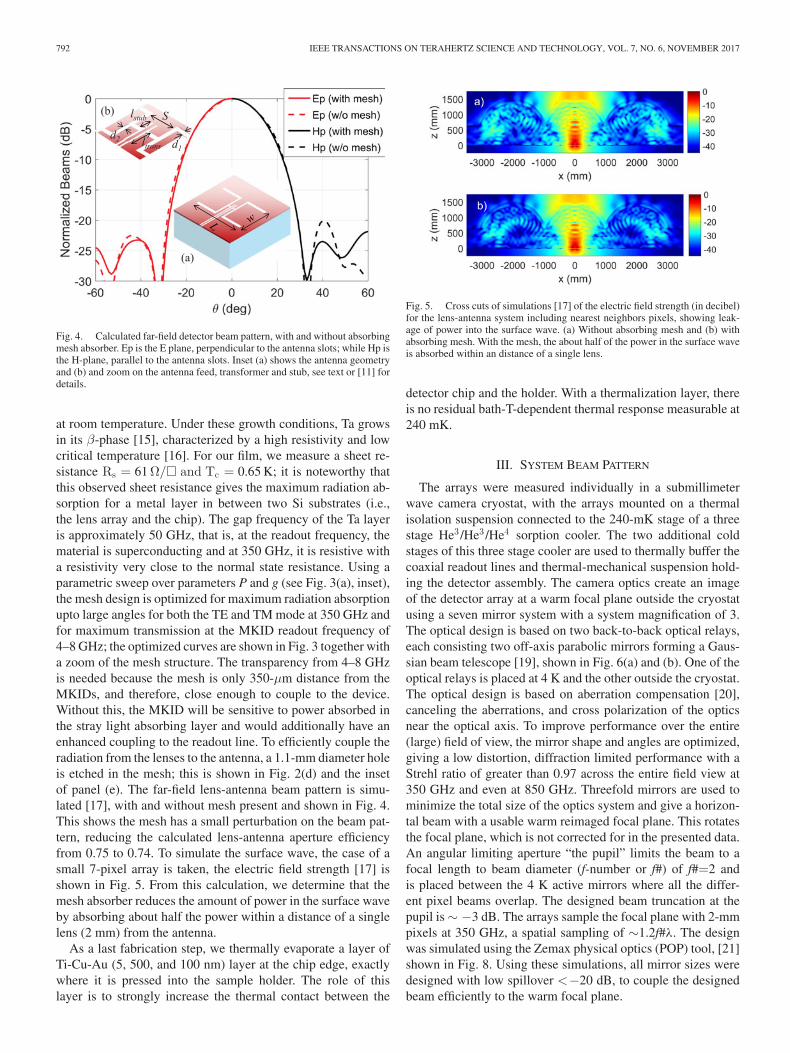
Fig. 4. Calculated far-field detector beam pattern, with and without absorbingmesh absorber. Ep is the E plane, perpendicular to the antenna slots; while Hp isthe H-plane, parallel to the antenna slots. Inset (a) shows the antenna geometryand (b) and zoom on the antenna feed, transformer and stub, see text or [11] fordetails.
at room temperature. Under these growth conditions, Ta growsin its β-phase [15], characterized by a high resistivity and lowcritical temperature [16]. For our film, we measure a sheet re-sistance Rs = 61 Ω/� and Tc = 0.65 K; it is noteworthy thatthis observed sheet resistance gives the maximum radiation ab-sorption for a metal layer in between two Si substrates (i.e.,the lens array and the chip). The gap frequency of the Ta layeris approximately 50 GHz, that is, at the readout frequency, thematerial is superconducting and at 350 GHz, it is resistive witha resistivity very close to the normal state resistance. Using aparametric sweep over parameters P and g (see Fig. 3(a), inset),the mesh design is optimized for maximum radiation absorptionupto large angles for both the TE and TM mode at 350 GHz andfor maximum transmission at the MKID readout frequency of4–8 GHz; the optimized curves are shown in Fig. 3 together witha zoom of the mesh structure. The transparency from 4–8 GHzis needed because the mesh is only 350-μm distance from theMKIDs, and therefore, close enough to couple to the device.Without this, the MKID will be sensitive to power absorbed inthe stray light absorbing layer and would additionally have anenhanced coupling to the readout line. To efficiently couple theradiation from the lenses to the antenna, a 1.1-mm diameter holeis etched in the mesh; this is shown in Fig. 2(d) and the insetof panel (e). The far-field lens-antenna beam pattern is simu-lated [17], with and without mesh present and shown in Fig. 4.This shows the mesh has a small perturbation on the beam pat-tern, reducing the calculated lens-antenna aperture efficiencyfrom 0.75 to 0.74. To simulate the surface wave, the case of asmall 7-pixel array is taken, the electric field strength [17] isshown in Fig. 5. From this calculation, we determine that themesh absorber reduces the amount of power in the surface waveby absorbing about half the power within a distance of a singlelens (2 mm) from the antenna.
As a last fabrication step, we thermally evaporate a layer ofTi-Cu-Au (5, 500, and 100 nm) layer at the chip edge, exactlywhere it is pressed into the sample holder. The role of thislayer is to strongly increase the thermal contact between the
Fig. 5. Cross cuts of simulations [17] of the electric field strength (in decibel)for the lens-antenna system including nearest neighbors pixels, showing leak-age of power into the surface wave. (a) Without absorbing mesh and (b) withabsorbing mesh. With the mesh, the about half of the power in the surface waveis absorbed within an distance of a single lens.
detector chip and the holder. With a thermalization layer, thereis no residual bath-T-dependent thermal response measurable at240 mK.
III. SYSTEM BEAM PATTERN
The arrays were measured individually in a submillimeterwave camera cryostat, with the arrays mounted on a thermalisolation suspension connected to the 240-mK stage of a threestage He3 /He3 /He4 sorption cooler. The two additional coldstages of this three stage cooler are used to thermally buffer thecoaxial readout lines and thermal-mechanical suspension hold-ing the detector assembly. The camera optics create an imageof the detector array at a warm focal plane outside the cryostatusing a seven mirror system with a system magnification of 3.The optical design is based on two back-to-back optical relays,each consisting two off-axis parabolic mirrors forming a Gaus-sian beam telescope [19], shown in Fig. 6(a) and (b). One of theoptical relays is placed at 4 K and the other outside the cryostat.The optical design is based on aberration compensation [20],canceling the aberrations, and cross polarization of the opticsnear the optical axis. To improve performance over the entire(large) field of view, the mirror shape and angles are optimized,giving a low distortion, diffraction limited performance with aStrehl ratio of greater than 0.97 across the entire field view at350 GHz and even at 850 GHz. Threefold mirrors are used tominimize the total size of the optics system and give a horizon-tal beam with a usable warm reimaged focal plane. This rotatesthe focal plane, which is not corrected for in the presented data.An angular limiting aperture “the pupil” limits the beam to afocal length to beam diameter (f-number or f#) of f#=2 andis placed between the 4 K active mirrors where all the differ-ent pixel beams overlap. The designed beam truncation at thepupil is ∼ −3 dB. The arrays sample the focal plane with 2-mmpixels at 350 GHz, a spatial sampling of ∼1.2f#λ. The designwas simulated using the Zemax physical optics (POP) tool, [21]shown in Fig. 8. Using these simulations, all mirror sizes weredesigned with low spillover <−20 dB, to couple the designedbeam efficiently to the warm focal plane.
YATES et al.: SURFACE WAVE CONTROL FOR LARGE ARRAYS OF MKIDs 793
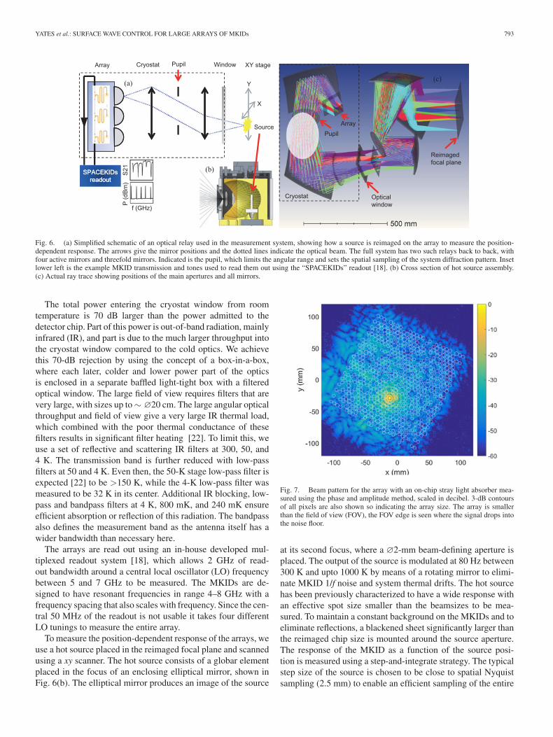
Fig. 6. (a) Simplified schematic of an optical relay used in the measurement system, showing how a source is reimaged on the array to measure the position-dependent response. The arrows give the mirror positions and the dotted lines indicate the optical beam. The full system has two such relays back to back, withfour active mirrors and threefold mirrors. Indicated is the pupil, which limits the angular range and sets the spatial sampling of the system diffraction pattern. Insetlower left is the example MKID transmission and tones used to read them out using the “SPACEKIDs” readout [18]. (b) Cross section of hot source assembly.(c) Actual ray trace showing positions of the main apertures and all mirrors.
The total power entering the cryostat window from roomtemperature is 70 dB larger than the power admitted to thedetector chip. Part of this power is out-of-band radiation, mainlyinfrared (IR), and part is due to the much larger throughput intothe cryostat window compared to the cold optics. We achievethis 70-dB rejection by using the concept of a box-in-a-box,where each later, colder and lower power part of the opticsis enclosed in a separate baffled light-tight box with a filteredoptical window. The large field of view requires filters that arevery large, with sizes up to ∼ ∅20 cm. The large angular opticalthroughput and field of view give a very large IR thermal load,which combined with the poor thermal conductance of thesefilters results in significant filter heating [22]. To limit this, weuse a set of reflective and scattering IR filters at 300, 50, and4 K. The transmission band is further reduced with low-passfilters at 50 and 4 K. Even then, the 50-K stage low-pass filter isexpected [22] to be >150 K, while the 4-K low-pass filter wasmeasured to be 32 K in its center. Additional IR blocking, low-pass and bandpass filters at 4 K, 800 mK, and 240 mK ensureefficient absorption or reflection of this radiation. The bandpassalso defines the measurement band as the antenna itself has awider bandwidth than necessary here.
The arrays are read out using an in-house developed mul-tiplexed readout system [18], which allows 2 GHz of read-out bandwidth around a central local oscillator (LO) frequencybetween 5 and 7 GHz to be measured. The MKIDs are de-signed to have resonant frequencies in range 4–8 GHz with afrequency spacing that also scales with frequency. Since the cen-tral 50 MHz of the readout is not usable it takes four differentLO tunings to measure the entire array.
To measure the position-dependent response of the arrays, weuse a hot source placed in the reimaged focal plane and scannedusing a xy scanner. The hot source consists of a globar elementplaced in the focus of an enclosing elliptical mirror, shown inFig. 6(b). The elliptical mirror produces an image of the source
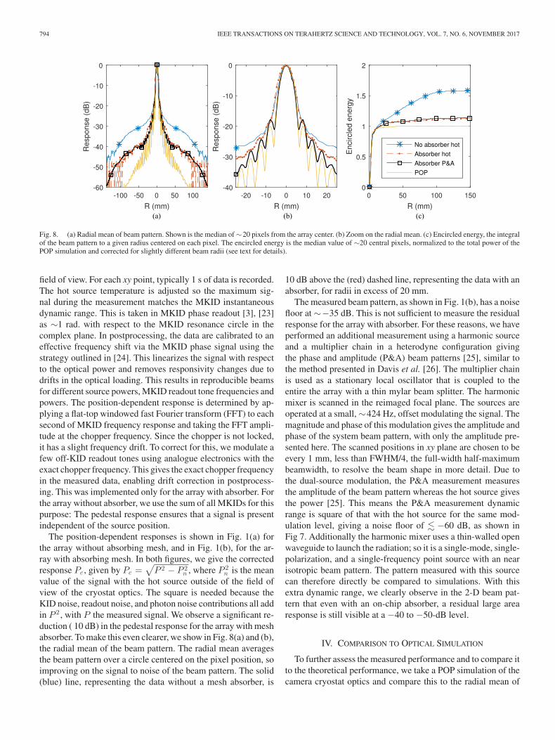
Fig. 7. Beam pattern for the array with an on-chip stray light absorber mea-sured using the phase and amplitude method, scaled in decibel. 3-dB contoursof all pixels are also shown so indicating the array size. The array is smallerthan the field of view (FOV), the FOV edge is seen where the signal drops intothe noise floor.
at its second focus, where a ∅2-mm beam-defining aperture isplaced. The output of the source is modulated at 80 Hz between300 K and upto 1000 K by means of a rotating mirror to elimi-nate MKID 1/f noise and system thermal drifts. The hot sourcehas been previously characterized to have a wide response withan effective spot size smaller than the beamsizes to be mea-sured. To maintain a constant background on the MKIDs and toeliminate reflections, a blackened sheet significantly larger thanthe reimaged chip size is mounted around the source aperture.The response of the MKID as a function of the source posi-tion is measured using a step-and-integrate strategy. The typicalstep size of the source is chosen to be close to spatial Nyquistsampling (2.5 mm) to enable an efficient sampling of the entire
794 IEEE TRANSACTIONS ON TERAHERTZ SCIENCE AND TECHNOLOGY, VOL. 7, NO. 6, NOVEMBER 2017
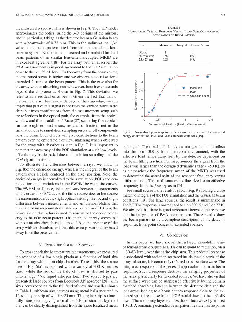
Fig. 8. (a) Radial mean of beam pattern. Shown is the median of ∼20 pixels from the array center. (b) Zoom on the radial mean. (c) Encircled energy, the integralof the beam pattern to a given radius centered on each pixel. The encircled energy is the median value of ∼20 central pixels, normalized to the total power of thePOP simulation and corrected for slightly different beam radii (see text for details).
field of view. For each xy point, typically 1 s of data is recorded.The hot source temperature is adjusted so the maximum sig-nal during the measurement matches the MKID instantaneousdynamic range. This is taken in MKID phase readout [3], [23]as ∼1 rad. with respect to the MKID resonance circle in thecomplex plane. In postprocessing, the data are calibrated to aneffective frequency shift via the MKID phase signal using thestrategy outlined in [24]. This linearizes the signal with respectto the optical power and removes responsivity changes due todrifts in the optical loading. This results in reproducible beamsfor different source powers, MKID readout tone frequencies andpowers. The position-dependent response is determined by ap-plying a flat-top windowed fast Fourier transform (FFT) to eachsecond of MKID frequency response and taking the FFT ampli-tude at the chopper frequency. Since the chopper is not locked,it has a slight frequency drift. To correct for this, we modulate afew off-KID readout tones using analogue electronics with theexact chopper frequency. This gives the exact chopper frequencyin the measured data, enabling drift correction in postprocess-ing. This was implemented only for the array with absorber. Forthe array without absorber, we use the sum of all MKIDs for thispurpose: The pedestal response ensures that a signal is presentindependent of the source position.
The position-dependent responses is shown in Fig. 1(a) forthe array without absorbing mesh, and in Fig. 1(b), for the ar-ray with absorbing mesh. In both figures, we give the correctedresponse Pc , given by Pc =
√P 2 − P 2
n , where P 2n is the mean
value of the signal with the hot source outside of the field ofview of the cryostat optics. The square is needed because theKID noise, readout noise, and photon noise contributions all addin P 2 , with P the measured signal. We observe a significant re-duction ( 10 dB) in the pedestal response for the array with meshabsorber. To make this even clearer, we show in Fig. 8(a) and (b),the radial mean of the beam pattern. The radial mean averagesthe beam pattern over a circle centered on the pixel position, soimproving on the signal to noise of the beam pattern. The solid(blue) line, representing the data without a mesh absorber, is
10 dB above the (red) dashed line, representing the data with anabsorber, for radii in excess of 20 mm.
The measured beam pattern, as shown in Fig. 1(b), has a noisefloor at ∼−35 dB. This is not sufficient to measure the residualresponse for the array with absorber. For these reasons, we haveperformed an additional measurement using a harmonic sourceand a multiplier chain in a heterodyne configuration givingthe phase and amplitude (P&A) beam patterns [25], similar tothe method presented in Davis et al. [26]. The multiplier chainis used as a stationary local oscillator that is coupled to theentire the array with a thin mylar beam splitter. The harmonicmixer is scanned in the reimaged focal plane. The sources areoperated at a small, ∼424 Hz, offset modulating the signal. Themagnitude and phase of this modulation gives the amplitude andphase of the system beam pattern, with only the amplitude pre-sented here. The scanned positions in xy plane are chosen to beevery 1 mm, less than FWHM/4, the full-width half-maximumbeamwidth, to resolve the beam shape in more detail. Due tothe dual-source modulation, the P&A measurement measuresthe amplitude of the beam pattern whereas the hot source givesthe power [25]. This means the P&A measurement dynamicrange is square of that with the hot source for the same mod-ulation level, giving a noise floor of � −60 dB, as shown inFig 7. Additionally the harmonic mixer uses a thin-walled openwaveguide to launch the radiation; so it is a single-mode, single-polarization, and a single-frequency point source with an nearisotropic beam pattern. The pattern measured with this sourcecan therefore directly be compared to simulations. With thisextra dynamic range, we clearly observe in the 2-D beam pat-tern that even with an on-chip absorber, a residual large arearesponse is still visible at a −40 to −50-dB level.
IV. COMPARISON TO OPTICAL SIMULATION
To further assess the measured performance and to compare itto the theoretical performance, we take a POP simulation of thecamera cryostat optics and compare this to the radial mean of
YATES et al.: SURFACE WAVE CONTROL FOR LARGE ARRAYS OF MKIDs 795
the measured response. This is shown in Fig. 8. The POP modelapproximates the optics, using the 3-D designs of the mirrors,and in particular, taking as the detector beam a Gaussian beamwith a beamwaist of 0.72 mm. This is the radius at the 1/e2
value of the beam pattern fitted from simulations of the lens-antenna system. Note that the measured and simulated far-fieldbeam patterns of an similar lens-antenna-coupled MKID arein excellent agreement [8]. For the array with an absorber, theP&A measurement is in good agreement to the POP simulationdown to the∼−35-dB level. Further away from the beam center,the measured signal is higher and we observe a clear low-levelextended feature on the beam pattern. This is the case also forthe array with an absorbing mesh, however, here it even extendsbeyond the chip area as shown in Fig. 7. This deviation werefer to as a residual error beam. Given the fact that part ofthe residual error beam extends beyond the chip edge, we canimply that part of this signal is not from the surface wave in thechip, but from contributions from the measurement setup suchas: reflections in the optical path, for example, from the opticalwindow and filters; additional Ruze [27] scattering from opticalsurface roughness and errors; residual diffraction, not in thesimulation due to simulation sampling errors or off componentsnear the beam. Such effects will give contributions to the beampattern over the optical field of view, matching what is observedfor the array with absorber as seen in Fig. 7. It is important tonote that the accuracy of the POP simulation at such low levels,off axis may be degraded due to simulation sampling and thePOP algorithm itself.
To illustrate the difference between arrays, we show inFig. 8(c) the encircled energy, which is the integral of the beampattern over a circle centered on the pixel position. Note, theencircled energy is normalized to the simulation (POP) and cor-rected for small variations in the FWHM between the curves.The FWHM, and hence, its integral vary between measurementson the order of ∼10% due to the finite source size for hot sourcemeasurements, defocus, slight optical misalignments, and slightdifference between measurements and simulation. Noting thatthe main beam response dominates up to a radius of 10 mm, thepower inside this radius is used to normalize the encircled en-ergy to the POP beam pattern. The encircled energy shows thatwithout an absorber, there is almost 1.6 × the response of thearray with an absorber, and that this extra power is distributedaway from the pixel center.
V. EXTENDED SOURCE RESPONSE
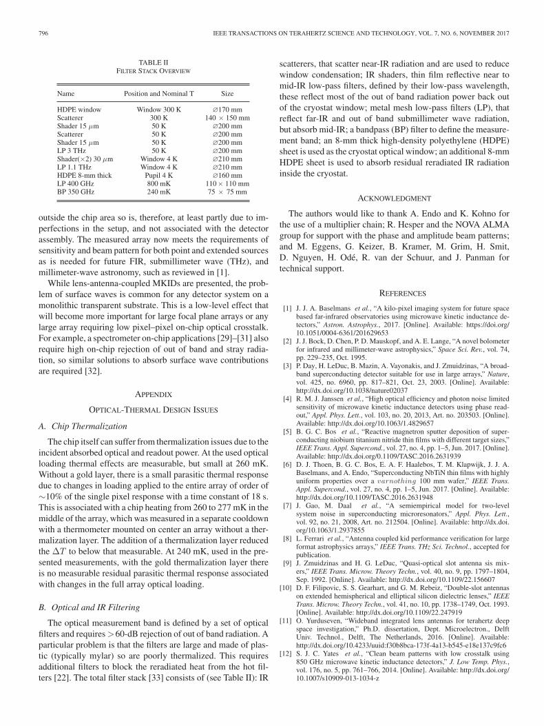
To cross check the beam pattern measurements, we measuredthe response of a few single pixels as a function of load sizefor the array with an on-chip absorber. To test this, the source[see in Fig. 6(a)] is replaced with a variety of 300-K sourcessizes, while the rest of the field of view is allowed to passonto a large 77-K liquid nitrogen load. Two source types arepresented: large sources from Eccosorb AN absorber [28], withsizes corresponding to the full field of view and smaller shownin Table I; subbeam size sources using metal balls mounted to12-μm mylar strip of width ∼20 mm. The mylar strip is almostfully transparent, giving a small, ∼5-K constant backgroundthat can be clearly distinguished from the more localized metal
TABLE INORMALIZED OPTICAL RESPONSE VERSUS LOAD SIZE, COMPARED TO
INTEGRATION OF BEAM PATTERN
Load Measured Integral of Beam Pattern
300 K 1 130 mm strip 0.92 0.9325×25 mm 0.89 0.85
Fig. 9. Normalized peak response versus source size, compared to encircledenergy of simulation, POP, and Gaussian beam equations [19].
ball signal. The metal balls block the nitrogen load and reflectinto the beam 300 K from the room environment, with theeffective load temperature seen by the detector dependent onthe beam filling fraction. For large sources the signal from theloads was larger than the designed dynamic range (∼50 K), soas a crosscheck the frequency sweep of the MKID was usedto determine the actual shift of the resonant frequency versusdifferent loads. The small sources are linearized to an effectivefrequency from the f-sweep as in [24].
For small sources, the result is shown Fig. 9 showing a closematch to integrals of the POP simulation and the Gaussian beamequations [19]. For large sources, the result is summarized inTable I. The response is normalized to 1 on 300 K and 0 on 77 K.We observe that there is good agreement between the responseand the integration of P&A beam pattern. These results showthe beam pattern to be a complete description of the detectorresponse, from point sources to extended sources.
VI. CONCLUSION
In this paper, we have shown that a large, monolithic arrayof lens-antenna-coupled MKIDs can respond to radiation, on a−30-dB level, over the entire chip area. This pedestal responseis associated with radiation scattered inside the dielectric of thearray substrate, it is commonly referred to as a surface wave. Theintegrated response of the pedestal approaches the main beamresponse. Such a response destroys the imaging properties ofthe array, particularly for extended sources. We have shown thatthe surface wave can be suppressed effectively by including amatched absorbing layer in between the detector chip and thelens array, leading to a beam pattern response close to the ex-pected spatial response from a POP model down to the −35-dBlevel. The absorbing layer reduces the surface wave by at least10 dB. A remaining extended beam pattern feature has response
796 IEEE TRANSACTIONS ON TERAHERTZ SCIENCE AND TECHNOLOGY, VOL. 7, NO. 6, NOVEMBER 2017
TABLE IIFILTER STACK OVERVIEW
Name Position and Nominal T Size
HDPE window Window 300 K ∅170 mmScatterer 300 K 140 × 150 mmShader 15 μm 50 K ∅200 mmScatterer 50 K ∅200 mmShader 15 μm 50 K ∅200 mmLP 3 THz 50 K ∅200 mmShader(×2) 30 μm Window 4 K ∅210 mmLP 1.1 THz Window 4 K ∅210 mmHDPE 8-mm thick Pupil 4 K ∅160 mmLP 400 GHz 800 mK 110× 110 mmBP 350 GHz 240 mK 75 × 75 mm
outside the chip area so is, therefore, at least partly due to im-perfections in the setup, and not associated with the detectorassembly. The measured array now meets the requirements ofsensitivity and beam pattern for both point and extended sourcesas is needed for future FIR, submillimeter wave (THz), andmillimeter-wave astronomy, such as reviewed in [1].
While lens-antenna-coupled MKIDs are presented, the prob-lem of surface waves is common for any detector system on amonolithic transparent substrate. This is a low-level effect thatwill become more important for large focal plane arrays or anylarge array requiring low pixel–pixel on-chip optical crosstalk.For example, a spectrometer on-chip applications [29]–[31] alsorequire high on-chip rejection of out of band and stray radia-tion, so similar solutions to absorb surface wave contributionsare required [32].
APPENDIX
OPTICAL-THERMAL DESIGN ISSUES
A. Chip Thermalization
The chip itself can suffer from thermalization issues due to theincident absorbed optical and readout power. At the used opticalloading thermal effects are measurable, but small at 260 mK.Without a gold layer, there is a small parasitic thermal responsedue to changes in loading applied to the entire array of order of∼10% of the single pixel response with a time constant of 18 s.This is associated with a chip heating from 260 to 277 mK in themiddle of the array, which was measured in a separate cooldownwith a thermometer mounted on center an array without a ther-malization layer. The addition of a thermalization layer reducedthe ΔT to below that measurable. At 240 mK, used in the pre-sented measurements, with the gold thermalization layer thereis no measurable residual parasitic thermal response associatedwith changes in the full array optical loading.
B. Optical and IR Filtering
The optical measurement band is defined by a set of opticalfilters and requires >60-dB rejection of out of band radiation. Aparticular problem is that the filters are large and made of plas-tic (typically mylar) so are poorly thermalized. This requiresadditional filters to block the reradiated heat from the hot fil-ters [22]. The total filter stack [33] consists of (see Table II): IR
scatterers, that scatter near-IR radiation and are used to reducewindow condensation; IR shaders, thin film reflective near tomid-IR low-pass filters, defined by their low-pass wavelength,these reflect most of the out of band radiation power back outof the cryostat window; metal mesh low-pass filters (LP), thatreflect far-IR and out of band submillimeter wave radiation,but absorb mid-IR; a bandpass (BP) filter to define the measure-ment band; an 8-mm thick high-density polyethylene (HDPE)sheet is used as the cryostat optical window; an additional 8-mmHDPE sheet is used to absorb residual reradiated IR radiationinside the cryostat.
ACKNOWLEDGMENT
The authors would like to thank A. Endo and K. Kohno forthe use of a multiplier chain; R. Hesper and the NOVA ALMAgroup for support with the phase and amplitude beam patterns;and M. Eggens, G. Keizer, B. Kramer, M. Grim, H. Smit,D. Nguyen, H. Ode, R. van der Schuur, and J. Panman fortechnical support.
REFERENCES
[1] J. J. A. Baselmans et al., “A kilo-pixel imaging system for future spacebased far-infrared observatories using microwave kinetic inductance de-tectors,” Astron. Astrophys., 2017. [Online]. Available: https://doi.org/10.1051/0004-6361/201629653
[2] J. J. Bock, D. Chen, P. D. Mauskopf, and A. E. Lange, “A novel bolometerfor infrared and millimeter-wave astrophysics,” Space Sci. Rev., vol. 74,pp. 229–235, Oct. 1995.
[3] P. Day, H. LeDuc, B. Mazin, A. Vayonakis, and J. Zmuidzinas, “A broad-band superconducting detector suitable for use in large arrays,” Nature,vol. 425, no. 6960, pp. 817–821, Oct. 23, 2003. [Online]. Available:http://dx.doi.org/10.1038/nature02037
[4] R. M. J. Janssen et al., “High optical efficiency and photon noise limitedsensitivity of microwave kinetic inductance detectors using phase read-out,” Appl. Phys. Lett., vol. 103, no. 20, 2013, Art. no. 203503. [Online].Available: http://dx.doi.org/10.1063/1.4829657
[5] B. G. C. Bos et al., “Reactive magnetron sputter deposition of super-conducting niobium titanium nitride thin films with different target sizes,”IEEE Trans. Appl. Supercond., vol. 27, no. 4, pp. 1–5, Jun. 2017. [Online].Available: http://dx.doi.org/0.1109/TASC.2016.2631939
[6] D. J. Thoen, B. G. C. Bos, E. A. F. Haalebos, T. M. Klapwijk, J. J. A.Baselmans, and A. Endo, “Superconducting NbTiN thin films with highlyuniform properties over a varnothing 100 mm wafer,” IEEE Trans.Appl. Supercond., vol. 27, no. 4, pp. 1–5, Jun. 2017. [Online]. Available:http://dx.doi.org/10.1109/TASC.2016.2631948
[7] J. Gao, M. Daal et al., “A semiempirical model for two-levelsystem noise in superconducting microresonators,” Appl. Phys. Lett.,vol. 92, no. 21, 2008, Art. no. 212504. [Online]. Available: http://dx.doi.org/10.1063/1.2937855
[8] L. Ferrari et al., “Antenna coupled kid performance verification for largeformat astrophysics arrays,” IEEE Trans. THz Sci. Technol., accepted forpublication.
[9] J. Zmuidzinas and H. G. LeDuc, “Quasi-optical slot antenna sis mix-ers,” IEEE Trans. Microw. Theory Techn., vol. 40, no. 9, pp. 1797–1804,Sep. 1992. [Online]. Available: http://dx.doi.org/10.1109/22.156607
[10] D. F. Filipovic, S. S. Gearhart, and G. M. Rebeiz, “Double-slot antennason extended hemispherical and elliptical silicon dielectric lenses,” IEEETrans. Microw. Theory Techn., vol. 41, no. 10, pp. 1738–1749, Oct. 1993.[Online]. Available: http://dx.doi.org/10.1109/22.247919
[11] O. Yurduseven, “Wideband integrated lens antennas for terahertz deepspace investigation,” Ph.D. dissertation, Dept. Microelectron., DelftUniv. Technol., Delft, The Netherlands, 2016. [Online]. Available:http://dx.doi.org/10.4233/uuid:f30b8bca-173f-4a13-b545-e18e137c9fc6
[12] S. J. C. Yates et al., “Clean beam patterns with low crosstalk using850 GHz microwave kinetic inductance detectors,” J. Low Temp. Phys.,vol. 176, no. 5, pp. 761–766, 2014. [Online]. Available: http://dx.doi.org/10.1007/s10909-013-1034-z
YATES et al.: SURFACE WAVE CONTROL FOR LARGE ARRAYS OF MKIDs 797
[13] A. Adane et al., “Crosstalk in a KID array caused by the thickness variationof superconducting metal,” J. Low Temp. Phys., vol. 184, no. 1, pp. 137–141, Jul. 2016. [Online]. Available: http://dx.doi.org/10.1007/s10909-016-1490-3
[14] L. Bisigello, S. J. C. Yates, L. Ferrari, J. J. A. Baselmans, and A. Baryshev,“Measurements and analysis of optical crosstalk in a microwave kineticinductance detector array,” Proc. SPIE, vol. 9914, 2016, Art. no. 99143L.[Online]. Available: http://dx.doi.org/10.1117/12.2238643
[15] F. Schrey, R. Mathis, and R. Payne, “Structure and properties of RFsputtered, superconducting tantalum films,” Thin Solid Films, vol. 5, no. 1,pp. 29–40, 1970.
[16] M. Mohazzab, N. Mulders, A. Nash, and M. Larson, “Tantalum thin-film superconducting transition edge thermometers,” J. Low Temp. Phys.,vol. 121, no. 5–6, pp. 821–824, 2000.
[17] Dassault Systemes, “CST Microwave Studio.” [Online]. Available:https://www.cst.com
[18] J. van Rantwijk, M. Grim, D. van Loon, S. Yates, A. Baryshev,and J. Baselmans, “Multiplexed readout for 1000-pixel arrays of mi-crowave kinetic inductance detectors,” IEEE Trans. Microw. TheoryTechn., vol. 64, no. 6, pp. 1876–1883, Jun. 2016. [Online]. Available:http://dx.doi.org/10.1109/TMTT.2016.2544303
[19] P. F. Goldsmith, Gaussian Beam Quasioptical Propagation and Applica-tions. Piscataway, NJ, USA: IEEE Press, 1998.
[20] J. A. Murphy, “Distortion of a simple Gaussian beam on reflec-tion from off-axis ellipsoidal mirrors,” Int. J. Infrared MillimeterWaves, vol. 8, no. 9, pp. 1165–1187, Sep. 1987. [Online]. Available:http://dx.doi.org/10.1007/BF01010819
[21] Zemax LLC, “Zemax optical studio,” 2013. [Online]. Available: www.zemax.com
[22] C. Tucker and P. Ade, “Thermal filtering for large aperture cryogenic de-tector arrays,” Proc. SPIE, vol. 6275, pp. 6275-1–6275-9, 2006. [Online].Available: http://dx.doi.org/10.1117/12.673159
[23] J. Gao, J. Zmuidzinas, B. A. Mazin, H. G. LeDuc, and P. K. Day,“Noise properties of superconducting coplanar waveguide microwave res-onators,” Appl. Phys. Lett., vol. 90, no. 10, 2007. [Online]. Available:http://scitation.aip.org/content/aip/journal/apl/90/10/10.1063/1.2711770
[24] L. Bisigello, S. J. C. Yates, V. Murugesan, J. J. A. Baselmans,and A. M. Baryshev, “Calibration scheme for large kinetic induc-tance detector arrays based on readout frequency response,” J. LowTemp. Phys., vol. 184, no. 1, pp. 161–166, 2016. [Online]. Available:http://dx.doi.org/10.1007/s10909-016-1524-x
[25] C. N. Thomas and S. Withington, “Experimental demonstration of an inter-ferometric technique for characterizing the full optical behavior of multi-mode power detectors,” IEEE Trans. THz Sci. Technol., vol. 2, no. 1,pp. 50–60, Jan. 2012. [Online]. Available: http://dx.doi.org/10.1109/TTHZ.2011.2177693
[26] K. K. Davis et al., “Proof-of-concept demonstration of vector beam patternmeasurements of kinetic inductance detectors,” IEEE Trans. THz Sci.Technol., vol. 7, no. 1, pp. 98–106, Jan. 2017. [Online]. Available: http://dx.doi.org/10.1109/TTHZ.2016.2617869
[27] J. Ruze, “Antenna tolerance theory #8212;a review,” Proc. IEEE, vol. 54,no. 4, pp. 633–640, Apr. 1966. [Online]. Available: http://dx.doi.org/10.1109/PROC.1966.4784
[28] Emerson & Cuming Microw. Products, Inc., “ECCOSORB AN absorber.”[Online]. Available: www.eccosorb.com
[29] A. Endo et al., “Design of an integrated filterbank for DESHIMA: On-chipsubmillimeter imaging spectrograph based on superconducting res-onators,” J. Low Temp. Phys., vol. 167, pp. 341–346, 2012. [Online].Available: http://dx.doi.org/10.1007/s10909-012-0502-1
[30] S. Hailey-Dunsheath et al., “Low noise titanium nitride kids for superspec:A millimeter-wave on-chip spectrometer,” J. Low Temp. Phys., vol. 184,no. 1, pp. 180–187, 2016. [Online]. Available: http://dx.doi.org/10.1007/s10909-015-1375-x
[31] G. Cataldo, W.-T. Hsieh, W.-C. Huang, S. H. Moseley, T. R. Stevenson, andE. J. Wollack, “Micro-spec: An ultracompact, high-sensitivity spectrom-eter for far-infrared and submillimeter astronomy,” Appl. Opt., vol. 53,no. 6, pp. 1094–1102, Feb. 2014. [Online]. Available: http://ao.osa.org/abstract.cfm?URI=ao-53-6-1094
[32] E. M. Barrentine et al., “Design and performance of a high resolutionμ spec: An integrated sub-millimeter spectrometer,” Proc. SPIE, vol. 9914,p. 99143O, 2016. [Online]. Available: http://dx.doi.org/10.1117/12.22-34462
[33] QMC Instruments Ltd., School Phys. Astron., Cardiff Univ., Cardiff, U.K.[Online]. Available: www.terahertz.co.uk
Stephen J. C. Yates received the Ph.D. degree fromthe University of Bristol, Bristol, U.K., in 2003, work-ing on experimental low-temperature techniques forcondensed matter physics.
He was with CNRS-CRTBT (now Insti-tut Nel), Grenoble, France, as a PostdoctoralResearcher involved with low-temperature mag-netism and superconductivity (2003–2004) and thenwith the development of low-temperature detectorsand techniques for astrophysics (2004–2006). He iscurrently an Instrument Scientist involved with su-
perconducting microwave kinetic inductance detectors (MKIDs) with SRON,The Netherlands Institute for Space Research, Groningen, The Netherlands,which he joined in 2006. His current interests include MKID development forsubmillimeter applications, but also include a wider interest in device physicsand superconductivity, optical design, and full end-to-end instrument character-ization and performance. He has authored or co-authored more than 50 papers.
Andrey M. Baryshev received the M.S. degree(summa cum laude) in physical quantum electron-ics from the Moscow Physical Technical Institute,Moscow, Russia, in 1993, and the Ph.D. degree insuperconducting integrated receiver combining SISmixers and flux flow oscillatoron into one chip fromthe Technical University of Delft, Delft, The Nether-lands, in 2005.
He currently an Associate Professor withthe Kapteyn Astronomical Institute, University ofGroningen, Groningen, Netherlands. He was previ-
ously a Senior Instrument Scientist with the SRON Low Energy AstrophysicsDivision, Groningen, from 1998 to 2017. In 1993, he was an Instrument Sci-entist with the Institute of Radio Engineering and Electronics, Moscow, wherehe was involved in the field of sensitive superconducting heterodyne detectors.In 2000, he joined an effort to develop an SIS receiver (600–720 GHz) for theatacama large millimeter array, where he designed the SIS mixer, quasi-opticalsystem, and contributed to a system design. His current main research interestsinclude application heterodyne and direct detectors for large focal plane arraysin terahertz frequencies and quasi-optical systems design and experimental ver-ification.
Dr. Baryshev was the recipient of the NWO-VENI Grant for his researchon heterodyne focal plane arrays technology in 2008, and in 2009, he was therecipient of the EU Commission Starting Researcher Grant for his research onfocal plane arrays of direct detectors.
Ozan Yurduseven (S’11) received the B.Sc. andM.Sc. degrees (Hons.) in electronics and communica-tions engineering from Yildiz Technical University,Istanbul, Turkey, in 2009 and 2011, respectively, andthe Ph.D. degree in electrical engineering from theDelft University of Technology, Delft, The Nether-lands, in 2016, with research on the development ofthe dielectric lens antennas for terahertz space appli-cations.
During his Ph.D. studies, he spent six months as aVisiting Researcher with the Instituto de Telecomuni-
caes, Instituto Superior Tecnico, Lisbon, Portugal, where he was involved withthe double shell dielectric lenses. He has authored or coauthored more than 30publications in peer-reviewed journals and conferences. His current research in-terests include dielectric lens antennas for millimeter- and submillimeter-wavespace applications, quasi-optical systems, numerical techniques in electromag-netics, and metamaterials.
Dr. Yurduseven is a member of the IEEE Antennas and Propagation Societyand the European Association on Antennas and Propagation. He was the recip-ient of the Best Student Paper Award of the European Conference on Antennasand Propagation (EuCAP) in 2013. He is one of the coauthors of the confer-ence proceeding that received the Best Paper Award on Electromagnetism andAntenna Theory at EuCAP 2016. He serves as a Reviewer for the IEEE TRANS-ACTIONS ON ANTENNAS AND PROPAGATION, IEEE ANTENNAS AND WIRELESS
PROPAGATION LETTERS, and IET Microwaves, Antennas and Propagation.

798 IEEE TRANSACTIONS ON TERAHERTZ SCIENCE AND TECHNOLOGY, VOL. 7, NO. 6, NOVEMBER 2017
Juan Bueno received the graduate degree in physicsfrom the University of Cantabria, Santander, Spain,in 2003 and the Ph.D. degree in quantum crystals atvery low temperatures from the University of Leiden,Leiden, The Netherlands, in 2007.
From 2007 to 2008, he was a Postdoctoral Fel-low with the University of California at San Diego,La Jolla, CA, USA, continuing his work on quantumcrystals. In 2008, he made the decision to switch re-search topics and interests from fundamental physicsto the study of superconducting devices. He was
awarded with a NASA postdoctoral position, becoming a Postdoctoral Fel-low with the Jet Propulsion Laboratory (JPL), Pasadena, CA, USA, until 2010.During this time, he pioneered a new type of pair-breaking radiation detector, thequantum capacitance detector. After his time with the JPL, he joined the Cen-ter for Astrobiology (Spain) in 2010 after receiving a JAE-doc grant, workingmainly on kinetic inductance detectors (KIDs). He became an Instrument Scien-tist in 2012 with SRON, The Netherlands Institute for Space Research, Utrecht,The Netherlands, working on the development of KIDs for submillimeter-waveand far IR space-based observatories. He has authored or co-authored morethan 30 peer-reviewed papers, a third of them as the lead author. His researchinterest include the development of ultrasensitive broadband KIDs for futurespace-based missions.
Kristina K. Davis received the B.A. degree in as-tronomy from the University of Colorado, Boulder,CO, USA, in 2012. She is currently working towardthe Ph.D. degree at Arizona State University, Tempe,AZ, USA, in exploration systems design, with a con-centration in instrumentation.
Since becoming a graduate student in 2012, herresearch has focused on the design, fabrication, cal-ibration and testing, and data analysis for astronom-ical missions in the terahertz frequency regime. Hermain research focus radiation pattern measurement
techniques and analysis. Her research interests include to design ground, atmo-spheric, and space-based instruments to study the lifecycle of the gas and dustin the interstellar medium.
Lorenza Ferrari received the Ph.D. degree in ap-plied physics from the University of Genoa, Genoa,Italy, in 2009, working on cryogenic detectors for as-trophysics applications.
After she worked for one year with the INFNGenoa and PTB Berlin, Germany, as a PostdoctoralResearcher on low-temperature detectors for neutrinomass experiments. Since 2010, she has been an In-strument Scientist with SRON, The Netherlands In-stitute for Space Research, Groningen, Netherlands.Her current research interests include the develop-
ment of microwave kinetic inductance detectors for submillimeter applicationsand transition edge sensors for far infrared frequency range focusing on opticalcharacterization and application in scientific instruments. She is also involved inthe SpicA FAR-infrared Instrument and X-ray Integral Field Unit spectrometerexperiments modeling and testing the focal plane assembly, as well as designingcryogenic facilities for performance validation of instruments components.
Willem Jellema received the M.Sc. degree in appliedphysics from the University of Groningen, Gronin-gen, The Netherlands, in 1998, and the Ph.D. degreein applied physics from the Faculty of Mathemat-ics and Natural Sciences, University of Groningen,Groningen, in 2015, on the optical design and perfor-mance verification of Herschel-HIFI.
He currently holds the title of Systems EngineerELT Instrumentation with The Netherlands ResearchSchool for Astronomy, Dwingeloo, The Netherlands.Previously, he was a Senior Instrument Scientist with
SRON, The Netherlands Institute for Space Research, Groningen, where hehas been since 1998. From 1998 to 2015, he was an Instrument Scientist in-volved with the Herschel-HIFI project, responsible for the end-to-end opticaldesign verification, alignment, and calibration. Since 2009, he has been the In-strument Scientist of SPICA-Safari, a far-infrared spectrometer proposed for alarge aperture cryogenic telescope in space. In 2014, he also became the LeadSystems Engineer of SPEX, an optical multiangle spectropolarimeter for futureatmospheric missions. In November 2017, he joined NOVA to support the de-velopment of the METIS, MICADO, and MOSAIC instruments for the E-ELT.He has been involved in various other projects related to the development, en-gineering, and calibration of submillimeter wave and optical instrumentationfor space and has a special interest in long-wave diffractive optics and coherentheterodyne technologies and applications.
Nuria Llombart (S’06–M’07–SM’13) received theElectrical Engineering and Ph.D. degrees from thePolytechnic University of Valencia, Valencia, Spain,in 2002 and 2006, respectively.
During her Master’s degree studies, she spentone year with the Friedrich-Alexander University ofErlangen–Nuremberg, Erlangen, Germany, and waswith the Fraunhofer Institute for Integrated Circuits,Erlangen. From 2002 to 2007, she was with the An-tenna Group, TNO Defence, Security and Safety In-stitute, The Hague, The Netherlands, as a Ph.D. stu-
dent and then a Researcher. From 2007 to 2010, she was a Postdoctoral Fellowwith the California Institute of Technology with the Submillimeter Wave Ad-vance Technology Group, Jet Propulsion Laboratory (JPL), Pasadena, CA, USA.She was a Ramn y Cajal Fellow with the Optics Department, Complutense Uni-versity of Madrid, Spain, from 2010 to 2012. In September 2012, she joinedthe THz Sensing Group, Technical University of Delft, Delft, The Netherlands,where she is currently an Associate Professor. She has co-authored more than150 journal and international conference contributions. Her research interestsinclude the analysis and design of planar antennas, periodic structures, reflec-tor antennas, lens antennas, and waveguide structures with an emphasis in theterahertz range.
Dr. Llombart was the corecipient of the H. A. Wheeler Award for the BestApplications Paper of 2008 in the IEEE TRANSACTIONS ON ANTENNAS AND
PROPAGATION, the 2014 THz Science and Technology Best Paper Award of theIEEE Microwave Theory and Techniques Society and several NASA awards.She was also the recipient of the 2014 IEEE Antenna and Propagation Soci-ety Lot Shafai Mid-Career Distinguished Achievement Award. She serves as aBoard member of the IRMMW-THz International Society. In 2015, she was therecipient of the European Research Council (ERC) Starting Grant.

YATES et al.: SURFACE WAVE CONTROL FOR LARGE ARRAYS OF MKIDs 799
Vignesh Murugesan received the M.Sc. degreein microsystem integration technology from theChalmers University of Technology, Gothenburg,Sweden, in 2007.
He was a Process Integration Engineer from 2007to 2008 with Infineon Technologies AG, Regensburg,Germany. From 2010 to 2013, he was a MEMS Pro-cess Engineer with Thermo Fisher Scientific, En-schede, The Netherlands. Since 2013, he has beena Process Engineer with SRON, The Netherlands In-stitute for Space Research, Utrecht, The Netherlands,
working with the Microwave Kinetic Inductance Detectors Group. He is cur-rently responsible for the fabrication and process development of microwavekinetic inductance detectors chips.
David J. Thoen was born in Nieuwveen, TheNetherlands, in 1978. He received the B.S. degree inapplied physics from the Fontys University of Tech-nology, Eindhoven, The Netherlands, in 2008.
He started in 2007 as a Microwave Engineer withthe Dutch Institute for Fundamental Energy Research(formerly known as the FOM Institute Rijnhuizen),Nieuwegein, The Netherlands, where he was involvedwith microwave diagnostics for real-time control ofelectron–cyclotron resonance heating of nuclear fu-sion plasmas in tokamaks. In 2010, he joined the
Cosmo Nanoscience group, Delft University of Technology, Delft, The Nether-lands, where he was involved with the development and fabrication of the Band9 (600–720 GHz) superconductor/insulator/superconductor detector chips ofthe Atacama Large Millimeter Array. Since 2012, he has been involved withmicrowave kinetic inductance detectors (MKIDs), from 2015, with the Tera-hertz Sensing Group, Delft University of Technology. He is responsible for thedevelopment and processing of the MKID in the Kavli cleanroom, Delft. Hisfocus is reactive sputtering of niobium-titanium-nitride and quality control ofthin films. He coauthored more than 20 peer-reviewed papers.
Jochem J. A. Baselmans received the graduated de-gree and Ph.D. degree (summa cum laude) in con-trollable Josephson junctions from the University ofGroningen, Groningen, The Netherlands, in 1998 and2002, respectively.
He is a Senior Instrument Scientist with theSRON, The Netherlands Institute for Space Research,Utrecht, The Netherlands, where he has been withthe Technology Division since 2002. Since 2015, hehas been an Associate Professor with the THz Sens-ing Group, Delft University of Technology, Delft,
The Netherlands. In 2002, he became a Postdoctoral Instrument Scientist withSRON, The Netherlands Institute for Space Research, where, until 2004, hewas involved with on hot electron bolometer mixers, very sensitive hetero-dyne radiation detectors for frequencies between 1–5 THz. In 2005, he joinedSRON, Utrecht, and began working with microwave kinetic inductance detectors(MKIDs) after a three-month visit with the California Institute of Technology,Pasadena, CA, USA. He now leads the Dutch effort on the development ofMKIDs. He has authored or co-authored more than 100 papers.
Dr. Baselmans was the recipient of an ERC Consolidator Grant to developan advanced imaging spectrometer based upon MKIDs in 2015.