university of michigan eecs 522: analog integrated ... · pdf fileuniversity of michigan eecs...
TRANSCRIPT

University of Michigan EECS 522: Analog Integrated Circuits
Winter 2009
Final Exam
April 28, 2009
NAME: ________________________________________________ Honor Code: I have neither given nor received unauthorized aid on this examination, nor have I concealed any violations of the Honor Code. Signature _____________________________________
Problem Points Score Initials
1 22
2 22
3 22
4 22
5 12
Total

Page 2 of 17

Initials: ____________
Page 3 of 17
Problem 1 (22 Points): Potpourri. This problem has 3 unrelated parts. a) Derive an expression for the conversion gain of the mixer shown below. Assume the LO
amplitude is much larger than the RF amplitude, and that the diodes are ideal and switch instantaneously.
Page 4 of 17
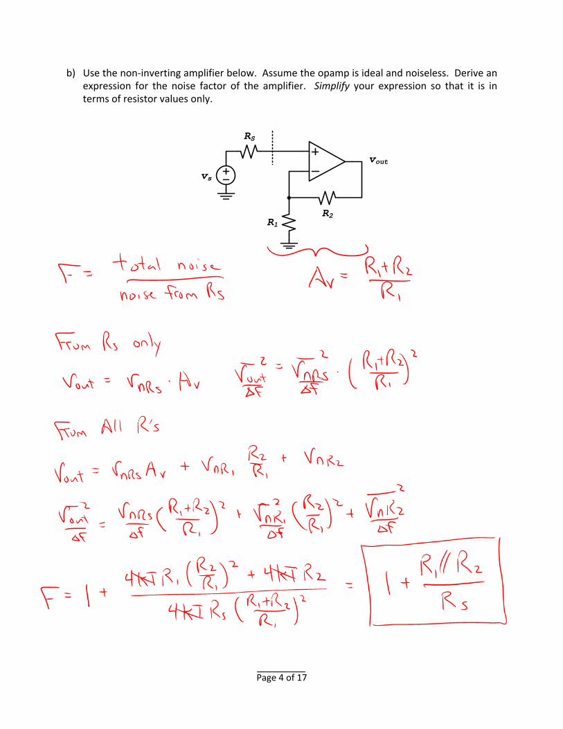
b) Use the non‐inverting amplifier below. Assume the opamp is ideal and noiseless. Derive an expression for the noise factor of the amplifier. Simplify your expression so that it is in terms of resistor values only.
vout
vs
RS
R2R1
Initials: ____________
Page 5 of 17
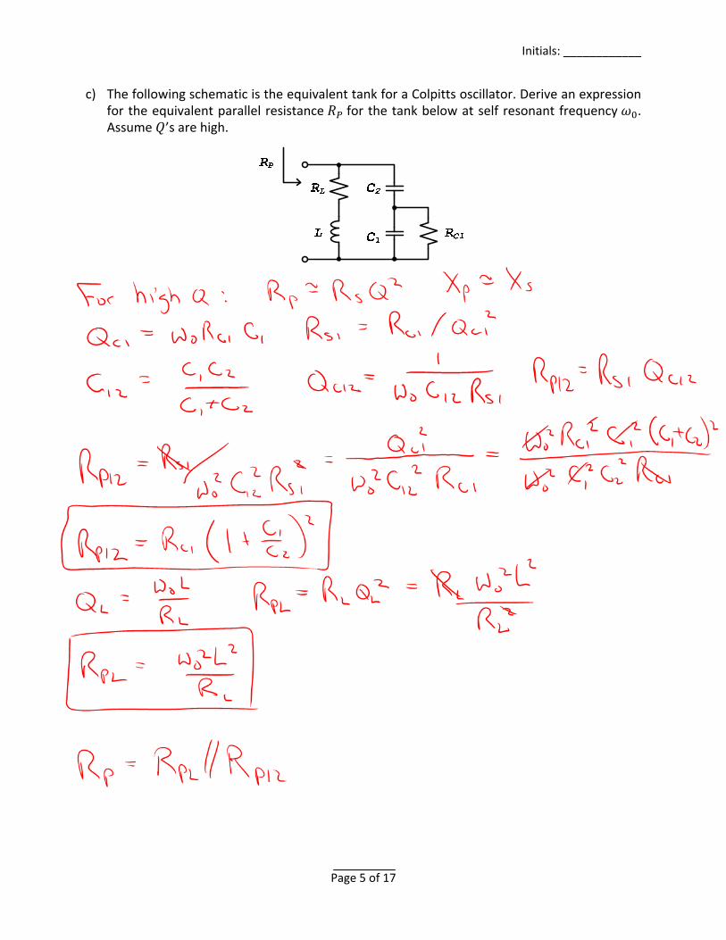
c) The following schematic is the equivalent tank for a Colpitts oscillator. Derive an expression for the equivalent parallel resistance for the tank below at self resonant frequency . Assume ’s are high.
Page 6 of 17
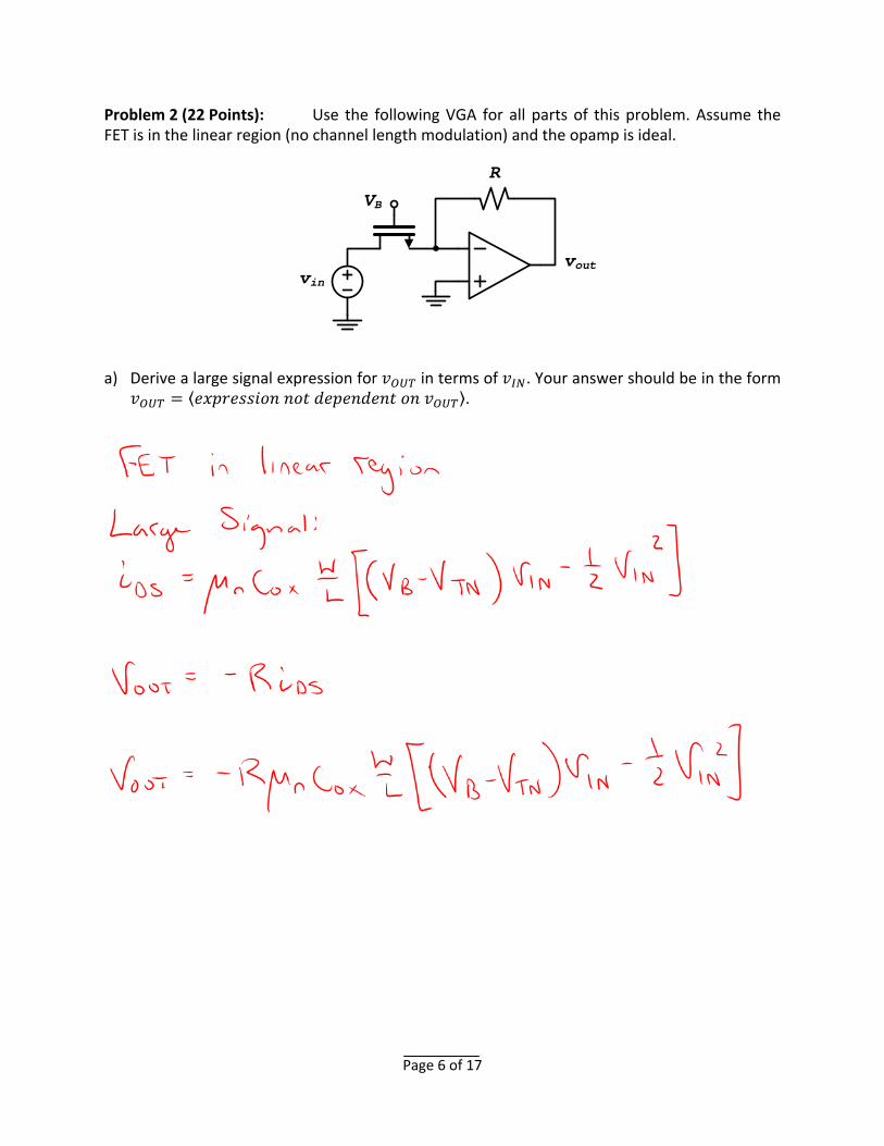
Problem 2 (22 Points): Use the following VGA for all parts of this problem. Assume the FET is in the linear region (no channel length modulation) and the opamp is ideal. a) Derive a large signal expression for in terms of . Your answer should be in the form
.
R
vin
vout
VB

Initials: ____________
Page 7 of 17
b) Derive expressions for the and terms where . The general expression for the Taylor Series given below, where is the nth derivative of , evaluated at .
!
Page 8 of 17
c) Derive an expression for the input‐referred 2nd‐order intercept point IIP2. You answer may be in terms of and . The IIP2 is defined for a two‐tone test as the input amplitude at which the intermodulation amplitude (term at sum/difference frequency) is equal to the fundamental amplitude.

Initials: ____________
Page 9 of 17
Problem 3 (22 Points): The following schematic is the half‐circuit of a biquadratic cell, a basic building block that can be used to realize arbitrary active filters. This particular biquad benefits from reduced in‐band noise. Use this schematic to answer the following parts. Ignore body effect, channel length modulation, and parasitic capacitance. Assume ( ). a) Derive an expression for the transfer function / of
the biquad. Using the following general expression for a 2nd‐order filter, solve for and of the biquad.
1
1 1 1
iin
C2
-1
ac
ac
iout
C1
M1
M2
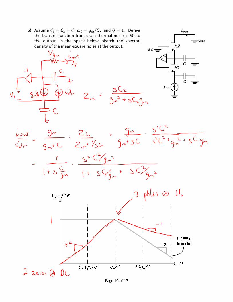
Page 10 of 17
b) Assume , / , and 1 . Derive the transfer function from drain thermal noise in to the output. In the space below, sketch the spectral density of the mean‐square noise at the output.
iin
C-1
ac
ac
iout
C
M1
M2
Initials: ____________
Page 11 of 17
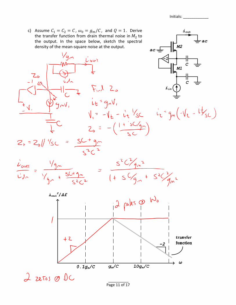
c) Assume , / , and 1 . Derive the transfer function from drain thermal noise in to the output. In the space below, sketch the spectral density of the mean‐square noise at the output.
iin
C-1
ac
ac
iout
C
M1
M2

Page 12 of 17
Problem 4 (22 Points): The following schematic is a non‐inverting amplifier with a gain of / 1 / . Ignore body effect, channel length modulation, and parasitic
capacitances. is a DC current source with infinite output resistance (infinite resistances can sometimes produce infinite gains). a) Draw the low‐frequency small‐signal circuit for the amplifier and derive the transfer
function / . Do not include .
IBIAS
M1
M2
vout
R2
R1
vin
Initials: ____________
Page 13 of 17
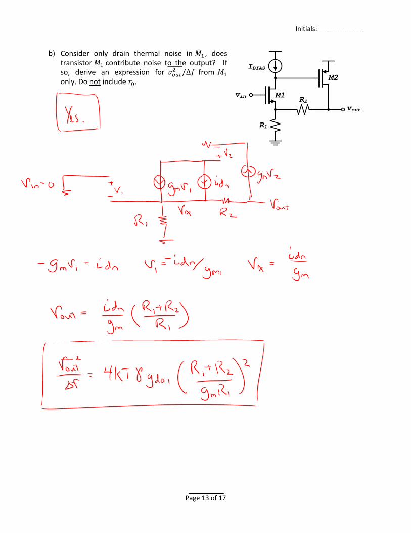
b) Consider only drain thermal noise in , does transistor contribute noise to the output? If so, derive an expression for /∆ from only. Do not include .
IBIAS
M1
M2
vout
R2
R1
vin
Page 14 of 17
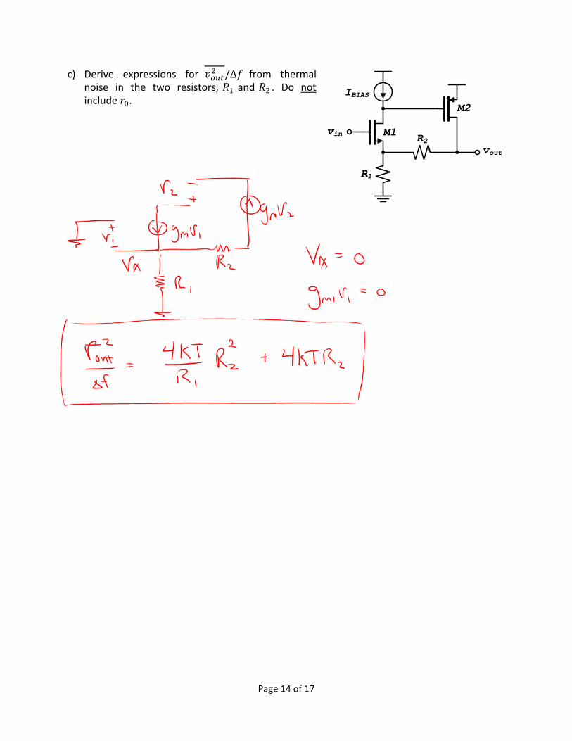
c) Derive expressions for /∆ from thermal noise in the two resistors, and . Do not include .
IBIAS
M1
M2
vout
R2
R1
vin

Initials: ____________
Page 15 of 17
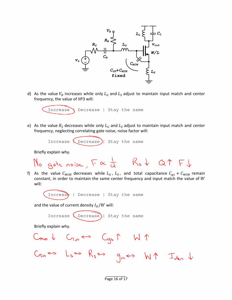
Problem 5 (12 Points): The following parts are multiple choice. Circle only one answer for each part. Refer to the circuit below for all parts. is a DC bias voltage, and and are large values that do not impact the RF performance. a) As the value of is decreased, in order to maintain an input match at the same target
center frequency the value of / will:
Increase | Decrease | Stay the same Briefly explain why. b) As the value increases while keeping fixed, the gain of the amplifier will:
Increase | Decrease | Stay the same Briefly explain why. c) As the value increases while keeping all else fixed, the value of / will:
Increase | Decrease | Stay the same
Briefly explain why.
LG
LS
CMIM
CGS+CMIM
fixed
RS
vs
vout
LL CL
RB
CB
VB
W/L
Page 16 of 17
d) As the value increases while only and adjust to maintain input match and center
frequency, the value of IIP3 will:
Increase | Decrease | Stay the same e) As the value decreases while only and adjust to maintain input match and center
frequency, neglecting correlating gate noise, noise factor will:
Increase | Decrease | Stay the same Briefly explain why. f) As the value decreases while , , and total capacitance remain
constant, in order to maintain the same center frequency and input match the value of will:
Increase | Decrease | Stay the same
and the value of current density / will:
Increase | Decrease | Stay the same Briefly explain why.
LG
LS
CMIM
CGS+CMIM
fixed
RS
vs
vout
LL CL
RB
CB
VB
W/L

Initials: ____________
Page 17 of 17
(Space for additional work)