university of minnesota this is to certify that i have...
TRANSCRIPT

UNIVERSITY OF MINNESOTA
This is to certify that I have examined this copy of a doctoral Dissertation by
Cristinel Ababei
and have found that it is complete and satisfactory in all respects, and that any and all revisions required by the final
examining committee have been made.
_____________________________________________________________ Name of Faculty Adviser
_____________________________________________________________ Signature of Faculty Adviser
_____________________________________________________________ Date
GRADUATE SCHOOL

Design Automation for
Physical Synthesis of VLSI Circuits and FPGAs
A DISSERTATION SUBMITTED TO THE FACULTY OF THE GRADUATE SCHOOL
OF THE UNIVERSITY OF MINNESOTA BY
Cristinel Ababei
IN PARTIAL FULFILLMENT OF THE REQUIREMENTS FOR THE DEGREE OF
DOCTOR OF PHYLOSOPHY
Kia Bazargan
December 2004

© Cristinel Ababei 2004

i
Acknowledgements First of all, I would like to thank my research advisor Prof. Kia Bazargan for his guidance,
positive spirit, and invaluable support throughout the course of my study and work at the
University of Minnesota. He has always been a source of encouragement, and his spirit, ideas,
and personality have been great sources of inspiration.
I would like to thank Prof. George Karypis, Prof. Sachin Sapatnekar, and Prof. Gerald
Sobelman for serving on my Preliminary Oral Examination and dissertation committees and for
their constructive feedback.
During the course of my study at the University of Minnesota, I had the opportunity to meet
and interact with many talented and interesting people from whom I learned many things and
who, in one way or another, contributed to my work and sometimes changed the way I see things
today.
I had a great collaboration with Navaratnasothie Selvakkumaran and Prof. George Karypis. I
admired their hard-work and can-be-done attitude.
I would like to thank Prof. Igor Markov of the University of Michigan for his many prompt
and helpful answers to my questions regarding the Capo placer. Generally, I would like to thank
the EDA community and its researchers, whose many papers that I read shaped my ideas and
research directions.
I was fortunate to be a graduate student at UMN and I will always be fond of Minnesota.
I would like to thank the other members in my group as well as the members of Prof. Sachin
Sapatnekar’s group (VEDA Lab.) for creating an excellent research and social environment. I
would especially like to thank Kartikeyan Bhasyam, Wonjoon Choi, Pongstorn Maidee, and
Hushrav Mogal for many interesting discussions and their collaboration. I would also like to
thank Mahesh Ketkar and Arvind Karandikar my oldest friends and colleagues from the VEDA
Lab. Also, Rupesh Shelar, Venkat Rajappan, Anup Sultania, Jaskirat Singh, Vidyasagar Nookala,
Hongliang Chang, and Brent Goplen have been great people I interacted with.
I thank Radu Marculescu for his constant guidance even when he was far away.

ii
It is hard to voice my thanks and gratitude to my parents for their love and sacrifices
throughout all my schooling endeavors. My siblings Marcel and Angelica never stopped
encouraging me.
There are no words to express my thanks to my wife Anca for her unconditional love and
faith in me. She was my biggest fan and my main source of encouragement and support for all
these years since we first met in Iasi, our college town.
Finally, I would like to acknowledge the financial support provided by the ECE Department
at the University of Minnesota, my advisor Prof. Kia Bazargan, ACM, and IEEE.

iii
To Anca

iv
Abstract
We address the problem of delay optimization for VLSI circuits and FPGAs at the physical
design stage. A new net-based statistical timing-driven partitioning algorithm demonstrates that
circuit delay can be improved while the run-time remains virtually the same and the cutsize
deterioration is insignificant. Because path-based timing-driven partitioning has the advantage
that global information about the structure of the circuit is captured, we also propose multi-
objective partitioning for cutsize and circuit delay minimization. We change the partitioning
process itself by introducing a new objective function that incorporates a truly path-based delay
component for the most critical paths. To avoid semi-critical paths from becoming critical, the
traditional slack-based delay component is also accounted for. The proposed timing-driven
partitioning algorithm is built on top of the hMetis algorithm, which is very efficient. Simulations
results show that important delay improvements can be obtained. Integration of our partitioning
algorithms into a leading-edge placement tool demonstrates the ability of the proposed edge-
weighting and path-based approaches for partitioning to lead to a better circuit performance. We
propose and develop means for changing a standard timing-driven partitioning-based placement
algorithm in order to design more predictable (predictability is to be achieved in the face of
design uncertainties) and robust (high robustness means that performance of the design is less
influenced by noise factors and remains within acceptable limits) circuits without sacrificing
much of performance. A new timing-driven partitioning-based placement and detailed routing
tool for 3D FPGA integration is developed and it is shown that 3D integration results in
significant delay and wire length reduction for FPGA designs.

v
Contents
1 INTRODUCTION 1
1.1 Motivation 1 1.1.1 General Perspective 1 1.1.2 A Closer Look 3
1.2 Research Approach and Contributions 6
1.4 Dissertation Outline 9
2 PRELIMINARIES 11
2.1 Introduction 11
2.2 Partitioning 15
2.3 Standard Cell Placement 17
2.4 Physical Design for FPGAs 20
2.5 Summary 23
3 STATISTICAL TIMING-DRIVEN PARTITIONING AND PLACEMENT 24
3.1 Introduction 24 3.1.1 Motivation 24 3.1.2 Previous Work 25 3.1.3 Research Approach 27
3.2 Statistical Timing Analysis 27
3.3 Statistical Timing-driven Partitioning 31
3.4 Simulation Results 34
3.5 Partitioning-based Placement 35
3.6 Summary 38

vi
4 PATH-BASED TIMING-DRIVEN PARTITIONING AND PLACEMENT 41
4.1 Introduction 41 4.1.1 Motivation 41 4.1.2 Research Approach 42
4.2 Multi-objective hMetis Partitioning: Cutsize and Delay Minimization 43
4.3 Path-based Timing-driven Partitioning 45 4.3.1 Choosing K-most Critical Paths 45 4.3.2 Algorithm Details 49
4.4 Simulation Setup and Results 51 4.4.1 Simulation Setup 51 4.4.2 Simulation Results 51
4.5 Partitioning-based Placement 56
4.6 Summary 58
5 PLACEMENT FOR ROBUSTNESS PREDICTABILITY AND PERFORMANCE 59
5.1 Introduction 59 5.1.1 Motivation 59 5.1.2 Previous Work 60 5.1.3 Research Approach 61
5.2 Predictability Analysis 61
5.3 Robustness Analysis 66
5.4 Case Study: Partitioning-based Placement 70
5.5 Simulation Results 73
5.6 Summary 74
6 PLACE AND ROUTE FOR 3D FPGAS 76
6.1 Introduction 76 6.1.1 Motivation 76 6.1.2 Previous Work 77 6.1.3 Research Approach 79
6.2 Overview of TPR 81

vii
6.3 Placement Algorithm 83 6.3.1 Initial Partitioning and Assignment to layers 83 6.3.2 Placement Method 87
6.4 Routing Algorithm 89 6.4.1 Description of Detailed Routing Algorithm 89 6.4.2 Computation of Total and Foot-print Area 92
6.5 Simulation Results 93 6.5.1 3D Architectures 93 6.5.2 Delay Results of TPR 95 6.5.3 Wire Length Results of TPR 99 6.5.4 Experiments Using Mixed Partitioning- and SA- based Placement Algorithm 103
6.6 Summary 106
7 CONCLUSIONS AND FUTURE WORK 107
7.1 Dissertation Summary 107
7.2 Future Work 108 7.2.1 Multi-objective Optimization 108 7.2.2 Robust Design under Uncertainty 109 7.2.3 Architectural Studies and Efficient CAD Support for 2D and 3D FPGAs 110
BIBLIOGRAPHY 111
STATISTICAL TIMING ANALYSIS 122
DELAY MODEL 128

viii
List of Tables Table 1 Partitioning simulation results. Delay is computed using static timing analysis. 14 Table 2 Placement simulation results. Delay is computed using static timing analysis. Simulations were
performed on the same machine as those in Section 3.4. 16 Table 3 Comparison between our methods and pure hMetis. 37 Table 4 Timing driven partitioning placement vs. min-cut driven partitioning placement. 56 Table 5 Comparison of the proposed placement algorithm to the classic net-based timing-driven
partitioning-based placement. Delay is the delay reported by a static timing analysis algorithm and Standard deviation is the standard deviation of the overall circuit delay after placement (the smaller it is the more predictable is the circuit). Delay-change is the change in static delay after the placement is changed in scenarios 1 or 2 (smaller means circuit more robust). 40
Table 6 Simulated circuits: statistics, vertical channel width (VCW) for successful routing, and run-time (TPR compiled with g++ on a Linux box running on a Xeon 2.54GHz with 2G of memory). 104
Table 7 Average (of all circuits) of Delay, wire-length (WL), horizontal channel width (HCW), and routing area after successful routing for Sing-Seg architecture. 105
Table 8 Average (of all circuits) of Delay, wire-length (WL), horizontal channel width (HCW), and routing area after successful routing for Multi-Seg architecture. 105

ix
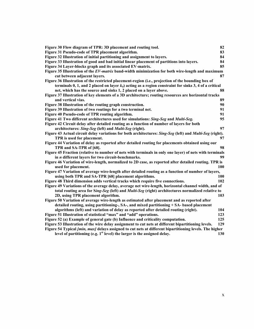
List of Figures Figure 1 Variation of chip capacity and designer productivity give rise to the productivity gap
(source: NTRS97). 2 Figure 2 Interconnect delay dominance as technology advances (source ITRS 2002). 3 Figure 3 Schematic diagram of a typical design process. 4 Figure 4 Y chart also known as Gajsky’s Y chart [41]. 12 Figure 5 Typical design flow. 13 Figure 6 Steps during a typical PD cycle. 14 Figure 7 Diagram depicting design styles. 17 Figure 8 Illustration of standard cell placement. 18 Figure 9 Design styles comparison. 20 Figure 10 (a) Typical symmetric array FPGA (b) Subset switch block. 21 Figure 11 (a) Illustration of controlling pass transistors and multiplexers (b) Three-input LUT. 22 Figure 12 (a) Circuit example (b) Placement on symmetric array FPGA. 23 Figure 13 A sample circuit. 29 Figure 14 (a) Associated DAG with shown criticalities; the most critical hyperedge 8, 9, 10 is cut by
Partitioning 1 (b) Partitioning 2 does not cut the most critical hyperedge; therefore, circuit delay is smaller. 29
Figure 15 Voltage at the output of G6 (vertex 11 in Figure 14.b). 31 Figure 16 (a) Schematic diagram of the proposed algorithm (b) Recursive bipartitioning tree, which
illustrates bipartitioning levels. 32 Figure 17 Statistical timing-driven partitioning. 33 Figure 18 Simulation setup. 35 Figure 19 Example of a situation when net-based partitioning approaches fail to differentiate
partitionings with the same cutsize but different delays. 42 Figure 20 The path delay distribution for too_large (total number of paths is 14781) before and after
partitioning, which is done with and without updating the most critical paths in region 1 (0.9, 1]. 47
Figure 21 Path delay distribution when K most critical paths are updated or not illustrates the delay improvement obtained when K most critical paths are updated for too_large. 49
Figure 22 Simulation setup for comparison of our proposed multi-objective hMetis partitioning algorithm to pure hMetis algorithm. 51
Figure 23 Delay results comparison. 55 Figure 24 Cutsize results comparison. 55 Figure 25 (a) Standard deviation at the output σout of a series of m delay elements (b) Standard
deviation at the output of a gate with m inputs 63 Figure 26 Study cases. 64 Figure 27 Standard deviation when one delay element increases and another decreases for a) a series
of delay elements and b) delay elements as LATs gate inputs. The x axis represents the varying length l2 and the y axis is the ratio between the sum of means of fixed elements over the sum of varying means. Default standard deviation of all delay elements is 10% (top) or 25% (bottom). 66
Figure 28 (a) Average output delay of a three-input gate with input LAT range of 0, 0.5, and 1 (b) Average cell delay for the combination of the control factor with the noise factor. 69
Figure 29 (a) Standard deviation of LATs at nodes on critical path for too_large for 25% and 5% standard deviation for wire and gate (b) Enlarged bottom-left corner of Figure 25.b. 72
x
Figure 30 Flow diagram of TPR: 3D placement and routing tool. 82 Figure 31 Pseudo-code of TPR placement algorithm. 83 Figure 32 Illustration of initial partitioning and assignment to layers. 84 Figure 33 Illustration of good and bad initial linear placement of partitions into layers. 84 Figure 34 Layer-blocks graph and its associated EV-matrix. 85 Figure 35 Illustration of the EV-matrix band-width minimization for both wire-length and maximum
cut between adjacent layers. 87 Figure 36 Illustration of the restricted placement-region (i.e., projection of the bounding box of
terminals 0, 1, and 2 placed on layer k0) acting as a region constraint for sinks 3, 4 of a critical net, which has the source and sinks 1, 2 placed on a layer above. 88
Figure 37 Illustration of key elements of a 3D architecture; routing resources are horizontal tracks and vertical vias. 89
Figure 38 Illustration of the routing graph construction. 90 Figure 39 Illustration of two routings for a two terminal net. 91 Figure 40 Pseudo-code of TPR routing algorithm. 91 Figure 41 Two different architectures used for simulations: Sing-Seg and Multi-Seg. 95 Figure 42 Circuit delay after detailed routing as a function of number of layers for both
architectures: Sing-Seg (left) and Multi-Seg (right). 97 Figure 43 Actual circuit delay variations for both architectures: Sing-Seg (left) and Multi-Seg (right).
TPR is used for placement. 97 Figure 44 Variation of delay as reported after detailed routing for placements obtained using our
TPR and SA-TPR of [68]. 98 Figure 45 Fraction (relative to number of nets with terminals in only one layer) of nets with terminals
in n different layers for two circuit-benchmarks. 99 Figure 46 Variation of wire-length, normalized to 2D case, as reported after detailed routing. TPR is
used for placement. 100 Figure 47 Variation of average wire-length after detailed routing as a function of number of layers,
using both TPR and SA-TPR [68] placement algorithms. 100 Figure 48 Third dimension adds vertical tracks which require five connections. 102 Figure 49 Variations of the average delay, average net wire-length, horizontal channel width, and of
total routing area for Sing-Seg (left) and Multi-Seg (right) architectures normalized relative to 2D, using TPR placement algorithm. 103
Figure 50 Variation of average wire-length as estimated after placement and as reported after detailed routing, using partitioning-, SA-, and mixed partitioning + SA- based placement algorithms (left) and variation of delay as reported after detailed routing (right). 104
Figure 51 Illustration of statistical “max” and “add” operations. 123 Figure 52 (a) Example of general gate (b) Influence and criticality computation. 125 Figure 53 Illustration of the wire delay assignment to cut nets at different bipartitioning levels. 129 Figure 54 Typical [min, max] delays assigned to cut nets at different bipartitioning levels. The higher
level of partitioning (e.g. 1st level) the larger is the assigned delay. 130

1 Introduction
1
1 Introduction
1.1 Motivation
1.1.1 General Perspective
The continuous advance – at exponential pace – of technology for more than three decades
facilitated the implementation of very complex and fast designs. This progress has followed
Moore’s law (which says that the number of transistors on a chip doubles roughly every two
years) with incredible accuracy. For example, currently, Intel's fastest Pentium 4 chip clocks in at
3.2 GHz and has about 55 million transistors whereas chips containing 1 billion transistors –
could be running at 10 GHz – will hit the market in 2007. However this progress has come at a
cost and has been accompanied by unexpected difficulties, emerged due to miniaturization. One
such difficulty is the productivity gap, depicted in Figure 1, which is a result of the faster increase
of circuit complexities compared to the increase in designer productivity; the latter mainly taking
place due to improved, more efficient CAD tools and bigger computational power. This problem
is far from being solved and today fewer and fewer companies can close this gap, and when that
happens, larger and larger design, test, verification and manufacturing teams are required.
1 Introduction
2
1998
21%/Yr. Productivity growth rate
58%/Yr. Complexity growth rate
1
10
100
1,000
10,000
100,000
1,000,000
10,000,000
10
100
1,000
10,000
100,000
1,000,000
10,000,000
100,000,000Lo
gic
Tran
sist
ors/
Chi
p (K
)
Tran
sist
or/S
taff-
Mon
th
xxxxxx
x x
2003
Figure 1 Variation of chip capacity and designer productivity give rise to the productivity gap (source:
NTRS97).
Furthermore, due to the non-uniform scaling of transistors and interconnects, previously
ignored perturbations – such as process variations, temperature, and supply voltage changes –
have become major design challenges because of their significant negative impact on the
predictability of classic design methodologies, as well as on performance. New design techniques
and CAD support, which shall lead to more robust designs and more predictable design
methodologies, is needed.
Moreover, due to the continuously increased chip sizes and transistor scaling, interconnect
delay has become the dominant factor in determining circuit speed as illustrated in Figure 2. This
problem can be partially alleviated using buffer insertion or pipelining techniques but is also far
from being solved.

1 Introduction
3
0.5 0.4 0.3 0.2 0.1 0.08 0.06
0
5
10
15ITRS 2002
interconnect Delay
gate Delay
Del
ay [p
s]
Generation [µm]
Figure 2 Interconnect delay dominance as technology advances (source ITRS 2002).
1.1.2 A Closer Look
A typical design flow model is shown in Figure 3. The process of going from design specification
to silicon implementation can be viewed as one of successive refinement, from the initial
specification and register-transfer level (RTL) implementation to a logic level representation, via
high level logic synthesis, followed by physical synthesis and design verification. This refinement
is an entire collection of various optimization techniques, which pursue specific objectives, such
as minimizing circuit delay (i.e., improving performance), power consumption or chip area or
improving design reliability, as well as predictability.
After the last stage, if the design objectives are met, the design can be manufactured (i.e.,
fabricated in silicon). Nevertheless, if the design objectives (performance being the most
important most often) are not met, the design process has to loop back to previous stages, and try
to correct the problem, by either re-implementing parts of the design or re-optimizing it. In this

1 Introduction
4
way, depending on the stage the design process loops back to, a number of design steps have to
be repeated, with no guarantee of meeting the design objectives. If the problem to be corrected is
small, then the design process will loop back to one of the back-end design stages, such as
placement or routing. At later design stages, the design detail increases and more information
about the final circuit structure and more accurate modeling techniques are available, which
makes the evaluation of different cost functions more reliable and the whole design methodology
more predictable. However, the impact of various optimization decisions at later design stages is
smaller compared to the impact, which decisions made at higher levels can have. Therefore when
the design objectives are not met by a big margin the design process will loop back to early,
front-end, design stages.
Figure 3 Schematic diagram of a typical design process.
High Level Design Specification(e.g., VHDL, Verilog)
High Level Synthesis (Technology Independent Optimization,
Technology Mapping)
Simulation / VerificationTest Generation
Layout Synthesis (Partitioning, Floorplaning, Placement, Global
and Detailed Routing, Transistor Sizing)
Verification
Manufacturing (Tape Out)
Tim
ing
clos
ure
Increasing design detail

1 Introduction
5
This design cycle is expensive, and can lead to significant delays in the time to market of a
product. With such a scenario, it is obvious that the methodology described in Figure 3 is
problematic. The designer needs to know how well the design is going to perform in its final
form, but for that, information from later stages of the design process is needed. At early design
stages the information about the final design is vague and therefore predictions on how the final
design will perform are inaccurate. The impact of optimization decisions can have drastically
different consequences at later stages. These consequences are not apparent when the choices are
made, and at later stages, when the consequences are apparent, it is too expensive to go back and
change the initial decision. The uncertainty introduced by variations due to process variations and
temperature/voltage changes does only worsen the entire design process. Relying only on
optimization approaches that consider only the gate delay is not desirable because in current
technologies the wire delay is dominant, accounting for more than 70% of the total circuit delay
[75]. One way to solve this dilemma is to try to elevate more information about the final design to
the level of early design stages. This can be done by either adopting new design methodologies,
such as platform-based design [87], or, as we propose in this thesis, by improving the estimation
of various design metrics and integrating them into efficient algorithms, which shall be better
aware of the later stages and the final implementation. Because of the continuously increasing
circuit sizes, most of the wire delay is due to global interconnects (i.e., spanning multiple
modules). A possible solution to this problem is to adopt 3D integration. 3D integration could
significantly reduce wire-lengths, boost yield, and could particularly be useful for FPGA fabrics
because it could address problems related to routing congestion, limited I/O connections, and

1 Introduction
6
long wire delays. Practical application of 3D integrated circuits yet needs to gain momentum,
partly due to a lack of efficient 3D CAD tools.
The research presented in this dissertation is aimed directly at the problems discussed so far.
We develop (1) improved partitioning algorithms that can be embedded in partitioning based
placement tools (divide and conquer approach suitable for the increasing circuit sizes) which lead
to improvements in circuit delay, (2) an analysis methodology to better understand the
relationship between robustness, predictability and performance of VLSI circuits and techniques
to gear a standard timing-driven partitioning-based placement algorithm to design more
predictable and robust circuits without sacrificing much of performance, (3) a placement and
detailed routing tool for 3D FPGAs, which is used to explore potential benefits in terms of
performance and area that future 3D integration technologies can achieve.
1.2 Research Approach and Contributions
The increase in circuit complexities and the high demand for short time-to-market products
force designers to adopt divide-and-conquer and platform-based design methodologies.
Furthermore, ever-growing performance expectations require designers to perform optimization
at all levels of the design cycle. Significant contribution of interconnect to the area and delay of
today’s and future chips, combined with the fact that partitioning and placement have a great
impact on the interconnect distribution, makes partitioning and placement very important steps
during physical design. It is imperative to account for timing during these design steps to allow
for early wire planning. In the first part of this dissertation, we address the problem of delay
optimization at the physical design stage. A new net-based statistical timing-driven partitioning
algorithm demonstrates that circuit delay can be improved while the run-time remains virtually

1 Introduction
7
the same and the cutsize deterioration is insignificant [3]. Path-based timing-driven partitioning
has the advantage that global information about the structure of the circuit is captured. We
propose multi-objective partitioning for cutsize and circuit delay minimization [1], [2]. We
change the partitioning process itself by introducing a new objective function that incorporates a
truly path-based delay component for the most critical paths. To avoid non-critical paths from
becoming critical, the traditional slack-based delay component is also accounted for. The
proposed timing-driven partitioning algorithm is built on top of the hMetis algorithm, which is
very efficient. Integration of our partitioning algorithms into a leading-edge placement tool
demonstrates the ability of the proposed edge-weighting and path-based approaches for
partitioning to lead to a better circuit performance.
A design methodology should offer predictable and robust designs at the best performance.
High robustness means that performance of the design is less influenced by noise factors and
remains within acceptable limits. The design methodology should also be predictable.
Predictability is to be achieved in the face of design uncertainties, which are caused by either
incomplete system specification or inherent difficulty of estimating performance metrics during
the optimization process. In the second part of this dissertation we analyze the relationship
between robustness, predictability and performance (optimality) and seek means for their control.
We apply our techniques to timing-driven partitioning-based placement algorithm in order to
design more predictable and robust circuits without sacrificing much of performance [4]. We
regard the optimization process under uncertainty as the iterative computation of a number of
objective functions, which depend on variables whose values are known within a range of values
(i.e., as probability distributions or as intervals within which these variables lie). In this context,
predictable design means the ability to accurately compute the objective function (within the

1 Introduction
8
chosen modeling framework), and to find means of making current estimations closer to the real
final values. We use the standard deviation as the measure of predictability of the overall circuit
delay distribution at the primary outputs, as well as at the output of each cell inside the circuit.
This means that the smaller the standard deviation, the more predictable is the delay. The slope of
the variation of the standard deviation of the overall circuit delay, when gate and wire delays
change, characterizes the robustness of the circuit.
The potential impact of practical application of 3D integration for FPGAs is currently unclear
partly due to a lack of efficient 3D CAD tools. In the third part of this dissertation our goal is to
present an efficient placement and detailed routing tool for 3D FPGAs. Unlike previous works on
3D FPGA architecture and CAD tools, we investigate the effect of 3D integration on delay, in
addition to wire-length because wire-length alone cannot be relied on as a metric for 3D
integration benefits. Apart from the commonly used single-segment architecture, we also study
multi-segment architectures in the third dimension. Our placement algorithm is partitioning-
based, and hence scalable with the design size. We show that 3D integration can result in smaller
circuit delay and wire-length.
The research presented in this dissertation can be seen as only the beginning of longer term
endeavors with future directions discussed in the last chapter. Nevertheless, it still has produced
some worthwhile results, which can be summarized as main contributions as follows:
• New timing-driven partitioning algorithms: The use of statistical timing criticality
concept to change the partitioning process itself (classified as a net-based partitioning
approach), on one hand, and the use of a new objective function that incorporates a truly
path-based delay component for the most critical paths (classified as path-based

1 Introduction
9
approach), on the other hand, proved to lead to performance improvement at both
partitioning and placement level.
• Better understanding of the relation between robustness, predictability, and
performance: At the partitioning and placement levels of abstraction we have built a
modeling framework, which allowed us to explore for the first time ways of performing
physical design to achieve more predictable and robust circuits without sacrificing
much of performance.
• TPR (Three-dimensional Place and Route): We have developed a partitioning-based
placement and detailed routing toolset. We have used it as a platform in performing
architectural analysis in order to analyze potential benefits that 3D integration can
provide for FPGAs. More specifically, we have placed and detailed routed circuits onto
3D FPGA architectures and studied the variation in wire-length and, for the first time, in
total circuit delay compared to their 2D counterparts. Our results can guide researchers in
designing high performance 3D FPGA fabric architectures.
1.4 Dissertation Outline
This dissertation is organized as follows. Chapter 2 is a general overview of physical design
(PD) of VLSI circuits and FPGAs. It builds the background for the topics presented in the rest of
this dissertation. The first part, encompassing Chapters 3 and 4, presents new partitioning
algorithms (net based and path based) that can lead to circuit delay improvements both at the
partitioning abstraction level and after they are embedded into a placement algorithm. The second
part of this dissertation, spanning Chapter 5, investigates the relation between robustness,
predictability, and performance. Chapter 6, which represents the third part of the dissertation, is

1 Introduction
10
concerned with the presentation of a new placement and detailed routing tool used for exploration
of 3D technologies. Conclusion and future research directions are presented in Chapter 7.
Appendix A represents a detailed presentation of statistical timing analysis, which is used to build
the modeling framework for the research in Chapter 3 and Appendix B discusses our delay
modeling.

1 Introduction
11
2 Preliminaries
2.1 Introduction
This chapter is devoted to the presentation of physical design of VLSI circuits and FPGAs. The
abbreviation VLSI stands for Very Large Scale Integration, which refers to integrated circuits that
have more than 105 transistors. FPGA stands for Field Programmable Logic Arrays, which is a
different design style described later in this chapter. We will present a rather general view of the
basic design steps in a typical physical design phase in order to build the background for the
topics presented in the rest of this dissertation.
In dealing with the ever increasing complexity of integrated circuits the concepts of hierarchy
and abstraction are helpful [41]. Hierarchy captures and shows the structure of a design at
different levels of description whereas abstraction hides the lower level details. Abstraction
makes it possible to reason about a limited number of interacting parts at each level in the
hierarchy. Each part is, at its turn, composed of interacting subparts at a lower level of
abstraction. This decomposition continues till the basic building blocks (e.g., transistors) of a
VLSI circuits are reached. Because a single hierarchy is not enough to properly describe the VLSI
process, there is a general consensus to define three design domains, each with its own hierarchy
(see Figure 4). These domains are as follows [41]:
• The behavioral domain. The design or part of it is seen a black box and the relations
between inputs and outputs are given with no reference to their implementations. For

1 Introduction
12
example, a design with the complexity of a several transistors can be described using
Boolean algebra equations or truth tables. At even higher levels of abstraction a design
can be represented as interacting algorithms that will realize the computation described
with no visible connection to hardware.
• The structural domain. The circuit is seen as the composition of subcircuits. A design
description in this domain captures information on the subcircuits and their connectivity.
For example, a schematic showing how gates are interconnected to implement some
arithmetic unit represents a structural description at the gate abstraction level in this
domain.
• The physical (or layout) domain. Descriptions in this domain give information on how
the subparts that can be seen in the structural domain, are located on two (usually)
dimensional plane. For example a cell that may represent the layout of a logic gate will
consist of mask patterns which form the transistors of this gate and its interconnections.
system synthesis STRUCTURAL domain
Processors, memories, busses
Transistor layout
PHYSICAL domain
Cells
Modules
Floorplans, chips Physical partitions, boards
BEHAVIORAL domain
Transistors
Gates, FFs Registers, ALUs
PC
Transfer functions
Boolean expressions Register transfers
Flowcharts, Algorithms
Systems register-transfer synthesis
logic synthesis
circuit synthesis
Figure 4 Y chart also known as Gajsky’s Y chart [41].

1 Introduction
13
Apart from describing the three design domains in one picture, the Y-chart is a very powerful tool
to illustrate different design methodologies. For example, a typical top-down design methodology
(further illustrated in Figure 6) is described by an inward spiral path in Figure 4. Parts of the
design with known behavior are decomposed into smaller blocks with simpler behavior and an
interconnection structure. This corresponds with a transition from the behavioral to the structural
domain. A transition step from the structural to the physical domain follows and this illustrates
the fact that layout is taken into account during all design stages. Then, each subpart can be
thought to be located on the behavioral axis and is decomposed at its turn. This inward spiral path
continues until the circuit has been specified down to the lowest structural level (i.e., transistors).
Design specification
Functional / architecture
design
RTL and logic synthesis
module fz(a,b,c,d); input a,b,c,d; output z; assign z = ((a or b)and(c or d)); endmodule
Behavior representation HDL representation
a b c d
z
Gate-level representation
a b
c d z
Pull-up
Vdd
Vss Switch-level representation
Physical synthesis
Fabrication
Packaging
Circuit design
Extraction verification
GDSII
THIS DISSERTATION
Figure 5 Typical design flow.
Specification is a description of what the system does. During the design process the structure
of the system is determined, using different methods to achieve a function and logical structures

1 Introduction
14
that perform the architecture. Realization (fabrication) materializes the physical structures in a
certain technology (e.g., CMOS) using a design style (described shortly). Physical design
basically converts a circuit description (resulted from logic synthesis) into a geometric description
(GDSII file), which is used to manufacture a chip. A typical physical design cycle has the
following steps (see Figure 6):
• Logic partitioning
• Floorplanning, placement, and pin assignment
• Routing (global and detailed)
• Compaction
• RLC extraction & verification
PHYSICAL DESIGN
Circuit design
Cut 2
Cut 1
Floorplanning Placement
Routing
Compaction
Partitioning
Extraction Verification
Fabrication
Figure 6 Steps during a typical PD cycle.
The main two steps of a typical PD flow are placement and routing. Partitioning can be used
to first divide the circuit into smaller sub-circuits which can be optimized individually. Individual

1 Introduction
15
solutions are put together to give the solution of the entire larger circuit. In this chapter we will
first discuss partitioning and outline its role in PD for VLSI. We will then describe the placement
problem mainly for standard cell as well as for FPGAs.
2.2 Partitioning
Generally, partitioning is the decomposition of a complex system into smaller subsystems until
each subsystem has manageable size. More formally, the partitioning process takes as input a
graph or hypergraph, possibly with vertex (node) and/or edge (arc) weights and the objective is to
assign nodes to partitions such that the cutsize (cutset) is minimized subject to constraints such as
number of partitions (K-way partitioning) or maximum capacity of each partition, or maximum
allowable difference between partitions.
Graph partitioning arises as a preprocessing step to divide-and-conquer algorithms, where it
is often a good idea to break things into roughly equal-sized pieces. Several different flavors of
graph partitioning arise depending on the desired objective function [79]:
• Minimum cutset - The smallest set of edges to cut that will disconnect a graph can be
efficiently found using network flow methods. Since the smallest cutset can split off only
a single vertex, the resulting partition might be very unbalanced.
• Graph partition - A better partition criterion seeks a small cut that partitions the vertices
into roughly equal-sized pieces. This problem is NP-complete [40] and many heuristics
have been proposed, which work well in practice.
• Maximum cut - Given an electronic circuit specified by a graph, the maximum cut
defines the largest amount of data communication that can simultaneously take place in
the circuit. The highest-speed communications channel should thus span the vertex

1 Introduction
16
partition defined by the maximum edge cut. Finding the maximum cut in a graph is NP-
complete [36], [40].
The basic approach to dealing with graph partitioning or max-cut problems is to construct an
initial partition of the vertices (either randomly or according to some problem-specific strategy)
and then sweep through the vertices, deciding whether the size of the cut would increase or
decrease if we moved this vertex over to the other side. The decision to move v can be made in
time proportional to its degree by simply counting whether more of neighbors of v are on the
same team as v or not. Of course, the desirable side for v will change if many of its neighbors
jump, so multiple passes are likely to be needed before the process converges on a local optimum.
Even such a local optimum can be arbitrarily far away from the global max-cut.
One of the most notable heuristics is the Kernighan-Lin (KL) algorithm [57] which was later
improved by the Fiduccia-Mattheyses (FM) algorithm [39]. The KL algorithm is an iterative
improvement technique and works on non-weighted graphs. It iterates as long as the cutsize
improves: (i) Find a pair of vertices that result in the largest decrease in cutsize if exchanged, (ii)
Exchange the two vertices (potential move), (iii) “Lock” the vertices, (iv) If no improvement
possible, and still some vertices unlocked, then exchange vertices that result in smallest increase
in cutsize. Its main drawbacks are: it finds balanced partitions only, it does not use weights for the
vertices, it has high time complexity, it work only on edges, not hyper-edges.
The FM algorithm is a modified version of KL to mainly improve on the run-time. Among its
main advantages is that it works with unbalanced partitions, introduces special data structure to
improve time complexity, vertices can have weights, the concept of cutsize is extended to
hypergraphs, and it can be extended to multi-way partitioning. Other partitioning algorithms
include min-cut/max-flow, Ford-Fulkerson (for unconstrained partitions), ratio cut, genetic
1 Introduction
17
algorithm, and simulated annealing. To cope with the increased size of graphs, multi-level
approaches have been proposed [56], [30], [13].
Within the context of PD for VLSI, partitioning is used to divide the circuit (represented as a
graph) into sub-circuits (sub-graphs) of smaller size, which can be handled easier individually.
Most often, partitioning is closely connected to the placement process. Placement can be done by
recursive bipartitioning or quadrisection (see next chapters) with local refinement techniques,
which use usually simulated annealing. Analytic placers such as Gordian [58] also use
partitioning to assign nodes to different chip regions in order to partially remove overlaps and
help convergence to a stable solution. The traditional objective of partitioning used to be the
cutsize. However, in the context of design automation for VLSI, the cost function of the
partitioning process need be augmented with delay components. This means that delay is
optimized early during the design cycle where optimization decisions can be made easier and can
lead to a better wire-planning, which eventually can reduce the design cycles. Ways of including
delay into the partitioning optimization process will be described in the next two chapters.
2.3 Standard Cell Placement
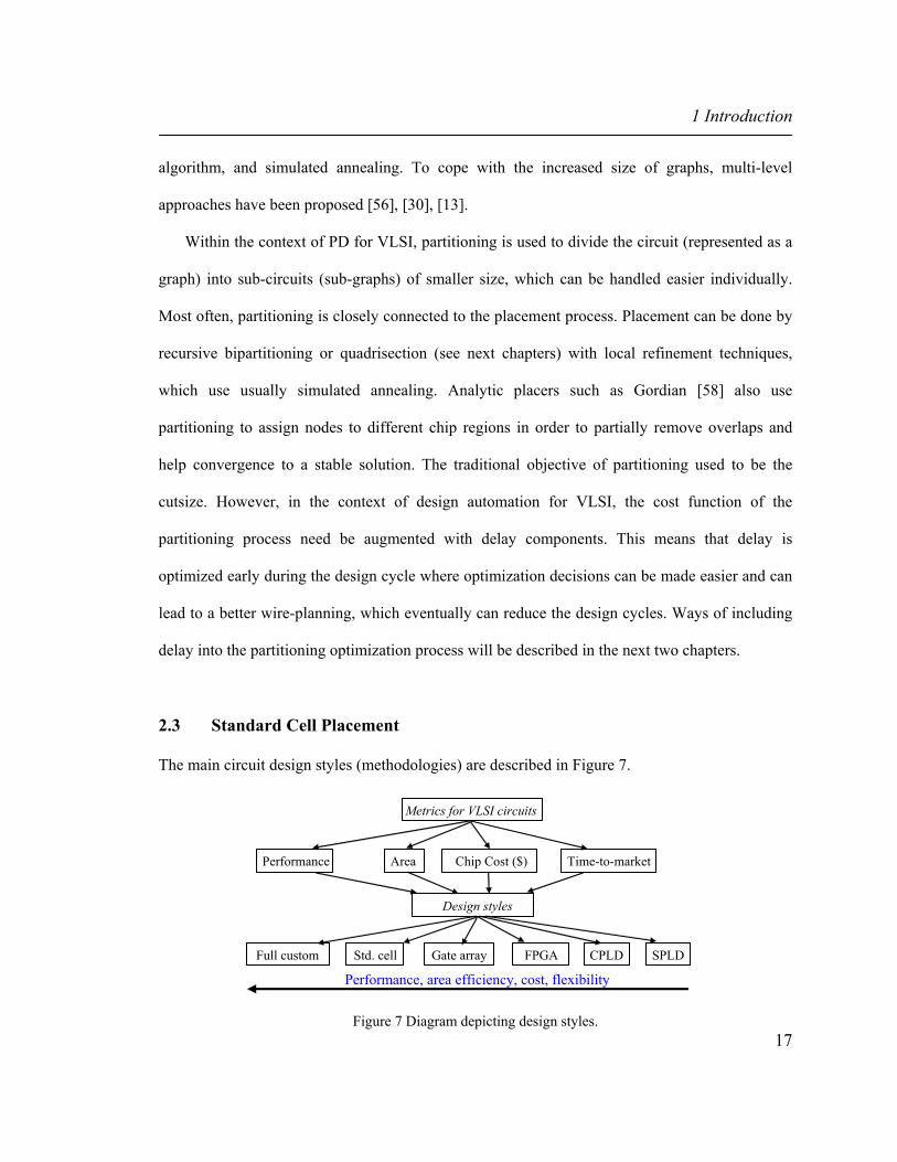
The main circuit design styles (methodologies) are described in Figure 7.
Metrics for VLSI circuits
Performance, area efficiency, cost, flexibility
Performance Area Chip Cost ($) Time-to-market
Design styles
Full custom Std. cell Gate array CPLD FPGA SPLD
Figure 7 Diagram depicting design styles.

1 Introduction
18
The full custom approach uses hand-crafted functional and physical blocks. Because the
number of such blocks is relatively small the placement problem size is rather relatively small
and becomes a floorplanning problem (macro-cell placement). The efforts and costs of this design
style are high and therefore high quality and high production volume are expected. The standard
cell design methodology uses cells (such as OR, NAND, XOR, etc.), which are characterized and
stored in libraries. The placement of cells on the chip area is performed on rows. Cell rows are
spaced to leave extra room for routing, which is usually done using up to eight-nine metal layers.
An example of a standard cell placement is shown in Figure 8. These cells however need be
updated when technology changes. The main advantage is that it is easy to develop CAD tools for
design and optimization. Because the level of abstraction is relatively low, the placement problem
size is large. Also, tremendous characterization effort (e.g., parameterized area and delay over
ranges of temperatures and operating voltage) is needed.
C A B D
BBD
CA DCA
Figure 8 Illustration of standard cell placement.
Apart from standard cells there can also be macro-cells (PLA, ALU, etc.) which need be
placed. In this case the placement is called mixed standard cell and macro-cell placement. The

1 Introduction
19
main optimization objective of standard cell placement algorithms used to be the total wire-
length. The total wire-length represents the sum of lengths of each net in the circuit. At the
placement level (when the exact routing of each net is not known yet) the wirelength of each net
is commonly approximated by the half perimeter of the bounding box of all terminals of a net.
However, due to the fact that with the advance of technology into deep submicron geometries,
interconnects have become the dominant factor for the performance (delay) of a circuit. This
leads to an increased importance of the placement design step where wire planning and
performance optimization are treated as direct optimization goals because relying on wirelength
optimization only may not be enough (a minimum total wire-length does not necessarily mean
best circuit delay). The main standard cell placement approaches are as follows. (a) Constructive
placement techniques are based on the idea of divide-and-conquer. They usually use
bipartitioning or quadrisection to divide the problem into smaller problems, which can then be
placed individually with a better placement technique such as branch-and-bound or simulated
annealing. These approaches can be top-down when partitioning is used, or bottom-up when
clustering is used to divide the problem into smaller, easier to handle, subproblems. This
placement approach has the advantage of being scalable with the ever increasing circuit sizes
while offering competitive solution quality. Most of the ideas presented in following chapters
adopt this placement approach. (b) Iterative methods usually are based on simulated annealing or
force directed technique. They start with an initial placement and iteratively improve the wire-
length and area. (c) Analytic placement algorithms formulate the placement as a constrained
optimization problem where the objective is to minimize usually a quadratic in distance cost
function. Well established quadratic solvers are employed to seek the numerical solution. The
solution has overlapping cells which need be removed during a post processing step. Force-

1 Introduction
20
directed placement algorithms seek placement solutions by searching cell locations with the best
balance between attracting and repelling forces.
Gate array design style uses arrays which are pre-manufactured. Metal and contact layers are
used to programm the chip. It has the advantage that fewer manufacturing steps correlate to lower
fabrication time and cost. The CPLD/FPGA design style is described in the next section.
Programmable logic devices (PLD) design style. Any logic function is implemented using two
level logic embedded into two pre-fabricated arrays of AND and OR gates. A comparison
between all the above design styles is presented in Figure 9.
Full custom Standard cell Gate array FPGA SPLD Density Very high High High Medium Low Performance Very high High High Medium Low Flexibility Very high High Medium Low Low Design time Very long Short Short Very short Very short Manufacturing time
Medium Medium Short Very short Very short
Unit cost – small quantity
Very high High High Low Very low
Unit cost – large quantity
Low Low Low High Very high
Figure 9 Design styles comparison.
2.4 Physical Design for FPGAs
FPGAs are arrays of programmable modules with the capability of implementing any generic
logic function. Wires (routing segments) can be connected by programmable connections inside
switch blocks (SBs) and connection blocks (CBs). A typical (Xilinx XC4000 like) FPGA array is
shown in Figure 10.
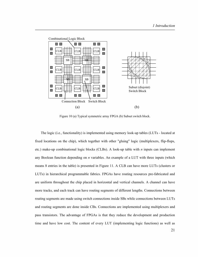
1 Introduction
21
(a) (b)
CLB
CLB
CLB
CLB
CLB
CLB
CLB
CLB
CLB
SB SB
SB SB
Switch Block Connection Block
Combinational Logic Block
Subset (disjoint) Switch Block
Figure 10 (a) Typical symmetric array FPGA (b) Subset switch block.
The logic (i.e., functionality) is implemented using memory look-up tables (LUTs - located at
fixed locations on the chip), which together with other "gluing" logic (multiplexers, flip-flops,
etc.) make-up combinational logic blocks (CLBs). A look-up table with n inputs can implement
any Boolean function depending on n variables. An example of a LUT with three inputs (which
means 8 entries in the table) is presented in Figure 11. A CLB can have more LUTs (clusters or
LUTs) in hierarchical programmable fabrics. FPGAs have routing resources pre-fabricated and
are uniform throughout the chip placed in horizontal and vertical channels. A channel can have
more tracks, and each track can have routing segments of different lengths. Connections between
routing segments are made using switch connections inside SBs while connections between LUTs
and routing segments are done inside CBs. Connections are implemented using multiplexers and
pass transistors. The advantage of FPGAs is that they reduce the development and production
time and have low cost. The content of every LUT (implementing logic functions) as well as

1 Introduction
22
information about what connections are on and off inside SB's and CB's is decided through a
bitstream (loaded from a PROM after power on), which is loaded onto the FPGA. Part of this
bitstream is the content of the LUTs themselves. The rest of it represents information which will
be stored in SRAM cells, which control multiplexers and pass transistors (see Figure 11).
(b)
M G
S D
M
0
S 1
MUX
(a)
a
M M M M M M M M
b
c
z = f(a, b, c)
Figure 11 (a) Illustration of controlling pass transistors and multiplexers (b) Three-input LUT.
The placement and routing of a circuit implemented on FPGAs is essentially similar to the
case of standard cell design style (see Figure 12). The main objective is usually the performance
of the circuit. However performance (i.e., delay) is not directly proportional to the Manhattan
distance as in the case of standard cell placement. Instead, the dominant factor is the number of
routing segments used to route a net. Using more routing segments (i.e., more switch connections
along the route) increases the delay because switches have large delays. Our goal, at placement
level, is to place all the cells (which now are functions embedded into LUTs) such that the final
wirelength and delay will be minimized and the circuit will be fully routable using a minimum
number of routing tracks (which eventually will translate into minimum chip area) because in
practice, pre-fabricated FPGA chips have limited routing resources.

1 Introduction
23
(a) (b) Figure 12 (a) Circuit example (b) Placement on symmetric array FPGA.
2.5 Summary
This chapter discussed physical synthesis as one of the main design steps in a typical design flow.
Emphasis was put on presenting graph partitioning within the context of design automation for
VLSI circuits. Placement for both VLSI circuits and FPGAs was presented as well. We thus built
the basic theoretical framework for presenting our contributions in the next chapters.

3 Statistical Timing-driven Partitioning and Placement
24
3 Statistical Timing-driven
Partitioning and Placement
In this chapter, we present a method for statistical timing driven hMetis-based partitioning. We
approach timing driven partitioning from a new perspective, compared to previous works: we use
a statistical timing criticality concept to change the partitioning process itself. We exploit the
hyperedge coarsening scheme of the hMetis partitioner for our timing minimization purpose. This
allows us to perform partitioning such that the most critical nets in the circuit are not cut and
therefore timing minimization can be achieved. The use of the hMetis partitioning algorithm
makes our partitioning methodology faster than previous approaches. Simulations results show
that 10% average delay improvement can be obtained. Furthermore, integration of our
partitioning algorithm into a leading-edge placement tool demonstrates the ability of the proposed
edge weighting approach for partitioning to lead to better circuit performance.
3.1 Introduction
3.1.1 Motivation
The increase in circuit complexities and the high demand for short time-to-market products force
designers to adopt divide-and-conquer (partitioning-based placement tools attracted more

3 Statistical Timing-driven Partitioning and Placement
25
attention [92]) and platform-based design methodologies [87]. Furthermore, ever-growing
performance expectations require designers to perform optimization at all levels of the design
cycle. Significant contribution of interconnect to the area and delay of today’s and future chips,
combined with the fact that partitioning has a great impact on the interconnect distribution, makes
it a very important early step during physical design. During this design step, it is imperative to
account for timing in order to facilitate early wire planning. Partitioning is a divide-and-conquer
approach that facilitates the decrease of the problem size to levels where each partition can be
handled in realistic computational times. It is an early and very important step during the physical
design process not only for the fact that it influences successor steps like placement,
floorplanning, routing but also because it influences the overall performance of the circuit.
3.1.2 Previous Work
Timing driven partitioning approaches can be classified into two categories: (1) top-down
approaches and (2) bottom-up clustering-based approaches. Approaches in the first category are
usually based on the Fiduccia-Mattheyses (FM) recursive min-cut partitioning method [39] or on
quadratic programming formulations [72], [86]. Timing optimization is obtained by minimizing
the delay of the most critical path. Approaches in the second category are bottom-up clustering-
based approaches. They are used mostly as pre-processing steps for min-cut algorithms [24].
Most previous approaches achieve delay minimization by altering the netlist using logic
replication, retiming, and buffer insertion in order to meet delay constraints while minimizing the
cutsize. Gate replication in these methods can be massive. The way timing optimization is
handled in timing-driven partitioning approaches can be classified into two categories: (1) path-
based timing minimization approaches and (2) net-based timing minimization approaches. Most

3 Statistical Timing-driven Partitioning and Placement
26
of the previous works fall into the second category. The idea of the path-based approaches is to
find the K most critical paths1 in the circuit and then make sure that the partitioning does not cut
those paths or cuts them only a few times. That is obtained by assigning large weights to nets
along these K critical paths using formulations that capture path slack and path connectivity.
Timing minimization may be obtained because the most critical paths in a circuit determine the
final delay of the circuit. The advantage of this approach is mainly that global information about
the structure of the circuit is captured [37]. The disadvantage is that determining the best value of
K is difficult. Too small a K may not result in any delay improvement as many paths initially
declared as critical turn out not to be critical after placement and routing is done. Furthermore,
paths identified as non-critical may become critical along the physical design steps. On the other
hand, choosing a large value for K means longer run time and limited search space for the
partitioning / placement process. Hence, K has to be large enough to enclose critical and semi-
critical nets, but not too large to prohibitively slow down the physical design algorithms.
One can identify the following problems for previous timing driven partitioning approaches:
(i) Unrealistic delay models are used. Commonly, the general-delay model is used, which
considers delay 1 for all gates, delay 0 for interconnects inside a partition, and a constant delay
for interconnects between partitions [29], [67], [72]. (ii) Unrealistic simplifications are made. For
instance, circuits are mapped to two-input gates only [29]. (iii) The run time for moderate-sized
circuits is too long and makes previous approaches impracticable for large circuits. One reason
for that may be that previous approaches usually separate the timing-driven partitioning into two
steps: clustering or partitioning followed by timing refinement based on netlist alteration [29],
[72]. 1 The number of paths in a circuit is exponential with respect to the number of nodes in the worst case.
Hence, for practical reasons we have to focus on the K top-most critical paths.

3 Statistical Timing-driven Partitioning and Placement
27
3.1.3 Research Approach
In an attempt to correct the above drawbacks, we approach, in this chapter, timing driven
partitioning using a statistical timing criticality concept to change the partitioning process itself
such that delay minimization is achieved while delay uncertainties are considered [3]. We use a
realistic delay model, which incorporates statistical net-length estimation. Furthermore, we
employ the hMetis partitioning algorithm, which is very fast. For our timing minimization
purpose, we exploit the hyperedge coarsening scheme of hMetis partitioner [56]. This allows us
to perform partitioning such that the most critical nets in the circuit are not cut and therefore
timing minimization can be achieved. Our approach is different from previous works in the sense
that we do not alter the netlist (e.g., by performing buffer insertion and gate duplication). Instead,
we perform the partitioning of the circuit carefully so that wire delays on the critical paths are
minimized. Previous techniques that exploit methods like buffer insertion can follow our
partitioning stage to further improve on circuit delay. By improving on timing by minimizing
critical wire delays at partitioning level, we provide a way of performing wire planning very early
in the physical design process. We validate the proposed timing-driven partitioning algorithm by
integrating it into Capo [24], a well-known placement tool to demonstrate that the improvements
from our partitioning method are sustained at the placement level as well.
3.2 Statistical Timing Analysis
We present the concept of criticality within the framework of statistical timing analysis versus
static timing analysis. The idea of static timing analysis is to compute the slack for every gate
based on the latest arrival time and the required arrival time values. Each gate has a constant

3 Statistical Timing-driven Partitioning and Placement
28
delay value. However, in reality there are several uncertainties in both gate and wire delays, such
as fabrication variations, changes in supply voltage and temperature [44], [69], [85]. These
uncertainties are modeled in statistical timing analysis (SSTA) by considering gate and wire
delays as random variables (i.e., as probability distribution functions). That means that the delay
variation is captured by the standard deviation. In the past, different statistical timing analysis
models have been proposed [52], [63]. We adopt the approach proposed by Berkelaar [17], [50]
for its simplicity and because it represents the formulation which appears in other recent
statistical timing analysis techniques [9], [71]. Hashimoto and Onodera [44] introduced later the
concept of criticality, which we use in our weighted min-cut partitioning framework. Delay
distribution at primary outputs (POs) is obtained by computing the statistical latest arrival times.
Statistical delays are forward-propagated from primary inputs (PIs) towards primary outputs,
using statistical addition and maximum operations. Because it is not our main contribution and
because it is also used in a later chapter of this thesis, a description of SSTA is provided in
Appendix A.
In what follows we present an example, which illustrates the difference between statistical (as
described in Appendix A) and static edge weighting. As an example of the effect of criticality on
circuit delay and its interaction with the partitioning process, consider the circuit of Figure 13.
The hypergraph shown in Figure 14.a as a directed acyclic graph (DAG) depicts timing criticality
(as defined in Appendix A and [44]) values for all hyperedges.

3 Statistical Timing-driven Partitioning and Placement
29
G2
G3
G4
G5
G6
G1
Figure 13 A sample circuit.
Gate G2 in the circuit schematic (i.e., vertex 8 in the corresponding DAG) and its fanout net
(i.e., hyperedge 8, 9, 10 in DAG) is the most critical one with a criticality value of 2.
0.25 0
2
3
4
7
8
1 9
5
10
6
12
11
1.25
1.25
1
1
2 2
1
1
0
1.5
1.5
Cutsize = 3 Delay = D1
0.5
Partitioning 1 Partitioning 2
Cutsize = 3 Delay = D2 < D1
0
2
3
4 10
7
8
1 9
5
6
12
11
(a) (b)
Figure 14 (a) Associated DAG with shown criticalities; the most critical hyperedge 8, 9, 10 is cut by
Partitioning 1 (b) Partitioning 2 does not cut the most critical hyperedge; therefore, circuit delay is smaller.
If a traditional min-cut partitioning algorithm were used, then there would be no way of
distinguishing between partitioning 1 (which cuts the most critical hyperedge) shown in Figure

3 Statistical Timing-driven Partitioning and Placement
30
14.a and partitioning 2 shown in Figure 14.b. That is because both partitionings have the same
cutsize of three. However, the circuit delay2 is different for the two cases, as shown in Figure 15.
In our partitioning methodology we try to avoid cutting the most critical hyperedges because
otherwise the circuit delay will increase. For example, we would like to choose the partitioning
shown in Figure 14.b instead of that shown in Figure 14.a, because it has the same cutsize but a
smaller circuit delay. We propose to use criticality values as hyperedge weights in the partitioning
process, and also choose the weights such that a balance is struck between delay and cutsize.
Thus, the hyperedge coarsening scheme of the hMetis partitioning algorithm clusters the most
critical hyperedges early, which means that they would not be cut during the partitioning process.
This has a great impact on circuit delay, because not cutting the critical nets will avoid their
becoming long/global interconnects.
2 We simulated the two cases with Hspice. Interconnections were modeled with the RC lumped model for a
0.18µ copper process technology with unit length resistance r = 0.115Ω/µm and unit length capacitance c =
0.15fF/µm.

3 Statistical Timing-driven Partitioning and Placement
31
Time [ ns ]
V11
[ V
]
Figure 15 Voltage at the output of G6 (vertex 11 in Figure 14.b).
One can argue that the slack for each node is also an indication of the gate criticality and thus
the traditional static timing analysis can be used in the same way. However, from our
experiments, which included both traditional static and our statistical timing analyses, we found
no one-to-one mapping between the gate criticality found by the static timing analysis and the
gate criticality found by the statistical timing analysis. That means that a gate, that is declared the
most critical by the statistical timing analysis is not necessarily considered the most critical gate
by the static timing analysis.
3.3 Statistical Timing-driven Partitioning
The flow of the partitioning algorithm is shown in Figure 16.a. Bipartitioning is recursively
applied to the circuit (Figure 16.b), and after each partitioning level, the delays of the edges in the
circuit hypergraph are updated. After each partitioning level, we assign delay to all cut nets and
update timing criticalities, which are used as weights on hyperedges in the circuit hypergraph in

3 Statistical Timing-driven Partitioning and Placement
32
the next level of partitioning. Partitioning is driven by the hMetis hypergraph coarsening scheme
[56]. By using timing criticality as hyperedge weight we practically discourage the partitioning
algorithm from cutting edges with high timing criticalities. As a result, critical nets will be less
likely to become long wires in the subsequent placement and routing phases.
(a) (b)
2 1
2
Delay assignment to cut nets
Criticality (edge weights) update
Timing analysis
Circuit netlist
Recursive bipartitioning
Go to next level
Level 1
Level 2
Level 3
Level 4
Leaf blocks with no more than a user set number of vertices
Figure 16 (a) Schematic diagram of the proposed algorithm (b) Recursive bipartitioning tree, which
illustrates bipartitioning levels.
Criticalities are updated after each partitioning level. Initially we compute all criticalities in
the circuit assuming zero delay for all wires. These criticalities are then used as weights
associated to hyperedges for the first run of the bipartitioning. We call this process forward
annotation of criticalities. After the first bipartitioning, we know which nets are cut and thus we
are able to compute the delay for these wires based on a statistical wirelength estimation
technique for each net [89]. These wire delays are then used to re-compute all affected criticalities
in the circuit. We call this process back-annotation of the wire delays. As more levels of

3 Statistical Timing-driven Partitioning and Placement
33
bipartitioning are performed, more cut wire delays are back-annotated to the circuit graph. Hence,
criticalities will reflect the timing criticalities more accurately. The recursive bipartitioning stops
when each block contains a number of vertices smaller than a threshold specified by user.
The pseudo-code of our statistical timing driven hMetis-based partitioning algorithm is
presented in Figure 17.
1. Compute initial criticalities; assign them as hyperedge weights 2. Queue = G(V,E) // Initialize queue with top-level graph 3. While ( Queue not empty ) do 4. Pop graph g from Queue 5. Partition g into gA and gB using hMetis 6. Push gA and / or gB in Queue if cardinality of their vertex set greater than T 7. // T = maximum number of cells allowed in each partition 8. Backannotate estimated lumped RC Elmore delay to nets corresponding to
cut hyperedges 9. Update criticalities
Figure 17 Statistical timing-driven partitioning.
Our delay model has two components. The first component is the gate delay. For all gates we
consider an intrinsic delay that is given for a typical input transition and a typical output net
capacitance. This delay is actually the mean value of the pdf associated with the gate delay. For
each pdf associated with a gate, we consider a typical standard deviation of 15% [85]. The second
component is the wire delay. We use the lumped RC Elmore delay to model the wire delay.
Because the same delay model is used throughout this thesis, a detailed description of it is
presented in Appendix B.
3 Statistical Timing-driven Partitioning and Placement
34
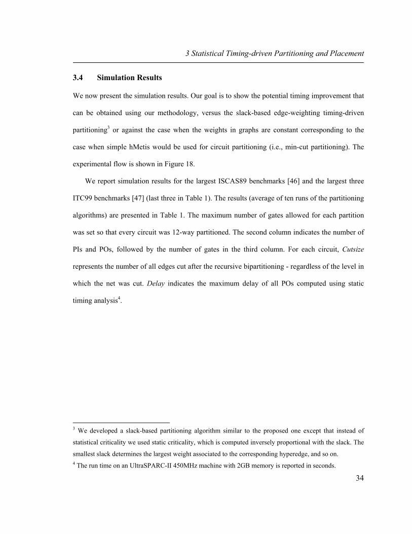
3.4 Simulation Results
We now present the simulation results. Our goal is to show the potential timing improvement that
can be obtained using our methodology, versus the slack-based edge-weighting timing-driven
partitioning3 or against the case when the weights in graphs are constant corresponding to the
case when simple hMetis would be used for circuit partitioning (i.e., min-cut partitioning). The
experimental flow is shown in Figure 18.
We report simulation results for the largest ISCAS89 benchmarks [46] and the largest three
ITC99 benchmarks [47] (last three in Table 1). The results (average of ten runs of the partitioning
algorithms) are presented in Table 1. The maximum number of gates allowed for each partition
was set so that every circuit was 12-way partitioned. The second column indicates the number of
PIs and POs, followed by the number of gates in the third column. For each circuit, Cutsize
represents the number of all edges cut after the recursive bipartitioning - regardless of the level in
which the net was cut. Delay indicates the maximum delay of all POs computed using static
timing analysis4.
3 We developed a slack-based partitioning algorithm similar to the proposed one except that instead of
statistical criticality we used static criticality, which is computed inversely proportional with the slack. The
smallest slack determines the largest weight associated to the corresponding hyperedge, and so on. 4 The run time on an UltraSPARC-II 450MHz machine with 2GB memory is reported in seconds.
3 Statistical Timing-driven Partitioning and Placement
35
Cutsize and delay comparison
Slack based or constant edge weighting
Circuit netlist
Criticality computation
Statistical criticality based edge weighting
partitioning
Criticality update
Figure 18 Simulation setup.
It can be observed that, the proposed partitioning methodology offers on average 11%
improvement in delay. However, this is at the expense of an increase of 21% in the cutsize. The
cutsize increased because the search space of the hMetis partitioner is reduced when criticality is
used as hyperedge weight. The partitioner does not have the same freedom in exploring the search
space as when all hyperedges have the same weight. The run time for our methodology is longer
due to the criticality update operation.
3.5 Partitioning-based Placement
In order to further validate our timing driven partitioning algorithm we integrated it with Capo
[24]. Capo is a leading fixed-die partitioning based placement tool, whose implementation can be
downloaded at [49]. Capo places a circuit by recursively bipartitioning it in a way similar to the
one described by Figure 16.b. However, the actual implementation of Capo is rather complex. It
has incorporated many heuristics for recursive bisection, hierarchical tolerance computation,
block splitting, and terminal propagation. The main objective of the Capo placement algorithm is
to minimize the average half-perimeter wire length (HPWL). A timing-driven version of Capo

3 Statistical Timing-driven Partitioning and Placement
36
appeared in [54], but it is not available in the latest version of Capo whereas the circuits used for
simulation results in [54] are not public. Congestion is indirectly minimized by the min-cut
partitioning algorithms, which are implemented inside Capo. Partitioning of graphs with more
than 200 nodes is done with a multi-level partitioning algorithm. Graphs with 35-200 nodes are
partitioned using a flat FM partitioning algorithm and graphs with less than 35 nodes are
partitioned optimally with a branch-and-bound partitioning algorithm. We developed our
customized Capo placement algorithm by replacing the multi-level and flat partitioning
algorithms with our proposed timing driven partitioning algorithm. Our modified version of Capo
can be run using either our statistical edge-weighting timing driven partitioning algorithm
(presented in Section 3.3), the slack-based edge-weighting timing driven hMetis algorithm or the
traditional min-cut hMetis partitioning algorithm. This provides us with a platform to verify the
effectiveness of the statistical timing-driven partitioning for delay minimization. The fact that we
use hMetis as the partitioning engine in all experiments, makes a level playing-field for the
methods being compared: we are not comparing hMetis to Capo’s internal partitioning algorithm
and the results better show the effect of our timing and criticality modeling. The simulation
results are shown in Table 2.
The final coordinates of the terminals of a net become available with better accuracy as the
partitioning-based placement proceeds. During placement we assign lumped RC Elmore delays to
all cut nets computed using the half-perimeter of the bounding-box. This is different from the
delay computation at partitioning level, described in Section 3.3, which used an estimation
method for the average wire length of every cut net. The delays reported in Table 2 are computed

3 Statistical Timing-driven Partitioning and Placement
37
using the final placement coordinates. Hence, these delays are closer to the real circuit delays
then those reported in Table 15.
It can be seen that the average delay when circuits are placed with the statistical timing-
driven partitioning based placement algorithm is 5% smaller than the delay when circuits are
placed with the traditional min-cut partitioning-based placement algorithm. The HPWL increased
on average about 12% and run-time increased on average about 12%.
The delay decrease is smaller compared to the delay decrease at the partitioning phase,
reported in Section 3.4. The difference can be explained by the fact that, the placement algorithm
has integrated terminal propagation, which is not present during partitioning described in Section
3.4. This results in placing nets with many terminals in smaller bounding-boxes. Therefore, these
nets will have smaller delay irrespective of the partitioning level at which they may be cut.
During timing-driven partitioning, delay decrease tends to be a result of not cutting these nets
especially at early partitioning levels (which however may be cut by the traditional min-cut
partitioning algorithm), which turns into larger delays assigned to them by the estimation
procedure. In this way the delay difference obtained in Section 3.4 may be bigger compared to the
delay computation inside the placement algorithm. The HPWL increase is in agreement with the
cutsize increase obtained in Section 3.4. That is because the increase in cutsize, obtained during
partitioning, translates into bigger bounding-boxes at the placement level.
The longer run-times for the timing driven placement is also in agreement with the longer
run-times obtained in Section 3.4 for partitioning. The run-time overhead is due to both the
5 It is observed that the statistical wirelength estimation used at the partitioning level only in Section 3.4
leads to an overestimation of circuit delays.

3 Statistical Timing-driven Partitioning and Placement
38
criticality update process and the statistical and static timing analyses integrated into the
placement algorithm.
3.6 Summary
We proposed a new edge-weighting based timing-driven partitioning algorithm. Because we
changed the partitioning process itself and we used the hMetis partitioning algorithm our
algorithm is fast, and thus applicable to large-sized circuits. The new delay model better reflects
the timing criticality inside circuits and leads to better circuit performance than the circuits
partitioned using pure hMetis or the slack-based partitioning algorithms. We further validated our
timing-driven partitioning algorithm by integrating it into a placement algorithm.

Tabl
e 1
Part
ition
ing
sim
ulat
ion
resu
lts. D
elay
is c
ompu
ted
usin
g st
atic
tim
ing
anal
ysis
.
C
onst
edg
e-w
eigh
t hM
etis
Sl
ack-
base
d ed
ge-w
eigh
t hM
etis
St
atis
tical
edg
e-w
eigh
t hM
etis
Circ
uit
PI /
PO
No.
Gat
es
Del
ay [n
s]C
utsi
ze
CPU
(s)
Del
ay [n
s] C
utsi
ze
CPU
(s)
Del
ay [n
s]
Cut
size
C
PU(s
) C
ordi
c 23
/2
881
9.73
25
9.20
1.
00
10.2
8 33
3.00
1.
00
8.91
26
3.60
1.
00
Dal
u 75
/16
883
9.03
27
5.00
1.
00
9.04
30
1.00
1.
00
8.19
34
0.80
1.
00
S923
4 39
/16
1257
13
.98
170.
20
1.00
11
.53
182.
20
1.00
11
.47
240.
80
1.00
M
isex
3 14
/14
1349
30
.03
543.
00
1.00
29
.19
545.
80
1.00
24
.86
701.
80
1.00
S1
3207
90
/56
1570
17
.71
160.
40
1.00
15
.32
254.
20
1.00
16
.51
230.
40
1.00
C
5315
17
8/10
6 20
62
12.5
2 34
1.60
2.
00
11.8
8 35
0.00
2.
00
12.3
4 42
0.20
2.
00
C75
52
206/
35
2387
17
.58
310.
40
2.00
16
.94
336.
20
2.00
16
.28
394.
80
2.00
D
es
256/
245
3451
21
.84
443.
40
2.20
20
.81
486.
60
3.00
19
.29
454.
40
3.00
Fr
isc
19/1
6 34
79
85.7
2 67
2.80
3.
00
79.5
8 96
1.40
3.
40
58.5
5 76
6.60
3.
60
C62
88
32/3
2 35
98
45.2
1 27
3.40
2.
00
43.0
3 26
8.00
3.
00
39.6
8 33
2.20
3.
00
Ellip
tic
130/
112
4711
12
6.82
38
7.60
3.
00
126.
82
577.
60
3.00
12
6.82
58
5.40
3.
20
Pdc
16/4
0 48
21
148.
20
1267
.80
4.00
14
8.20
13
32.2
0 5.
00
143.
69
1430
.80
5.00
Ex
1010
10
/10
4898
12
2.53
13
26.8
0 5.
00
121.
08
1454
.40
6.00
11
9.69
15
37.8
0 6.
00
Too_
larg
e 38
/3
6961
39
.96
2448
.60
7.00
38
.22
2624
.40
9.00
40
.73
2625
.40
9.00
S3
5932
35
/32
1130
4 72
.90
1120
.10
8.00
71
.70
1505
.06
9.00
73
.15
1306
.90
9.83
S3
8584
11
5/74
12
701
119.
57
602.
35
10.5
0 11
9.34
10
57.3
4 12
.33
119.
51
664.
65
11.6
3 B
21s
32/2
2 14
606
314.
94
908.
89
13.5
8 31
0.60
10
33.5
5 15
.38
200.
65
1095
.77
16.1
0 B
22s
32/2
2 22
497
780.
82
1210
.14
23.9
3 72
6.93
13
45.7
5 28
.39
460.
36
1554
.79
30.1
8 B
17s
37/3
0 36
547
918.
80
1968
.69
50.9
8 90
7.32
23
88.1
2 56
.89
854.
39
2369
.79
57.3
0 A
vg.
1 1
0.
97
1.20
0.89
1.
21
Su
m
1
1.
14
1.17

Tabl
e 2
Plac
emen
t sim
ulat
ion
resu
lts. D
elay
is c
ompu
ted
usin
g st
atic
tim
ing
anal
ysis
. Sim
ulat
ions
wer
e pe
rfor
med
on
the
sam
e m
achi
ne a
s tho
se in
Sec
tion
3.4.
C
onst
edg
e-w
eigh
t hM
etis
Sl
ack-
base
d ed
ge-w
eigh
t hM
etis
St
atis
tical
edg
e-w
eigh
t hM
etis
C
ircui
t D
elay
[ns]
W
L C
PU(s
) D
elay
[ns]
W
L C
PU(s
) D
elay
[ns]
W
L C
PU(s
) C
ordi
c 7.
69
364.
80
9.20
7.
54
375.
80
11.8
0 7.
33
404.
00
14.1
0 D
alu
8.27
28
3.20
5.
00
8.29
28
9.40
7.
00
8.08
30
0.80
7.
70
S923
4 10
.17
256.
00
7.60
10
.08
274.
60
10.0
0 10
.17
283.
80
10.8
0 M
isex
3 14
.86
600.
60
12.0
0 14
.84
612.
40
16.2
0 12
.77
798.
60
18.4
0 S1
3207
14
.06
484.
20
15.0
0 13
.92
511.
40
19.0
0 13
.37
508.
00
20.5
0 C
5315
11
.49
819.
00
19.0
0 11
.46
854.
20
24.4
0 11
.30
936.
90
26.0
0 C
7552
13
.33
858.
20
23.8
0 13
.12
880.
60
30.6
0 12
.43
948.
70
32.4
0 D
es
10.8
5 17
19.4
0 39
.20
10.7
1 17
35.4
0 51
.60
10.1
7 17
87.1
0 52
.10
Fris
c 30
.72
1713
.80
85.8
0 29
.91
2088
.60
101.
00
29.6
8 19
34.0
0 10
3.20
C
6288
37
.85
658.
00
50.4
0 37
.65
673.
80
62.0
0 37
.08
782.
50
60.6
0 El
liptic
24
.19
1688
.60
92.0
0 22
.60
1968
.00
109.
00
22.0
9 20
28.6
0 10
9.40
Pd
c 34
.78
2868
.80
108.
80
34.0
0 29
39.6
0 12
7.20
31
.80
3256
.88
134.
77
Ex10
10
28.5
1 27
23.6
0 11
4.60
29
.20
2844
.40
136.
20
26.6
0 32
96.9
0 14
0.10
To
o_la
rge
20.5
0 63
05.2
8 20
1.00
20
.23
6402
.85
240.
00
22.1
0 64
88.7
1 24
0.71
S3
5932
21
.11
3162
.66
483.
66
24.0
5 38
57.6
6 53
6.66
22
.48
3440
.40
537.
60
S385
84
22.4
8 34
42.0
0 59
5.75
23
.78
3655
.16
645.
50
21.6
9 35
89.0
0 65
2.50
B
21s
147.
15
4733
.25
935.
00
146.
46
4892
.50
980.
00
139.
18
5452
.75
991.
25
B22
s 16
4.67
76
98.5
0 20
00.5
0 15
0.89
81
57.2
5 21
23.2
5 13
7.60
90
06.0
0 21
30.2
5 B
17s
191.
93
1643
0.71
10
62.2
8 18
0.52
17
881.
00
1325
.50
172.
48
1929
3.50
12
87.7
5 A
vg.
1 1
0.
99
1.06
0.95
1.
12
Su
m
1
1.
11
1.12
4 Path-based Timing-driven Partitioning and Placement
41
4 Path-based Timing-driven
Partitioning and Placement
In this chapter, we present multi-objective hMetis partitioning for simultaneous cutsize and
circuit delay minimization. We change the partitioning process itself by introducing a new
objective function that incorporates a truly path-based delay component for the most critical
paths. To avoid semi-critical paths from becoming critical, the traditional slack-based delay
component is also included in the cost function. The proposed timing driven partitioning
algorithm is built on top of the hMetis algorithm, which is very efficient. Simulations results
show that 14% average delay improvement can be obtained. The proposed timing-driven
partitioning algorithm is again validated by integration with a placement algorithm.
4.1 Introduction
4.1.1 Motivation
The main advantage of net-based partitioning approaches is their efficiency. As we saw in the
previous chapter, net-based partitioning approaches define some criticality value for each net, as a
measure that indicates the degree of its contribution to the circuit delay. The partitioning process
is discouraged from cutting edges with high criticality values, which is similar to minimizing the

4 Path-based Timing-driven Partitioning and Placement
42
bounding box for each critical net. However, the drawback of the net-based technique is that it
loses the global picture. For example, nets that lie on the same critical path are treated in the same
way as when they are on different critical paths. Figure 19 shows an example of a situation in
which net-based techniques fail to consider the whole path in the partitioning process. Assuming
the three paths have the same delay before partitioning, the partitioning process has to cut as few
nets on each path as possible to avoid a high delay on the path. It is clear that the partitioning in
Figure 19.a will result in a larger circuit delay than the one in Figure 19.b, because all three cut
nets belong to the same critical path, hence increasing its delay threefold compared to the solution
shown in Figure 19.b.
(a) (b)
Figure 19 Example of a situation when net-based partitioning approaches fail to differentiate partitionings
with the same cutsize but different delays.
4.1.2 Research Approach
In this chapter, we try to eliminate the above deficiency by modifying the objective function of
the hMetis partitioning algorithm to minimize the cutsize as well as the circuit delay [1], [2]. We
present multi-objective hMetis [56] partitioning for cutsize and circuit delay minimization. Our
timing-driven optimization approach is different from previous work: we modify the objective
function of the hMetis partitioning algorithm to minimize cutsize as well as circuit delay without
performing any netlist alterations (e.g., buffer insertion and gate duplication), though can be

4 Path-based Timing-driven Partitioning and Placement
43
employed after our method partitions the design. We dynamically focus the timing optimization
engine on the K-most critical paths and use timing criticality to characterize each net that lies on
the critical paths. We use the Elmore delay, along with different wire delays at different levels of
partitioning to achieve a more realistic delay model. Our interconnect delay model incorporates a
statistical net-length estimation.
4.2 Multi-objective hMetis Partitioning: Cutsize and Delay Minimization
In this section we present the multi-objective hMetis partitioning algorithm. While the goal of
classic partitioning algorithms is to minimize cutsize – and hMetis performs this task very
efficiently – the multi-objective graph partitioning problem is much more difficult. One of the
main difficulties in performing multi-objective optimization is that no single optimal solution
exists. Instead, an optimal solution exists for each objective in the solution space. Furthermore, an
optimal solution for one objective may require accepting a poor solution for other objectives. The
result is that the definition of a good solution becomes ambiguous. We will adopt the formulation
of a good solution as it appears in [78]:
• It should allow fine-tuned control of the tradeoffs among the objectives.
• The produced partitionings should be predictable based on user’s input.
• It should be able to handle objectives that correspond to quantities that are both of similar as
well as of different natures (e.g., range, variance, sensitivity to changes in partitioning).
In our case we want a partitioning algorithm that can minimize both the number of wires cut
by the partitioning (hence minimizing congestion at placement) and the number of times most
critical paths are cut (minimizing circuit delay). We call our two objectives cutsize C and circuit
delay D that have to be minimized. However, the two objectives are dissimilar objectives, which

4 Path-based Timing-driven Partitioning and Placement
44
means that optimizing C alone does not necessarily imply that D is also optimized and vice-versa.
That is why we adopt the combination-based formulation for multi-objective optimization that is
proposed in [78]. The idea is to combine both objectives into a single objective. That is, if Co is
the optimal solution with respect to the objective C and Do is the optimal solution with respect to
the objective D, then the combined objective will be a linear combination metric Cc given by the
following equation:
oo
c
DDp
CCpC 21 += (1)
Where (p1, p2) is the preference vector. Minimizing Equation 1 attempts to compute a
partitioning such that it is not far away from any of the optimal with respect to any initial
objective. A preference vector of (1, 3) for example, indicates that we need to move at least three
units closer to the optimal partitioning with respect to the delay objective for each unit that we
move away from the optimal partitioning with respect to the cutsize objective. The preference
vector can be used to traverse the distance between the optimal solution points of each objective.
That results in predictable partitioning based on the preference vector as well as fine-tuned
control of the tradeoff between the two objectives.
The delay objective component is expressed as a combination of three factors that directly
influence the delay of a circuit: the delay of the critical paths, the number of times that each
critical path has been cut, and the edge weight of all edges that lie on the critical and semi-critical
paths.
∑ ∑= =
+=||
1 1
cE
i
K
jjjii kDeD γβωα (2)
Where α and β are weighting parameters; ωi is the weight of edge i (derived from the edge slack);
ei is either 0 or 1 depending on whether edge i is cut or not; |Ec| is the number of edges that form

4 Path-based Timing-driven Partitioning and Placement
45
the K critical paths; Dj is the current delay of the j-th critical path; kj is the number of times that
the j-th critical path has been cut so far; and γ is an exponent used for even finer tuning.
Equation 2 combines the advantages of the path-based method, which captures global delay
information, and the advantage of the edge-based method, that can capture timing criticality of
semi-critical paths without enumerating them. Parameters α and β allow us to put more emphasis
on any of the two net-based and path-based components in Equation 2. The number of critical
paths that are enumerated during the recursive partitioning is established based on the circuit
structure, size and, number of pins. A discussion of how to choose K is presented in the next
section.
4.3 Path-based Timing-driven Partitioning
4.3.1 Choosing K-most Critical Paths
Since the number of paths in a circuit is exponential, a path-based timing-driven method has to
focus only on a limited number of K-most critical paths. The problem is, the set of K-most critical
paths is a moving target. After one step of partitioning, some of the paths previously among the
K-most critical become critical, and hence replace some of the paths in the original K-most
critical paths. We considered two strategies: (1) partitioning without updating of the K-most
critical paths during recursive bipartitioning, or (2) updating the list of the K-most critical paths
during recursion. In the first case we initially find the K-most critical paths and then perform all
subsequent recursive bipartioning stages trying to avoid these critical paths from being cut. The
second case is motivated by the fact that the initial K-most critical paths may not remain critical
after the partitioning (or placement and routing) is done [94]. In this case, we identify the current
K-most critical paths at each partitioning level and update the edge weights as well as the path
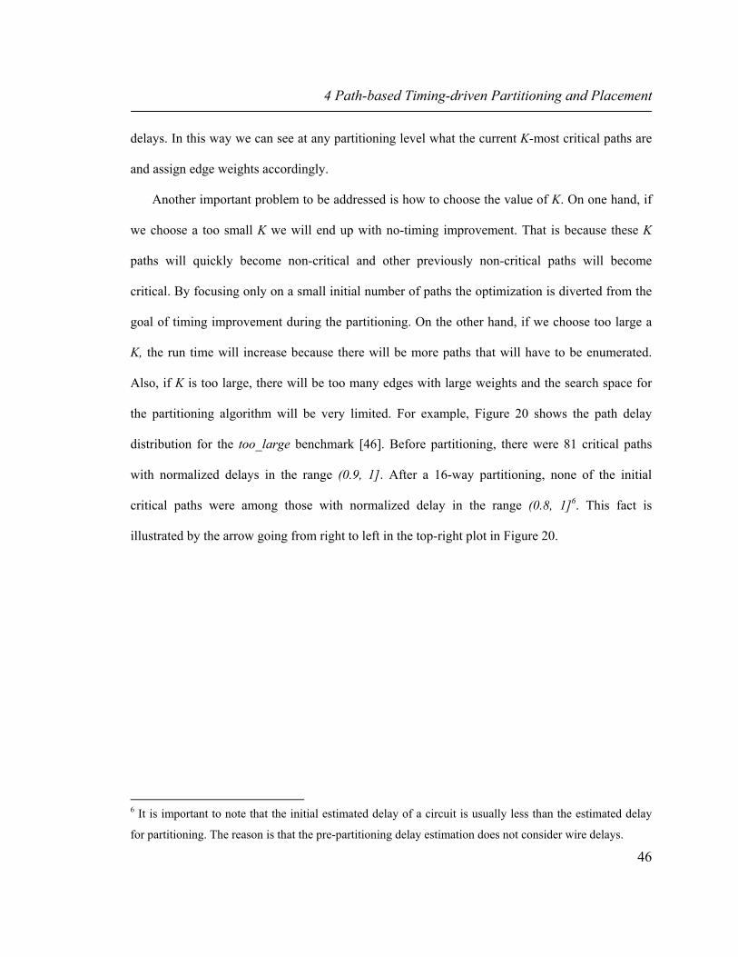
4 Path-based Timing-driven Partitioning and Placement
46
delays. In this way we can see at any partitioning level what the current K-most critical paths are
and assign edge weights accordingly.
Another important problem to be addressed is how to choose the value of K. On one hand, if
we choose a too small K we will end up with no-timing improvement. That is because these K
paths will quickly become non-critical and other previously non-critical paths will become
critical. By focusing only on a small initial number of paths the optimization is diverted from the
goal of timing improvement during the partitioning. On the other hand, if we choose too large a
K, the run time will increase because there will be more paths that will have to be enumerated.
Also, if K is too large, there will be too many edges with large weights and the search space for
the partitioning algorithm will be very limited. For example, Figure 20 shows the path delay
distribution for the too_large benchmark [46]. Before partitioning, there were 81 critical paths
with normalized delays in the range (0.9, 1]. After a 16-way partitioning, none of the initial
critical paths were among those with normalized delay in the range (0.8, 1]6. This fact is
illustrated by the arrow going from right to left in the top-right plot in Figure 20.
6 It is important to note that the initial estimated delay of a circuit is usually less than the estimated delay
for partitioning. The reason is that the pre-partitioning delay estimation does not consider wire delays.

050
010
0015
0020
0025
0030
0035
0040
0045
00
No. of Paths
Norm
aliz
ed D
elay
too_
larg
e (1
4781
)
Initi
alK
Path
s Fi
xed
K Pa
ths
Upda
ted
4 3
2 1
4 3
2 1
...0.
7
0.7
...0.
8
0.8
...0.
9
0.9.
..1
...0.
7
0.7
...0.
8
0.8
...0.
9
0.9.
..1
24
81/8
1
21
79/8
1
17
20
16
2/81
K Pa
ths
Fixe
d
K Pa
ths
Upd
ated
Fi
gure
20
The
path
del
ay d
istri
butio
n fo
r too
_lar
ge (t
otal
num
ber o
f pat
hs is
147
81) b
efor
e an
d af
ter p
artit
ioni
ng, w
hich
is d
one
with
and
with
out u
pdat
ing
the
mos
t crit
ical
pat
hs in
regi
on 1
(0.9
, 1].

4 Path-based Timing-driven Partitioning and Placement
48
The arrows oriented from left to right in the same plot indicate initial non-critical paths that
became critical after partitioning was completed. This is similar to results obtained previously
when this situation was observed after placement and routing were done [94]. However, if we re-
calculate all K-most critical paths at each partitioning level, the above case will happen less
frequently. That is shown in the bottom-right plot in Figure 20, which shows the dynamics of the
most critical paths among paths mainly with large delays (regions 1, 2, 3 in the right side of
Figure 20). Updating the K-most critical paths enables us to concentrate the optimization process
on the “real” K most critical paths at any time at all levels because they are re-enumerated taking
into account all the wire delays that were assigned (the process of assigning wire delays to all cut
nets is described in Section 3.3) to all cut nets during previous partitioning levels.
To further illustrate the effect of updating the K-most critical paths during partitioning, Figure
21 shows the path distribution with respect to circuit delay in both cases (updating vs. not
updating). As we can see the delay obtained after partitioning performed with dynamic updating
the list of the K-most critical paths is smaller than the one obtained without updating the list. The
situation described in the example above is true for all the circuits that we tested. That is why we
decide to perform recursive partitioning while dynamically updating the K-most critical paths at
any partitioning level. In this way we determine a minimal number of critical paths at a certain
partitioning level to become non-critical later on. In our simulations we noticed that we obtain
satisfactory results if we consider as critical only the paths with normalized delays in the (0.95, 1]
range. In cases where the number of paths in this region exceeded 500 we retained only the first
500 paths. The enumeration path algorithm that was implemented is similar to that described in
[51].
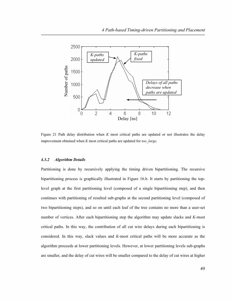
4 Path-based Timing-driven Partitioning and Placement
49
Delays of all paths decrease when paths are updated
K-paths updated
Delay [ns]
Num
ber o
f pat
hs
K-paths fixed
Figure 21 Path delay distribution when K most critical paths are updated or not illustrates the delay
improvement obtained when K most critical paths are updated for too_large.
4.3.2 Algorithm Details
Partitioning is done by recursively applying the timing driven bipartitioning. The recursive
bipartitioning process is graphically illustrated in Figure 16.b. It starts by partitioning the top-
level graph at the first partitioning level (composed of a single bipartitioning step), and then
continues with partitioning of resulted sub-graphs at the second partitioning level (composed of
two bipartitioning steps), and so on until each leaf of the tree contains no more than a user-set
number of vertices. After each bipartitioning step the algorithm may update slacks and K-most
critical paths. In this way, the contribution of all cut wire delays during each bipartitioning is
considered. In this way, slack values and K-most critical paths will be more accurate as the
algorithm proceeds at lower partitioning levels. However, at lower partitioning levels sub-graphs
are smaller, and the delay of cut wires will be smaller compared to the delay of cut wires at higher

4 Path-based Timing-driven Partitioning and Placement
50
partitioning levels. Therefore, the major contribution to circuit delay is due to wires cut at high
levels of partitioning, which in the final circuit layout represent global wires. Thus, it is especially
important to update slacks and re-enumerate K-most critical paths at higher levels of partitioning.
In our simulations, slacks and K-most critical paths are updated at each bipartitioning step at the
first four partitioning levels and then once for each partitioning level in order to maintain the run-
time reasonable while achieving satisfactory accuracy.
Because the result of the first partitioning step has a great impact on the final delay (as it
represents the starting solution for all subsequent partitioning levels), it is especially important at
this level not to cut nets that will have assigned large delays. On the other hand, nets that do not
lie on the K-most critical paths can introduce large delays in case that they are cut. This may limit
the potential delay decrease that can be obtained. We have integrated a look-ahead like technique,
which we use at the first partitioning level only to keep the run time low, and which performs the
first bipartitioning more times as follows. First we start with slacks computed considering zero
wire delays and K-most critical paths. After bipartitioning is done, the K-most critical paths are
updated and their kj’s (see equation 2) are computed. Vertices on previous K-most critical paths
are fixed in their partitions and the rest of vertices are set free. If there are vertices on the new K-
most critical paths that were on the previous K-most critical paths they are set free. All wire
delays are reset to zero but the values of kj’s are kept. Then, bipartitioning is performed again.
This process continues until a certain number of vertices become fixed or a certain number of
iterations are performed. For each such top-level bipartitioning, we record the delay. When the
top-level bipartitioning iteration stops, we continue at the second partitioning level with the
partitioning that offered the best delay at first partitioning level. The delay model is the same as
presented in Chapter 3, and its detailed description is found in Appendix B.

4 Path-based Timing-driven Partitioning and Placement
51
4.4 Simulation Setup and Results
In this section we describe the timing driven partitioning simulation setup and present simulation
results.
4.4.1 Simulation Setup
The simulation setup is shown in Figure 22. We start with a netlist of a circuit that was first
optimized using script.rugged in SIS [80]. Then, we perform recursive bipartitioning using either
the pure hMetis algorithm or the multi-objective hMetis. Finally we compare the partitioning
obtained in both cases in terms of cutsize and circuit delay.
Cutsize and delay comparison
Pure hMetis bipartitioning (constant edge weights)
Circuit netlist
K-most critical paths enumeration & slack based
weight computation
Multi objective hMetis
partitioning
K-most critical paths re-enumeration and
slack update
Figure 22 Simulation setup for comparison of our proposed multi-objective hMetis partitioning algorithm
to pure hMetis algorithm.
4.4.2 Simulation Results
We report simulation results for the circuits shown in Table 3. Simulations results are reported for
three different cases.
• Net-based: The first case represents a pure net-based partitioning approach. In this case, we
assign weights to all hyperedges inversely proportional to their slack values (i.e., The

4 Path-based Timing-driven Partitioning and Placement
52
smallest net slack in the circuit determines the largest hyperedge weight and the largest slack
net is assigned the smallest weight. By assigning hyperedge weights in this way, this case
falls into the category of net weighting, whose purpose is to determine hMetis algorithm to
cluster the most critical hyperedges early, which means that they would not be cut by the
partitioning process. This is different from net budgeting technique, which translates path
constraints into either length or timing upper bounds for each net using a delay budgeting step
[77]). There is no path information transmitted to hMetis in this case.
• Net-based via path-counting case implements a recently proposed novel net weighting
technique [59].
• Path-based: The third case represents a pure path-based partitioning approach. In this case K-
most critical paths are updated dynamically, and transmitted to hMetis as dictated by
Equation 2. Hyperedges that lie on any of the K-most critical paths have weights assigned as
in the first case while the rest of edges have constant weights.
• Net+Path-based: The last case represents a net-path-based partitioning approach. This case
practically combines the first and third cases: K-most critical paths are transmitted to hMetis
while all hyperedges have weights assigned as in the first case. We expect to obtain large
delay decrease, especially with the third approach because it implements the multi-objective
partitioning algorithm, described in Section 4.3, and uses additional timing information for
hyperedges that do not lie on the K-most critical paths. These three cases are compared to the
standard pure hMetis algorithm.
Simulations results for delay, cutsize and run-time are shown in Table 3 for 16-way
partitioning. For each circuit, Delay indicates the maximum delay of all PO’s. The Cutsize
represents the number of all hyperedges cut after the recursive bipartitioning. All results in the

4 Path-based Timing-driven Partitioning and Placement
53
table are the average of ten different runs on a Pentium dual-CPU, 1.5 GHz with 2GB of memory.
We observe the trade-off between delay, on one hand, and cutsize and run-time on the other hand.
It can be seen (see also Figure 23 and Figure 24) that the proposed partitioning methodology
improves delay by 14% on average. However, this is at the expense of an increase in cutsize and
run-time degradation, but the runtime is still very reasonable.

Tabl
e 3
Com
pari
son
betw
een
our m
etho
ds a
nd p
ure
hMet
is.
D
elay
[ns]
C
utsi
ze
CPU
(s)
Circ
uit
PI /
PO
No.
of
gate
s Pu
re
hMet
is
Net
- ba
sed
Net
-ba
sed
via
path
-co
unt
Path
- ba
sed
Net
and
Pa
th
Bas
ed
Pure
hM
etis
N
et-
base
d
Net
-ba
sed
via
path
-co
unt
Path
- ba
sed
Net
an
d Pa
th
Bas
ed
Pure
hM
etis
N
et-
base
d
Net
-ba
sed
via
path
-co
unt
Path
- ba
sed
Net
an
d Pa
th
Bas
ed
mis
ex3
14/1
4 13
49
67.6
0 63
.66
61.5
0 59
.91
61.1
6 54
3 53
0 66
4 66
9 61
4 5
8 9
13
13
x3
135/
99
1369
18
.78
16.6
5 16
.88
16.9
0 16
.65
211
270
248
245
261
4 5
5 6
6 s1
3207
90
/56
1570
20
.20
16.8
3 20
.10
20.3
2 18
.72
234
259
218
243
303
12
17
16
58
63
c628
8 32
/32
2435
59
.21
55.1
3 54
.04
55.2
0 56
.26
182
182
205
215
216
31
50
37
76
80
s158
50
39/7
5 43
21
81.1
4 78
.85
78.8
8 73
.61
78.9
3 61
7 69
9 62
1 62
2 67
1 28
36
31
35
37
fr
isc
19/1
6 44
00
169.
33
150.
95
188.
24
168.
30
150.
20
838
923
888
910
869
34
65
38
68
61
ellip
tic
130/
112
4711
27
1.02
27
1.02
27
1.00
26
0.25
20
5.25
50
8 54
7 55
1 54
2 61
9 16
20
17
20
22
ex
1010
10
/10
4898
35
4.22
33
8.25
33
4.06
30
4.50
33
1.75
13
07
1260
14
33
1734
15
14
21
30
30
45
49
pdc
16/4
0 48
21
409.
29
416.
99
416.
75
379.
24
384.
50
1750
16
22
1704
20
42
1847
31
36
40
49
52
to
o_la
rge
38/3
69
61
112.
91
103.
52
92.6
2 11
1.50
97
.62
2566
24
59
2472
28
19
2470
20
33
35
43
45
s3
5932
19
2/11
0 73
33
315.
61
315.
61
203.
22
130.
61
135.
83
491
646
954
1171
10
43
24
40
41
112
121
s385
84
35/3
2 11
304
257.
27
265.
31
255.
05
190.
04
197.
86
671
1115
57
7 19
18
1999
33
48
44
16
1 18
9 s3
8417
11
5/74
12
701
567.
12
537.
75
566.
98
529.
00
527.
25
198
274
198
232
298
18
40
32
34
38
b21s
32
/22
1560
4 11
09.6
2 11
91.0
0 11
89.0
0 49
4.00
51
2.25
84
5 85
7 83
9 87
2 91
5 45
7 79
6 69
8 70
5 84
8 b2
2s
32/2
2 23
892
2275
.50
2220
.75
2210
.25
1667
.00
2005
.75
1108
12
47
1136
11
54
1136
53
4 92
6 88
8 12
50
1400
b1
7s
37/3
0 39
390
2606
.84
2573
.75
2524
.00
2412
.25
2406
.34
1780
24
46
1732
18
41
1882
51
8 24
82
2010
29
87
2991
b1
8s
36/2
2 10
7979
15
51.6
0 19
09.5
0 16
70.0
0 16
09.5
0 13
33.5
0 17
17
1730
17
38
1712
17
17
860
2025
19
87
2365
30
76
Avg
.
1
0.98
0.
95
0.86
0.
84
1 1.
14
1.08
1.
28
1.3
Su
m
1 2.
5 2.
25
3 3.
4

4 Path-based Timing-driven Partitioning and Placement
55
0
500
1000
1500
2000
2500
3000
mis
ex3 x3
s132
07
c628
8
s158
50
fris
c
ellip
tic
ex10
10 pdc
too_
larg
e
s359
32
s385
84
s384
17
b21s
b22s
b17s
b18s
Del
ay
Pure hMetis Net-based Path-based Net+Path-based
Figure 23 Delay results comparison.
0
500
1000
1500
2000
2500
3000
mis
ex3 x3
s132
07
c628
8
s158
50
fris
c
ellip
tic
ex10
10 pdc
too_
larg
e
s359
32
s385
84
s384
17
b21s
b22s
b17s
b18s
Cut
set
Pure hMetis Net-based Path-based Net+Path-based
Figure 24 Cutsize results comparison.

4 Path-based Timing-driven Partitioning and Placement
56
4.5 Partitioning-based Placement
In order to further validate our timing driven partitioning algorithm we integrated it with Capo,
similarly to the approach in Section 3.5 of Chapter 3. We developed our customized Capo
placement algorithm by replacing the multi-level and flat partitioning algorithms with our
proposed multi-objective partitioning algorithm. Our modified version of Capo can be run using
either our timing driven partitioning algorithm or the traditional min-cut hMetis partitioning
algorithm. Since our timing driven partitioning algorithm is built on hMetis, we want to compare
placements of the same circuits obtained when Capo uses either the proposed multi-objective
partitioning hMetis or the traditional min-cut hMetis partitioning algorithm (Our pure min-cut
hMetis placement results are worse than Capo. The reason is that the partitioning algorithm in
Capo is well tuned for placement ). The simulation results are shown in Table 4.
Table 4 Timing driven partitioning placement vs. min-cut driven partitioning placement.
Ratio between our and min-cut partitioning-based placement algorithms Circuit Delay (best out of 6 runs) Delay (avg. of 6 runs) HPWL CPU(s) misex3 0.82 0.83 1.46 1.25 x3 1.02 1.01 1 1.5 s13207 0.96 0.95 1.1 1.52 c6288 0.99 1.01 1.23 1.44 s15850 0.94 0.92 1.3 1.28 frisc 0.87 0.85 1.65 1.51 elliptic 0.93 0.93 1.44 1.59 ex1010 1.03 1.01 1.76 1.39 pdc 0.91 0.98 1.68 1.63 too_large 1.08 1.03 1.29 1.54 s38417 0.97 0.97 1.1 1.36 s38584 0.92 0.91 1.1 1.64 s38417 0.94 0.98 1.39 1.8 b21s 0.88 0.88 1.29 1.69 b22s 0.83 0.83 1.33 1.57 b17s 0.81 0.88 1.09 2.02 b18s 0.85 0.82 1.15 4.71 Avg. 0.93 0.93 1.32 x1.73

4 Path-based Timing-driven Partitioning and Placement
57
Because the coordinates of all terminals of every net are available during placement, we can
compute the Elmore delay for each net using the half-perimeter of its bounding-box. Note that
this is different from the delay computation at the partitioning level described in Section 4.3.2,
which used an estimation method for the average wire-length of every cut net. It can be seen that
the average delay when circuits are placed with the timing-driven partitioning based placement
algorithm is 7% smaller than the delay when circuits are placed with the traditional min-cut
partitioning-based placement algorithm. The half-perimeter wire-length (HPWL) increased on
average by 32% and the run-time increased on average by less than two times. The difference
between the delay decrease obtained at the placement level and the delay decrease obtained at the
partitioning level, in Section 4.3.2, may be explained as follows. The placement algorithm has
integrated terminal propagation, which is not present during partitioning described in Section
4.3.2. This makes nets with many terminals to be placed within smaller bounding-boxes.
Therefore, these nets will have smaller delays irrespective of the partitioning level at which they
may be cut. During timing-driven partitioning, delay decrease tends to be a result of not cutting
these nets especially at early partitioning levels (which however may be cut by the traditional
min-cut partitioning algorithm), which turns into larger delays assigned to them by the estimation
procedure. In this way the delay difference obtained in Section 4.3.2 may be larger compared to
the delay computation inside the placement algorithm. The HPWL increase is in agreement with
the cutsize increase obtained in Section 4.3.2. That is because the increase in cutsize, obtained
during partitioning, translates into bigger bounding-boxes at the placement level. The longer run-
times for the timing driven placement is also in agreement with the longer run-times obtained in
Section 4.3.2 for partitioning. The run-time overhead is due to both the path enumeration process
and the static timing analysis integrated into the placement algorithm.

4 Path-based Timing-driven Partitioning and Placement
58
4.6 Summary
We proposed multi-objective hMetis partitioning algorithm for cutsize and circuit delay
optimization. The proposed algorithm is efficient and applicable to large-sized circuits. It
performs better timing-driven partitioning because it considers path delays as opposed to slack-
based approaches. It does not determine area increase because it does not use netlist alteration as
previous approaches but only due to an increase of the average wirelength. The proposed timing-
driven partitioning algorithm was integrated with a partitioning-based placement algorithm.

5 Placement for Robustness Predictability and Performance
59
5 Placement for Robustness
Predictability and Performance
In this chapter, we study the relationship between robustness, predictability and performance of
VLSI circuits. It is shown that predictability and performance are conflicting objectives.
Performance and robustness are statically conflicting objectives but they are statistically non-
conflicting. We propose and develop means for changing a standard timing-driven partitioning-
based placement algorithm in order to design more predictable and robust circuits without
sacrificing much of performance.
5.1 Introduction
5.1.1 Motivation
Ideally, we would like a design methodology to offer predictable and robust designs at the best
performance. High robustness means that performance of the design is less influenced by noise
factors and remains within acceptable limits, i.e., the design is more tolerant to perturbations -
such as process variations, temperature and supply voltage changes - and therefore more reliable.
We would also like our design methodology to be predictable. Accurate estimation
techniques would allow correct decisions early in the design process, which would result in fast

5 Placement for Robustness Predictability and Performance
60
design convergence. Predictability is to be achieved in the face of design uncertainties, which are
caused by either incomplete system specification or inherent difficulty of estimating performance
metrics during the optimization process.
5.1.2 Previous Work
Several ways of defining predictability or uncertainty have been proposed. Uncertainty was
considered as the unpredictable process variations, which can cause delays to change from their
nominal values [14]. Srivastava and Sarrafzadeh define predictability as the quantified form of
the accuracy of the cost function estimation [84]. In the context of floorplanning, Bazargan et al.
describe uncertainty as multiple values for heights and widths of the same module, and the goal is
to minimize a linear combination of the expected value and the standard deviation of the area of
the floorplan [16]. Wang et al. consider uncertainty at the placement level as the incomplete
information about modules in the netlist [91]. To make routing more predictable at the placement
level, one can use techniques for increasing the flexibility of rectilinear Steiner trees [21]. Kahng
et al. describe signals as having no uncertainty when they all arrive simultaneously, which means
the output of the cell has little or no uncertainty [53]. However, when the uncertainty of the
signals varies simultaneous arrival of all signals will actually cause greater average and standard
deviation of the output cell distribution [45]. A design process is considered predictable in [82]
when the analytical or statistical predictive tools are accurate and allow providing constraints for
the following design steps.

5 Placement for Robustness Predictability and Performance
61
5.1.3 Research Approach
In this chapter we analyze the relationship between robustness, predictability and performance
(optimality) and seek means for their control [4]. We apply our methodology to timing-driven
partitioning-based placement in order to design predictable and robust circuits. We regard the
optimization process under uncertainty as the iterative computation of a number of objective
functions, which depend on variables whose values are known within a range of values (i.e., as
probability distributions or as intervals within which these variables lie). Predictable design
means the ability to accurately compute the objective function (within the chosen modeling
framework), and to find means of making current estimations closer to the real final values. We
use the standard deviation (standard deviation - fraction of the mean delay value) as the measure
of predictability of the overall circuit delay distribution at the primary outputs, as well as at the
output of each cell inside the circuit. This means that the smaller the standard deviation, the more
predictable is the delay. The slope of the variation of the standard deviation of the overall circuit
delay, when gate and wire delays change, characterizes the robustness of the circuit.
We use statistical timing analysis (see Appendix A for a detailed description) as a modeling
framework for the purpose of characterizing circuits from the predictability and robustness
perspectives.
5.2 Predictability Analysis
To understand the mechanisms behind the interaction between the statistical addition and
maximum operations and the predictability of a circuit we performed some studies. Initially, our
focus is on two very simple toy-cases: (1) a chain (e.g., path) of delay elements and (2) a generic
gate with a given number of input pins with statistical arrival times. The output of the first case is

5 Placement for Robustness Predictability and Performance
62
calculated by successive statistical add operations, while the output of the second case is
computed using the statistical max of the inputs, followed by the statistical addition of the gate
delay. In each case, we want to find the variation of the standard deviation at the output σout when
the standard deviation of the delay elements vary, for different values of the number of delay
elements (or inputs) m. When the standard deviation of the delay elements vary within [5%, 50%]
of their means, the output standard deviation σout varies as shown in Figure 25.
Observation 1: We note that for large standard deviation of gate and wire delays (larger than
about 9%), circuits that consist of gates with larger number of inputs show more robustness and
better predictability (Figure 25.b). On the contrary, when gate standard deviation is small, fewer
inputs translates into better robustness.
This observation has an implication for CAD developers: it can be used in a physical
synthesis process to minimize circuit delay variations. Gates that are placed in regions with high
temperature variations (e.g., close to a floating-point unit that is active only part of the time), and
hence larger delay variations, can be mapped to large fanin gates in the library. Note that mapping
gates to larger fanin gates could have a negative impact on the area or even delay of the circuit.
Hence, the technology mapping process has to be done judiciously.

5 Placement for Robustness Predictability and Performance
63
(µ1,σ1) (µ2,σ2) (µm-1,σm-1) (µm,σm)
(µout,σout) (µ1,σ1) (µ2,σ2) (µm,σm)
(µout,σout)
Input Standard Deviation [%]
Stan
dard
Dev
iatio
n of
“ad
d” [%
]
(a) (b)
Stan
dard
Dev
iatio
n of
“m
ax”
[%]
Input Standard Deviation [%]
Figure 25 (a) Standard deviation at the output σout of a series of m delay elements (b) Standard deviation at
the output of a gate with m inputs
Observation 2: Better predictability and robustness is obtained for interconnects with more
buffers (Figure 25.a). Furthermore, smaller wire and inverter delay variations results in smaller
output variation.
The observation is good news for interconnect optimization and it says that more buffers not
only helps in reducing the delay; it also helps reduce the variation at the output. Furthermore, this
observation confirms the intuition that the uncertainty adds up: the more uncertainty individual
elements in a path have, the more uncertain the output would be. It is important to note that
observation 2 should not be generalized to any chain of gates with possible converging paths. As

5 Placement for Robustness Predictability and Performance
64
will be shown in Figure 25.a, more elements on the chain does not necessarily result in smaller
deviation at the output.
Next, we analyze the behavior of σout when two elements in the chain vary in opposite
directions. This situation can happen when the length of a net increases while the length of a
different net decreases but the sum of both remains the same (e.g., inverter free to move to left or
right in Figure 26.a). A similar situation can appear among the delay elements at the inputs of a
gate when the decrease in a latest arrival time at one input can be at the expense of the increase of
one at another input (e.g., gate free to move to left or right in Figure 26.b).
(µ1,σ1) (µ2,σ2) (µm-1,σm-1) (µm,σm)
(µout,σout) (µ1,σ1) (µ2,σ2) (µm,σm)
(µout,σout)
(a) (b)
l1 l2 l3
free
σout
l1 l2 l3
fixed free g1
g2
σout
Figure 26 Study cases.
The simulation result of the two cases is shown in Figure 27. Plots in Figure 27.a show that
the standard deviation at the output of a chain is minimum when l2=l3 and that it is better
observable when the standard deviation of the elements in the chain increase (bottom). This is
true as long as the contribution to σout of the two changing delays is significant (i.e., comparable
to the contribution of the rest of delay elements - small values on y axis). When the contribution

5 Placement for Robustness Predictability and Performance
65
to σout of the two changing delays is very small (e.g., wire delay of wires of lengths l2 and l3 are
much smaller than the wire delay of wire l1 and the gate delays), the plots become almost flat (for
large y in Figure 27) because the effect of length change of wires of length l2 and l3 would be
absorbed by the computation of the overall σout. When the delay elements are latest arrival delays
at the inputs of a gate (Figure 27.b), and the contribution to σout of the two changing delays is
significant, the minimum σout is achieved when l2=l3 only for large standard deviation (>9%) of
all delay elements. For small standard deviation of all delay elements, the minimum σout is
achieved at the extremes when l2=0, l3=max length or l2=max length, l3=0.
Observation 3: Plots in Figure 27 suggest the following intuition to be used in a placement
algorithm. To minimize the standard deviation of the gate output delay, the LATs at its inputs
should be equalized (Figure 27.b). Furthermore, the delays of the wires on a critical path should
be equalized so that the output deviation is minimized (Figure 27.a). Observation 3 implies that
the placement method should be aware of statistical slack distributions.
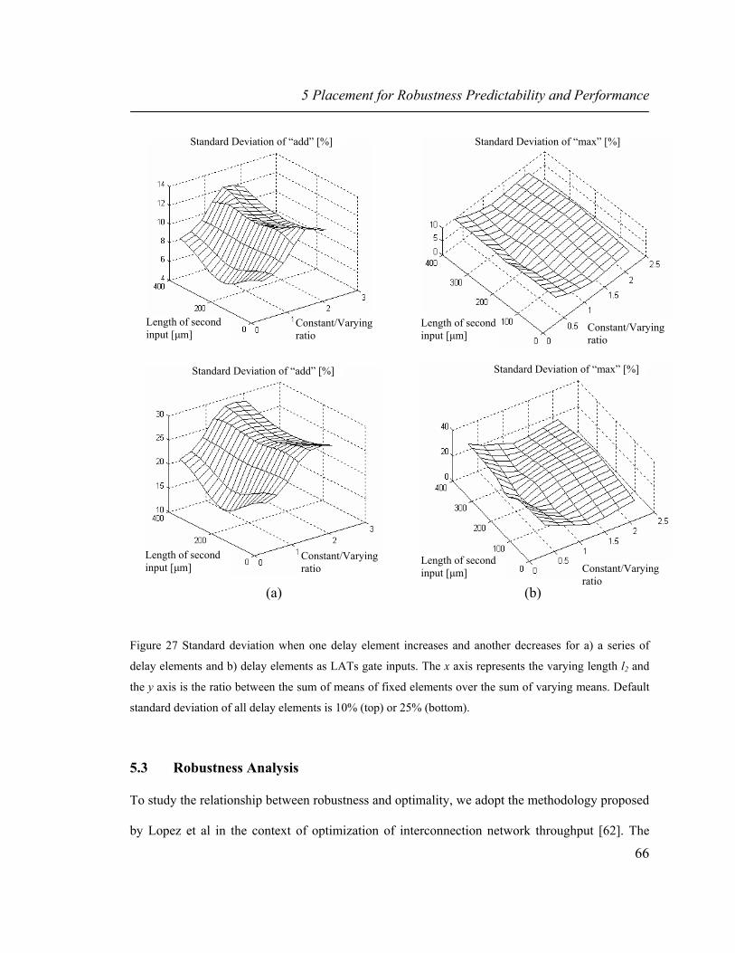
5 Placement for Robustness Predictability and Performance
66
(a) (b)
Standard Deviation of “add” [%]
Length of second input [µm]
Constant/Varying ratio
Standard Deviation of “add” [%]
Length of second input [µm]
Constant/Varying ratio
Standard Deviation of “max” [%]
Length of second input [µm]
Constant/Varying ratio
Standard Deviation of “max” [%]
Length of second input [µm] Constant/Varying
ratio
Figure 27 Standard deviation when one delay element increases and another decreases for a) a series of
delay elements and b) delay elements as LATs gate inputs. The x axis represents the varying length l2 and
the y axis is the ratio between the sum of means of fixed elements over the sum of varying means. Default
standard deviation of all delay elements is 10% (top) or 25% (bottom).
5.3 Robustness Analysis
To study the relationship between robustness and optimality, we adopt the methodology proposed
by Lopez et al in the context of optimization of interconnection network throughput [62]. The

5 Placement for Robustness Predictability and Performance
67
idea of a robust design methodology is to study the effect of factors on the performance and the
interactions between such factors. The key point of such an analysis is to correctly identify and
classify variables that affect the design performance within the modeling framework of the
optimization problem. These variables are classified into two categories: controlled factors and
noise factors. Controlled factors are design parameters that can be controlled directly or
indirectly. Noise factors are random effects that cause performance variation. In the case of the
timing driven placement, the response variable is the overall circuit delay, which should be
minimized.
In what follows, we focus our attention on a generic gate (Figure 26.b - top). For simplicity,
we use the maximum difference between the latest arrival times at the inputs of the gate as a
control factor (i.e., the length of the range [min, max] within which all latest arrival times lie,
called the input range). We choose input range because of three reasons. First, it would allow
pursuing the same objective as in the case of predictability as illustrated in Figure 27.b. Secondly,
this factor can be indirectly controlled during placement. The placement algorithm can control the
lengths of all nets along paths and thus perform a delay budgeting, which affects the latest arrival
times at any point inside the circuit. Finally, the selection of this control factor was suggested by
the results obtained by Hashimoto et al. [45] and Bai et al. [14]. The noise factor is chosen as the
standard deviation of gate and wire delays. Other possible noise factors, not considered in this
experiment include: correlations between lines inside the circuit due to fanout re-convergence,
approximation of the density function of all gate and wire delays with the normal distribution and,
input patterns applied at the primary inputs of the circuit, which may not be known during the
design.

5 Placement for Robustness Predictability and Performance
68
The first part of the experiment consists of selecting three different values for the control
factor, simulating the model of the gate, generating groups of output samples for each of the three
values of the control factor, and analyzing them. We constructed a toy-case using a three-input
gate7 where the control factor (i.e., input-range) can have one of the values 0, 0.5, 1 for a gate
with three inputs determined by the following three sets of LATs: 10,10,10, 9.7,9.7,10.2,
9.5,10,10.58. The value of “0” for the input-range represents the case when the latest arrival
times have equal means, therefore the input-range is zero, and so on. After the gate model is
simulated, groups of 10000 samples of the output delay are generated for each value of the
control factor. These groups are then analyzed using ANalysis Of VAriance9 (ANOVA) method
using Matlab [48]. Figure 28.a shows the significance of the control factor.
The plot in this figure shows that the smallest mean (i.e., 12.73 shown on top of Figure 28.a)
for the gate delay is obtained when the input-range is 0.5. In this case, the set of latest arrival
times 9.7,9.7,10.2 is, from a statistical perspective, better than the set 10,10,10. Note that
static timing analysis would choose 10,10,10 as the best because it has a static delay of 10.
Controlling the input-range as a control factor can be used in a placement algorithm to achieve a
robust design that is less sensitive to delay variations.
The second part of the experiment studies the interaction between the control and the noise
factors. Figure 28.b shows the impact of the noise factor on the mean delay at the output of the
gate for the three different values of the control factor. It can be seen that when the input range is
0.5, the slope of the output delay is smaller than the slope in the case when the input-range is 0. 7 We performed similar analyses for gates with different number of inputs and similar results were
obtained. We restrict our presentation to the three-input case for simplicity. 8 The actual delay value (i.e., 10), is not relevant. Only the range matters. 9 ANOVA is a well-known statistical method for studying the effect of control factors on the average value
of the response variable, which in our case is the mean delay [62], [48].

5 Placement for Robustness Predictability and Performance
69
This means that the delay at the output increases at a higher rate when the LATs at the inputs are
equal. Therefore, the gate is more robust to variations when the input-range is different from zero.
In other words, if our modeling is based on static timing analysis, optimality (best cell delay is
obtained when the input-range is zero) and robustness (cell is more robust for input-range 0.5 -
Figure 28.b) are conflicting objectives. On the other hand, if our modeling is based on statistical
timing analysis, optimality (middle box in Figure 28.a) and robustness (case 0.5 in Figure 28.b)
are non-competing objectives.
(a) (b)
Del
ay [p
s]
Input Standard Deviation [ % ] 0 0.5 1 Input range of LATs
Del
ay [p
s]
Output mean delay [ 12.8408 12.7336 12.9553
Figure 28 (a) Average output delay of a three-input gate with input LAT range of 0, 0.5, and 1 (b) Average
cell delay for the combination of the control factor with the noise factor.
Results in the above analysis are in agreement with those obtained in [45] and exploited for
circuit slack optimization in [14]. These results give us insight into the mechanisms, which
determine a design to be more optimal or more robust and helps in identifying means for

5 Placement for Robustness Predictability and Performance
70
controlling them. It is often more costly to control causes of variations than to make a design
process less sensitive to these variations.
5.4 Case Study: Partitioning-based Placement
We now describe how we can develop means for modifying a standard partitioning-based
placement algorithm in order to achieve more predictable and robust circuits. Based on the
analyses presented in the previous sections, we propose a new net-weight assignment scheme that
we integrated into a timing-driven partitioning-based placement tool. The goal is to change the
behavior of the placement such that the final placement solution is predictable and robust without
sacrificing too much performance. Our placement tool is a modified version of Capo [24]. We
developed our customized Capo placement algorithm by replacing the multi-level and flat
partitioning algorithms of Capo with a timing-driven version of hMetis, a leading partitioning
algorithm [56]. Timing is minimized using timing criticalities (slack-based10) as net-weights
inside the partitioning engine.
Two main observations are the basis for our motivation in the derivation of our new net-
weight assignment scheme. The first observation is that the closer a wire is to the POs, cutting it
is likely to have greater impact on the circuit delay, as it is more likely to lie on many different
critical paths11. Second, standard deviation of the latest arrival times on timing paths decreases
from PIs towards POs for large standard deviation for all wire and gate delays inside the circuit.
However, the decreasing trend is not maintained for small standard deviation That is shown in
10 Timing criticality is computed as inversely proportional to slack. The smallest slack determines the
largest weight associated to the corresponding net, and so on. 11 This observation was directly derived from our placement experiments, and not from the analyses in the
previous sections.

5 Placement for Robustness Predictability and Performance
71
Figure 29.a, which depicts the standard deviation of the latest arrival times at intermediate nodes
on the most critical path for typical standard deviation of 25% and 5% for two different
placements of the circuit too_large. It can be observed that as the statistical timing analysis
advances towards POs with the computation of the latest arrival times, standard deviation tends to
converge to values within a convergence-region. By comparing Figure 29.a to Figure 25.b, we
can see that the behavior of a chain of inverters is quite different from a path with gates of
different sizes and with converging fanins.
It can be seen in Figure 29.a that for small standard deviation of the LATs at the inputs of a
gate, the statistical maximum operation increases with depth. However, for large standard
deviation values, the standard deviation of the intermediate nodes along the path actually
decreases. The difference in behavior of small and large standard deviation values is similar to
what we can observe in Figure 29.b, which is the enlarged bottom-left corner of Figure 25.b. For
small (large) values of standard deviation, gates with smaller (larger) number of inputs can better
tolerate input variations. Gates at small (large) depths of the circuit show a similar statistical
behavior as gates with smaller (larger) fanins.
In order to develop a methodology that minimizes output variations, we have to consider two
factors: (1) how we can affect the deviation (the control factor discussed in Section 5.3), and (2)
how effective our effort would be in minimizing the deviation at the output of a gate (Figure
29.a). We can control the deviation by affecting how close are the latest arrival times at the inputs
of a given gate. Furthermore, the position of the gate on the path (close to PIs or POs) indicates
how much influence we would have on optimizing the deviation. Therefore, for large (small)
standard deviation values, we would like gates close to the PIs (POs) have their latest arrival

5 Placement for Robustness Predictability and Performance
72
times as close as possible in order for the maximum operation to provide the smallest standard
deviation (see Figure 27.b).
(b)
Input Standard Deviation [ % ]
Stan
dard
Dev
iatio
n of
“m
ax”
[%]
(a)
Logic depth
Stan
dard
Dev
iatio
n at
nod
es o
n pa
th [
%]
Figure 29 (a) Standard deviation of LATs at nodes on critical path for too_large for 25% and 5% standard
deviation for wire and gate (b) Enlarged bottom-left corner of Figure 25.b.
The delay of an input can be controlled by changing the bounding box of the net connected to
it (in a partitioning-based placement algorithm, cutting a net at a higher level results in larger
bounding box). Our new net-weight assignment scheme for large standard deviation is described
by the following equation:
)( lati
slackiii wwBw ⋅+⋅⋅= βα (3)
where, Bi is a biasing factor to emphasize weights of nets driven by nodes close to the PIs (nodes
with small logic depths). The classic slack-based net-weight component is slackiw and lat
iw is the
“lat” net-weight component, which is introduced to achieve LATs equalization at the inputs of

5 Placement for Robustness Predictability and Performance
73
gates (nodes) with small logic depths. Parameters α and β are used to put more weight on the
“slack” or the “lat” weight components.
The biasing factor B will have values such that nets at large logic depths are cut more easily
in order to capture the phenomenon of decrease of the standard deviation of the propagated LATs
as described in the beginning of this section. At small logic depths (where the standard deviation
of propagated LATs and the default standard deviation of gate and wire delays are large - Figure
29.a) we put more emphasis on the “lat” net-weight component, which accounts for equalization
of LATs in order to decrease the standard deviation as shown in Figure 27 - bottom and to
achieve robustness as described in Section 5.3).
5.5 Simulation Results
We report simulation results obtained with the placement algorithm described in the previous
section for a set of MCNC91, IWLS93 [46] and ITC99 [47] (last two in Table 5) circuits in two
different scenarios. In the first scenario after the circuit is placed we set all gate and wire delays
as samples of the corresponding distributions. This case mimics the manufacturing process when
gate and wire delays can vary due to process variations [85]. In the second scenario we model
the increase of gate and wire delays due to temperature increase. We consider a pattern where
gate and wire delays increase by 25% (Interconnect Elmore delay increases approximately 5% for
every 10°C increase and current designs can drive the operating temperature to higher than 100°C
[88].) at the center of the chip, by 5% at the boundaries, and y 10% elsewhere. Although the
temperature pattern on a chip can be different and the increase of delay larger [10] [26], we
consider a rather simple pattern for simplicity. The simulation results (average of ten different
runs) are presented in Table 5. After the placement is performed using the classic placement

5 Placement for Robustness Predictability and Performance
74
algorithm and our placement algorithm we compute the circuit delay denoted as Delay (static
delay is computed using the Elmore delay for the lumped RC wire model and the half perimeter
of the bounding box for the wire-length of a net) using the static timing analysis. Then, we model
gate and wire delays as random variables and perform statistical timing analysis to obtain the
Standard Deviation (as percentage of the mean delay value) of the overall circuit delay.
After injecting simulated noise (based on scenarios 1 and 2) to gate and wire delays, static
analysis is repeated and the change in delay is reported as Delay-change in Table 5. Standard
deviation characterizes predictability while delay-change shows how robust the placement is. It
can be seen that the standard deviation of the overall circuit delay is consistently smaller for
placements obtained with our placement algorithm (the rather small differences are due to the
convergence property described in Figure 29.a), which means better predictability. The delay
changes after noise injection are smaller for placements obtained with our placer, which means
better robustness (26% and 7% on average in scenarios 1 and 2). A main benefit of better
predictability and robustness and the same delay is the improved manufacturing yield. The run
time is not reported because both placement algorithms have almost the same run-time. The run-
time for the largest circuit is around 2 hours on a 1.5GHz CPU, 2GB memory running on Linux.
5.6 Summary
Analyses on the relation between predictability, robustness, and performance of VLSI circuits
were presented. They served to finding novel means to change a standard timing-driven
partitioning-based placement algorithm in order to design more predictable and robust circuits
without sacrificing much in performance.

Tabl
e 5
Com
pari
son
of t
he p
ropo
sed
plac
emen
t al
gori
thm
to
the
clas
sic
net-b
ased
tim
ing-
driv
en p
artit
ioni
ng-b
ased
pla
cem
ent.
Del
ay i
s th
e de
lay
repo
rted
by
a st
atic
tim
ing
anal
ysis
alg
orith
m a
nd S
tand
ard
devi
atio
n is
the
stan
dard
dev
iatio
n of
the
over
all c
ircu
it de
lay
afte
r pl
acem
ent (
the
smal
ler
it is
the
mor
e pr
edic
tabl
e is
the
circ
uit).
Del
ay-c
hang
e is
the
chan
ge in
sta
tic d
elay
afte
r th
e pl
acem
ent i
s ch
ange
d in
sce
nari
os 1
or
2 (s
mal
ler
mea
ns
circ
uit m
ore
robu
st).
C
lass
ic p
lace
men
t O
ur p
lace
men
t
Circ
uit
No.
of g
ates
PI
/PO
D
elay
[ns]
St. D
ev [%
] D
elay
-cha
nge
[%] S
cena
rio
1
Del
ay-c
hang
e [%
] Sce
nario
2
Del
ay [n
s]
St. D
ev [%
] D
elay
-cha
nge
[%] S
cena
rio
1
Del
ay-c
hang
e [%
] Sce
nario
2
Cor
dic
881
23/2
7.
54
7.45
8.
48
12.5
7 7.
70
7.36
6.
79
11.9
4 D
alu
883
75/1
6 8.
17
8.55
5.
95
12.3
9 8.
26
8.54
4.
43
10.8
1 M
isex
3 13
49
14/1
4 14
.46
8.02
5.
53
10.7
4 15
.29
7.96
3.
39
10.6
1 C
5315
20
62
178/
106
11.2
0 8.
90
9.04
12
.86
12.0
6 8.
18
2.99
11
.86
C75
52
2387
20
6/35
13
.37
8.29
5.
64
9.56
13
.23
8.31
4.
67
10.4
2 D
es
3451
25
6/24
5 10
.80
9.60
4.
19
7.20
10
.63
8.90
3.
89
7.91
C
6288
35
98
32/3
2 37
.02
8.71
3.
82
11.4
4 37
.40
8.66
2.
18
11.8
0 El
liptic
47
11
130/
112
22.0
7 8.
79
5.13
13
.01
25.1
0 8.
19
5.14
11
.46
Pdc
4821
16
/40
33.3
7 8.
68
4.90
9.
78
34.1
3 8.
67
7.62
9.
21
Ex10
10
4898
10
/10
28.5
7 8.
45
3.79
9.
80
28.4
2 8.
45
2.97
10
.79
too_
larg
e 69
61
38/3
19
.65
8.09
8.
66
8.85
21
.15
8.09
6.
98
6.49
S3
5932
11
304
35/3
2 21
.70
10.8
1 10
.71
9.51
24
.08
10.5
6 6.
02
7.63
S3
8584
12
701
115/
74
20.7
3 12
.68
17.0
1 8.
13
26.3
8 10
.60
2.87
8.
11
B21
s 14
606
32/2
2 14
7.07
8.
35
2.53
11
.28
155.
07
8.35
1.
45
10.7
1 B
17s
3654
7 37
/30
181.
79
8.51
5.
00
12.0
1 21
9.68
8.
44
4.44
7.
18
Avg
.
1.
06
0.97
0.
74
0.93

6 Place and Route for 3D FPGAs
76
6 Place and Route for 3D FPGAs
In this chapter, we present a timing-driven partitioning based placement algorithm together with a
detailed routing tool for 3D FPGA integration. The circuit is first divided into layers with limited
number of inter-layer vias, and then placed on individual layers, while minimizing the delay of
critical paths. We use our tool as a platform to explore the potential benefits in terms of delay and
wire-length that 3D technologies can offer for FPGA fabrics. Experimental results show on
average a total decrease of 25% in wire-length and 35% in delay, can be achieved over traditional
2D chips, when 10 layers are used in 3D integration.
6.1 Introduction
6.1.1 Motivation
Smaller feature size and increasing transistor counts allow the implementation of more complex
and larger designs. However, a number of new design problems emerge and old problems become
more difficult to solve. For example, global wires dominate the delay and power budgets of
circuits, and signal integrity, IR-drops, process variations, and high temperature gradients pose
new difficult design problems. Furthermore, shrinking time-to-market windows and ever-
increasing mask costs have reduced profit margins alarmingly. 3D integration (apart from
nanotechnology) is considered as a potential future Moore’s law enabler. However, the potential
impact of practical application of 3D integration for FPGAs is currently unclear partly due to a

6 Place and Route for 3D FPGAs
77
lack of efficient 3D CAD tools. Our goal is to present an efficient placement and detailed routing
tool for 3D FPGAs. Unlike previous works on 3D FPGA architecture and CAD tools, we
investigate the effect of 3D integration on delay, in addition to wire-length because wire-length
alone cannot be relied on as a metric for 3D integration benefits. Apart from the commonly used
single-segment architecture, we also study multi-segment architectures in the third dimension.
6.1.2 Previous Work
In response to the mounting problems of integrated circuit technology, discussed above, various
research groups have shown renewed interest in 3D IC integration, and a number of successful
projects have shown the viability of the technology [74], [15], [33], [83], [22], [60], [43]. 3D
integration can significantly reduce wire-lengths (and hence circuit delay), and boost yield12.
Furthermore, there has been a trend towards employing IP-based design and structured gate
arrays (e.g., FPGA blocks) to partially solve complex signal integrity and noise issues as well as
time to market constraints. 3D integration can particularly be useful for FPGA fabrics. It can
address problems pertaining to routing congestion, limited I/O connections, low resource
utilization and long wire delays.
For the standard cell technology, Das et al. recently proposed a placement and global routing
tool as well as a 3D layout editor [31]. The placement algorithm is based on recursive min-cut
partitioning of the circuit represented as a hypergraph and follows the same idea as in the Capo
placer [24]. Interlayer via minimization is sought by using min-cut partitioning for layer
12 True only in technologies that fabricate different layers separately, weed out the faulty layers from the
layer wafers, and only integrate the working ones. However, wafer stacking technologies have been shown
to be more practical and successful compared to techniques that “grow” different layers on top of each
other in a single process.

6 Place and Route for 3D FPGAs
78
assignment and wire-length (WL) minimization is done by considering the aspect ratio during
partitioning. The user can select either hMetis [56] or PaToH [25] as the partitioning algorithm.
Their global routing algorithm is a concurrent approach based on the idea in [23]. It was shown
that 28% (51%) wire-length improvement could be obtained with two (five) layers, compared to
[65] (the improvement is only 7% (17%) when inter-layer via minimization is the main
objective). Wire-length reduction of up to 74% was reported in [70]. Deng and Maly showed –
using a placement algorithm based on Capo – that the total wire-length can be reduced by 16%
compared to flat placement, when two-layer integration is used [37]. It is important to note that
current technologies allow for chemical mechanical polishing (CMP) substrate thinning down to
about 5-10µm, hence allowing for multiple thin active device layers and interconnect levels be
stacked on top of each other, resulting in short inter-layer vias with small aspect ratios [74].
Even though the idea of 3D integrated circuits is not new, recent technological advances have
made it a viable alternative. However, there is a lack of efficient 3D CAD tools that can exploit
the potential gains that 3D integration can offer. Furthermore, a number of important issues –
such as heat dissipation, thermal stress [42], and physical design considerations – remain to be
addressed for 3D architectures.
There has been some previous work proposing 3D FPGA architectures. Borrowing ideas from
multi-chip module (MCM) techniques, Alexander et al. proposed to build a 3D FPGA by stacking
together a number of 2D FPGA bare dies [11]. Electrical contacts between different dies would
be made using solder bumps or vias passing through the die. The number of solder bumps that
can fit on a die determines the width and separation of vertical channels between FPGA layers.
Depreitere et al. proposed using optical interconnects to construct a multi-layer FPGA [35]. A
straightforward extension of a 2D architecture [20] is found in the Rothko 3D architecture, which

6 Place and Route for 3D FPGAs
79
has routing-and-logic blocks (RLBs) placed on multiple layers [61]. Fine-grained interlayer
connections were added outside each RLB, providing connections between cells above and
below, using a specially designed technique [76], [90]. An improved version of the Rothko
architecture – which advocates putting the routing in one layer and the logic on another for more
efficient layer utilization – appears in [28]. It was shown that the percentage of routed
connections increases with an increase in the flexibility of switch boxes. Also, computational
density is higher compared to a 2D architecture. Universal switch boxes for 3D FPGA design
were analyzed in [93]. It is important to point out that all of these works assume that the inter-
layer connectivity is provided by vertical wire segments that connect each layer to its adjacent
layers only.
There has also been previous work on CAD tools for 3D FPGA integration. Alexander et. al.
proposed 3D placement and routing algorithms [12] for their architecture in [11]. Their placement
algorithm is partitioning-based followed by a simulated annealing based refinement for total
interconnect length minimization. Savings of up to 23% and 14% in total interconnect length at
the placement level and routing level was reported. An improved version of the placement
algorithm appears as Spiffy, which performs placement and global routing simultaneously [55].
In the experimental methodology presented in [28], placement was performed with VPR [18] and
routing was performed with a custom routing tool [27].
6.1.3 Research Approach
Our goal is to present an efficient placement and detailed routing tool for 3D FPGAs [6], [7], [8].
Unlike previous works on 3D FPGA architecture and CAD tools, we investigate the effect of 3D
integration on delay, in addition to wire-length because wire-length alone cannot be relied on as a
6 Place and Route for 3D FPGAs
80
metric for 3D integration benefits. Apart from the commonly used single-segment architecture,
we also study multi-segment architectures in the third dimension. Our placement algorithm is
partitioning-based, and hence scalable with the design size. A circuit is first partitioned for min-
cut minimization into a number of sub-circuits equal to the number of layers for the 3D
integration. Then, timing-driven partitioning-based placement is performed on every layer
starting with the top layer and proceeding towards the bottom layer. The allowable bounding box
for nets on a particular layer is decided by the layers above it, in order to minimize the 3D
bounding-boxes of the most critical nets. Constraints for any given layer are set by the placement
on layers above. The routing algorithm was imported and adapted for the 3D architecture from
the leading academic placement and routing tool for 2D architectures, VPR [18]. The main
contribution of our work is as follows.
• TPR: We developed a partitioning-based placement and maze routing toolset called TPR
(Three-dimensional Place and Route). Its purpose is to serve the research community in
predicting and exploring potential gains that the 3D technologies for FPGAs have to offer
(similar to the role VPR played in the development of FPGA physical design algorithms). It
shall be used as a platform, which can be used for further development and implementation of
new ideas in placement and routing for 3D FPGAs.
• Architectural analysis: we analyze potential benefits that 3D integration can provide for
FPGAs. More specifically, we place and detailed route circuits onto 3D FPGA architectures
and study the variation in circuit delay and total wire-length compared to their 2D
counterparts, under different 3D architectural assumptions. The results of this study and
similar studies in future can guide researchers in designing high performance 3D FPGA fabric
architectures.

6 Place and Route for 3D FPGAs
81
6.2 Overview of TPR
The philosophy of our tool closely follows that of its 2D counterpart, VPR [18]. The flow of the
TPR placement and routing CAD tool is shown in Figure 30. The design flow starts with a
technology-mapped netlist in .blif format, which can be generated using SIS [80]. The .blif netlist
is converted to a netlist composed of more complex logic blocks with T-VPack [66]. The .net
netlist as well as the architecture description file are inputs to the placement algorithm. The
placement algorithm first partitions the circuit into a number of balanced partitions equal to the
number of layers for 3D integration. The goal of this first min-cut partitioning is to minimize the
connections between layers, which translates into minimum number of vertical (i.e., inter-layer)
wires. The reason is that in 3D technologies, the architecture is not isotropic (i.e., due to their
higher pitch, vertical vias are not as dense as the 2D channels) and thus the placement and routing
tools must judiciously use scarce vertical routing resources. After dividing the netlist into layers,
TPR continues with the placement of each layer in a top-down fashion.

6 Place and Route for 3D FPGAs
82
Circuit (.blif)
Architecture
T-VPack
Tech mapped netlist (.net)
Partitioning and assignment to layers
Constraint driven placement top-to-bottom layers
3D detailed routing
TPR tool
Placement and routing
Figure 30 Flow diagram of TPR: 3D placement and routing tool.
The top layer is placed by unconstrained recursive partitioning. The rest of the layers are then
placed in turn by recursive partitioning, but constrained to reduce the delay on timing-critical
nets: the terminals of the most critical nets, which span more than one layer, are placed on
restricted placement regions. The restricted placement regions are defined by the projection of the
bounding-boxes defined by the terminals already placed in the layers above onto the current
layer. Hence, the 3D bounding-box of the critical nets is minimized (similar to the 2D terminal
alignment proposed by Maidee et al. in [64]). Finally, global and detailed routing is performed
using the adapted 3D version of the VPR routing algorithm.

6 Place and Route for 3D FPGAs
83
6.3 Placement Algorithm
The simplified pseudo-code of the partitioning-based placement algorithm is shown in Figure 31.
In the first stage the circuit netlist undergoes the initial min-cut partitioning and assignment to
layers. The second main phase is the actual placement of cells on all layers. In this section we
present in more detail the two main steps of our placement algorithm.
3D Placement Algorithm Input: Tech mapped netlist .net G(V,E) Architecture description file Algorithm: 1. Initial min-cut partitioning into layers for via minimization 2. For all layers i = 0 to L-1 from top to bottom 3. Do partitioning based placement of layer i 4. Update timing slacks 5. Re-enumerate critical paths 6. Greedy overlap removal 7. Constraint generation for layers below (only for critical nets) 8. Write .p placement output file
Figure 31 Pseudo-code of TPR placement algorithm.
6.3.1 Initial Partitioning and Assignment to layers
The initial partitioning-into-layers step is performed using the min-cut hMetis partitioning
algorithm [56] and is further illustrated in Figure 32. This is motivated by the limitations imposed
by current technologies, which require us to minimize the usage of vertical connections (it was
also observed in [32] that optimizing inter-layer interconnect is of key importance for 3D
integration technologies).

6 Place and Route for 3D FPGAs
84
Initial netlist
hMin-cut partitioning and assignment to layers
Figure 32 Illustration of initial partitioning and assignment to layers.
After the initial partitioning into layers we assign blocks (i.e., partitions) to layers using a
linear placement technique. The goal of this step is to minimize both the total (vertical) wire-
length and maximum cut between any two adjacent layers. For example, in Figure 33, we would
like to assign the five blocks (as a result of the initial 5-way min-cut partitioning) to layers of the
3D architecture as in the case labeled “Good” rather than in the case labeled “Bad”. That is
because the good layer assignment minimizes both the total wire-length and maximum cut
between adjacent layers.
5-way initial partitioning
3 1
2 4
1
Good Total cut # =14
3
1
2 4
1
3 1
2 4 1
Bad Total cut # =28
OK
Figure 33 Illustration of good and bad initial linear placement of partitions into layers.
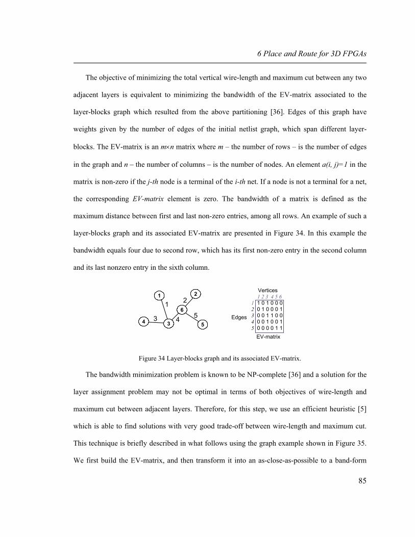
6 Place and Route for 3D FPGAs
85
The objective of minimizing the total vertical wire-length and maximum cut between any two
adjacent layers is equivalent to minimizing the bandwidth of the EV-matrix associated to the
layer-blocks graph which resulted from the above partitioning [36]. Edges of this graph have
weights given by the number of edges of the initial netlist graph, which span different layer-
blocks. The EV-matrix is an m×n matrix where m – the number of rows – is the number of edges
in the graph and n – the number of columns – is the number of nodes. An element a(i, j)=1 in the
matrix is non-zero if the j-th node is a terminal of the i-th net. If a node is not a terminal for a net,
the corresponding EV-matrix element is zero. The bandwidth of a matrix is defined as the
maximum distance between first and last non-zero entries, among all rows. An example of such a
layer-blocks graph and its associated EV-matrix are presented in Figure 34. In this example the
bandwidth equals four due to second row, which has its first non-zero entry in the second column
and its last nonzero entry in the sixth column.
21
6
34 5
1 2
3 4 5
Vertices
Edges
1 2 3 4 5 6 1 1 0 1 0 0 0 2 0 1 0 0 0 1 3 0 0 1 1 0 0 4 0 0 1 0 0 1 5 0 0 0 0 1 1
EV-matrix
Figure 34 Layer-blocks graph and its associated EV-matrix.
The bandwidth minimization problem is known to be NP-complete [36] and a solution for the
layer assignment problem may not be optimal in terms of both objectives of wire-length and
maximum cut between adjacent layers. Therefore, for this step, we use an efficient heuristic [5]
which is able to find solutions with very good trade-off between wire-length and maximum cut.
This technique is briefly described in what follows using the graph example shown in Figure 35.
We first build the EV-matrix, and then transform it into an as-close-as-possible to a band-form

6 Place and Route for 3D FPGAs
86
matrix. This problem is denoted as B(EV-matrix)-min problem (i.e., minimization of the
bandwidth of the EV-matrix problem). The procedure to solve this problem uses row and column
flips in order to sort rows and columns such that non-zero elements are moved towards the main
diagonal. For example, for the matrix shown in Figure 35, in order to “drift” non-zero elements
from the upper half towards the main diagonal (i.e., from right to left) column flips are performed
between columns 2 and 3 and then between column 6 is moved between columns 3 and 4. This
technique is performed to move non-zero elements from left to right and from top to bottom (for
the upper right half) and from left to right and from bottom to top (for the lower left half). When
the above procedure finishes, the example from Figure 34 becomes as described in Figure 35. The
goal of getting the matrix to a band-form (which translates into a best linear ordering) serves two
objectives:
1. Cutsize minimization – by having all 1’s in the matrix clustered along the main diagonal,
the cutsize (the number of nets cut by a vertical cut applied between any two consecutive nodes in
the linear arrangement) is minimized everywhere in the linear arrangement.
2. WL minimization – by minimizing the bandwidth (maximum distance spanned by any of
the nets) of the EV-matrix, the total wire-length of all nets is minimized.
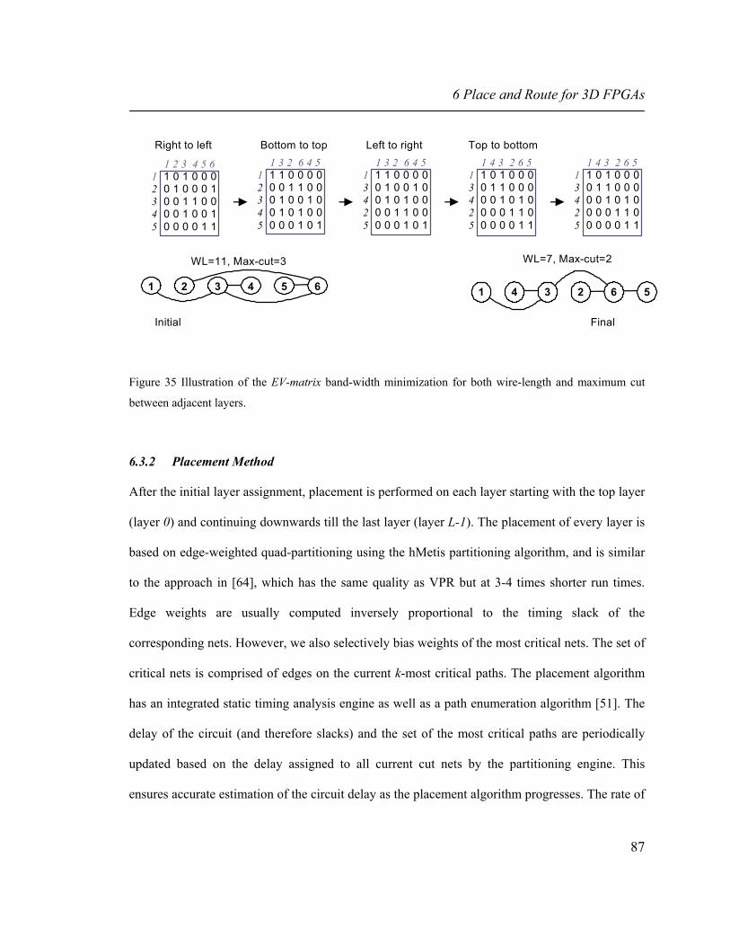
6 Place and Route for 3D FPGAs
87
1 2 3 4 5 6 1 1 0 1 0 0 0 2 0 1 0 0 0 1 3 0 0 1 1 0 0 4 0 0 1 0 0 1 5 0 0 0 0 1 1
2 1 63 4 5
WL=11, Max-cut=3
4 1 5 3 2 6
WL=7, Max-cut=2
1 3 2 6 4 5 1 1 1 0 0 0 0 2 0 0 1 1 0 0 3 0 1 0 0 1 0 4 0 1 0 1 0 0 5 0 0 0 1 0 1
Right to left 1 3 2 6 4 5 1 1 1 0 0 0 0 3 0 1 0 0 1 0 4 0 1 0 1 0 0 2 0 0 1 1 0 0 5 0 0 0 1 0 1
Bottom to top 1 4 3 2 6 5 1 1 0 1 0 0 0 3 0 1 1 0 0 0 4 0 0 1 0 1 0 2 0 0 0 1 1 0 5 0 0 0 0 1 1
Left to right 1 4 3 2 6 5 1 1 0 1 0 0 0 3 0 1 1 0 0 0 4 0 0 1 0 1 0 2 0 0 0 1 1 0 5 0 0 0 0 1 1
Top to bottom
Initial Final
Figure 35 Illustration of the EV-matrix band-width minimization for both wire-length and maximum cut
between adjacent layers.
6.3.2 Placement Method
After the initial layer assignment, placement is performed on each layer starting with the top layer
(layer 0) and continuing downwards till the last layer (layer L-1). The placement of every layer is
based on edge-weighted quad-partitioning using the hMetis partitioning algorithm, and is similar
to the approach in [64], which has the same quality as VPR but at 3-4 times shorter run times.
Edge weights are usually computed inversely proportional to the timing slack of the
corresponding nets. However, we also selectively bias weights of the most critical nets. The set of
critical nets is comprised of edges on the current k-most critical paths. The placement algorithm
has an integrated static timing analysis engine as well as a path enumeration algorithm [51]. The
delay of the circuit (and therefore slacks) and the set of the most critical paths are periodically
updated based on the delay assigned to all current cut nets by the partitioning engine. This
ensures accurate estimation of the circuit delay as the placement algorithm progresses. The rate of
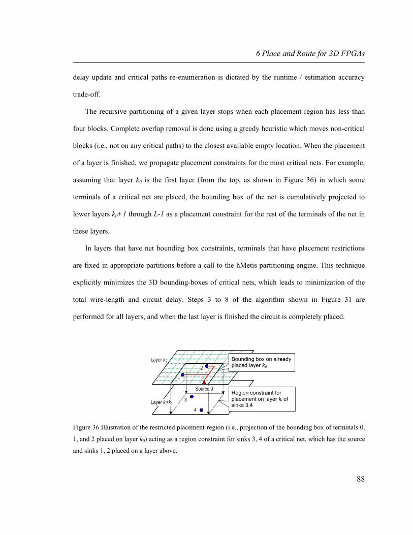
6 Place and Route for 3D FPGAs
88
delay update and critical paths re-enumeration is dictated by the runtime / estimation accuracy
trade-off.
The recursive partitioning of a given layer stops when each placement region has less than
four blocks. Complete overlap removal is done using a greedy heuristic which moves non-critical
blocks (i.e., not on any critical paths) to the closest available empty location. When the placement
of a layer is finished, we propagate placement constraints for the most critical nets. For example,
assuming that layer k0 is the first layer (from the top, as shown in Figure 36) in which some
terminals of a critical net are placed, the bounding box of the net is cumulatively projected to
lower layers k0+1 through L-1 as a placement constraint for the rest of the terminals of the net in
these layers.
In layers that have net bounding box constraints, terminals that have placement restrictions
are fixed in appropriate partitions before a call to the hMetis partitioning engine. This technique
explicitly minimizes the 3D bounding-boxes of critical nets, which leads to minimization of the
total wire-length and circuit delay. Steps 3 to 8 of the algorithm shown in Figure 31 are
performed for all layers, and when the last layer is finished the circuit is completely placed.
Bounding box on already placed layer k0
Region constraint for placement on layer ki of sinks 3,4
Source 0 1
2
3
4
Layer k0
Layer ki>k0
Figure 36 Illustration of the restricted placement-region (i.e., projection of the bounding box of terminals 0,
1, and 2 placed on layer k0) acting as a region constraint for sinks 3, 4 of a critical net, which has the source
and sinks 1, 2 placed on a layer above.

6 Place and Route for 3D FPGAs
89
6.4 Routing Algorithm
6.4.1 Description of Detailed Routing Algorithm
The 3D FPGA architecture (see Figure 37) – described in the architecture file – is represented as
a routing resource graph. Each node of the routing resource graph represents a wire (horizontal
tracks in the x and y channels of all layers and vertical vias in the z channels) or a logic block (i.e.,
CLB) input or output pin. A directed edge represents a unidirectional switch (such as a tri-state
buffer). A pair of directed edges represents a bi-directional switch (such as a pass transistor). An
example of a routing resource graph construction is shown in Figure 38.
Figure 37 Illustration of key elements of a 3D architecture; routing resources are horizontal tracks and
vertical vias.
3D switch-box
Horizontal tracks
Vertical vias
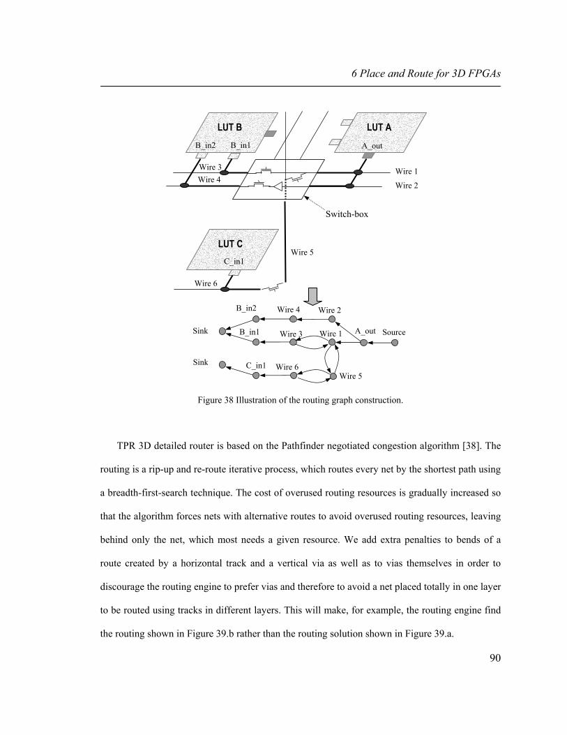
6 Place and Route for 3D FPGAs
90
Figure 38 Illustration of the routing graph construction.
TPR 3D detailed router is based on the Pathfinder negotiated congestion algorithm [38]. The
routing is a rip-up and re-route iterative process, which routes every net by the shortest path using
a breadth-first-search technique. The cost of overused routing resources is gradually increased so
that the algorithm forces nets with alternative routes to avoid overused routing resources, leaving
behind only the net, which most needs a given resource. We add extra penalties to bends of a
route created by a horizontal track and a vertical via as well as to vias themselves in order to
discourage the routing engine to prefer vias and therefore to avoid a net placed totally in one layer
to be routed using tracks in different layers. This will make, for example, the routing engine find
the routing shown in Figure 39.b rather than the routing solution shown in Figure 39.a.
Source A_out Wire 1Wire 3B_in1
B_in2
Sink
Wire 2Wire 4
Wire 5Wire 6Sink C_in1
LUT A LUT B B_in1 B_in2 A_out
LUT C C_in1
Wire 2
Wire 1 Wire 4 Wire 3
Wire 6
Wire 5
Switch-box
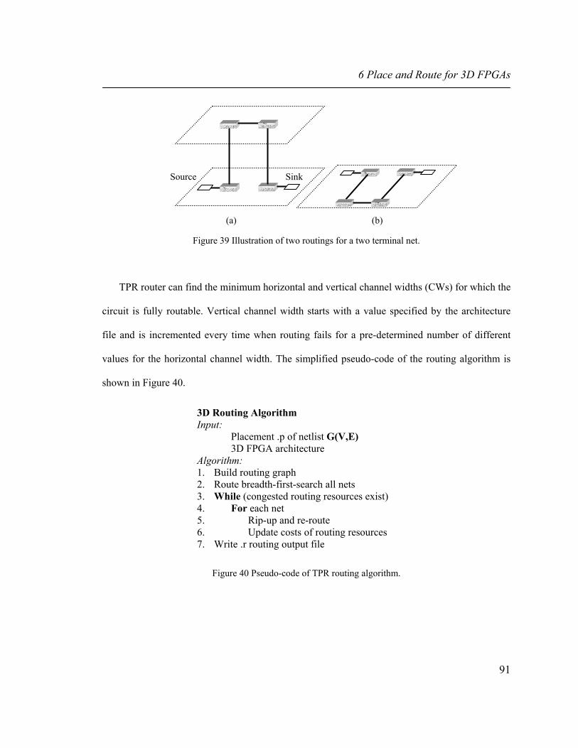
6 Place and Route for 3D FPGAs
91
Figure 39 Illustration of two routings for a two terminal net.
TPR router can find the minimum horizontal and vertical channel widths (CWs) for which the
circuit is fully routable. Vertical channel width starts with a value specified by the architecture
file and is incremented every time when routing fails for a pre-determined number of different
values for the horizontal channel width. The simplified pseudo-code of the routing algorithm is
shown in Figure 40.
3D Routing Algorithm Input: Placement .p of netlist G(V,E) 3D FPGA architecture Algorithm: 1. Build routing graph 2. Route breadth-first-search all nets 3. While (congested routing resources exist) 4. For each net 5. Rip-up and re-route 6. Update costs of routing resources 7. Write .r routing output file
Figure 40 Pseudo-code of TPR routing algorithm.
(a)
Source Sink
(b)
6 Place and Route for 3D FPGAs
92
6.4.2 Computation of Total and Foot-print Area
In order to be able to compute the foot-print chip area after detailed routing is completed for 3D
architectures (simulations results reported in Section 6) we use a new formula, which is the
adaptation to 3D of the computations performed in 2D. Footprint area is calculated as total area
divided by number of layers. Generally, the overall chip area is the summation of the area taken
by logic (CLBs) and routing resources (switch boxes, connection boxes, track segments).
RoutingLogic AreaAreaArea += (4)
The above formula reduces to the following simplified equation (we omitted details for
brevity), for 2D case (see [19], pages 207-217):
2212 )]([ WHCWAreaCHCWCAreaArea muxLUTD ⋅⋅+⋅+= (5)
where:
22)(log6)( 2 −+⋅= HCWHCWHCWAreamux (6)
represents the area of all minimum-width transistors required by a multiplexer with HCW
inputs [19]. Such multiplexers are used to connect tracks in the routing channels to the input pins
of CLBs and because of that we need multiplexers with a number of inputs equal to the horizontal
channel with, HCW. C1, C2 are functions of track-buffer area, number of input pins within an
FPGA tile, number of input pins within a tile which share a common buffer, output pin buffer
area, number of pass transistors corresponding to an output pin of a CLB, buffer (inside switch
boxes) area, and Fs (Fs=3 for 2D) [19]. AreaLUT is the total area of a CLB, which may contain one
or more LUTs. W is the width of the FPGA chip measured as multiple of inter-CLB distances
(assumed to be equal to the height of the FPGA chip).
The overall chip area computation, extended to 3D case, is given by the following expression:

6 Place and Route for 3D FPGAs
93
233..
222..
2.......
2
3..2...
)1(),,(
)1(),,(
),,,,,_(
−⋅⋅+
−⋅⋅−+
⋅⋅+⋅⋅=
+++=
+=
WLVCWAreaFArea
WLVCWHCWAreaFArea
WLAreaHCWAreaAreaAreaipinNumAreaWLArea
AreaAreaAreaAreaAreaAreaArea
BuffD
sDBoxSwitch
BuffD
sDBoxSwitch
TransPassmuxOpinBuffTrackIpinBuffTrackTileBoxConTileLUT
DBoxSwitchDBoxSwitchBoxConLogic
RoutingLogic
(7)
which can be written in a simpler form as:
243
22
'13
)1(])([)]([
−⋅⋅⋅+−⋅+⋅⋅⋅+⋅+=
WLVCWCVCWHCWCWLHCWAreaCHCWCAreaArea muxLUTD (8)
432'1 ,,, CCCC are functions of track-buffer area, AreaTrack.Buff for input or output pins of a CLB,
number of input pins within an FPGA tile, Num_ipinTile, number of input pins within a tile which
share a common buffer, area of all pass transistors corresponding to an output pin of a CLB,
AreaPass.Trans, buffer (inside switch boxes) area, AreaBuff, and Fs (Fs=3 for 2D and Fs=6 for 3D).
HCW, VCW are horizontal and vertical channel widths. L is number of layers for 3D
architectures. In the formulas above, AreaSwitch.Box.2D and AreaSwitch.Box.3D represent switch-box area
fractions corresponding to connections of tracks characterized by Fs=3 (horizontal tracks entering
a switch-box connect to only other horizontal tracks) and of tracks characterized by Fs=6
(horizontal tracks entering a switch-box connect to both horizontal and vertical tracks). Because
number of vertical tracks for a z channel is always smaller than the number of horizontal tracks in
x, y channels we have to consider the difference HCW-VCW.
6.5 Simulation Results
6.5.1 3D Architectures
Our goal is to study the variation of the circuit delay and the total wire-length as a function of the
number of layers when the delay of an inter-layer wire (i.e., vertical via) has different values. We

6 Place and Route for 3D FPGAs
94
considered two different architectures: Sing-Seg and Multi-Seg (see Figure 41). In both
architectures, each horizontal layer has a routing architecture that resembles the Xilinx Virtex II
architecture (they have wire segments of lengths 1, 2, and 6, as well as long lines in each layer).
However, Sing-Seg has vertical (inter-layer) vias of length one only, while Multi-Seg has vertical
vias that span 1, 2, and all planes. Length one vertical segment is assumed to have the same delay
and wire-length as 2D unit-length segments. This is a reasonable assumption, because 3D
fabrication methods such as [74] can create inter-layer vias that are merely 5-10µm long. In such
vertical segments, the switch delay dominates the delay of the segment, which is similar to the 2D
case. Our architectures have one 4-input LUT per CLB as this is a common assumption made in
most previous works. We do not include a description of the LUT because it is essentially the
same as for 2D cases and there are many previous works describing them such as [19]. Vertically,
our architectures are unique by being vertical in the third dimension, but they are also along the
same line of traditional FPGAs: either containing vias of length one or vias spanning more layers.
The switch-box in our architecture is different from the 2D case by the fact that some tracks are
connecting to the vertical vias. The switch-box will be described more later on (see Figure 48).
We would like to mention that these architectures are very complex and our implementation is
very flexible supporting any combination of segment and via lengths as well as any known type
of switch-box. We randomly placed IO terminals on the periphery of every layer after the
partitioning and assignment to layers is performed. However, the user can provide locations for
IO terminals.

6 Place and Route for 3D FPGAs
95
Figure 41 Two different architectures used for simulations: Sing-Seg and Multi-Seg.
6.5.2 Delay Results of TPR
We cannot compare our results to any of the previous works for a couple of reasons. First, our
place and route tool is the first to report comprehensive results on wire-length and circuit delay as
well as on all other metrics such as chip area, horizontal and vertical channel widths, and run-
times on all twenty circuit benchmarks of the VPR package. We cannot compare to the only
previous existing results reported in [11] or [55] because the authors of [11] used only six circuit
benchmarks (unavailable to us) different (except Apex2) from those we use. Moreover, the
authors of [11] report only wire-length and minimum channel width results obtained for a very
simple architecture, which only contains horizontal and vertical routing segments of length one.
This is in contrast with our architectures, which have mixed – Virtex II-like – routing resources
both horizontally and vertically. The authors of [11] use only four layers whereas we report
results for a range between two and ten layers. The authors of [55] report results for wire-length
only for a number of layers between two and four, using unknown circuit benchmarks and
architecture, most likely similar to the one used in [11] and different from our more complex
architectures. Since we are providing the source code and benchmarks that we use in this paper
on the World Wide Web (see the Summary Section), other researchers can easily compare their
Switch-box
LUT
Multi-Seg: Length 1, 2 and long vias CWz = 6
Sing-Seg: Length 1 vias only CWz = 6

6 Place and Route for 3D FPGAs
96
results to ours. Nevertheless, we present and discuss, for comparison purposes, results obtained
with a simulated annealing placement algorithm SA-TPR, which was developed as a direct
extension of VPR placement algorithm to the 3D case [68]. Placements obtained using SA-TPR
were routed using our 3D routing algorithm.
We placed and detailed routed all circuits (see Table 6) on a number of layers varied between
one (the 2D case) and ten. We recorded the average circuit delay and the average total wire-
length of four different runs for each circuit. TPR results showing post-routing delay for both
routing architectures are presented in Figure 42 and Figure 43. In Figure 42, circles represent the
average delay of all circuits and squares represent the minimum and the maximum delays among
all circuits. The comparison between the variation of the average delay values obtained using
partitioning-based (TPR) and SA-based (SA-TPR) placement algorithms is illustrated in Figure
44. We observe that delay decreases13 by about 30% for both architectures using either placement
algorithm compared to the 2D case, although architecture Multi-Seg shows slightly better delays,
as the number of layers increases beyond six. However, the difference is not large, mainly
because the routing algorithm considers fully buffered14 routing resources, which leads to
comparable delay values for both architectures. Delay achieved using the SA-based placement
algorithm is smaller compared to the delay achieved using the partitioning-based placement
algorithm, which is not surprising, because annealing takes longer runtimes.
13 We notice that delay does not decrease as much when compared to results reported for ASICs by other
researchers. This emphasizes the intrinsic higher complexity of FPGAs and their hyper-dimensional routing
architectures in which a LUT has more “immediate” neighbors through different segment lengths. 14 Modern FPGAs use fully buffered routing resources extensively.

6 Place and Route for 3D FPGAs
97
Del
ey a
fter r
outin
g [s
]
Del
ey a
fter r
outin
g [s
]
Number of layers Number of layers
Figure 42 Circuit delay after detailed routing as a function of number of layers for both architectures: Sing-
Seg (left) and Multi-Seg (right).
Del
ey a
fter r
outin
g [s
]
Number of layers
Del
ey a
fter r
outin
g [s
]
Number of layers
Figure 43 Actual circuit delay variations for both architectures: Sing-Seg (left) and Multi-Seg (right). TPR
is used for placement.

6 Place and Route for 3D FPGAs
98
Del
ey a
fter r
outin
g [s
]
Number of layers
Figure 44 Variation of delay as reported after detailed routing for placements obtained using our TPR and
SA-TPR of [68].
We noticed that the amount of delay decrease compared to the 2D case for different circuits
and same number of layers can vary. For example, delay decreases (Figure 43) by 27% for Pdc
benchmark but only 18% for Spla benchmark when nine layers are used. We suspect this is due to
the internal structure (such as higher connectivity) of Pdc as opposed to Spla, which leads to a
larger fraction of nets spanning different numbers of layers, as shown in Figure 45. During our
experiments we also noticed that benchmarks with large number of terminals (relative to the
number of cells), such as Des (see Table 6), tend to lead to more delay decrease compared to 2D
case. This can be explained by the fact that in the 2D case, the chip size necessary to
accommodate all terminals is bigger than if the circuit had less terminals (i.e., final chip will have
more “white-space”) and therefore delays of nets involving input or output terminals will have
larger routing delays in 2D case.

6 Place and Route for 3D FPGAs
99
00.0050.01
0.0150.02
0.0250.03
0.0350.04
0.045
2 3 4 5 6 7 8 9
Number diff layers: n
Frac
tion
num
ber o
f net
s w
ith te
rmin
als
in n
diff
la
yers
SplaPdc
Figure 45 Fraction (relative to number of nets with terminals in only one layer) of nets with terminals in n
different layers for two circuit-benchmarks.
6.5.3 Wire Length Results of TPR
Wire-length results of TPR on Multi-Seg architecture are shown in Figure 46. Results for
architecture Sing-Seg and using the SA-based placement algorithm are similar. Figure 47, shows
the average wire length for architecture Multi-Seg as the number of layers increases. We observe
that wire-length after detailed routing decreases by 25% on average as the number of layers
increases. If the length of the inter-layer via increases, then the total wire-length decrease will be
less. That is mainly because the fraction of the vertical wire-length relative to the total wire-
length will become significant and also the average net delay will increase due to bending (i.e.,
switches) of nets spanning more layers. Wire-length achieved using the SA-based placement
algorithm is smaller compared to the wire-length achieved using the partitioning-based placement
algorithm.

6 Place and Route for 3D FPGAs
100
Wire
leng
th a
fter r
outin
g / 2
D
Number of layers
Figure 46 Variation of wire-length, normalized to 2D case, as reported after detailed routing. TPR is used
for placement.
Ave
rage
wire
leng
th
Number of layers
Figure 47 Variation of average wire-length after detailed routing as a function of number of layers, using
both TPR and SA-TPR [68] placement algorithms.
We note that the decrease in total wire-length can have favorable impact on the routing
congestion (hence channel width), as well as power dissipation (especially due to the fact that

6 Place and Route for 3D FPGAs
101
most of the power dissipated in FPGAs is due to interconnects, which account for more than 80%
of the total area) as predicted by Rahman et al. in [73].
The decrease in total WL is directly related to a decrease of the average net wire-length,
which in turn relates to the overall usage of routing resources and therefore to the circuit delay.
Variations of the average net wire-length, and other metrics of interest, are shown in Figure 49
(see also Table 7 and Table 8). Routing area counts the exact number of pass transistor and
SRAM cells that control them, as suggested in [19]. We observe that overall area (i.e., chip foot-
print area multiplied by the number of layers) slightly increases for a small number of layers. This
increase is due to the higher connectivity inside of a switch box (i.e., a track entering a 3D switch
box will have to connect to 5 correspondents as opposed to only 3 in the 2D case; see Figure 48).
However, routing area decreases as the number of layers increases for Multi-Seg architecture, as a
direct consequence of a decrease of the horizontal channel width (HCW) required for successful
routing (Figure 49). Routing area increase is overall less than 10% when SA-based placement
algorithm is used. Except for cases where only few layers are used, CW decreases significantly.
The reason is that the number of vertical connections is minimized. In other words, the
partitioning algorithm is able to find the clustering structure of the circuit and practically divide
the initial netlist into a number of smaller circuits with similar internal structure (in terms of
connectivity or Rent’s parameter) to the initial one. As a consequence, the horizontal channel
width for each layer will be in the same range as when the initial netlist is placed in 2D.

6 Place and Route for 3D FPGAs
102
Figure 48 Third dimension adds vertical tracks which require five connections.
We observe that, overall, run-times of SA-based placement are about twice the run-times of
detailed routing (see Table 6) and about an order of magnitude longer than run-times of
partitioning-based placement. Therefore, partitioning-based placement can be used for efficient
solution space (especially for big circuits) and different architectural assumptions exploration.
Also, the vertical channel widths reported in Table 6 are 1/5 of the horizontal channel widths,
which demonstrates that our layer partitioning and linear placement as well as the routing
algorithm are very well tuned to minimize the use of vertical tracks. Another advantage of using
fewer vertical tracks greatly reduces the required area for switchboxes (A vertical/horizontal
intersection with Fs=3 requires 6 switches, while an intersection with Fs=5 requires 15 switches.
Each switch has a pass transistor, an SRAM cell, and possibly a buffer.).
2D Switch-box 3D Switch-box
Fs=3
Fs=5
Fs=3
Fs=3
Fs=5 Fs=3
Fs=3
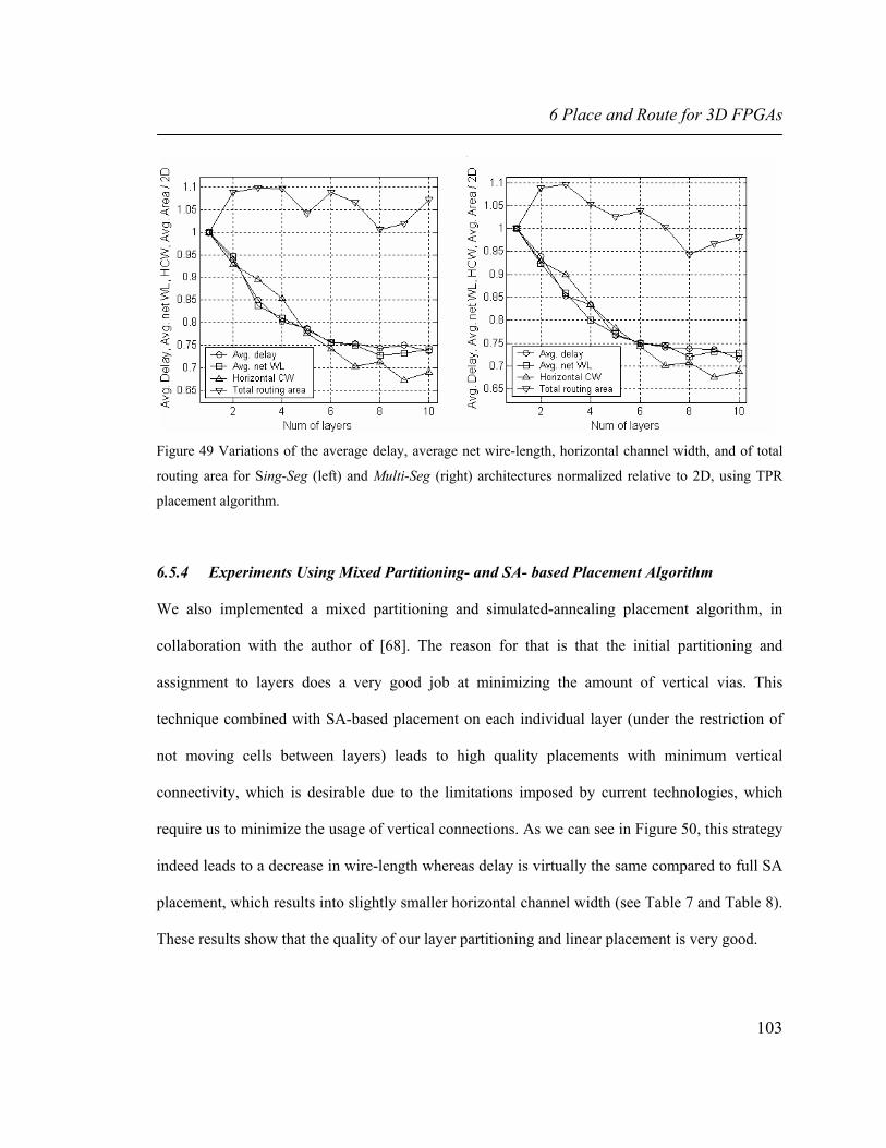
6 Place and Route for 3D FPGAs
103
Figure 49 Variations of the average delay, average net wire-length, horizontal channel width, and of total
routing area for Sing-Seg (left) and Multi-Seg (right) architectures normalized relative to 2D, using TPR
placement algorithm.
6.5.4 Experiments Using Mixed Partitioning- and SA- based Placement Algorithm
We also implemented a mixed partitioning and simulated-annealing placement algorithm, in
collaboration with the author of [68]. The reason for that is that the initial partitioning and
assignment to layers does a very good job at minimizing the amount of vertical vias. This
technique combined with SA-based placement on each individual layer (under the restriction of
not moving cells between layers) leads to high quality placements with minimum vertical
connectivity, which is desirable due to the limitations imposed by current technologies, which
require us to minimize the usage of vertical connections. As we can see in Figure 50, this strategy
indeed leads to a decrease in wire-length whereas delay is virtually the same compared to full SA
placement, which results into slightly smaller horizontal channel width (see Table 7 and Table 8).
These results show that the quality of our layer partitioning and linear placement is very good.

6 Place and Route for 3D FPGAs
104
Ave
rage
wire
leng
th
Number of layers Number of layers
Del
ay [s
]
Figure 50 Variation of average wire-length as estimated after placement and as reported after detailed
routing, using partitioning-, SA-, and mixed partitioning + SA- based placement algorithms (left) and
variation of delay as reported after detailed routing (right).
Table 6 Simulated circuits: statistics, vertical channel width (VCW) for successful routing, and run-time
(TPR compiled with g++ on a Linux box running on a Xeon 2.54GHz with 2G of memory).
VCW CPU (s)
Circuit No. CLBs No. IOs TPR SA- TPR [68]
Par-based placement
SA-based Placement [68]
Detailed Routing
Ex5p 1064 71 6 5 7 85 77 Apex4 1262 28 6 5 8 105 76 Misex3 1397 28 6 5 9 55 84 Alu4 1522 22 5 5 16 145 61 Des 1591 501 5 5 11 227 69 Seq 1750 76 5 5 12 212 114 Apex2 1878 42 5 5 13 243 148 Spla 3690 62 5 6 37 912 532 Pdc 4575 56 7 7 60 1354 1039 Ex1010 4598 20 4 5 56 1238 273 Dsip 1370 426 5 5 28 154 34 Tseng 1407 174 5 5 8 70 14 Diffeq 1497 103 5 5 14 154 46 Bigkey 1707 426 5 5 22 209 48 S298 1931 10 5 5 23 208 53 Frisc 3556 136 5 5 56 881 227 Elliptic 3604 245 5 5 74 818 142 S38417 6406 135 5 5 133 2000 210 S38584.1 6447 342 5 5 230 2034 268 Clma 8383 144 5 5 199 892 950 Sum 1016 11996 4465

6 Place and Route for 3D FPGAs
105
Table 7 Average (of all circuits) of Delay, wire-length (WL), horizontal channel width (HCW), and routing
area after successful routing for Sing-Seg architecture.
TPR SA-TPR [68] Combined Partitioning + SA Place Num
layers Delay (× 10-7) WL Routing
area HCW Delay (× 10-7) WL Routing
area HCW Delay (× 10-7) WL Routing
area HCW
1 1.62 107087 1.00 1.00 1.30 79553 1.00 1.00 1.27 79626 1.00 1.00 2 1.52 98808 1.088 0.92 1.22 76072 1.016 0.95 1.18 73663 1.113 0.99 3 1.37 93162 1.097 0.89 1.18 74786 1.096 0.96 1.13 69913 1.114 0.90 4 1.30 87410 1.096 0.85 1.12 73277 1.091 0.93 1.10 67746 1.108 0.85 5 1.28 84741 1.041 0.77 1.08 71817 1.117 0.93 1.06 68154 1.119 0.85 6 1.22 81707 1.089 0.74 1.06 70975 1.106 0.91 1.05 67045 1.121 0.81 7 1.22 80143 1.065 0.70 1.05 69902 1.116 0.89 1.03 65753 1.119 0.78 8 1.20 78589 1.005 0.71 1.03 69589 1.096 0.87 1.01 67361 1.117 0.80 9 1.21 78456 1.018 0.67 1.04 68800 1.100 0.87 1.04 66559 1.117 0.77 10 1.19 78643 1.072 0.69 1.01 68411 1.084 0.85 1.02 66185 1.122 0.77
Table 8 Average (of all circuits) of Delay, wire-length (WL), horizontal channel width (HCW), and routing
area after successful routing for Multi-Seg architecture.
TPR SA-TPR [68] Combined Partitioning + SA Place Num
layers Delay (× 10-7) WL Routing
area HCW Delay (× 10-7) WL Routing
area HCW Delay (× 10-7) WL Routing
area HCW
1 1.62 107087 1.000 1.00 1.28 79410 1.000 1.00 1.27 79626 1.000 1.00 2 1.52 98808 1.088 0.92 1.20 76088 1.015 0.96 1.18 73663 1.113 0.99 3 1.38 93162 1.096 0.89 1.19 75304 1.068 0.96 1.14 70729 1.112 0.91 4 1.35 87410 1.053 0.83 1.12 73796 1.075 0.95 1.07 67383 1.107 0.86 5 1.24 84741 1.025 0.78 1.07 72228 1.045 0.90 1.06 66798 1.113 0.82 6 1.21 81707 1.038 0.74 1.03 70888 1.064 0.90 1.05 66682 1.115 0.80 7 1.20 80143 1.003 0.70 1.03 70710 1.052 0.88 1.03 65605 1.115 0.77 8 1.19 78589 0.942 0.70 1.02 69849 1.054 0.87 0.98 67049 1.113 0.81 9 1.19 78456 0.967 0.67 0.98 69190 1.062 0.87 0.98 65536 1.114 0.77 10 1.16 78643 0.981 0.68 0.97 68840 1.058 0.85 0.98 65439 1.115 0.77

6 Place and Route for 3D FPGAs
106
6.6 Summary
Benefits which 3D FPGA integration can offer were analyzed using a new placement and detailed
routing tool. The partitioning-based placement algorithm has integrated techniques for
minimization of the 3D bounding-boxes of nets and of the delays of the critical paths. Simulation
experiments, after detailed routing, showed potential total decrease of 25% for wire-length and
35% for delay. We observed that the Multi-Seg architecture shows slightly better delay
characteristics compared to the Sing-Seg architecture.
We plan to analyze whether circuits are fully routable when vertical channels do not exist at
every CLB location. The reason for that is because a smaller (i.e., rare) number of vertical vias is
preferred due to technological limitations and because an architecture with a smaller number of
vias translates into a smaller chip foot-print area (due to smaller transistor area dedicated to
connections inside switch boxes). Source code and documentation is available for download at:
http://www.ece.umn.edu/users/kia/.

7 Conclusions and Future Work
107
7 Conclusions and Future Work
7.1 Dissertation Summary
The increase in circuit complexities and the high demand for short time-to-market products force
designers to adopt divide-and-conquer design techniques. Furthermore, ever-growing
performance expectations require designers to perform optimization at all levels of the design
cycle. In the first part of this dissertation (Chapters 3 and 4), we addressed the problem of delay
optimization at the physical design stage. A new net-based statistical timing-driven partitioning
algorithm demonstrated that circuit delay could be improved whereas the run-time remained
virtually the same with insignificant cutsize deterioration. We also proposed a path-based multi-
objective partitioning for cutsize and circuit delay minimization. We changed the partitioning
process itself by introducing a new objective function that incorporates a truly path-based delay
component for the most critical paths. Integration of the proposed partitioning algorithms into a
placement tool demonstrated the ability of the proposed edge-weighting and path-based
approaches for partitioning to lead to a better circuit performance.
Due to the non-uniform scaling of transistors and interconnects, previously ignored
perturbations have become major design challenges because of their significant negative impact
on the predictability of classic design methodologies, as well as on performance. In the second
part of this dissertation (Chapter 5) we proposed new physical synthesis design techniques, which
shall lead to more robust designs and more predictable design methodologies. More specifically,

7 Conclusions and Future Work
108
we proposed and developed means for changing a standard timing-driven partitioning-based
placement algorithm in order to design more predictable and robust circuits without sacrificing
much of performance.
Due to technology scaling global wires dominate the delay and power budgets, and signal
integrity, IR-drops, and process variations pose new design problems. In response to these
problems, 3D integration could significantly reduce wire-lengths, boost yield, and could
particularly be useful for FPGA fabrics because it could address problems related to routing
congestion, limited I/O connections, and long wire delays. Practical application of 3D integrated
circuits yet needs to gain momentum, partly due to a lack of efficient 3D CAD tools. In the third
part of this dissertation (Chapter 6) we proposed a new efficient timing-driven partitioning-based
placement and detailed routing tool for 3D FPGA integration. We showed that 3D integration
could result in smaller circuit delay and wire-length.
7.2 Future Work
This work represents a step further towards developing physical design techniques capable to
cope with the new and more difficult problems of the ever increasing circuit (both VLSI circuits
and FPGAs) complexities. The ideas presented in this dissertation can be seen as triggers of some
avenues of future work, which are discussed in the following sub-sections.
7.2.1 Multi-objective Optimization
There is still much to do on multi-objective optimization. Multi-objective optimization is more
difficult than single objective optimization (e.g., mincut partitioning or wirelength-driven
placement) because often intricate trade-offs between objectives exist. This means that it is very
likely that a single solution will not be optimum with respect to every objective, and therefore one

7 Conclusions and Future Work
109
will have to first understand the mechanisms behind these trade-offs (influenced by the accuracy
of the models too) and then device design techniques to exploit and account for these
mechanisms, which shall lead to the best solution from all perspectives while satisfying all the
initial design constraints. In Chapter 4 of this dissertation, we presented a solution to multi-
objective (cutsize and delay) partitioning, and we embedded our partitioning algorithm into a
placement tool. The multi-objective design approach can be extended to directly incorporate other
objectives (such as power) into the cost function or be applied at other design flow levels such as
logic synthesis. Better, more accurate models (e.g., delay, power models) yet efficient (i.e., which
shall not add too much run-time overhead) will contribute to obtaining additional results,
preferably using industry size benchmark circuits.
7.2.2 Robust Design under Uncertainty
Rampant decreasing of transistor and feature size as technology advances into deep submicron
(DSM) geometries gave rise to many new challenging problems (IR drops, parameter variations,
crosstalk, etc.). Many of these problems are due to process variations, temperature, and supply
voltage changes, which cause the emergence of uncertainty in almost every design aspect. The
ideas presented in Chapter 5 represent an effort in trying to cope with the difficulties associated
with the DSM technologies. Much work will have to be done in the recently awaken domain of
probabilistic and “for manufacturing” design in order to develop design methodologies which
shall be more predictable (predictability is to be achieved in the face of design uncertainties) and
robust (high robustness means that performance of the design is less influenced by noise factors
and remains within acceptable limits).

7 Conclusions and Future Work
110
7.2.3 Architectural Studies and Efficient CAD Support for 2D and 3D FPGAs
New FPGA architectures cannot be proposed and studied independently. An important
component of that process is represented by the CAD tools and their algorithms used to design
circuits of ever increasing size. Much work is still needed in finding better FPGA architectures (in
terms of performance, power, area, etc.) to make them more competitive relative to standard cell
designs. 3D FPGA architectures (discussed in Chapter 6) can represent (apart from
nanotechnology) a potential new Moore’s law enabler. However, more architectural studies on
problems regarding for example the distribution of vertical vias and their lengths or the presence
of blockages (under the form of heat pipes or macro-blocks such as processors or other DSP
blocks embedded into the reconfigurable fabric) need to be investigated. Likewise, efficient
scalable algorithms will have to be developed in order to facilitate the analysis of architectures as
well as the design automation process.

Bibliography
111
Bibliography
[1] C. Ababei, N. Selvakkumaran, K. Bazargan, and G. Karypis, “Multi-objective Circuit
Partitioning for Cutsize and Path-based Delay Minimization“, Proc. IEEE/ACM
International Conference on Computer Aided Design (ICCAD), 2002, pp. 181-185.
[2] C. Ababei, N. Selvakkumaran, K. Bazargan, G. Karypis, “Multi-objective Circuit
Partitioning for Cutsize and Path-based Delay Minimization”, Submitted to ACM
Transactions on Design Automation of Electronic Systems.
[3] C. Ababei and K. Bazargan, “Timing Minimization by Statistical Timing hMetis-based
Partitioning“, International Conference on VLSI Design, 2003, pp. 58-63.
[4] C. Ababei and K. Bazargan, “Placement Method Targeting Predictability Robustness and
Performance“, Proc. IEEE/ACM International Conference on Computer Aided Design,
2003, pp. 81-85.
[5] C. Ababei and K. Bazargan, “Non-contiguous Linear Placement for Reconfigurable
Fabrics”, Proc. Reconfigurable Architectures Workshop (RAW), 2004.
[6] C. Ababei, P. Maidee, and K. Bazargan, “Exploring Potential Benefits for 3D FPGA
Integration”, Proc. Field Programmable Logic and its Applications (FPL), 2004.
[7] C. Ababei, H. Mogal, and K. Bazargan, “Three-dimensional Place and Route for FPGAs”,
Proc. IEEE/ACM Asia and South Pacific Design Automation Conference (ASP-DAC),
2005.

Bibliography
112
[8] C. Ababei, H. Mogal, K. Bazargan, “Three-dimensional Place and route for 3D FPGAs”,
Submitted to IEEE Transactions on Computer Aided Design of Integrated Circuits and
Systems.
[9] A. Agarwal, D. Blaauw, V. Zolotov, and S. Vrudhula, “Statistical Timing Analysis using
Bounds”, Proc. IEEE/ACM Design, Automation and Test in Europe Conference, 2003, pp.
62-67.
[10] H. Ajami, K. Banerjee, M. Pedram, and L. van Ginneken, “Analysis of Non-Uniform
Temperature-Dependent Interconnect Performance in High Performance ICs”, Proc.
IEEE/ACM Design Automation Conference, 2001, pp. 567-572.
[11] A. J. Alexander, J. P. Cohoon, Jared L. Colflesh, J. Karro, and G. Robins, “Three-
Dimensional Field-Programmable Gate Arrays”, Proc. Intl. ASIC Conf., 1995, pp. 253-256.
[12] A. J. Alexander, J. P. Cohoon, Jared L. Colflesh, J. Karro, E. L. Peters, and G. Robins,
“Placement and Routing for Three-Dimensional FPGAs”, Fourth Canadian Workshop on
Field-Programmable Devices, May 1996, pp. 11-18.
[13] C. J. Alpert, D. J. Huang, A. B. Kahng, “Multilevel Circuit Partitioning”, Proc. IEEE/ACM
Design Automation Conference, 1997, pp. 530-533.
[14] X. Bai, C. Visweswariah, P. N. Strenski, and D. J. Hathaway, “Uncertainty-Aware Circuit
Optimization”, Proc. IEEE/ACM Design Automation Conference, 2002, pp. 58-63.
[15] K. Banerjee, S. J. Souri, P. Kapur, and K. C. Saraswat, “3-D ICs: A novel chip design for
improving deep submicron interconnect performance and systems-on-chip integration”,
Proceedings of the IEEE, Vol. 89, No. 5, May 2001, pp. 602-633.

Bibliography
113
[16] K. Bazargan, S. Kim, and M. Sarrafzadeh, “Nostradamus: A Floorplanner of Uncertain
Designs”, IEEE Transactions on Computer Aided Design of Integrated Circuits and
Systems, Vol. 18, No. 4, Apr. 1999, pp. 389-397.
[17] M. Berkelaar, “Statistical Delay Calculation, a Linear Time Method”, Proc. Int. Workshop
on Timing Issues in the Specification and Synthesis of Digital Systems (TAU), 1997, pp. 15-
24.
[18] V. Betz and J. Rose, “VPR: A New Packing Placement and Routing Tool for FPGA
Research”, Field-Programmable Logic App., 1997, pp. 213-222.
[19] V. Betz, J. Rose, and A. Marquardt, “Architecture and CAD for Deep-Submicron FPGAs”,
Kluwer Academic Publishers, 1999.
[20] G. Borriello, C. Ebeling, S. Hauck, and S. Burns, “The Triptych FPGA Architecture”, IEEE
Transactions on VLSI Systems, Vol. 3, No. 4, 1995, pp. 491-501.
[21] E. Bozorgzadeh, R. Kastner, and M. Sarrafzadeh, “Creating and Exploiting Flexibility in
Steiner Trees”, Proc. IEEE/ACM Design Automation Conference, 2001, pp. 195-198.
[22] J. Burns, L. McIlrath, J. Hopwood, C. Keast, D. P. Vu, K.Warner, and P. Wyatt, “An soi-
based three dimensional integrated circuit technology”, Proc. IEEE International SOI
Conference, Oct. 2000, pp. 20-21.
[23] M. Burnstein and R. Pelavin, “Hierarchical Wire Routing”, IEEE Transactions on
Computer Aided Design of Integrated Circuits and Systems, Vol. 2, No. 4, Oct. 1983, pp.
223-234.
[24] E. Caldwell, A. B. Kahng, and I. L. Markov, “Can Recursive Bisection Alone Produce
Routable Placements?”, Proc. IEEE/ACM Design Automation Conference, 2000, pp. 477-
482.

Bibliography
114
[25] U. V. Catalyurek and C. Aykanat, “Hypergraph-partitioning-based Decomposition for
Parallel Sparse-matrix vector Multiplication”, IEEE Transactions Parallel and Distributed
Systems, Vol. 10, No. 7, July 1999, pp. 673-693.
[26] Y. K. Cheng and S. M. Kang, “A Temperature-Aware Simulation Environment for Reliable
ULSI Chip Design”, IEEE Transactions on Computer Aided Design of Integrated Circuits
and Systems, Vol 19, No. 20, Oct. 2000.
[27] S. Chiricescu, “Parametric Analysis of a Dynamically Reconfigurable Three-Dimensional
FPGA”, Ph.D. Dissertation, Northeastern Univ., Boston, MA, Dec. 1999.
[28] S. Chiricescu, M. Leeser, and M. M. Vai, “Design and Analysis of a Dynamically
Reconfigurable Three-Dimensional FPGA”, IEEE Transactions on VLSI Systems, Vol. 9,
No. 1, Feb. 2001, pp. 186-196.
[29] J. Cong and C. Wu, “Global Clustering-Based Performance-Driven Circuit Partitioning”,
Proc. IEEE/ACM Int. Symposium on Physical Design (ISPD), 2002, pp. 149-154.
[30] J. Cong and S. K. Lim, “Performance Driven Multiway Partitioning”, Proc. IEEE/ACM
Asia and South Pacific Design Automation Conference, 2000, pp. 441-446.
[31] S. Das, A. Chandrakasan, and R. Reif, “Design Tools for 3-D Integrated Circuits”, Proc.
IEEE/ACM Asia and South Pacific Design Automation Conference, 2003, pp. 53-56.
[32] S. Das, A. Chandrakasan, and R. Reif, “Three-Dimensional Integrated Circuits:
Performance Design Methodology and CAD Tools”, Proc. IEEE/ACM International
Symposium on VLSI, 2003, pp. 13-18.
[33] J.A. Davis, R. Venkatesan, A. Kaloyeros, M. Beylansky, S.J. Souri, K. Banerjee, K.C.
Saraswat, A. Rahman, R. Reif and J.D. Meindl, “Interconnect limits on gigascale
integration (GSI) in the 21st century”, Proc. IEEE, Vol. 89, No. 3, Mar. 2001, pp. 305-324.

Bibliography
115
[34] Y. Deng and W. P. Maly, “Interconnect Characteristics of 2.5-D System Integration
Scheme”, Proc. IEEE/ACM International Symposium on Physical Design, 2001, pp. 171-
175.
[35] J. Depreitere, H. Neefs, H. V. Marck, J. V. Campenhout, D. B. R. Baets, H. Thienpont, and
I. Veretennicoff, “An Optoelectronic 3-D Field Programmable Gate Array”, Proc. Intl.
Workshop on Field-Programmable Logic and its Applications, 1994, pp. 352-360.
[36] J. Díaz, J. Petit, M. Serna, “A survey of graph layout problems“, ACM Computing Surveys
Journal, 2002, pp. 313-356.
[37] W. E. Donath, R. J. Norman, B. K. Agrawal, S. E. Bello, S. Y. Han, J. M. Kurtzberg, P.
Lowy, and R. I. McMillan, “Timing Driven Placement Using Complete Path Delays“,
Proc. IEEE/ACM Design Automation Conference, 1990, pp. 84-89.
[38] C. Ebeling, L. McMurchie, S. A. Hauck, and S. Burns, “Placement and Routing Tools for
the Trptych FPGA”, IEEE Trans. VLSI Systems, Vol. 3, No. 4, Dec. 1995, pp. 472-483.
[39] C. M. Fiduccia and R. M. Mattheyses, “A Linear-Time Heuristic for Improving Network
Partitions”, Proc. IEEE/ACM Design Automation Conference, 1982, pp. 175-181.
[40] M. R. Garey, D. S. Johnson, “Computers and Instractability: A Guide to the Theory of NP-
Completeness”. W. H Freeman, San Francisco, CA, 1979.
[41] S. H. Gerez, “Algorithms for VLSI Design Automation”, John Willey & Sons, 1999.
[42] B. Goplen and S. Sapatnekar, “Efficient Thermal Placement of Standard Cells in 3D ICs
using a Force Directed Approach”, Proc. IEEE/ACM International Conference on
Computer Aided Design, 2003, pp. 86-89.
[43] K. W. Guarini, A. W. Topol, M. Leong, R. Yu, L. Shi, M. R. Newport, D. J. Frank, D. V.
Singh, G. M. Cohen, S. V. Nitta, D. C. Boyd, P. A. O'Neil, S. L. Tempest, H. B. Pogpe, S.

Bibliography
116
Purushotharnan, and W. E. Haensch, “Electrical integrity of state-of-the-art 0.13u m SOI
CMOS devices and circuits transferred for three-dimensional (3D) integrated circuit (IC)
fabrication”, Technical Digest of the International Electron Devices Meeting, 2002, pp.
943-945.
[44] M. Hashimoto and H. Onodera, “A Performance Optimization Method by Gate Resizing
Based on Statistical Static Timing Analysis”, IEICE Trans. Fundamentals, Vol. E83-A, No.
12, Dec. 2000, pp. 2558-2568.
[45] M. Hashimoto and H. Onodera, “Increase in Delay Uncertainty by Performance
Optimization”, IEICE Trans. Fundamentals, Vol. E85-A, No. 12, Dec. 2002, pp. 2799-
2802.
[46] http://www.cbl.ncsu.edu
[47] http://www.cad.polito.it/tools/9.html
[48] http://www.mathworks.com
[49] http://vlsicad.eecs.umich.edu/BK/Slots
[50] E. T. A. F. Jacobs and M. R. C. M. Berkelaar, “Gate sizing Using a Statistical Delay
Model”, Proc. IEEE/ACM Design, Automation and Test in Europe Conference, 2000, pp.
283-290.
[51] Y-C. Ju and R. A. Saleh, “Incremental Techniques for the Identification of Statically
Sensitizable Critical Paths”, Proc. IEEE/ACM Design Automation Conference, 1991, pp.
541-546.
[52] H.-F. Jyu and S. Malik, “Statistical Delay Modeling in Logic Design and Synthesis”, Proc.
IEEE/ACM Design Automation Conference, 1994, pp. 126-130.
Bibliography
117
[53] A. B. Kahng, R. Kastner, S. Mantik, M. Sarrafzadeh, and X. Yang, “Studies of Timing
Structural Properties for Early Evaluation of Circuit Design”, Proc. Intl. Workshop on
Synthesis and System Integration of Mixed Technologies, Oct. 2001, pp. 285-292.
[54] A. B. Kahng, S. Mantik and I. L. Markov, “Min-max Placement for Large-scale Timing
Optimization”, Proc. IEEE/ACM Intl. Symposium on Physical Design, 2002, pp. 143-148.
[55] J. Karro and J. P. Cohoon, “A spiffy tool for the simultaneous placement and global routing
for three-dimensional field-programmable gate arrays”, Proc. IEEE/ACM Great Lakes
Symposium on VLSI, March 1999, pp. 226-227.
[56] G. Karypis, R. Aggarwal, V. Kumar, and S. Shekhar, “Multilevel Hypergraph Partitioning:
Application in VLSI domain”, Proc. IEEE/ACM Design Automation Conference, 1997, pp.
526-529.
[57] B. W. Kernighan, S. Lin, “An efficient heuristic procedure for partitioning graphs”, The
Bell System Technical Journal, 1970, pp. 291-307.
[58] J. M. Kleinhans, G. Sigl, F. M. Johannes, K. J. Antreich, “GORDIAN: VLSI placement by
quadratic programming and slicing optimization”, IEEE Transactions on Computer Aided
Design of Integrated Circuits and Systems, Vol. 10, No. 3, March 1991, pp. 356-365.
[59] T. Kong, “A Novel Net Weighting Algorithm for Timing-Driven Placement”, Proc.
IEEE/ACM International Conference on Computer Aided Design, 2002, pp. 172-176.
[60] K. W. Lee, T. Nakamura, T. Ono, Y. Yamada, T. Mizukusa, H. Hashimoto, K. T. Park, H.
Kurino, and M. Koyanagi, “Three-dimensional shared memory fabricated using wafer
stacking technology”, in Technical Digest of the International Electron Devices Meeting,
2000, pp. 165-168.
Bibliography
118
[61] M. Leeser, W. Meleis, M. Vai, S. Chiricescu, W. Xu, and P. Zavracky, “Rothko: A Three-
Dimensional FPGA”, IEEE Design Test Computers, 1998, pp. 16-23.
[62] P. Lopez, R. Alcover, J. Duato, and L. Zunica, “Optimizing Network Throughput: Optimal
versus Robust Design”, Proceedings of the Seventh Euromicro Workshop on Parallel and
Distributed Processing (PDP), 1999, pp. 45-53.
[63] J.-J Liou, K.-T Cheng, S. Kundu, and A. Krstic, “Fast Statistical Timing Analysis By
Probabilistic Event Propagation”, Proc. IEEE/ACM Design Automation Conference, 2001,
pp. 661-666.
[64] P. Maidee, C. Ababei and K. Bazargan, “Fast Timing-driven Partitioning-based Placement
for Island Style FPGAs”, Proc. IEEE/ACM Design Automation Conference, 2003, pp. 598-
603.
[65] P. H. Madden, “Reporting of Standard Cell Placement Results”, Proc. IEEE/ACM ISPD,
2001, pp. 30-35.
[66] A. Marquardt, V. Betz, J. Rose, “Using Cluster-Based Logic Blocks and Timing-Driven
Packing to Improve FPGA Speed and Density”, Proc. IEEE/ACM Field Programmable
Gate Arrays Conference, 1999, pp. 37-46.
[67] J. Minami, T. Koide, and S. Wakabayashi, “An Iterative Improvement Circuit Partitioning
Algorithm under Path Delay Constraints”, IEICE Transactions Fundamentals, Vol. E-83A,
No. 12, Dec. 2000, pp. 2569-2583.
[68] Hushrav Mogal, Master’s Thesis, University of Minnesota, 2004.
[69] S. R. Nassif, “Modeling and Forecasting of Manufacturing Variations”, Proc. IEEE/ACM
Asia South Pacific Design Automation Conference, 2001, pp. 145-150.

Bibliography
119
[70] S. T. Obenaus and T. H. Szymanski, “Gravity: Fast Placement for 3-D VLSI”, ACM
Transactions on Design Automation of Electronic Systems, Vol. 8, No. 3, July 2003, pp.
298-315.
[71] M. Orshansky and K. Keutzer, “A general probabilistic framework for worst case timing
analysis”, Proc. IEEE/ACM Design Automation Conference, 2002. pp. 556-561.
[72] S. Ou, M. Pedram, “Timing-driven placement based on partitioning with dynamic cut-net
control”, Proc. IEEE/ACM Design Automation Conference, 2000, pp. 472-476.
[73] A. Rahman, S. Das, A. Chandrakasan, and R. Reif, “Wiring Requirement and Three-
Dimensional Integration of Field-Programmable Gate Arrays”, Proc. IEEE/ACM System
Level Interconnect Prediction Workshop, 2001, pp. 107-113.
[74] R. Reif, A. Fan, K. - N. Chen, and S. Das, “Fabrication Technologies for Three-
Dimensional Integrated Circuits”, Proc. International Symposium on Quality Electronic
Design (ISQD), 2002, pp. 33-37.
[75] International Technology Roadmap for Semiconductors,
http://public.itrs.net/Files/2001ITRS/Home.htm, 2001, White paper.
[76] P. Sailer, P. Singhal, J. Hopwood, D. R. Kaeli, P. M. Zavracky, K. Warner, and D. P. Vu,
“Three-Dimensional Circuits Using Transferred Films”, IEEE Circuits and Devices, Vol.
13, No. 6, Nov. 1997, pp. 27-30.
[77] M. Sarrafzadeh, D. A. Knol, and G. E. Tellez, “A Delay Budgeting Algorithm Ensuring
Maximum Flexibility in Placement”, IEEE Transactions on Computer Aided Design of
Integrated Circuits and Systems, Vol. 16, No. 11, Nov. 1997 pp. 1332-1341.
[78] K. Schloegel, G. Karypis, and V. Kumar, “A New Algorithm for Multi-objective Graph
Partitioning”, Proc. European Conference on Parallel Processing, 1999, pp. 322-331.

Bibliography
120
[79] S. S. Skiena, The Algorithm Design Manual, Springer-Verlag, New York, 1997.
[80] E. M. Sentovich, K. J. Singh, L. Lavagno, C. Moon, R. Murgai, A. Saldanha, H. Savoj, P.
R. Stephan, R. K. Brayton, and A. Sangiovanni-Vincentelli, “SIS: A System for Sequential
Circuit Synthesis”, Technical Report UCB/ERL M92/41, UC Berkeley, May 1992.
[81] M. Shih and E. S. Kuh, “Quadratic Boolean Programming for Performance-driven System
Partitioning”, Proc. IEEE/ACM Design Automation Conference, 1993, pp. 761-765.
[82] E. Shragowitz, H. Youssef, and L. C. Bening, “Predictive Tools in VLSI System Design”,
Proc. COMEURO, 1988, pp. 48-55.
[83] “SoCs are ‘dead’ Intel manager declares”, February 12, 2002,
http://www.eet.com/semi/news/OEG20030212S0038
[84] A. Srivastava and M. Sarrafzadeh, “Predictability: Definition, Analysis and Optimization”,
Proc. IEEE/ACM International Conference on Computer Aided Design, 2002, pp. 118-121.
[85] D. Sylvester, “Measurement Techniques and Interconnect Estimation”, Proc. System-Level
Interconnect Prediction Workshop, 2000, pp. 79-81.
[86] M. Shih and E. S. Kuh, “Quadratic Boolean Programming for Performance-driven System
Partitioning”, Proc. IEEE/ACM Design Automation Conference, 1993, pp. 761-765.
[87] Alberto Sangiovanni-Vincentelli, “Defining Platform-based Design”, EE Design, March 5,
2002, http://www.eedesign.com/features/exclusive/OEG20020204S0062
[88] C. H. Tsai, S. M. Kang, “Cell-Level Placement for Improving Substrate Thermal
Distribution”, IEEE Transactions on Computer Aided Design of Integrated Circuits and
Systems, Vol 19, No. 2, Feb. 2000, pp. 253-266.
[89] P. Zarkesh-Ha, J. A. Davis, and J. D. Meindl, “Prediction of Net-Length Distribution for
Global Interconnects in a Heterogeneous System-on-a-Chip”, IEEE Transactions on

Bibliography
121
Computer Aided Design of Integrated Circuits and Systems, Vol. 8, No. 6, Dec. 2000, pp.
649-660.
[90] P. Zavracky, M. Zavracky, D. Vu, and B. Dingle, “Three-Dimensional Processor Using
Transferred Thin Film Circuits”, U.S. Patent Application, 08-531-177, Jan. 1977.
[91] M. Wang, P. Banerjee, and M. Sarrafzadeh, “Potential NRG: Placement with Incomplete
Data”, Proc. IEEE/ACM Design Automation Conference, 1998, pp. 279-282.
[92] M. Wang, X. Yang, and M. Sarrafzadeh, “Dragon2000: Standard-cell Placement Tool for
Large Industry Circuits”, Proc. IEEE/ACM International Conference on Computer Aided
Design, 2000 pp. 260-263.
[93] G. - M. Wu, M. Shyu, and Y. - W. Chang, “Universal Switch Blocks for Three-
Dimensional FPGA Design”, Proc. IEEE/ACM Field Programmable Gate Arrays
Conference, 1999, pp. 254-259.
[94] H. Youssef, E. Shragowitz, and L. C. Bening, “Critical Path Issue in VLSI Designs”, Proc.
IEEE/ACM International Conference on Computer Aided Design, 1989, pp. 520-523.

Statistical Timing Analysis
122
Appendix A
Statistical Timing Analysis
In this section we present the Statistical Timing Analysis (SSTA), which we use as a modeling
framework for the purpose of characterizing circuits from the predictability and robustness points
of view.
Uncertainties in gate and wire delays (such as fabrication variations, changes in supply
voltage and temperature [69], [85]) are modeled in statistical timing analysis by modeling gate
and wire delays as random variables (i.e., probability distribution functions). That means that the
delay variation is captured by the standard deviation. We adopt the approach proposed by
Berkelaar [17], [50] for its simplicity and because it represents the formulation, which appears in
other recent statistical timing analyses [9], [71]. Delay distribution at primary outputs is obtained
by computing the statistical latest arrival times. Statistical delays are forward-propagated from
primary inputs towards primary outputs, using statistical addition and maximum operations. In
other words, applying the statistical maximum and addition operations to all gates and wires in a
circuit, from primary inputs towards primary outputs, we can compute the probability density
function of the overall circuit delay by computing the pdf of each PO.
Let us now consider the example of a two-input gate presented in Figure 51. Under the
assumption of stochastic independence of the two inputs A and B, the maximum latest arrival time
at its inputs can be modeled with a normal distribution whose probability density function is:

Statistical Timing Analysis
123
)()()()()( xFxfxFxfxf ABBAC ⋅+⋅≅ (9)
Where fA, fB and fC are probability density functions (pdf) of the latest arrival times (LATs) at
the two inputs A, B (with means µA, µB and standard deviations σA, σB) and of their maximum
denoted by variable C. FA and FB are the cumulative density functions (cdf) of the two inputs. The
latest arrival time at the output of the gate O is then obtained as the addition15 of two
distributions: the maximum at the inputs and the gate delay itself D.
A~N(µA,σA) C+D=O~N (µO,σO)
B~N(µB,σB)
max(A,B)=C~N(µC,σC)
D~N(µD,σD)
Figure 51 Illustration of statistical “max” and “add” operations.
We present the analytic formulas [50] for the computation of the mean and the standard
deviation of the addition of two series delay elements and of the maximum of two latest arrival
times for the sake of completeness and because they are behind the simulation analyses
performed in Chapter 5. The mean µO and the standard deviation σO of the statistical addition,
denoted by variable O, of C and D (with means µC, µD and standard deviations σC, σD) are given
by the following equations:
DCO µµµ += (10)
222DCO σσσ += (11)
The mean of C, as the max(A,B), is given by the following equation:
15 The statistical addition and maximum operations are also referred to as “add” and “max” operations.

Statistical Timing Analysis
124
)()(2
21
βµαµγµα
Φ⋅+Φ⋅+⋅=−
BAC e (12)
The standard deviation of C is given by the following equation:
222CC EC µσ −= (13)
Where, EC2, α, β, γ, and Φ are given by the following equations:
)()()()()( 222221
2
2
βσµασµγµµα
Φ⋅++Φ⋅++⋅⋅+
=
−
BBAABA e
EC (14)
DCO µµµ += (15)
22BA
BA
σσ
µµα
+
−= (16)
22BA
AB
σσ
µµβ+
−= (17)
πσσγ
2
22BA += (18)
∫ ∞−
−=Φ
x uduex
2
21
21)(π
(19)
Interested reader can find details on the derivations of the above equations in [50].
Generally, for an n-input gate (see Figure 52.a), again, under the assumption of stochastic
independence of the inputs, the maximum latest arrival time at the output, which is
)(max1
ii
n
iout tTT +=
=, can be modeled with a normal distribution whose probability density
function is [44]:

Statistical Timing Analysis
125
∑ ∏
⋅=
≠
n
i
n
ijjiout tFtftf )()()( (20)
Where Ti represents the latest arrival time at input i, ti is the gate delay from input i to the
gate output, fi and Fj are the probability density function and the cumulative distribution function
of the statistical delay at the gate output due to input i (i.e., corresponding to the Ti+ti, as a
summation of two normal random distributions).
(a)
Tout=N (µout,σout)
tn
t1
t2
T1 T2 Tn
(b)
Influence propagation
Crit(G)
: G
G1
Gm
Inf1(G)
Infm(G)
Crit(G1)
Criticality propagation
Crit(Gm)
Figure 52 (a) Example of general gate (b) Influence and criticality computation.
The equivalent of slack in static timing analysis are the notions of influence and criticality,
which were proposed by Hashimoto and Onodera [44]. In what follows, we briefly describe
influence and criticality, which we use for simulations in Chapter 5. The term between brackets in
Equation 20 represents the following probability:
)()()()( ttTPttTPtFtfn
ijjjii
n
ijji ≤+⋅=+=⋅ ∏∏
≠≠
(21)

Statistical Timing Analysis
126
The probability P(Ti+ti=t) expresses the magnitude of the influence that the i-th input gives to
fout at t. The influence infli is defined as the influence proportion of the i-th input in the range t>t1
as follows:
dttCtFtfCinfln
ijj
tii )exp()()( 21
1
⋅⋅⋅= ∏∫≠
∞
(22)
Where C1 is a normalization coefficient to satisfy 1=∑i iinfl and C2 is a constant to
emphasize the region of large arrival time. These coefficients are computed empirically [44]. The
worst-case delay at the gate output is t1=µout+3σout, where µout is the mean and σout is the standard
deviation of the gate output delay fout. The integration in Equation 22 is done for t>t1 because in
this range the estimation of fout has to be done with small errors in order to achieve high
confidence for the estimation of t1. Criticality is meant to represent the timing criticality at each
gate (i.e., the contribution to the circuit delay of all the paths that pass through that gate). It is
computed using the following relation (see Figure 52.b):
)()()( )( jm
j jGi GcritGinflGcrit ⋅= ∑ (23)
Equation 23 defines influence infli(G)(Gj) as how much the i(G)-th input affects the timing at
gate Gj for t≥t1. In other words, infli(G)(Gj) represents how easily the timing criticality back-
propagates from gate Gj to gate G. All influences are computed by propagation from PIs towards
POs. Criticalities are computed by back-propagation from POs towards PIs (the criticality of
gates feeding POs is set to one as described in [44]). The gate with the largest criticality in a
circuit is the most critical in terms of timing because its contribution to the circuit output delays
is the most significant among all gates in the circuit.

Statistical Timing Analysis
127
This version of statistical timing analysis and criticality calculation has linear time
complexity with respect to circuit size [44]. The reader is referred to [17] and [44] for more
details about the modified statistical timing analysis proposed by Hashimoto and Onodera.

Delay Model
128
Appendix B
Delay Model
Our delay model has two components. The first component is the gate delay. For all gates we
consider an intrinsic delay that is given for a typical input transition and a typical output net
capacitance. This delay is actually the mean value of the pdf associated with the gate delay. For
each pdf associated with a gate, we consider a typical standard deviation of 15% [85]. The second
component is the wire delay. We use the lumped RC Elmore delay to model the wire delay. The
Elmore delay for an edge e (an edge corresponds to the wire connecting the net source to one of
its fanout sinks) is given by:
)2
()( te
e CC
ReDelay += (24)
Where Re is the wire lumped resistance, Ce is the wire lumped capacitance, and Ct is the total
lumped capacitance of the sink node of the net. To compute Re and Ce we need the length of each
edge. For this, we use the statistical net-length estimation proposed in [89]. The average length of
a net, connecting m cells enclosed in a rectangular area with width a and height b, is given by:
)()( bababamLav +++⋅
−⋅≈ βα γ (25)
Where α, β, and γ are fitting parameters computed in [89] as α ≈ 1.1, β ≈ 2.0, and γ ≈ 0.5.
During recursive partitioning, when a net is cut, it is assigned a certain wire delay that will be
used to re-compute all delays on the paths that include that net. The higher the level in which a

Delay Model
129
net is cut during recursive partitioning, the greater the back-annotated wire delay has to be. In our
case, any net that is cut during the first bipartitioning step is assumed to be bounded by a
rectangular area the same as the chip area (see Figure 53). For simplicity we assume the aspect
ratio of the chip is one.
Net 1 is assigned delay at bipartitioning level 1 Net 2 is assigned delay at bipartitioning level 2
Net is cut first time
W=a a’
b’ H=b
1
2
3
Net 1
Net 2
2
Figure 53 Illustration of the wire delay assignment to cut nets at different bipartitioning levels.
At the second partitioning level, a and b have different values that will ensure a smaller delay
than that assigned during a previous partitioning level (see Figure 54). The delay of each net is set
only the first time when it is cut. In other words, if a net is cut again at a lower partitioning level,
we do not re-calculate its delay (based on the net length estimation corresponding to the bounding
box at this partitioning level) because otherwise its delay would be overestimated. In our
experiments we consider a 0.18µ copper process technology with unit length resistance r =
0.115Ω/µm and unit length capacitance c = 0.15fF/µm.

Delay Model
130
Figure 54 Typical [min, max] delays assigned to cut nets at different bipartitioning levels. The higher level
of partitioning (e.g. 1st level) the larger is the assigned delay.
Wire Delay [ps]
Parti
tioni
ng L
evel
Wire Delay [ps]
Parti
tioni
ng L
evel