universityofmumbai - terna engineering college nerulterna.org/syllabus/elex/se to be_...
TRANSCRIPT
AC11.05.2017
Item No. 4.178
UNIVERSITYOFMUMBAI
Revised syllabus (Rev- 2016) from Academic Year 2016 -17
Under
FACULTY OF TECHNOLOGY
Electronics Engineering Second Year with Effect from AY 2017-18
Third Year with Effect from AY 2018-19
Final Year with Effect from AY 2019-20
As per Choice Based Credit and Grading System
With effect from the AY 2016–17

Programme Structure for Bachelor of Engineering (B.E.) – Electronics Engineering (Rev. 2016)
University of Mumbai, B. E. (Electronics Engineering), Rev 2016 2
Co-ordinator, Faculty of Technology’s Preamble:
To meet the challenge of ensuring excellence in engineering education, the issue of quality needs to be
addressed, debated and taken forward in a systematic manner. Accreditation is the principal means of quality
assurance in higher education. The major emphasis of accreditation process is to measure the outcomes of the
program that is being accredited. In line with this Faculty of Technology of University of Mumbai has taken
a lead in incorporating philosophy of outcome based education in the process of curriculum development.
Faculty of Technology, University of Mumbai, in one of its meeting unanimously resolved that, each Board
of Studies shall prepare some Program Educational Objectives (PEO’s) and give freedom to affiliated
Institutes to add few (PEO’s). It is also resolved that course objectives and course outcomes are to be clearly
defined for each course, so that all faculty members in affiliated institutes understand the depth and approach
of course to be taught, which will enhance learner’s learning process. It was also resolved that, maximum
senior faculty from colleges and experts from industry to be involved while revising the curriculum. I am
happy to state that, each Board of studies has adhered to the resolutions passed by Faculty of Technology,
and developed curriculum accordingly. In addition to outcome based education, semester based credit and
grading system is also introduced to ensure quality of engineering education.
Choice based Credit and Grading system enables a much-required shift in focus from teacher-centric to
learner-centric education since the workload estimated is based on the investment of time in learning and not
in teaching. It also focuses on continuous evaluation which will enhance the quality of education. University
of Mumbai has taken a lead in implementing the system through its affiliated Institutes and Faculty of
Technology has devised a transparent credit assignment policy and adopted ten points scale to grade learner’s
performance. Credit assignment for courses is based on 15 weeks teaching learning process, however content
of courses is to be taught in 12-13 weeks and remaining 2-3 weeks to be utilized for revision, guest lectures,
coverage of content beyond syllabus etc.
Choice based Credit and grading system is implemented from the academic year 2016-17 through optional
courses at department and institute level. This will be effective for SE, TE and BE from academic year
2017-18, 2018-19 and 2019-20 respectively.
Dr. S. K. Ukarande
Co-ordinator,
Faculty of Technology,
Member - Academic Council
University of Mumbai, Mumbai
Programme Structure for Bachelor of Engineering (B.E.) – Electronics Engineering (Rev. 2016)
University of Mumbai, B. E. (Electronics Engineering), Rev 2016 3
Chairman’s Preamble:
Quality of education is one of the major factors to contribute to the growth of a nation and subsequently
quality of education is largely decided by the syllabi of the Educational Programme and its proper
implementation. In order to make B.E (Electronics) Engineering programme of University of Mumbai rich in
quality, revision of the syllabi is being undertaken as per the guidelines of University of Mumbai. While
deciding the core courses and department level optional courses, inputs from various stake holders were
taken into account. The exposure to the latest technology and tools used all over the world is given by
properly selecting courses and their hierarchy in the programme curriculum. Thus this syllabus is made to
groom the postgraduate students to be made competent in all respect with best possible efforts put in by the
experts in framing detailed contents of individual courses.
I, as Chairman, Board of Studies in Electronics Engineering University of Mumbai, am happy to state here
that, heads of the department and senior faculty from various institutes took timely and valuable initiative to
frame the Program Educational Objectives as listed below as per National Board of Accreditation (NBA)
guidelines.
1. To provide students with a strong foundation in the mathematical, scientific and engineering fundamentals
necessary to formulate, solve and analyze engineering problems and to prepare them for graduate studies.
2. To prepare students to demonstrate an ability to identify, formulate and solve electronics engineering
problems.
3. To prepare students to demonstrate ability to design electrical and electronics systems and conduct
experiments, analyze and interpret data.
4. To prepare students to demonstrate for successful career in industry to meet needs of Indian and multi-
national companies.
5. To develop the ability among students to synthesize data and technical concepts from applications to
product design.
6. To provide opportunity for students to work as part of teams on multidisciplinary projects.
7. To promote awareness among students for the life-long learning and to introduce them to professional
ethics and codes of professional practice.
These are the suggested and expected main objectives and individual affiliated institute may add further in
the list. In addition to Program Educational Objectives, for each course of undergraduate program, objectives
and expected outcomes from learner’s point of view are also included in the curriculum to support the
philosophy of outcome based education. I strongly believe that small step taken in right direction will
definitely help in providing quality education to the stake holders.
At the end I must outset extend my gratitude to all experts who contributed to make curriculum competent at
par with latest technological development in the field of electronics engineering.
Dr.Sudhakar S. Mande
Chairman, Board of Studies in Electronics Engineering, University of Mumbai

Programme Structure for Bachelor of Engineering (B.E.) – Electronics Engineering (Rev. 2016)
University of Mumbai, B. E. (Electronics Engineering), Rev 2016 4
S.E. (Electronics Engineering) – Semester III
@1 hour tutorial classwise
#02 hours classwise and 02 hours batchwise
Course
Code Course Name
Examination Scheme – Semester III
Theory
Term
Work
Oral
/Prac
Total Internal Assessment
(IA)
End
Sem
Exam
Marks
Exam
Duration
(Hours) Test
I
Test
II
AVG.
ELX301 Applied Mathematics III 20 20 20 80 03 25 --- 125
ELX302 Electronic Devices and Circuits I 20 20 20 80 03 --- --- 100
ELX303 Digital Circuit Design 20 20 20 80 03 --- --- 100
ELX304 Electrical Network Analysis and
Synthesis 20 20 20 80 03 --- --- 100
ELX305 Electronic Instruments and
Measurements 20 20 20 80 03 --- --- 100
ELXL301 Electronic Devices and Circuits I
Laboratory 25 25 50
ELXL302 Digital Circuit Design Laboratory 25 25 50
ELXL303 Electrical Network and
Measurement Laboratory 25 --- 25
ELXL304 Object Oriented Programming
Methodology Laboratory 25 25 50
Total 100 100 100 400 15 125 75 700
Course
Code Course Name
Teaching Scheme
(Contact Hours) Credits Assigned
Theory Practical Tutorial Theory Practical Tutorial Total
ELX301 Applied Mathematics III 04 --- 01@ 04 --- 01 05
ELX302 Electronic Devices and Circuits I 04 --- --- 04 --- --- 04
ELX303 Digital Circuit Design 04 --- --- 04 --- --- 04
ELX304 Electrical Network Analysis and
Synthesis 04 --- --- 04 --- --- 04
ELX305 Electronics Instruments and
Measurement 04 --- --- 04 --- --- 04
ELXL301 Electronic Devices and Circuits I
Laboratory 02 --- --- 01 --- 01
ELXL302 Digital Circuit Design Laboratory 02 --- --- 01 --- 01
ELXL303 Electrical Network and
Measurement Laboratory 02 --- --- 01 --- 01
ELXL304 Object Oriented Programming
Methodology Laboratory 02+02# --- --- 02 --- 02
Total 20 10 01 20 05 01 26

Programme Structure for Bachelor of Engineering (B.E.) – Electronics Engineering (Rev. 2016)
University of Mumbai, B. E. (Electronics Engineering), Rev 2016 5
S.E. (Electronics Engineering) – Semester IV
@1 hour tutorial classwise
Course
Code Course Name
Examination Scheme – Semester IV
Theory
Term
Work
Oral
/Prac
Total Internal Assessment
(IA)
End
Sem
Exam
Marks
Exam
Duration
(Hours) Test
I
Test
II
AVG.
ELX401 Applied Mathematics IV 20 20 20 80 3 25 --- 125
ELX 402 Electronic Devices and Circuits II 20 20 20 80 3 --- --- 100
ELX 403 Microprocessors and Applications 20 20 20 80 3 --- --- 100
ELX 404 Digital System Design 20 20 20 80 3 --- --- 100
ELX 405 Principles of Communication
Engineering 20 20 20 80 3 --- --- 100
ELX 406 Linear Control Systems 20 20 20 80 3 --- --- 100
ELXL401 Electronic Devices and Circuits II
Laboratory 25 25 50
ELXL402 Microprocessors and Applications
Laboratory 25 25 50
ELXL 403 Digital System Design Laboratory 25 25 50
ELXL404 Principles of Communication
Engineering Laboratory 25 -- 50
Total 120 120 120 480 18 125 75 800
Course
Code Course Name
Teaching Scheme
(Contact Hours) Credits Assigned
Theory Practical Tutorial Theory Practical Tutorial Total
ELX401 Applied Mathematics IV 04 --- 01@ 04 --- 01 04
ELX402 Electronic Devices and Circuits II 04 --- --- 04 --- --- 04
ELX 403 Microprocessors and Applications 04 --- --- 04 --- --- 04
ELX 404 Digital System Design 04 --- --- 04 --- --- 04
ELX 405 Principles of Communication
Engineering 04 --- --- 04 --- --- 04
ELX 406 Linear Control Systems 04 --- --- 04 --- --- 04
ELXL 401 Electronic Devices and Circuits II
Laboratory 02 --- --- 01 --- 01
ELXL 402 Microprocessors and Applications
Laboratory 02 --- --- 01 --- 01
ELXL 403 Digital System Design Laboratory 02 --- --- 01 --- 01
ELXL 404 Principles of Communication
Engineering Laboratory 02 --- --- 01 --- 01
Total 24 08 --- 24 04 01 29

Programme Structure for Bachelor of Engineering (B.E.) – Electronics Engineering (Rev. 2016)
University of Mumbai, B. E. (Electronics Engineering), Rev 2016 6
T.E. (Electronics Engineering) – Semester V
@1 hour to be taken as classwise # 2 hours classwise and 2 hours batchwise
Course Code Department Level Optional Course I
ELXDLO5011 Data Base and Management System
ELXDLO5012 Digital Control system
ELXDLO5013 ASIC Verification
ELXDLO5014 Biomedical Instrumentation
Course Code Course Name
Teaching Scheme
(Contact Hours) Credits Assigned
Theory Practical Tutorial Theory Practical Tutorial Total
ELX501 Micro-controllers and Applications 04 -- -- 04 -- -- 04
ELX 502 Digital Communication 04 -- -- 04 -- 04
ELX 503 Engineering Electromagnetics 04 -- @01 04 -- 01 05
ELX 504 Design with Linear Integrated
Circuits 04 -- -- 04 -- -- 04
ELXDLO501X Department Level optional courses I 04 -- 04 -- 04
ELXL501 Micro-controllers and Applications
Laboratory 02 01 -- 01
ELXL502 Digital Communication Laboratory 02 01 -- 01
ELXL503 Design with Linear Integrated
Circuits Laboratory 02 01 -- 01
ELX 505 Business Communication & Ethics 02+02# --- 02 -- 02
ELX DLOl50X Department Level optional course-I
Laboratory 02 01 -- 01
TOTAL 20 12 01 20 06 01 27
Course Code Course Name
Examination Scheme – Semester V
Theory
Term
Work
Oral
/Prac
Total Internal Assessment (IA) End
Sem
Exam
Marks
Exam
Duration
(Hours) Test
I
Test II AVG.
ELX501 Micro-controllers and Applications 20 20 20 80 03 --- --- 100
ELX502 Digital Communication 20 20 20 80 03 --- --- 100
ELX503 Engineering Electromagnetics 20 20 20 80 03 25 --- 125
ELX504 Design with Linear Integrated
Circuits 20 20 20 80 03 --- --- 100
ELXDLO501X Department Level Elective-I 20 20 20 80 03 --- --- 100
ELXL501 Micro-controllers and Applications
Laboratory 25 25 50
ELXL502 Digital Communication Lab. 25 --- 25
ELXL503 Design with Linear Integrated
Circuits Laboratory 25 25 50
ELXL504 Business Communication & Ethics --- --- --- --- --- 50 --- 50
ELXLDLO501X Department Elective I laboratory 25 25 50
Total 100 100 100 400 15 175 75 750

Programme Structure for Bachelor of Engineering (B.E.) – Electronics Engineering (Rev. 2016)
University of Mumbai, B. E. (Electronics Engineering), Rev 2016 7
T.E. (Electronics Engineering) – Semester VI
@ 1 hour classwise
Course Code Department Level Optional Course II
ELXDLO6021 Microwave Engineering
ELXDLO6022 Electronics Product Design
ELXDLO6023 Wireless Communication
ELXDLO6024 Computer Organization and Architecture
Course Code Course Name
Teaching Scheme
(Contact Hours) Credits Assigned
Theory Practical Tutorial Theory Practical Tutorial Total
ELX601 Embedded System and RTOS
04 --- 04 --- --- 04
ELX602 Computer Communication Network
04 --- 04 --- --- 04
ELX 603 VLSI Design 04 --- 04 --- --- 04
ELX 604 Signals and systems 04 @01 04 --- 01 05
ELXDLO502X Department Level Optional courses II
04 -- --- 04 --- --- 04
ELXL601 Embedded System and RTOS Laboratory
02 01 --- 01
ELXL602 Computer Communication Network Laboratory
02 01 01
ELXL603 VLSI Design Laboratory 02 01 --- 01
ELXLDLO502X Department Level Optional courses II Laboratory
02 01 --- 01
TOTAL 20 10 01 20 04 01 25
Course Code Course Name
Examination Scheme – Semester VI
Theory
Term
Work
Oral
/Prac
Total Internal Assessment
(IA)
End
Sem
Exam
Marks
Exam
Duration
(Hours) Test
I
Test
II
AVG.
ELX601 Embedded System and RTOS 20 20 20 80 03 --- --- 100
ELX602 Computer Communication Network
20 20 20 80 03 --- --- 100
ELX603 VLSI Design 20 20 20 80 03 --- --- 100
ELX604 Signals and systems 20 20 20 80 03 25 25 150
ELXDLO602X Department Level Optional courses II*
20 20 20 80 03 --- --- 100
ELXL601 Embedded System and RTOS Laboratory
25 25 50
ELXL602 Computer Communication Network Laboratory
25 25 50
ELXL603 VLSI Design Laboratory 25 25 50
ELXLDLO602X Department Level Optional Courses II Laboratory
25 25 50
Total 100 100 100 400 15 125 100 750

Programme Structure for Bachelor of Engineering (B.E.) – Electronics Engineering (Rev. 2016)
University of Mumbai, B. E. (Electronics Engineering), Rev 2016 8
B.E. (Electronics Engineering) – Semester VII
#Common to all branches
Course Code Course Name
Teaching Scheme
(Contact Hours) Credits Assigned
Theory Practical Tutorial Theory Practical Tutorial Total
ELX701 Instrumentation System
Design 04 --- 04 --- --- 04
ELX702 Power Electronics 04 --- 04 --- --- 04
ELX703 Digital signal processing 04 --- 04 --- --- 04
ELXDLO703X Department Level Optional
course III 04 --- 04 --- --- 04
ILO701X Institute Level Optional
Course I# 03 --- 03 --- --- 03
ELXL701 Instrumentation System
Design Laboratory 02 01 --- 01
ELXL702 Power Electronics Laboratory 02 01 --- 01
ELXL703 Digital signal processing
Laboratory 02 01 --- 01
ELXL704 Project-I --- 06 --- --- 03 --- 03
ELXLDLO703X Department Level Optional
course III Laboratory 02 01 --- 01
TOTAL 19 14 --- 19 07 --- 26
Course Code Course Name
Examination Scheme – Semester VII
Theory
Term
Work
Oral
/Prac
Total Internal Assessment
(IA)
End
Sem
Exam
Marks
Exam
Duration
(Hours) Test
I
Test
II
AVG.
ELX701 Instrumentation System Design 20 20 20 80 03 --- --- 100
ELX 702 Power Electronics 20 20 20 80 03 --- --- 100
ELX 703 Digital signal processing 20 20 20 80 03 --- --- 100
ELXDLO703X Department Level Optional
courses III* 20 20 20 80 03 --- --- 100
ILO701X Institute Level Optional Course #I 20 20 20 80 03 --- --- 100
ELXL701 Instrumentation System Design
Laboratory 25 25 50
ELXL702 Power Electronics Laboratory 25 25 50
ELXL703 Digital signal processing
Laboratory 25 25 50
ELXL704 Project-I --- --- --- --- --- 50 50 100
ELXLDLO703X Department Level Optional
courses III Laboratory 25 25 50
Total 100 100 100 400 15 150 150 800
Course Code Department Level Optional Course III Course Code Institute Level Optional Course I#
ELXDLO7031 Neural Network and Fuzzy Logic ILO7011 Product Lifecycle Management
ELXDLO7032 Advance Networking Technologies ILO7012 Reliability Engineering
ELXDLO7033 Robotics ILO7013 Management Information System
ELXDLO7034 Integrated Circuit Technology ILO7014 Design of Experiments
ILO7015 Operation Research
ILO7016 Cyber Security and Laws
ILO7017 Disaster Management and Mitigation Measures
ILO7018 Energy Audit and Management
ILO7019 Development Engineering
Programme Structure for Bachelor of Engineering (B.E.) – Electronics Engineering (Rev. 2016)
University of Mumbai, B. E. (Electronics Engineering), Rev 2016 9
B.E. (Electronics Engineering) – Semester VIII
#Common to all branches
Course Code Course Name
Teaching Scheme
(Contact Hours) Credits Assigned
Theory Practical Tutorial Theory Practical Tutorial Total
ELX801 Internet of Things 04 --- 04 --- --- 04
ELX 802 Analog and Mixed VLSI Design
04 --- 04 --- --- 04
ELXDLO804X Department Level Optional course IV
04 --- 04 --- --- 04
ILO802X Institute Level Optional course II#
03 --- 03 --- --- 03
ELX801 Internet of Things Laboratory
02 01 --- 01
ELXL802 Analog and Mixed VLSI Design Laboratory
02 01 --- 01
ELXL803 Project-II 12 --- --- 06 --- 06
ELXLDLO804X Department Level Optional Courses IV Laboratory
02 01 --- 01
TOTAL 15 18
--- 15 09 ---
24
Course Code Course Name
Examination Scheme – Semester VII
Theory
Term
Work
Oral
/Prac
Total Internal Assessment
(IA)
End
Sem
Exam
Marks
Exam
Duration
(Hours) Test
I
Test
II
AVG.
ELX801 Internet of Things 20 20 20 80 03 --- --- 100
ELX 802 Analog and Mixed VLSI Design 20 20 20 80 03 --- --- 100
ELXDLO804X Department Level Optional course
IV 20 20 20 80 03 --- --- 100
ILO802X Institute Level Optional course II# 20 20 20 80 03 --- --- 100
ELXL801 Internet of Things Laboratory 25 25 50
ELXL802 Analog and Mixed VLSI Design
Laboratory 25 25 50
ELX803 Project-II --- --- --- --- --- 100 50 150
ELXLDLO804X Department Level Optional
Courses IV Laboratory 25 25 50
Total 80 80 80 320 15 150 150 700
Course Code Department Level Elective Course IV Course Code Institute Level Elective Course II#
ELXDLO8041 Advanced Power Electronics ILO8021 Project Management
ELXDLO8042 MEMS Technology ILO8022 Finance Management
ELXDLO8043 Virtual Instrumentation ILO8023 Entrepreneurship Development and
Management
ELXDLO8044 Digital Image Processing ILO8024 Human Resource Management
ILO8025 Professional Ethics and CSR
ILO8026 Research Methodology
ILO8027 IPR and Patenting
ILO8028 Digital Business Management
ILO8029 Environmental Management

Programme Structure for Bachelor of Engineering (B.E.) – Electronics Engineering (Rev. 2016)
University of Mumbai, B. E. (Electronics Engineering), Rev 2016 10
S.E. (Electronics Engineering) – Semester III
@1 hour tutorial classwise
#02 hours classwise and 02hours batchwise
Course
Code Course Name
Teaching Scheme
(Contact Hours) Credits Assigned
Theory Practical Tutorial Theory Practical Tutorial Total
ELX301 Applied Mathematics III 04 --- 01@ 04 --- 01 05
ELX302 Electronic Devices and Circuits I 04 --- --- 04 --- --- 04
ELX303 Digital Circuit Design 04 --- --- 04 --- --- 04
ELX304 Electrical Network Analysis and
Synthesis 04 --- --- 04 --- --- 04
ELX305 Electronic Instruments and
Measurements 04 --- --- 04 --- --- 04
ELXL301 Electronic Devices and Circuits I
Laboratory 02 --- --- 01 --- 01
ELXL302 Digital Circuit Design
Laboratory 02 --- --- 01 --- 01
ELXL303 Electrical Network and
Measurement Laboratory 02 --- --- 01 --- 01
ELXL304 Object Oriented Programming
Methodology Laboratory 02+02# --- --- 01 --- 02
Total 20 08 02 20 04 01 26
Course
Code Course Name
Examination Scheme – Semester III
Theory
Term
Work
Oral
/Prac
Total Internal Assessment
(IA)
End
Sem
Exam
Marks
Exam
Duration
(Hours) Test
I
Test
II
AVG.
ELX301 Applied Mathematics III 20 20 20 80 03 25 --- 125
ELX302 Electronic Devices and Circuits I 20 20 20 80 03 -- --- 100
ELX303 Digital Circuit Design 20 20 20 80 03 --- --- 100
ELX304 Electrical Network Analysis and
Synthesis 20 20 20 80 03 --- --- 100
ELX305 Electronic Instruments and
Measurements 20 20 20 80 03 --- --- 100
ELXL301 Electronic Devices and Circuits I
Laboratory 25 25 50
ELXL302 Digital Circuit Design Laboratory 25 25 50
ELXL303 Electrical Network and Measurement
Laboratory 25 -- 50
ELXL304 Object Oriented Programming
Methodology Laboratory 25 25 25
Total 100 100 100 400 15 125 75 700
Programme Structure for Bachelor of Engineering (B.E.) – Electronics Engineering (Rev. 2016)
University of Mumbai, B. E. (Electronics Engineering), Rev 2016 11
Prerequisite:
FEC 101: Applied Mathematics I
FEC 201: Applied Mathematics II
Course objectives:
1. To build the strong foundation in Mathematics of students needed for the field of Electronics and
Telecommunication Engineering
2. To provide students with mathematics fundamentals necessary to formulate, solve and analyses
complex engineering problems.
3. To prepare student to apply reasoning informed by the contextual knowledge to engineering practice.
4. To prepare students to work as part of teams on multi-disciplinary projects.
Course outcomes: 1. Students will be able demonstrate basic knowledge of Laplace Transform. Fourier series, Bessel
Functions, Vector Algebra and Complex Variable.
2. Students will be able to identify and model the problems in the field of Electronics and
Telecommunication Engineering with feasible and practical solution.
3. Students will be able to apply the application of Mathematics in Electronics and Telecommunication
Engineering.
Course
Code Course Name
Teaching Scheme Credits Assigned
Theory Practical Tutorial Theory TW/Practical Tutorial Total
ELX301
Applied
Mathematics III
04 -- 01 04 -- 01 05
Course
Code Course Name
Examination Scheme
Theory Marks Term
Work
Oral
&Practical Total Internal assessment End Sem.
Exam Test1 Test 2 Avg.
ELX301
Applied
Mathematics III
20 20 20 80 25 -- 125

Programme Structure for Bachelor of Engineering (B.E.) – Electronics Engineering (Rev. 2016)
University of Mumbai, B. E. (Electronics Engineering), Rev 2016 12
Module
No
Unit
No.
Topic No of
Contact
Hour
1 Laplace Transform
7
1.1 Laplace Transform (LT) of Standard Functions: Definition of Laplace transform,
Condition of Existence of Laplace transform, Laplace transform of
, ( ),cos( ),ate Sin at at sinh( ),cosh( ), nat at t Heaviside unit step function,
Dirac-delta function, Laplace transform of Periodic function
1.2 Properties of Laplace Transform: Linearity, first shifting theorem, second shifting
theorem, multiplication by nt ,Division by t, Laplace Transform of derivatives and
integrals, change of scale, convolution theorem, Evaluation of integrals using
Laplace transform.
2 Inverse Laplace Transform & its Applications
6
2.1
Partial fraction method, Method of convolution, Laplace inverse by derivative
2.2 Applications of Laplace Transform: Solution of ordinary differential equations,
Solving RLC circuit differential equation of first order and second order with
boundary condition using Laplace transform (framing of differential equation is not
included)
3 Fourier Series
11
3.1 Introduction: Orthogonal and orthonormal set
of functions, Introduction of Dirichlet’s conditions, Euler’s formulae
3.2 Fourier Series of Functions: Exponential, trigonometric functions of any period
=2L, even and odd functions, half range sine and cosine series
3.3 Complex form of Fourier series, Fourier integral representation, Fourier Transform
and Inverse Fourier transform of constant and exponential function.
4 Vector Algebra & Vector Differentiation
7
4.1
Review of Scalar and Vector Product: Scalar and vector product of three and four
vectors,
Vector differentiation, Gradient of scalar point function, Divergence and Curl of
vector point function
4.2 Properties: Solenoidal and irrotational vector fields, conservative vector field
5 Vector Integral
6 5.1 Line integral
5.2 Green’s theorem in a plane, Gauss’ divergence theorem and Stokes’ theorem
6 Complex Variable & Bessel Functions
11 6.1
Analytic Function: Necessary and sufficient conditions (No Proof), Cauchy
Reiman equation Cartesian form (No Proof) Cauchy Reiman Equation in polar form
(with Proof), Milne Thomson Method and it application, Harmonic function,
orthogonal trajectories
6.2 Mapping: Conformal mapping, Bilinear transformations, cross ratio, fixed points

Programme Structure for Bachelor of Engineering (B.E.) – Electronics Engineering (Rev. 2016)
University of Mumbai, B. E. (Electronics Engineering), Rev 2016 13
Text books:
1. H.K. Das, “Advanced engineering mathematics”, S . Chand, 2008
2. A. Datta, “Mathematical Methods in Science and Engineering”, 2012
3. B.S. Grewal, “Higher Engineering Mathematics”, Khanna Publication
Reference Books:
1. B. V. Ramana, “Higher Engineering Mathematics”, Tata Mc-Graw Hill Publication
2. Wylie and Barret, “Advanced Engineering Mathematics”, Tata Mc-Graw Hill 6th Edition
3. Erwin Kreysizg, “Advanced Engineering Mathematics”, John Wiley & Sons, Inc
4. Murry R. Spieget, “Vector Analysis”, Schaum’s outline series, Mc-Graw Hill Publication
Internal Assessment (IA):
Two tests must be conducted which should cover at least 80% of syllabus. The average marks of
both the tests will be considered for final Internal Assessment.
End Semester Examination:
1. Question paper will comprise of 6 questions, each carrying 20 marks.
2. The students need to solve total 4 questions.
3. Question No.1 will be compulsory and based on entire syllabus.
4. Remaining question (Q.2 to Q.6) will be selected from all the modules.
5. Weightage of each module in question paper will be proportional to the number of respective lecture hours
mentioned in the syllabus.
Term Work/ Tutorial: At least 08 assignments covering entire syllabus must be given during the “class wise tutorial’. The assignments should be students centric and an attempt should be made to make assignments more meaningful, interesting and innovative. Term work assessment must be based on the overall performance of the student with every assignment graded from time to time. The grades will be converted to marks as per “credit and grading system” manual and should be added and averaged. Based on above scheme grading and term work assessment should be done.
6.3 Bessel Functions: Bessel’s differential equation, Properties of Bessel function of
order +1/2 and
-1/2, Generating function, expression of
cos(xsin ), sin (x sin ) in term of Besselfunctions
Total 48

Programme Structure for Bachelor of Engineering (B.E.) – Electronics Engineering (Rev. 2016)
University of Mumbai, B. E. (Electronics Engineering), Rev 2016 14
Course
Code
Course
Name
Teaching Scheme Credits Assigned
Theory Practical Tutorial Theory TW/Practical Tutorial Total
ELX302
Electronic
Device and
Circuits I
04 -- -- 04 -- -- 04
Course
Code Course Name
Examination Scheme
Theory Marks Term
Work
Oral
&Practical Total Internal assessment End Sem.
Exam Test1 Test 2 Avg.
ELX302
Electronic
Device and
Circuits I
20 20 20 80 - - 100
Course Objectives:
1. To deliver the knowledge about physics of basic semiconductor devices and circuits.
2. To enhance comprehension capabilities of students through understanding of electronic devices and circuits
3. To introduce and motivate students to the use of advanced microelectronic devices
4. To analyze and design electronic circuits using semiconductor devices.
Course Outcomes:
1. Students will be able to explain working of semiconductor devices.
2. Students will be able to analyze characteristics of semiconductor devices.
3. Students will be able to perform DC and AC analysis of Electronics circuits.
4. Students will be able to compare various biasing circuits as well as various configurations of BJT,JFET
and MOSFETs.
5. Students will be able to select best circuit for the given specifications/application.
6. Students will be able to design electronics circuits for given specifications.

Programme Structure for Bachelor of Engineering (B.E.) – Electronics Engineering (Rev. 2016)
University of Mumbai, B. E. (Electronics Engineering), Rev 2016 15
Module
No.
Unit
No.
Topics Hours
1
PN junction Diode Analysis and applications.
08
1.1 PN junction Diode: Basic Structure, Energy Band Diagrams, Zero Applied Bias,
Forward bias, Reverse bias, PN junction current, drift and diffusion current,
junction capacitance, , DC load line, small signal model , Applied Bias, Reverse
Applied Bias, temperature effects.
1.2 Clippers and Clampers
2
Bipolar Junction Transistor
12
2.1 BJT operations, voltages and currents, BJT characteristics ( CE, CB, CC
configurations) , early effect
2.2 DC Circuit Analysis: DC load line and region of Operation, Common Bipolar
Transistor Configurations, biasing circuits, bias stability and compensation,
analysis and design of biasing circuits.
2.3 AC Analysis of BJT Amplifiers : AC load line, small signal models ( h-parameter
model, re model, Hybrid-pi model), graphical analysis, ac equivalent circuits and
analysis to obtain voltage gain, current gain, input impedance, output impedance of
CE,CB and CC amplifiers
3
Field Effect Devices
10
3.1 JFET: Construction, operation and characteristics.
MOSFET: Construction, operation and characteristics of D-MOSFET and E-
MOSFET.
3.2 DC Circuit Analysis : DC load line and region of operation, Common-MOSFETs
configurations, Analysis and Design of Biasing Circuits
3.3 AC Analysis: AC load line, Small-Signal model of MOSFET and its equivalent
Circuit, Small-Signal Analysis MOSFET Amplifiers ( Common-Source, Source
Follower, Common Gate)
4
Special semiconductor devices – I
06 4.1 Construction, working and characteristics of : Zener diode, Schottkey diode,
Varactor diode, Tunnel diode, Solar Cells, Photodiodes, LEDs
5
Rectifiers and Regulators
06
5.1 Rectifiers: working and analysis of Half wave, Full wave and Bridge
5.2 Filters: C,L,LC, pi
5.3 Regulators: Zener shunt regulator, Series and shunt regulator using single
transistor and Zener
6
Design of electronic circuits
06 6.1 Design of single stage CE amplifier
6.2 Design of single stage CS MOSFET amplifier
6.3 Design of full wave rectifier with LC and pi filter.
Total Hours 48

Programme Structure for Bachelor of Engineering (B.E.) – Electronics Engineering (Rev. 2016)
University of Mumbai, B. E. (Electronics Engineering), Rev 2016 16
Text Books:
1. Millman and Halkies, “Integrated Electronics”, TATA McGraw Hill.
2. Donald A. Neamen, “Electronic Circuit Analysis and Design”, TATA McGraw Hill, 2nd Edition
Reference Books: 1. Boylestad," Electronic Devices and Circuit Theory", Pearson
2. David A. Bell, “Electronic Devices and Circuits”, Oxford, Fifth Edition.
3. Muhammad H. Rashid, “Microelectronics Circuits Analysis and Design”, Cengage
4. S. Salivahanan, N. Suresh Kumar,“Electronic Devices and Circuits”, Tata McGraw Hill,
5. Adel S. Sedra, Kenneth C. Smith and Arun N Chandorkar,”
6. Microelectronic Circuits Theory and Applications”, International Version, OXFORD International
Students Edition, Fifth Edition.
Internal Assessment (IA):
Two tests must be conducted which should cover at least 80% of syllabus. The average marks of both the
tests will be considered as final IA marks.
End Semester Examination:
1. Question paper will comprise of 6 questions, each carrying 20 marks.
2. The students need to solve total 4 questions.
3. Question No. 1 will be compulsory and based on entire syllabus.
4. Remaining questions (Q2 to Q6) will be set from all modules.
5. Weightage of each module in question paper will be proportional to the number of respective lecture hours
mentioned in the syllabus.

Programme Structure for Bachelor of Engineering (B.E.) – Electronics Engineering (Rev. 2016)
University of Mumbai, B. E. (Electronics Engineering), Rev 2016 17
Course
Code Course Name
Teaching Scheme Credits Assigned
Theory Practical Tutorial Theory TW/Practical Tutorial Total
ELX303 Digital Circuit
Design 04 -- -- 04 -- -- 04
Course
Code
Course
Name
Examination Scheme
Theory Marks Term
Work
Oral
&Practical Total Internal assessment End Sem.
Exam Test1 Test 2 Avg.
ELX303 Digital Circuit
Design 20 20 20 80 - - 100
Course Objective:
1. To understand various number representations and conversion between different representation in digital
electronic circuits.
2. To introduce the students to various logic gates, SOP,, POS and their minimization techniques.
3. To analyze logic processes and implementation of logical operations using combinational logic circuits.
4. To explain and describe various logic families and provide information on different IC's.
5. To understand, analyze and design sequential circuits.
Course Outcomes:
1. Students will be able to perform various logical and arithmetic operations various number systems as well as
conversion of one representation to another.
2. Students will be able to apply Boolean algebra for the implementation and minimization of logic functions.
3. Students will be analyze, design and implement combinational logic circuits.
4. Students will be able to differentiate between logic families TTL and CMOS.
5. Students will be able to analyze, design and implement sequential logic circuits.

Programme Structure for Bachelor of Engineering (B.E.) – Electronics Engineering (Rev. 2016)
University of Mumbai, B. E. (Electronics Engineering), Rev 2016 18
Module
No. Topics Hrs.
1
Number Systems and Codes:
06 Review of Number System, Binary Code, Binary Coded Decimal, Octal Code,
Hexadecimal Code and their conversions, Binary Arithmetic: One's and two's
complements,Excess-3 Code, Gray Code, Weighted code, Parity Code: Hamming Code
2
Logic Gates and Boolean Algebra:
08 Digital logic gates, Realization using NAND, NOR gates, Boolean Algebra, De Morgan’s
Theorem, SOP and POS representation, K Map up to four variables and Quine-McClusky
method upto four variables
3
Combinational Logic Circuits and Hazards
12
Arithmetic Circuits: Adders/Subtractors:Half adder, Full adder, Half Subtractor, Full
Subtractor, Ripple carry adder, Carry Look ahead adder and BCD adder, Magnitude
Comparator
Multiplexer and De-multiplexer: Multiplexer, cascading of Multiplexer, Boolean
Function implementation using single multiplexer and basic gates, De-multiplexer, encoder
and decoder, Parity Circuits, ALU
Hazards: Timing hazards static and dynamic
4
Logic Families:
06 Basics of standard TTL (Two input NAND gate operation), CMOS (Inverter, Two input
NAND gate, Two input NOR gate), Interfacing of TTL to CMOS and CMOS to TTL, ECL,
Working and characteristics of logic families
5
Sequential Logic Principles:
08 Latches and Flip flops: Difference between latches and flip flops, RS, JK, Master slave
flip flops, T & D flip flops with various triggering methods, Conversion of flip flops,
Applications of latches and flip flops in switch debouncing, bus holder circuits, Flip flops
timing considerations and Metastability
6 Counters and Registers:
08 Asynchronous and Synchronous, Up/Down, Johnson Counter, MOD N, BCD counter using
Decade counter, Ring counters, Shift registers, Universal Shift Register
Total 48
Text Books:
1. R. P. Jain, Modern Digital Electronics, Tata McGraw Hill Education, Third Edition 2003.
2. John F. Warkerly, Digital Design Principles and Practices, Pearson Education, Fourth Edition, 2008.
Reference Books:
1. A. Anand Kumar, Fundamentals of Digital Circuits, PHI, Fourth Edition, 2016.
2. Morris Mano / Michael D. Ciletti , Digital Design, Pearson Education, Fourth Edition, 2008.
3. Donald P. Leach / Albert Paul Malvino / Gautam Saha, Digital Principles and Applications, The
McGraw Hill, Seventh Edition, 2011.
4. Thomas L. Floyd, Digital Fundamentals, Pearson Prentice Hall, Eleventh Global Edition, 2015.
5. Charles H. Roth, Fundamentals of Logic Design, Jaico Publishing House, First Edition, 2004.
6. Norman Balabanian/ Bradley Carlson, Digital Logic Design Principles, John Wiley & Sons, First
Edition, 2011.

Programme Structure for Bachelor of Engineering (B.E.) – Electronics Engineering (Rev. 2016)
University of Mumbai, B. E. (Electronics Engineering), Rev 2016 19
Internal Assessment (IA):
Two tests must be conducted which should cover at least 80% of syllabus. The average marks of both the
tests will be considered as final IA marks.
End Semester Examination:
1. Question paper will comprise of 6 questions, each carrying 20 marks.
2. The students need to solve total 4 questions.
3. Question No. 1 will be compulsory and based on entire syllabus.
4. Remaining questions (Q2 to Q6) will be set from all modules.
5. Weightage of each module in question paper will be proportional to the number of respective lecture hours
mentioned in the syllabus.

Programme Structure for Bachelor of Engineering (B.E.) – Electronics Engineering (Rev. 2016)
University of Mumbai, B. E. (Electronics Engineering), Rev 2016 20
Course
Code
Course
Name
Teaching Scheme Credits Assigned
Theory Practical Tutorial Theory TW/Practical Tutorial Total
ELX304
Electrical
Network
Analysis and
Synthesis
04 -- -- 04 -- -- 05
Course
Code
Course
Name
Examination Scheme
Theory Marks Term
Work
Oral
&Practical Total Internal assessment End Sem.
Exam Test1 Test 2 Avg.
ELX304
Electrical
Network
Analysis and
Synthesis
20 20 20 80 - - 100
Course Pre-requisites:
FEC105: Basic Electrical Engineering
Partial fraction expansion, matrices, calculus and Laplace Transforms.
Course Objectives: 1. To make the students understand DC and AC electrical networks and analyze the
Networks in time and frequency domain.
2. To understand synthesis of electrical networks and study various filters.
Course Outcome: 1. Students will be able to apply their understanding of network theorems in analyzing complex
circuits.
2. Students will be able to evaluate the time and frequency response of electrical circuits and thereby
understand the behaviour of electrical networks.
3. Students will be able to evaluate the inter-relationship among various circuit parameters and solve
complex networks using these parameters.
4. Students will be able to synthesize electrical networks for a given network function and
design simple filters.

Programme Structure for Bachelor of Engineering (B.E.) – Electronics Engineering (Rev. 2016)
University of Mumbai, B. E. (Electronics Engineering), Rev 2016 21
Module
No.
Unit
No.
Topics Hours
1 Analysis of DC Circuits
06 1.1 DC Circuit Analysis: Analysis of DC circuits with dependent sources using
generalized loop, node matrix analysis.
1.2 Application of Network Theorems to DC Circuits: Superposition,
Thevenin, Norton, Maximum Power Transfer and Millman theorems.
2 Analysis of AC Circuits
08
2.1 Analysis of Steady State AC circuits: Analysis of AC circuits with
independent sources using generalized loop, node matrix analysis.
2.2 Application of Network Theorems to AC Circuits: Superposition,
Thevenin, Norton, Maximum Power Transfer and Millman theorems.
2.3 Analysis of Coupled Circuits: Self and mutual inductances, coefficient of
coupling, dot convention, equivalent circuit, solution using loop analysis.
3 Time and Frequency Domain Analysis of Electrical Networks
12
3.1 Time domain analysis of R-L and R-C circuits: Forced and natural
responses, time constant, initial and final values.
3.2 Solution using first order equation for standard input signals: Transient
and steady state time response, solution using universal formula.
3.3 Frequency domain analysis of RLC circuits: S-domain representation,
Concept of complex frequency, applications of Laplace Transform in
solving electrical networks, Driving point and Transfer Function, Poles and
Zeros, calculation of residues by analytical and graphical method.
4 Two Port Networks
08 4.1 Parameters: Open Circuit, Short Circuit, Transmission and Hybrid
parameters, relationships among parameters, reciprocity and symmetry
conditions
4.2 Series/parallel connection: T and Pi representations, interconnection of
Two-Port networks.
5 Synthesis of RLC Circuits
08 5.1 Positive Real Functions: Concept of positive real function, testing for
Hurwitz polynomials, testing for necessary and sufficient conditions for
positive real functions.
5.2 Synthesis of RC, RL, LC circuits: Concepts of synthesis of RC, RL, LC
driving point functions.
6 Filters
06 6.1 Basic filter circuits: Low pass, high pass, band pass and band stop filters,
transfer function, frequency response, cut-off frequency, bandwidth, quality
factor, attenuation constant, phase shift, characteristic impedance.
6.2 Design and analysis of filters: Constant K filters
Programme Structure for Bachelor of Engineering (B.E.) – Electronics Engineering (Rev. 2016)
University of Mumbai, B. E. (Electronics Engineering), Rev 2016 22
Text Books:
1. Circuits and Networks: Analysis and Synthesis, A. Sudhakar and S.P.
Shyammohan, Tata McGraw-Hill Publishing Company Ltd.
2. Engineering Circuit Analysis, William Hayt and Jack Kemmerly, McGraw-Hill.
Reference Books:
1. Networks and Systems, D.Roy Choudhury, New Age International Publications.
2. Network Analysis and Synthesis, Franklin F. Kuo, Wiley.
3. Network Analysis, M.E.VanValkenburg, 3/E, PHI.
4. Shaum’s Outline of Theory and Problems of Basic Circuit Analysis, John O’Malley,
McGraw-Hill.
Internal Assessment (IA):
Two tests must be conducted which should cover at least 80% of syllabus. The average marks of both the
tests will be considered as final IA marks.
End Semester Examination:
Question paper will comprise of 6 questions, each carrying 20 marks.
The students need to solve total 4 questions.
Question No. 1 will be compulsory and based on the entire syllabus.
Remaining questions (Question No. 2 to 6) will be set from all the modules.
Weightage of each module in question paper will be proportional to the number of respective lecture
hours mentioned in the syllabus.

Programme Structure for Bachelor of Engineering (B.E.) – Electronics Engineering (Rev. 2016)
University of Mumbai, B. E. (Electronics Engineering), Rev 2016 23
Course
Code Course Name
Teaching Scheme Credits Assigned
Theory Practical Tutorial Theory TW/Practical Tutorial Total
ELX305 Electronic Instruments and Measurements
04 -- -- 04 -- -- 04
Course
Code
Course
Name
Examination Scheme
Theory Marks Term
Work
Oral
&Practical Total Internal assessment End Sem.
Exam Test1 Test 2 Avg.
ELX305 Electronic
Instruments and Measurements
20 20 20 80 - - 100
Course Objectives
1 To impart in-depth knowledge of measurement methods & instruments of electrical quantities
2 To explain the design aspect & performance criterion for measuring instruments
3 To understand the working principle of transducers
Course Outcomes
1 Students will be able to describe the static & dynamic characteristics of an instrument, components of
general instrumentation system & different types of errors in the measurement process
2 Students will be analyze various test & measuring instruments including AC and DC bridges to
determine the unknown quantity under measurement
3 Students will be able to use cathode ray oscilloscope (CRO) to perform wide range of simple to complex
measurement functions for voltage, current, frequency, phase & component testing
4 Students will be able to select choice of transducer for practical & real-life applications based on their
principle of operation, working, construction & characteristics

Programme Structure for Bachelor of Engineering (B.E.) – Electronics Engineering (Rev. 2016)
University of Mumbai, B. E. (Electronics Engineering), Rev 2016 24
Module
No
Unit
No
Topic Hours
1
Principles of Measurements
06
1.1 Principles of Measurements & Instrumentation :- Components of a
generalized measurement system, applications of instrument systems &
revision of SI electrical units (units of current, charge, EMF, potential
difference, voltage, resistance, conductance, magnetic flux & flux density,
inductance & capacitance)
1.2 Performance Characteristics :- Static characteristics (accuracy, precision,
linearity, drift, sensitivity, calibration, repeatability, reproducibility, resolution,
hysteresis & dead band zone) & dynamic characteristics (speed of response,
fidelity, lag & dynamic error)
1.3 Errors in Measurement :- Errors in measurement, classification of errors,
remedies to eliminate or to minimize errors, statistical analysis of errors
2
Measurement of R, L and C
08
2.1 Measurement of Resistance :- Measurement of low, medium & high
resistances by using Wheatstone bridges, Kelvin’s Double bridge & mega-ohm
meter (megger)
2.2 Measurement of Inductance & Capacitance :- Inductance & capacitance
comparison bridge, Maxwell’s bridge, Hay’s bridge, Schering’s bridge, Wien’s
bridge & LCR Q Meter
3
Oscilloscopes
10
3.1 Cathode Ray Oscilloscope :- Block diagram based study of CRO, control &
specifications, sweep mode, role of delay line, single & dual beam, dual-trace
CRO, chop & alternate modes
3.2 Measurement using Oscilloscope :- Measurement of voltage, frequency, rise
time, fall time & phase difference, Lissajous figures in detecting phase &
frequency difference
3.3 Digital Storage Oscilloscope :- Features like roll, refresh, storage mode &
sampling rate, applications of DSO
4
Analog and Digital Instruments 08
4.1 Digital Instruments :- DVM (ramp, dual-slope, integrating & successive
approximation), Digital multimeter, Digital frequency meter, Digital phase
meter, Digital time measurement
4.2 Signal Generators :- Low frequency signal generator, function generator,
pulse generator, RF signal generator & sweep frequency generators
4.3 Wave Analyzer :- Basic wave analyzer, frequency selective & heterodyne

Programme Structure for Bachelor of Engineering (B.E.) – Electronics Engineering (Rev. 2016)
University of Mumbai, B. E. (Electronics Engineering), Rev 2016 25
wave analyser, harmonic distortion analyzer & spectrum analyzer
5
Transducers for Displacement and Temperature Measurement
08
5.1 Basics of Transducers / Sensors :- Characteristics of transducers & sensors,
requirements of transducers, classification of transducers, criteria for selection
of transducers
5.2 Temperature :- Resistance temperature detector (RTD), thermistor,
thermocouple, their range & applications, comparison of RTD, thermistor &
thermocouple
5.3 Displacement :- Potentiometers, linear variable differential transformer
(LVDT), resistance strain gauges, capacitance sensors
6
Transducers for Pressure, Level and Flow Measurements 08
6.1 Pressure :- Pressure gauges, elastic pressure transducers, dead weight tester,
vacuum pressure measurement – McLeod gauge & Pirani gauge
6.2 Level :- Side glass tube method, float type methods, capacitance type methods,
ultrasonic type transducers, optical level detectors
6.3 Flow :- Restriction type flow meter – orifice & venturi, rotameter, magnetic
type flow meter, turbine flow meter, rotameters
Total 48
Text books:
1. David A. Bell, Electronic Instrumentation & Measurements, Oxford Publishing, 2nd edition
2. H. S. Kalsi, Electronic Instrumentation, McGraw Hill, 4th edition
Reference Books:
1. C. S. Rangan, G.R. Sarma, V.S.V. Mani, Instrumentation Devices and Systems, Tata McGraw Hill, 9th
edition.
2. A. K. Sawhney, Electrical & Electronic Instruments & Measurement, Dhanpat Rai & Sons, 11th edition
3. S. K. Singh, Industrial Instrumentation & Control, McGraw Hill, 3rd edition
Internal Assessment (IA):

Programme Structure for Bachelor of Engineering (B.E.) – Electronics Engineering (Rev. 2016)
University of Mumbai, B. E. (Electronics Engineering), Rev 2016 26
Two tests must be conducted which should cover at least 80% of syllabus. The average marks of both the
tests will be considered as final IA marks.
End Semester Examination:
1. Question paper will comprise of 6 questions, each carrying 20 marks.
2. The students need to solve total 4 questions.
3. Question No. 1 will be compulsory and based on entire syllabus.
4. Remaining questions (Q2 to Q6) will be set from all modules.
5. Weightage of each module in question paper will be proportional to the number of respective lecture hours
mentioned in the syllabus.

Programme Structure for Bachelor of Engineering (B.E.) – Electronics Engineering (Rev. 2016)
University of Mumbai, B. E. (Electronics Engineering), Rev 2016 27
Course
Code
Course
Name
Teaching Scheme Credits Assigned
Theory Practical Tutorial Theory TW/Practical Tutorial Total
ELXL301
Electronic
Device and
Circuits I Laboratory
-- 02 -- -- 01 -- 01
Course
Code Course Name
Examination Scheme
Theory Marks Term
Work
Oral
&Practical Total Internal assessment End Sem.
Exam Test1 Test 2 Avg.
ELXL301
Electronic
Device and
Circuits
ILaboratory
-- -- -- -- 25 25 50
Term Work:
At least 6 experiments covering entire syllabus of ELX 302 (Electronic Devices and Circuits I)
should be set to have well predefined inference and conclusion. The experiments should be student
centric and attempt should be made to make experiments more meaningful, interesting. Simulation
experiments are also encouraged. Experiment must be graded from time to time. Also each student (in
group of 3/4) has to perform a Mini Project as a part of the laboratory and report of mini project should
present in laboratory journal. The grades should be converted into marks as per the Credit and Grading
System manual and should be added and averaged. The grading and term work assessment should be
done based on this scheme. The final certification and acceptance of term work ensures satisfactory
performance of laboratory work and minimum passing marks in term work. Practical and Oral exam will
be based on the entire syllabus. Equal weightage should be given to laboratory experiments and project
while assigning term work marks.
Suggested List of Experiments, however Instructor is free to design his/her own experiments as per
the guidelines
Laboratory Experiments
1. To study passive(R,L,C) and active (BJT,MOSFTET) components
2. To study equipment (CRO, Function Generator,Power supply).
3. To perform characteristics of PN junction diode.
4. To perform Clippers and Clampers.
5. To perform analysis and design Fixed bias,voltage divider bias for CE amplifier.
6. To perform CE amplifier as voltage amplifier (Calculate Av,Ai,Ri,Ro).
7. To perform CS MOSFET amplifier as voltage amplifier and measurment of its performance parametes.
8. To perform Half wave/Full wave/Bridge rectifier with LC/pi filter.
9. To perform Zener as a shunt voltage regulator.
10. To design Half wave/Full wave/Bridge rectifier with LC/pi filter.

Programme Structure for Bachelor of Engineering (B.E.) – Electronics Engineering (Rev. 2016)
University of Mumbai, B. E. (Electronics Engineering), Rev 2016 28
11. To design single stage CE Amplifier.
12. To design single stage CS Amplifier.
Guidelines for Simulation Experiments
1. SPICE simulation of and implementation for junction analysis
2. SPICE simulation of and implementation for BJT characteristics
3. SPICE simulation of and implementation for JFET characteristics
4. SPICE simulation of for MOSFET characteristics
5. SPICE simulation of Half wave/Full wave/Bridge rectifier with LC/pi filter.
6. SPICE simulation of CE amplifier
7. SPICE simulation of CS MOSFET amplifier.
Programme Structure for Bachelor of Engineering (B.E.) – Electronics Engineering (Rev. 2016)
University of Mumbai, B. E. (Electronics Engineering), Rev 2016 29
Course
Code Course Name
Teaching Scheme Credits Assigned
Theory Practical Tutorial Theory TW/Practical Tutorial Total
ELXL302 Digital Circuit
Design Laboratory
-- 02 -- -- 01 -- 01
Subject
Code Subject Name
Examination Scheme
Theory Marks Term
Work
Oral
&Practical Total Internal assessment End Sem.
Exam Test1 Test 2 Avg.
ELXL302 Digital Circuit
Design Laboratory
-- -- -- -- 25 25 50
Term Work:
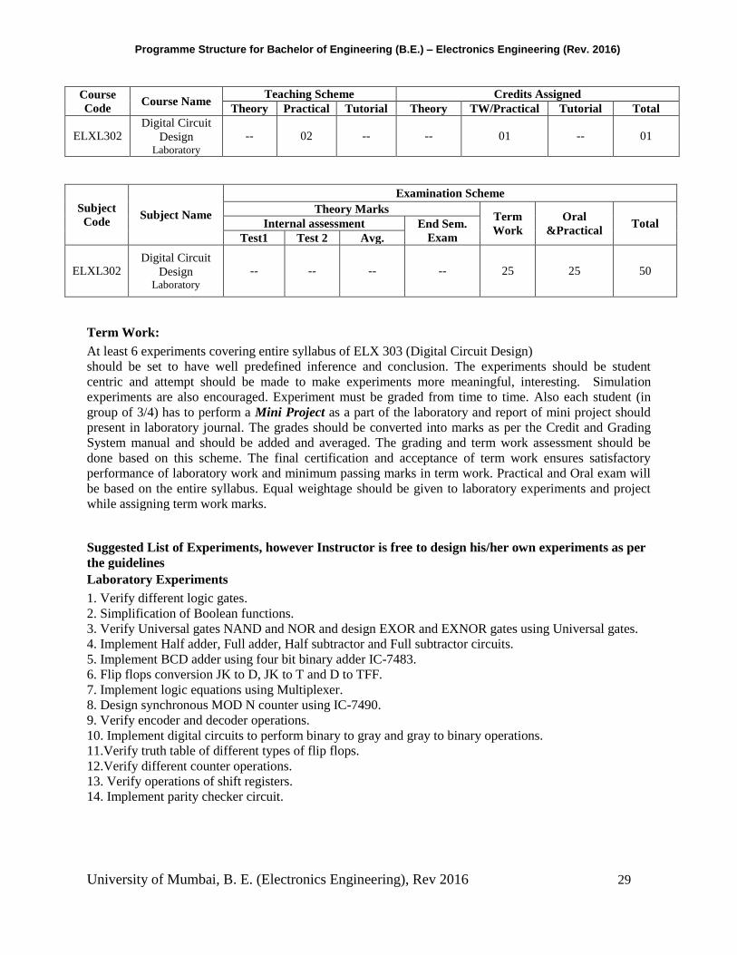
At least 6 experiments covering entire syllabus of ELX 303 (Digital Circuit Design)
should be set to have well predefined inference and conclusion. The experiments should be student
centric and attempt should be made to make experiments more meaningful, interesting. Simulation
experiments are also encouraged. Experiment must be graded from time to time. Also each student (in
group of 3/4) has to perform a Mini Project as a part of the laboratory and report of mini project should
present in laboratory journal. The grades should be converted into marks as per the Credit and Grading
System manual and should be added and averaged. The grading and term work assessment should be
done based on this scheme. The final certification and acceptance of term work ensures satisfactory
performance of laboratory work and minimum passing marks in term work. Practical and Oral exam will
be based on the entire syllabus. Equal weightage should be given to laboratory experiments and project
while assigning term work marks.
1. Verify different logic gates.
2. Simplification of Boolean functions.
3. Verify Universal gates NAND and NOR and design EXOR and EXNOR gates using Universal gates.
4. Implement Half adder, Full adder, Half subtractor and Full subtractor circuits.
5. Implement BCD adder using four bit binary adder IC-7483.
6. Flip flops conversion JK to D, JK to T and D to TFF.
7. Implement logic equations using Multiplexer.
8. Design synchronous MOD N counter using IC-7490.
9. Verify encoder and decoder operations.
10. Implement digital circuits to perform binary to gray and gray to binary operations.
11.Verify truth table of different types of flip flops.
12.Verify different counter operations.
13. Verify operations of shift registers.
14. Implement parity checker circuit.
Suggested List of Experiments, however Instructor is free to design his/her own experiments as per
the guidelines
Laboratory Experiments

Programme Structure for Bachelor of Engineering (B.E.) – Electronics Engineering (Rev. 2016)
University of Mumbai, B. E. (Electronics Engineering), Rev 2016 30
Course
Code
Course Name
Teaching Scheme Credits Assigned
Theory Practical Tutorial Theory TW/Practical Tutorial Total
ELXL303
Electrical
Networks and
Measurements
Laboratory
-- 02 -- -- 01 -- 01
Term Work:
At least 5 experiments covering entire syllabus of ELX 305 (Electronic Instruments and Measurements)
should be set to have well predefined inference and conclusion and minimum of five tutorials covering
entire syllabus of ELX304 (Electrical Network Analysis and Synthesis) with each tutorial shall have a
minimum of four numerical problems solved and duly assessed. Simulation based tutorials shall be based
using any circuit simulation tool like Spice/LTspice are encouraged. The final certification and
acceptance of term work ensures satisfactory performance of laboratory work and minimum passing
marks in term work.
Suggested List of Experiments for ELX305
1.To experimentally determine static characteristics of instruments & perform error analysis
2.To measure low & medium resistances using Kelvin’s Bridge & Kelvin’s Double Bridge
3.To measure high resistances using mega-ohm-meter (megger)
4.Study of CRO & understand various front panel controls
5.Study of function / signal generator & understand various front panel controls
6.Study of spectrum / wave analyser & understand various front panel controls
7.Study of linear variable differential transducer (LVDT)
8.Study of strain gauges
9.Study of thermistor characteristics
10.Study of RTD characteristics
Suggested topics (but not limited to) for tutorial for ELX304 are as follows:
1. Find Open circuit parameters, Short circuit parameters, Hybrid parameters of 2 port network.
2. Obtain the Frequency response of Low pass and High pass filters.
3. Find the time response of R-L and R-C circuits and obtain the time constants.
4. Study of dependent sources – Voltage controlled voltage source and Current controlled current source.
5. Verification of Superposition theorem and Thevenin’s theorem in AC circuits.
6. Time response of a 2nd order system.
Course
Code Course Name
Examination Scheme
Theory Marks Term
Work
Oral
&Practical Total Internal assessment End Sem.
Exam Test1 Test 2 Avg.
ELXL303
Electrical
Network and
Measurement Laboratory
-- -- -- -- 25 -- 25

Programme Structure for Bachelor of Engineering (B.E.) – Electronics Engineering (Rev. 2016)
University of Mumbai, B. E. (Electronics Engineering), Rev 2016 31
7. Calculation of driving point functions for various circuit topologies.
8. Simulation of initial/final conditions (switching) of RLC circuit with DC source on any circuit simulation
platform.
9. Simulation of initial/final conditions (switching) of RLC circuit with AC source on any circuit simulation
platform.
Programme Structure for Bachelor of Engineering (B.E.) – Electronics Engineering (Rev. 2016)
University of Mumbai, B. E. (Electronics Engineering), Rev 2016 32
Course
Code
Course Name
Teaching Scheme Credits Assigned
Theory Practical Tutorial Theor
y TW/Practical Tutorial Total
ELXL304
Object Oriented
Programming
Methodology Laboratory
02
Classwise
02
Batchwise -- -- 02 -- 02
Course
Code Course Name
Examination Scheme
Theory Marks Term
Work
Oral
&Practical Total Internal assessment End Sem.
Exam Test1 Test 2 Avg.
ELXL304
Object Oriented
Programming
Methodology Laboratory
-- -- -- -- 25 25 50
Prerequisite:
FEC205: Structured Programming Approach
Course Objective:
1.To learn the object oriented programming concepts.
2.To study various java programming concept like multithreading, exception handling, packages etc.
3.To explain components of GUI based programming.
Course Outcomes: At the end of the course Student should be able:
1.To apply fundamental programming constructs.
2.To illustrate the concept of packages, classes and objects.
3.To elaborate the concept of strings, arrays and vectors.
4.To implement the concept of inheritance and interfaces.
5.To implement the notion of exception handling and multithreading.
6.To develop GUI based application.

Programme Structure for Bachelor of Engineering (B.E.) – Electronics Engineering (Rev. 2016)
University of Mumbai, B. E. (Electronics Engineering), Rev 2016 33
Module
No
Unit
No
Topic Hours
1
Introduction to Object Oriented Programming
02
1.1 OOP Concepts: Object, Class, Encapsulation, Abstraction, Inheritance,
Polymorphism
1.2 Features of Java, JVM
1.3 3 Basic Constructs/Notions: Constants, variables and data types, Operators and
Expressions, Revision of Branching and looping
2
Classes, Object and Packages
05
2.1 Class, Object, Method
2.2 Constructor, Static members and methods
2.3 Passing and returning Objects
2.4 Method Overloading
2.5 Packages in java, creating user defined packages, access specifiers.
3
Array, String and Vector
04 3.1 Arrays, Strings, String Buffer
3.2 Wrapper classes, Vector
4
Inheritance and Interface
03 4.1 Types of Inheritance, super keyword, Method Overriding, abstract class and
abstract method, final keyword
4.2 Implementing interfaces, extending interfaces
5
Exception Handling and Multithreading
04 5.1 Error vs Exception, try, catch, finally, throw, throws, creating own exception
5.2 Thread lifecycle, Thread class methods, creating threads, Synchronization
6
GUI programming in JAVA
6.1 Applet: Applet life cycle, Creating applets, Graphics class methods, Font and
Color class, parameter passing.
6.2 Event Handling: Event classes and event listener

Programme Structure for Bachelor of Engineering (B.E.) – Electronics Engineering (Rev. 2016)
University of Mumbai, B. E. (Electronics Engineering), Rev 2016 34
6.3 Introduction to AWT: Working with windows, Using AWT controls- push
Buttons, Label, Text Fields, Text Area, Check Box, and Radio Buttons. 08
6.4 Programming using JDBC: Introduction to JDBC, JDBC Drivers &
Architecture.
Total 26
Text books:
1. Herbert Schildt, ‘JAVA: The Complete Reference’, Ninth Edition, Oracle Press.
2. Sachin Malhotra and Saurabh Chaudhary, “Programming in Java”, Oxford University Press, 2010
Reference Books:
1. Ivor Horton, ‘Beginning JAVA’, Wiley India.
2. DietalandDietal, ‘Java: How to Program’, 8/e,PHI
3. ‘JAVA Programming’, Black Book, Dreamtech Press.
4. ‘Learn to Master Java programming’, Staredusolutions
Digital Material:
1. www.nptelvideos.in
2. www.w3schools.com
3. http://spoken-tutorial.org
4. www.staredusolutions.org
Suggested List of Programming Assignments/Laboratory Work:
1.Program on various ways to accept data through keyboard and unsigned right shift operator.
2.Program on branching, looping, labelled break and labelled continue.
3.Program to create class with members and methods, accept and display details for single object.
4.Program on constructor and constructor overloading
5.Program on method overloading
6.Program on passing object as argument and returning object
7.Program on creating user defined package
8.Program on 1D array
9.Program on 2D array
10.Program on String
11.Program on StringBuffer
12.Program on Vector
13.Program on single and multilevel inheritance (Use super keyword)
14.Program on abstract class
15.Program on interface demonstrating concept of multiple inheritance
16.Program on dynamic method dispatch using base class and interface reference.
17.Program to demonstrate try, catch, throw, throws and finally.
18.Program to demonstrate user defined exception
19.Program on multithreading
20.Program on concept of synchronization
21.Program on Applet to demonstrate Graphics, Font and Color class.

Programme Structure for Bachelor of Engineering (B.E.) – Electronics Engineering (Rev. 2016)
University of Mumbai, B. E. (Electronics Engineering), Rev 2016 35
22.Program on passing parameters to applets
23.Program to create GUI application without event handling using AWT controls
24.Program to create GUI application with event handling using AWT controls
25.Mini Project based on content of the syllabus. (Group of 2-3 students)
Term Work:
At least 10-12 experiments covering entire syllabus of ELXL304 (Object Oriented Programming
Methodology) should be set to have well predefined inference and conclusion. The experiments should be
student centric and attempt should be made to make experiments more meaningful, interesting. Experiment
must be graded from time to time. Also each student (in group of 3/4) has to perform a Mini Project as a
part of the laboratory and report of mini project should present in laboratory journal. The grades should be
converted into marks as per the Credit and Grading System manual and should be added and averaged. The
grading and term work assessment should be done based on this scheme. The final certification and
acceptance of term work ensures satisfactory performance of laboratory work and minimum passing marks in
term work. Practical and Oral exam will be based on the entire syllabus. Equal weightage should be given to
laboratory experiments and project while assigning term work marks.

Programme Structure for Bachelor of Engineering (B.E.) – Electronics Engineering (Rev. 2016)
University of Mumbai, B. E. (Electronics Engineering), Rev 2016 36
S.E. (Electronics Engineering) – Semester IV
@1 hour tutorial classwise
Course
Code Course Name
Examination Scheme – Semester IV
Theory
Term
Work
Oral
/Prac
Total Internal Assessment
(IA)
End
Sem
Exam
Marks
Exam
Duration
(Hours) Test
I
Test
II
AVG.
ELX401 Applied Mathematics IV 20 20 20 80 3 25 --- 125
ELX 402 Electronic Devices and Circuits II 20 20 20 80 3 --- --- 100
ELX 403 Microprocessors and Applications 20 20 20 80 3 --- --- 100
ELX 404 Digital System Design 20 20 20 80 3 --- --- 100
ELX 405 Principles of Communication
Engineering 20 20 20 80 3 --- --- 100
ELX 406 Linear Control Systems 20 20 20 80 3 --- --- 100
ELXL401 Electronic Devices and Circuits II
Laboratory 25 25 50
ELXL402 Microprocessors and Applications
Laboratory 25 25 50
ELXL 403 Digital System Design Laboratory 25 25 50
ELXL404 Principles of Communication
Engineering Laboratory 25 -- 50
Total 120 120 120 480 18 100 75 800
Course
Code Course Name
Teaching Scheme
(Contact Hours) Credits Assigned
Theory Practical Tutorial Theory Practical Tutorial Total
ELX401 Applied Mathematics IV 04 --- 01@ 04 --- 01 05
ELX 402 Electronic Devices and Circuits
II 04 --- --- 04 --- --- 04
ELX 403 Microprocessors and Applications 04 --- --- 04 --- --- 04
ELX 404 Digital System Design 04 --- --- 04 --- --- 04
ELX 405 Principles of Communication
Engineering 04 --- --- 04 --- --- 04
ELX 406 Linear Control Systems 04 --- --- 04 --- --- 04
ELXL 401 Electronic Devices and Circuits
II Lab. 02 --- --- 01 --- 01
ELXL 402 Microprocessors and Applications
Lab. 02 --- --- 01 --- 01
ELXL 403 Digital System Design Lab. 02 --- --- 01 --- 01
ELXL 404 Principles of Communication
Engineering Lab. 02 --- --- 01 --- 01
Total 24 08 01 24 04 01 29

Programme Structure for Bachelor of Engineering (B.E.) – Electronics Engineering (Rev. 2016)
University of Mumbai, B. E. (Electronics Engineering), Rev 2016 37
Course
Code
Course
Name
Teaching Scheme Credits Assigned
Theory Practical Tutorial Theory TW/
Practical Tutorial Total
ELX401
Applied
Mathematics
IV
04 -- 01 04 -- 01 05
Course
Code Course Name
Examination Scheme
Theory Marks Term
Work
Oral
&Practical Total Internal assessment End Sem.
Exam Test1 Test 2 Avg.
ELX401
Applied
Mathematics
IV 20 20 20 80 25 -- 100
Prerequisite:
FEC 101: Applied Mathematics I
FEC 201: Applied Mathematics II
ELX 301: Applied Mathematics III
Course objectives:
1. To build the strong foundation in Mathematics of students needed for the field of
Electronics and Telecommunication Engineering
2. To provide students with mathematics fundamentals necessary to formulate, solve and analyses
complex engineering problems.
3. To prepare student to apply reasoning informed by the contextual knowledge to engineering practice.
4. To prepare students to work as part of teams on multi-disciplinary projects.
Course outcomes: 1 Students will demonstrate basic knowledge of Calculus of variation, Vector Spaces, Matrix Theory,
Random Variables, Probability Distributions, Correlation and Complex Integration.
2 Students will demonstrate an ability to identify and Model the problems in the field of Electronics
and Telecommunication and solve it.
3 Students will be able to apply the application of Mathematics in Telecommunication Engineering.

Programme Structure for Bachelor of Engineering (B.E.) – Electronics Engineering (Rev. 2016)
University of Mumbai, B. E. (Electronics Engineering), Rev 2016 38
Module
No.
Unit
No.
Topics Hrs.
1 Calculus of Variation: 06
2
1.1 Euler’s Langrange equation, solution of Euler’s Langrange equation
(only results for different cases for Function) independent of a variable,
independent of another variable, independent of differentiation of a
variable and independent of both variables
1.2 Isoperimetric problems, several dependent variables
1.3 Functions involving higher order derivatives: Rayleigh-Ritz method
Linear Algebra: Vector Spaces 06
2.1 Vectors in n-dimensional vector space: properties, dot product, cross
product, norm and distance properties in n-dimensional vector space.
2.2 Vector spaces over real field, properties of vector spaces over real field,
subspaces.
2.3 The Cauchy-Schwarz inequality, Orthogonal Subspaces, Gram-Schmidt
process.
3 Linear Algebra: Matrix Theory 10
3.1 Characteristic equation, Eigen values and Eigen vectors, properties of
Eigen values and Eigen vectors
3.2 Cayley-Hamilton theorem (without proof), examples based on
verification of Cayley- Hamilton theorem.
3.3 Similarity of matrices, Diagonalisation of matrices.
3.4
Functions of square matrix, derogatory and non-derogatory matrices.
4 Probability 10
4.1 Baye’s Theorem (without proof)
4.2 Random variable: Probability distribution for discrete and continuous
random variables, Density function and distribution function,
expectation, variance.
4.3 Moments, Moment Generating Function.
4.4 Probability distribution: Binomial distribution, Poisson & normal
distribution (For detailed study)
5 Correlation 04
5.1 Karl Pearson’s coefficient of correlation,Covariance,Spearman’s Rank
correlation,
5.2 Lines of Regression.
6 Complex integration 12
6.1 Complex Integration:Line Integral, Cauchy’s Integral theorem for
simply connected regions, Cauchy’s Integral formula.
6.2 Taylor’s and Laurent’s Series
6.3 Zeros, singularities, poles of f(z), residues, Cauchy’s Residue theorem.
6.4 Applications of Residue theorem to evaluate real Integrals of different
types.
Total 48

Programme Structure for Bachelor of Engineering (B.E.) – Electronics Engineering (Rev. 2016)
University of Mumbai, B. E. (Electronics Engineering), Rev 2016 39
Text books: 1. H.K. Das, “Advanced engineering mathematics”, S . Chand, 2008
2. A. Datta, “Mathematical Methods in Science and Engineering”, 2012
3. B.S. Grewal, “Higher Engineering Mathematics”, Khanna Publication
4. P.N.Wartilar&J.N.Wartikar, “A Text Book of Applied Mathematics” Vol.I and
II,VidyarthiGrihaPrakashan., Pune.
Reference Books:
1. B. V. Ramana, “Higher Engineering Mathematics”, Tata Mc-Graw Hill Publication
2. Wylie and Barret, “Advanced Engineering Mathematics”, Tata Mc-Graw Hill 6th Edition
3. Erwin Kreysizg, “Advanced Engineering Mathematics”, John Wiley & Sons, Inc
4. Seymour Lipschutz ,“Beginning Linear Algebra” Schaum’s outline series, Mc-Graw Hill
Publication
5.Seymour Lipschutz, “Probability” Schaum’s outline series, Mc-Graw Hill Publication
Internal Assessment (IA):
Two tests must be conducted which should cover at least 80% of syllabus. The average marks of both the
tests will be considered as final IA marks.
End Semester Examination:
1. Question paper will comprise of 6 questions, each carrying 20 marks.
2. The students need to solve total 4 questions.
3. Question No. 1 will be compulsory and based on entire syllabus.
4. Remaining questions (Q2 to Q6) will be set from all modules.
5. Weightage of each module in question paper will be proportional to the number of respective lecture hours
mentioned in the syllabus.
Term Work/ Tutorial: At least 08 assignments covering entire syllabus must be given during the “class wise tutorial’. The assignments should be students centric and an attempt should be made to make assignments more meaningful, interesting and innovative. Term work assessment must be based on the overall performance of the student with every assignment graded from time to time. The grades will be converted to marks as per “credit and grading system” manual and should be added and averaged. Based on above scheme grading and term work assessment should be done.

Programme Structure for Bachelor of Engineering (B.E.) – Electronics Engineering (Rev. 2016)
University of Mumbai, B. E. (Electronics Engineering), Rev 2016 40
Course
Code
Course
Name
Teaching Scheme Credits Assigned
Theory Practical Tutorial Theory TW/
Practical Tutorial Total
ELX402
Electronic
Devices
&Circuits-II
04 -- -- 04 -- -- 04
Prerequisite:
FEC105: Basic Electrical & Electronics Engineering
ELX302: Electronic Device and Circuits I
Course Objectives:
1. To enhance comprehension capabilities of students through understanding of electronic devices and circuits
2. To perform DC and AC analysis of single stage and multistage amplifiers
3. To introduce and motivate students to the use of advanced microelectronic devices
4. To design electronic circuits using semiconductor devices.
Course Outcome:
1. Students will be able to Ability to understand amplifiers through frequency response.
2. Students will be able to perform DC and Ac analysis of single stage and multistage amplifiers, oscillators,
differential amplifiers and power amplifiers.
3. Students will be able to derive expression for performance parameters in terms of circuit and device parameters.
4. Student will be able to select appropriate circuit for given specifications/applications.
5. Students will be able to explain working and construction details of special, semiconductor devices.
Course
Code
Course
Name
Examination Scheme
Theory Marks Term
Work
Oral
&Practical Total Internal assessment End Sem.
Exam Test1 Test 2 Avg.
ELX402
Electronic
Devices &
Circuits-II 20 20 20 80 -- -- 100

Programme Structure for Bachelor of Engineering (B.E.) – Electronics Engineering (Rev. 2016)
University of Mumbai, B. E. (Electronics Engineering), Rev 2016 41
Module
No.
Topics Hours
1 Frequency response of amplifiers.
8 1.1 High frequency equivalent circuit of BJT and MOSFET, Miller's theorem, effect of Miller's
capacitance, unity gain bandwidth
1.2 Effect of coupling, bypass and load capacitors on single stage BJT and MOSFET amplifiers.
2 Frequency Response of Multistage Amplifiers.
6 2.1 Effect of parasitic capacitances on BJT and MOSFET amplifiers.
Low, mid and high frequency response of multistage amplifiers (CE-CE, CE-CB, CS-CS,
CS-CG)
3 Feedback Amplifiers and Oscillators
8
3.1 Types of Negative Feedback block diagram representation, Effect of negative feedback on
Input impedance, Output impedance, Gain and Bandwidth with derivation, feedback
topologies (Introduction only).
3.2 Positive feedback and principle of oscillations, RC oscillators: Phase shift oscillators, Wien
bridge oscillators, LC Oscillators: Hartley, Colpitts and clapp, Tunned Oscillator, Twin T
Oscillator, Crystal Oscillator (BJT circuit analysis).
4 Differential Amplifiers
10
4.1 MOSFET current sources, Cascode current mirror, advanced MOSFET active load, small
signal analysis: MOSFET active load
4.2 Basic MOSFET differential amplifier, DC characteristics, transfer characteristics,
differential and common mode input impedances.
4.3 MOSFET differential amplifier with active load, MOSFET differential amplifier with
cascode active load,
5 Power Amplifiers
8 Power BJTs, Heat sinks, Power BJTs, Power MOSFETs, Heat Sinks, Class A, Class B,
Class C and Class AB
operation, Power efficiency, Class AB output stage with diode biasing, VBE multiplier
biasing, input buffer transistors, Darlington configuration.
6 Special Semiconductor Devices - II 8
PNPN diode, SCR, DIAC, TRIAC, UJT, IGBT, HEMT, Gunn diode, IMPATT diode, HBT
Total Hours 48

Programme Structure for Bachelor of Engineering (B.E.) – Electronics Engineering (Rev. 2016)
University of Mumbai, B. E. (Electronics Engineering), Rev 2016 42
Text Books: 1. Millman and Halkies, “Integrated Electronics”, TATA McGraw Hill.
2. Donald A. Neamen, “Electronic Circuit Analysis and Design”, TATA McGraw Hill, 2nd Edition
Reference Books: 1. Boylestad," Electronic Devices and Circuit Theory", Pearson
2. David A. Bell, “Electronic Devices and Circuits”, Oxford, Fifth Edition.
3. Muhammad H. Rashid, “Microelectronics Circuits Analysis and Design”, Cengage
4. S. Salivahanan, N. Suresh Kumar,“Electronic Devices and Circuits”, Tata McGraw Hill,
5. Adel S. Sedra, Kenneth C. Smith and Arun N Chandorkar,” Microelectronic Circuits Theory and
Applications”, International Version, OXFORD International Students Edition, Fifth Edition.
Internal Assessment (IA):
Two tests must be conducted which should cover at least 80% of syllabus. The average marks of both the
tests will be considered as final IA marks.
End Semester Examination:
1. Question paper will comprise of 6 questions, each carrying 20 marks.
2. The students need to solve total 4 questions.
3. Question No. 1 will be compulsory and based on entire syllabus.
4. Remaining questions (Q2 to Q6) will be set from all modules.
5. Weightage of each module in question paper will be proportional to the number of respective lecture hours
mentioned in the syllabus.

Programme Structure for Bachelor of Engineering (B.E.) – Electronics Engineering (Rev. 2016)
University of Mumbai, B. E. (Electronics Engineering), Rev 2016 43
Course
Code Course Name
Teaching Scheme Credits Assigned
Theory Practic
al Tutorial Theory
TW/
Practical Tutorial Total
ELX403 Microprocessors &
Applications 04 -- -- 04 -- -- 04
Prerequisite:
ELX303:Digital Circuit Design
Course Objectives:
1. To develop background knowledge and core expertise in microprocessor.
2. To study the concepts and basic architecture of 8086 and Co-processor 8087.
3. To know the importance of different peripheral devices and their interfacing to 8086.
4. To know the design aspects of basic microprocessor.
5. To write assembly language programs in microprocessor for various applications.
Course Outcomes:
1.Students will be able to understand and explain 16-bit microprocessor architecture.
2.Students will be able to understand and write programmes for 8086 microprocessor.
3.Students will be able to use various peripheral devices to design Single Board
Computer(SBC). 4.Students will be able to understand and explain 32-bit microprocessor architecture.
Course
Code
Course
Name
Examination Scheme
Theory Marks Term
Work
Oral
&Practical Total Internal assessment End Sem.
Exam Test1 Test 2 Avg.
ELX403
Microprocessors
and Applications 20 20 20 80 -- -- 100

Programme Structure for Bachelor of Engineering (B.E.) – Electronics Engineering (Rev. 2016)
University of Mumbai, B. E. (Electronics Engineering), Rev 2016 44
Module
No.
Topics Hrs.
1. Intel 8086 Architecture: Major features of 8086 processor, 8086 CPU
Architecture and the pipelined operation, Programmer’s Model, Memory
Segmentation and 8086 pin description in detail.
05
2. Instruction Set of 8086 and Programming: Addressing modes of
8086, Instruction Set of 8086 microprocessor in detail, Assembler
directives,Procedures and Macros, Programming 8086 in assembly
language, Mixed mode Programming with C-language and assembly
language.
07
3. 8086 Interrupts: Interrupt types in 8086, Dedicated interrupts, Software
interrupts, Programming examples related to INT 21H (DOS Interrupts).
05
4. Designing the 8086 CPU module: Generating the 8086 System Clock
and Reset Signals using 8284 clock generator, 8086 Minimum and
Maximum Mode CPU Modules, Minimum and Maximum Mode Timing
Diagrams, Memory interfacing.
07
5. Single Board Computer Design: 8086 – 8087 coprocessor interfacing. Functional Block Diagram and
description, Operating Modes, Control Word Formats and Applications
of the Peripheral Controllers - 8255-PPI,8259- PIC and 8237-DMAC.
Keyboard and Seven Segment Display Interface using 8255. System
design using peripheral controllers.
12
6. Introduction to 32-bit Intel Pentium Architecture: Features of
Pentium Processor, Pentium Superscalar architecture, Pipelining, Branch
Prediction, Instruction and Data cache.
12
Total 48

Programme Structure for Bachelor of Engineering (B.E.) – Electronics Engineering (Rev. 2016)
University of Mumbai, B. E. (Electronics Engineering), Rev 2016 45
Text Books:
1)8086/8088 family: Design Programming and Interfacing: By John Uffenbeck (Pearson Education)
2)Microprocessor and Interfacing: By Douglas Hall (TMH Publication)
3)The Intel Microprocessor family: Hardware and Software principles and Applications: By James
L. Antonakos (Cengage Learning)
Reference Books:
1) 8086 Microprocessor Programming and Interfacing the PC: By Kenneth Ayala (West
Publication)
2) Pentium Processor System Architecture: By Don Anderson & Tom Shanley (Mindshare, Inc.)
(Addison-Wesley Publisher)
3) The INTEL Microprocessors, Architecture, Programming and Interfacing: By Barry B. Brey
(PearsonPublishers, 8th
Edition)
4) Microcomputer Systems: 8086/8088 family Architecture, Programming and Design: By Liu &
Gibson (PHI Publication).
Internal Assessment (IA):
Two tests must be conducted which should cover at least 80% of syllabus. The average marks of
both the test will be considered as final IA marks
End Semester Examination:
1. Question paper will comprise of 6 questions, each carrying 20 marks.
2. The students need to solve total 4 questions.
3. Question No. 1 will be compulsory and based on entire syllabus.
4. Remaining questions (Q2 to Q6) will be set from all modules.
5. Weightage of each module in question paper will be proportional to the number of respective lecture hours
mentioned in the syllabus.

Programme Structure for Bachelor of Engineering (B.E.) – Electronics Engineering (Rev. 2016)
University of Mumbai, B. E. (Electronics Engineering), Rev 2016 46
Course
Code Course Name
Teaching Scheme Credits Assigned
Theory Practic
al
Tutoria
l Theory
TW/Practica
l Tutorial Total
ELX404 Digital System
Design 04 -- -- 04 -- -- 04
Prerequisite:
ELX303: Digital Circuit Design
Course Objectives:
1. To perform analysis of synchronous sequential circuits.
2. To perform the design of synchronous and asynchronous counters using intuitive approaches.
3. To apply fundamental design procedure for synchronous sequential circuits; consisting of the
steps as construction of initial state transition table/diagram, perform state reduction and state
assignment, develop flip-flop excitations, and design of registers and counters.
4. To understand the basics of Hardware Description language. .
5. To make VHDL implementations on the structured design of synchronous sequential circuits.
6. To apply algorithmic state machines (ASMs) approach for large-size digital system design;
consisting of the steps as development of ASM charts and ASM blocks, make state assignment
on ASMs, and perform data path and control path designs.
Course Outcome:
1. Students will be able to design and implement synchronous sequential logic circuits.
2. Students will be able to analyze various types of digital logic circuits.
3. Students will be able to understand engineering concepts in the design of digital circuits.
4. Students will be able to understand the role of hardware description languages in digital circuit
implementation.
5. Students will be able to describe simple hardware functions using a hardware description
language.
6. Students will be able to understand the purpose of and steps involved in digital circuit
implementation using Field-Programmable Gate Arrays.
Course
Code
Course
Name
Examination Scheme
Theory Marks Term
Work
Oral
&Practical Total Internal assessment End Sem.
Exam Test1 Test 2 Avg.
ELX404
Digital System
Design 20 20 20 80 -- -- 100

Programme Structure for Bachelor of Engineering (B.E.) – Electronics Engineering (Rev. 2016)
University of Mumbai, B. E. (Electronics Engineering), Rev 2016 47
Module
No.
Topics Hrs.
1
Sequential logic design
09
Mealy and Moore models, state machine notations, clocked synchronous state
machine analysis, construction of state diagram, sequence detector (word
problem), state reduction techniques (inspection, partition and implication
chart method), clocked synchronous state machine design, design examples
like a few simple machines and traffic light controller, vending machine.
2
Algorithmic State Machine (ASM) Chart and Register Transfer
Luanguage(RTL)
08
Standard symbols for ASM Chart, Realization techniques for sequential/logic
functions using ASM Chart, Top Down Design Example, Generalized ASM
output, ASM Chart representation of control unit, RTL, Construction of data
unit using RTL Description, Timing of connection and transfer, sequencing of
control, Combinational logic and conditional transfer, Graphical and RTL Bus
notation, Design examples of waveform controllable generator ,pulse width
adjustor using ASM chart, design data unit and control unit for sequential
circuits using RTL Description.
3
Sequential logic design practices
09
Synchronous counter design and applications, MSI asynchronous counters (IC
7490, 7493), MSI synchronous counters (IC 74161, 74163, 74168, 74169)
and applications, decoding binary counter states, MSI shift registers,
Synchronous design methodology, impediments in synchronous design,
synchronizer failure and metastability.
4
Introduction to VHDL
08
Introduction to Hardware Description Language, Core features of VHDL, data types, concurrent and sequential statements, data flow, behavioral, structural architectures, subprograms, Examples like Adder, subtractor, Multiplexers, De-multiplexers, encoder, decoder.
5
Design of Sequential circuits using VHDL
08 VHDL code for flip flop, counters, registers, Moore, Mealy type FSMs, Serial
adders, sequence detector.
6
Programmable Logic Devices
06 ROM, RAM, SRAM, PLA, PAL, CPLD and FPGA architecture. Numerical
based on PLA and PAL.
Total 48

Programme Structure for Bachelor of Engineering (B.E.) – Electronics Engineering (Rev. 2016)
University of Mumbai, B. E. (Electronics Engineering), Rev 2016 48
Text Books:
1. Digital Logic Applications and Design – John M. Yarbrough, Thomson Publications, 2006
2. Digital Design, Morris Mano Second Edition, PHI, 2002
3. Volnei A. Pedroni, “Circuit Design with VHDL” MIT Press (2004)
Reference Books:
1. Digital Design Principles and Practices, 3rd ed. by Wakerly. Prentice Hall, 2000
2. Digital Design – Morris Mano, M.D.Ciletti, 4th Edition, PHI
3. Digital Circuits and Logic Design – Samuel C. Lee , PHI
4. William I.Flectcher, “An Engineering Approach to Digital Design”, PrenticeHall of India.
5. Parag K Lala, “Digital System design using PLD”, BS Publications, 2003.
6. Charles H. Roth Jr., “Fundamentals of Logic design”, Thomson Learning, 2004.
7. Stephen Brown, Zvonko Vranesic, “Fundamentals of Digital Logic Design” McGraw Hill, 2nd
edition Charles H.Roth Jr “Fundamentals of Logic Design” Thomson Learning 2004
Internal Assessment (IA): Two tests must be conducted which should cover at least 80% of syllabus. The average marks of
both the test will be considered as final IA marks.
End Semester Examination:
1. Question paper will comprise of 6 questions, each carrying 20 marks.
2. The students need to solve total 4 questions.
3. Question No. 1 will be compulsory and based on entire syllabus.
4. Remaining questions (Q2 to Q6) will be set from all modules.
5. Weightage of each module in question paper will be proportional to the number of respective lecture hours
mentioned in the syllabus.

Programme Structure for Bachelor of Engineering (B.E.) – Electronics Engineering (Rev. 2016)
University of Mumbai, B. E. (Electronics Engineering), Rev 2016 49
Course
Code Course Name
Teaching Scheme Credits Assigned
Theory Practic
al
Tutoria
l Theory TW/Practical Tutorial Total
ELX405
Principles of
Communication
Engineering
04 -- -- 04 -- -- 04
Prerequisite:
Applied Mathematics-III
Applied Mathematics-IV
Course Objectives:
1. Understand the need for various analog modulation techniques
2. Analyse the characteristics of the receivers
3. Understand pulse modulation methods
4. Identify the necessity of multiplexing
Course Outcomes: 1. Students will be able to comprehend the need for various components in analog communication
systems
2. Students will be able to analyse various analog modulation methods
3. Students will be able to design modulators, demodulators for amplitude and frequency modulated
systems.
4. Students will be able to assess the characteristics of pulse modulation techniques.
5. Recognize the need for multiplexing techniques.
Course
Code
Course
Name
Examination Scheme
Theory Marks Term
Work
Oral
&Practical Total Internal assessment End Sem.
Exam Test1 Test 2 Avg.
ELX405
Principles of
Communication
Engineering 20 20 20 80 -- -- 100

Programme Structure for Bachelor of Engineering (B.E.) – Electronics Engineering (Rev. 2016)
University of Mumbai, B. E. (Electronics Engineering), Rev 2016 50
Module
No.
Unit
No.
Topics Hrs
1
Introduction to Electronic Communication
06
1.1 Introduction: Electromagnetic frequency spectrum, concepts of wave
propagation-ground wave, sky wave and space wave
1.2 Elements of communication systems: Information sources,
communication channels, noise, sources of noises, need for modulation,
bandwidth and power trade-off.
1.3 1.3 Representation of the signals: Fourier series, Fourier transform, two
sided spectrum
2
Amplitude Modulation and demodulation
10
2.1 Amplitude Modulation : Types of Analog Modulation, Principles of
Amplitude Modulation , AM for a Complex Modulating Signal, AM
Power Distribution, AM Current Distribution, Limitations of AM , AM
modulators and Demodulator
2.2 Types of AM: Modulation & Demodulation Techniques: DSB-SC, SSB-SC ,
Vestigial-Sideband (VSB) Modulation , Comparison of AM, DSBSC, SSB
and VSB
2.3 2.3 Applications of AM
3
Angle modulation and demodulation
08 3.1 Frequency Modulation: Principles of Angle Modulation, Theory of FM—
Basic Concepts, Spectrum Analysis of FM Wave, Narrowband and
Wideband FM, Noise triangle,Pre-emphasis, de-emphasis FM Generation:
Direct methods and Indirect method,FM Detection: Frequency discriminator
and Phase discriminator methods
3.2 Phase Modulation : Theory of Phase Modulation, Relationship between FM
and PM, Advantages and Disadvantages of Angle Modulation, Comparison
of AM, FM and PM
3.3 3 Applications of FM and PM
4
Radio Transmitters and Receivers
08
4.1 Radio receivers: Receiver Characteristics : Sensitivity, Selectivity, Fidelity,
Image frequency rejection ratio, TRF Receivers and its characteristics ,
Concept of Heterodyning , Superheterodyne Receiver , choice of
Intermediate frequency
4.2 AM Transmitters and Receivers: AM Radio Transmitters, AM Radio
Receivers, Practical diode detector, Automatic Gain control(AGC), Types of
AGC.
4.3 FM Transmitters and Receivers: FM Transmitters, FM Receivers ,
Automatic Frequency control(AFC) , Importance of Limiter,Communication
Receivers
5
Pulse-Modulation and demodulation
08 5.1 Introduction to digital transmission of signals: comparison of Digital
Analog Transmissions, Concept of regenerative Repeater
5.2 Sampling and quantization: Sampling Theorem, Aliasing error, Natural
Sampling , Flat top sampling, Quantization of Signals
5.3 Pulse Modulation Techniques :Generation and detection of Pulse

Programme Structure for Bachelor of Engineering (B.E.) – Electronics Engineering (Rev. 2016)
University of Mumbai, B. E. (Electronics Engineering), Rev 2016 51
Amplitude Modulation (PAM), Pulse Width Modulation (PWM), Pulse
Position Modulation (PPM)
6
PCM and Multiplexing
08
6.1 PCM: Pulse-Code Modulation (PCM), Noise Performance of PCM Systems,
Differential PCM (DPCM), Adaptive Differential PCM (ADPCM), Delta
Modulation, Adaptive Delta Modulation, Continuous Variable Slope DM
(CVSDM), Comparison of PCM Techniques
6.2 Multiplexing in Telecommunications Networks, Synchronous and
Asynchronous TDM, Single-Channel PCM Transmission System, T1 Digital
Carrier System, FDM
Total 48
Text Books:
1.Kennedy and Davis “Electronics communication system ”,Tata McGraw Hill
2.T L Singal , Analog and Digital communication, Tata McGraw Hill
3.R P Singh &Sapre , Analog and Digital communication, Tata McGraw Hill 2nd Ed.
Reference books :
1.Wayne Tomasi “Electronics communication systems” Pearson Education, Third Edition, 2001.
2.Taub and Schilling “Principles of communication systems”, Tata McGraw Hill
3.Roy Blake, “Electronics communication system”, Thomson learning, Second Edition.
4.B.P. Lathi “Modern Digital and analog Communication system” Third Edition, OXFORD
5.Robert J. Schoenbeck “Electronics communications modulation and transmission”
6.Lean W couch “Digital and Analog communication system”, Pearson Education, Sixth Edition
7.Roddy Coolen, “Electronic Communications” PHI
Internal Assessment (IA):
Two tests must be conducted which should cover at least 80% of syllabus. The average marks of both thetest
will be considered as final IA marks.
End Semester Examination:
1. Question paper will comprise of 6 questions, each carrying 20 marks.
2. The students need to solve total 4 questions.
3. Question No. 1 will be compulsory and based on entire syllabus.
4. Remaining questions (Q2 to Q6) will be set from all modules.
5. Weightage of each module in question paper will be proportional to the number of respective lecture hours
mentioned in the syllabus.

Programme Structure for Bachelor of Engineering (B.E.) – Electronics Engineering (Rev. 2016)
University of Mumbai, B. E. (Electronics Engineering), Rev 2016 52
Course
Code Course Name
Teaching Scheme Credits Assigned
Theory Practic
al
Tutoria
l Theory TW/Practical Tutorial Total
ELX406 Linear Control
System 04 -- -- 04 -- -- 04
Prerequisites Topics:
Differential Equations; Laplace transforms and Matrices.
Course Objectives:
1. To teach fundamental concepts of Control systems and mathematical modelling of the system.
2. To teach the concepts of time response and frequency response analysis of Control Systems.
3. To teach the concepts of state variable models as applicable to linear time invariant systems
4. To teach concepts of controllers and compensators
Course Outcomes:
1. Students will be able to understand the basic concepts of control system and identify control systems in
real life applications.
2. Students will be able to derive the mathematical model of different types of control systems and represent
them in various forms
3. Students will be able to analyze systems using time domain analysis techniques
4. Students will be able to apply concepts of frequency domain techniques in stability analysis of control
systems
5. Students will be able to create state variable models of systems andanalyze their controllability,
observability and time response
6. Students will be able to identify controllers and compensators in different controllers.
Course
Code
Course
Name
Examination Scheme
Theory Marks Term
Work
Oral
&Practical Total Internal assessment End Sem.
Exam Test1 Test 2 Avg.
ELX406
Linear Control
System 20 20 20 80 -- -- 100

Programme Structure for Bachelor of Engineering (B.E.) – Electronics Engineering (Rev. 2016)
University of Mumbai, B. E. (Electronics Engineering), Rev 2016 53
Module
No.
Topics Hrs.
1
Models for Control System
08
1.1 Introduction: Open loop and closed loop systems; feedback and feed-
forward control structure; examples of control systems.
1.2 Mathematical Modelling: Types of models; Impulse response model;
State Variable model and Transfer function model for Electrical, Mechanical
and Thermal systems
1.3 Manipulations: Block Diagram Representation of complex systems,
Block diagram reduction, Signal flow graph and the Mason’s gain rule for
determining overall transfer function of Single Input, Single output systems
2
Time Response Analysis
08
2.1 Dynamic Response: Standard test signals; Transient and steady state
behaviour of first and second order systems 2.2. Performance Specifications for a second order system and derivations for rise
time, settling time, peak time, peak overshoot and steady state error
2.3. Steady State errors in feedbackcontrol systems and their types, Error
constants and type of system.
3
State Variable Models
10
3.1 State variable models: State variable models of electrical systems
3.2 State transition equation: Concept of state transition matrix; Properties
of state transition matrix; Solution of homogeneous systems; solution of
nonhomogeneous systems.
3.3 Controllability and Observability: Concept of controllability;
Controllability analysis of LTI systems; Concept of observability;
Observability
analysis of LTI systems using Kalman approach.
4
Stability Analysis in Time Domain
06 4.1 Concepts of Stability: Concept of absolute, relative and robust stability;
Routh stability criterion.
4.2 Root Locus Analysis: Root-locus concepts; General rules for constructing
root-locus; Root-locus analysis of control systems.
5
Stability Analysis in Frequency Domain
5.1 Introduction: Frequency domain specifications, Response peak and peak
resonating frequency; Relationship between time and frequency domain
specifications of system; Stability margins.
10 5.2 Bode plot: Magnitude and phase plot; Method of plotting Bode plot;
Stability margins on the Bode plots; Stability analysis using Bode plot.
5.3 Nyquist Criterion: Polar plots, Nyquist stability criterions; Nyquist plot;
Gain and phase margins.
6
Compensators and Controllers
06
6.1 Compensators: Types of compensation; Need of compensation; Lag
compensator; Lead compensator.
6.2 Controllers: Concept of ON/OFF controllers; Concept of P, PI, PD and
PID Controllers.
6.3 Advances in Control Systems: Introduction to Robust Control, Adaptive
Control and Model Predictive control.
Total 48

Programme Structure for Bachelor of Engineering (B.E.) – Electronics Engineering (Rev. 2016)
University of Mumbai, B. E. (Electronics Engineering), Rev 2016 54
Text Books 1. K. Ogata, Modern Control Engineering, Pearson Education India, Fifth Edition, 2015.
2. I. J. Nagrath, M. Gopal, Control Systems Engineering, New Age International, Fifth Edition,
2012.
Reference Books 1. M. Gopal, Control Systems: Principle and design, Tata McGraw Hill, First Edition, 1998
2. Richard C. Dorf and Robert H. Bishop, Modern Control System, Pearson, Eleventh Edition,
2013.
3. Norman S. Nise, Control Systems Engineering, John Wiley and Sons, Fifth Edition, 2010.
4. Farid Golnaraghi and Benjamin C. Kuo, Automatic Control Systems, Wiley, Ninth Edition,
2014.
5. S.P. Eugene Xavier and Joseph Cyril Babu, Principles of Control Systems, S. Chand, First
Edition
Internal Assessment (IA): Two tests must be conducted which should cover at least 80% of syllabus. The average marks of
both thetest will be considered as final IA marks.
End Semester Examination:
1. Question paper will comprise of 6 questions, each carrying 20 marks.
2. The students need to solve total 4 questions.
3. Question No. 1 will be compulsory and based on entire syllabus.
4. Remaining questions (Q2 to Q6) will be set from all modules.
5. Weightage of each module in question paper will be proportional to the number of respective lecture hours
mentioned in the syllabus.

Programme Structure for Bachelor of Engineering (B.E.) – Electronics Engineering (Rev. 2016)
University of Mumbai, B. E. (Electronics Engineering), Rev 2016 55
Course
Code Course Name
Teaching Scheme Credits Assigned
Theory Practical Tutorial Theory TW/Practical Tutorial Total
ELXL401
Electronic
Devices and
Circuits II Laboratory
-- 02 -- -- 01 -- 01
Course
Code Course Name
Examination Scheme
Theory Marks Term
Work
Oral
&Practical Total Internal assessment End Sem.
Exam Test1 Test 2 Avg.
ELXL401
Electronic
Devices and
Circuits II Laboratory
-- -- -- -- 25 25 50
Term Work:
At least 6 experiments covering entire syllabus of ELX 402 (Electronic Devices and Circuits II)
should be set to have well predefined inference and conclusion. The experiments should be student
centric and attempt should be made to make experiments more meaningful, interesting. Simulation
experiments are also encouraged. Experiment must be graded from time to time. Also each student (in
group of 3/4) has to perform a Mini Project as a part of the laboratory and report of mini project should
present in laboratory journal. The grades should be converted into marks as per the Credit and Grading
System manual and should be added and averaged. The grading and term work assessment should be
done based on this scheme. The final certification and acceptance of term work ensures satisfactory
performance of laboratory work and minimum passing marks in term work. Practical and Oral exam will
be based on the entire syllabus. Equal weightage should be given to laboratory experiments and project
while assigning term work marks.
Suggested List of Experiments, however Instructor is free to design own experiments as per the
guidelines
Laboratory Experiments
1. To perform frequency response of single stage CE amplifier.
2. To perform frequency response of single stage CS MOSFET amplifier..
3. To perform frequency response of Cascode amplifier.
4. To perform frequency response of two stage RC coupled CE amplifier
5. To perform RC phase shift oscillator
6. To perform Wein Bridge oscillator.
7. To perform Hartley oscillator.
8. To perform Colpitts oscillator
9. To perform Crystal oscilator.
10. To perform Class B push pull amplifier
11. To perform Class AB amplifier
Guidelines for Simulation Experiments:
1. SPICE simulation ofs of frequency response of single stage CE amplifier

Programme Structure for Bachelor of Engineering (B.E.) – Electronics Engineering (Rev. 2016)
University of Mumbai, B. E. (Electronics Engineering), Rev 2016 56
2. SPICE simulation of of frequency response of single stage CS MOSFET amplifier..
3. SPICE simulation of of frequency response of Cascode amplifier.
4. SPICE simulation of of frequency response of two stage RC coupled CE amplifier
5. SPICE simulation of RC phase shift oscillator
6. SPICE simulation of Wein Bridge oscillator.
7. SPICE simulation of Hartley oscillator.
8. SPICE simulation of Colpitts oscillator
9. SPICE simulation of Crystal oscilator.
10. SPICE simulation of Class B push pull amplifier
11. SPICE simulation of Class AB amplifier
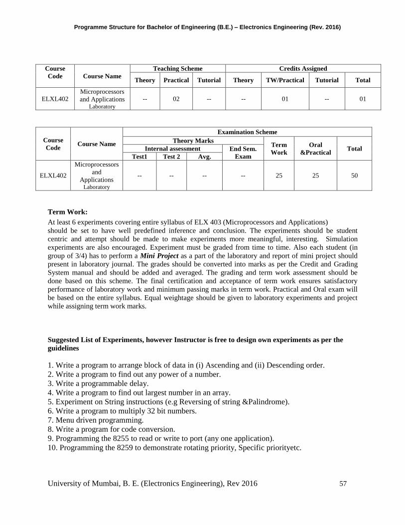
Programme Structure for Bachelor of Engineering (B.E.) – Electronics Engineering (Rev. 2016)
University of Mumbai, B. E. (Electronics Engineering), Rev 2016 57
Course
Code
Course Name
Teaching Scheme Credits Assigned
Theory Practical Tutorial Theory TW/Practical Tutorial Total
ELXL402 Microprocessors
and Applications Laboratory
-- 02 -- -- 01 -- 01
Course
Code Course Name
Examination Scheme
Theory Marks Term
Work
Oral
&Practical Total Internal assessment End Sem.
Exam Test1 Test 2 Avg.
ELXL402
Microprocessors
and
Applications Laboratory
-- -- -- -- 25 25 50
Term Work:
At least 6 experiments covering entire syllabus of ELX 403 (Microprocessors and Applications)
should be set to have well predefined inference and conclusion. The experiments should be student
centric and attempt should be made to make experiments more meaningful, interesting. Simulation
experiments are also encouraged. Experiment must be graded from time to time. Also each student (in
group of 3/4) has to perform a Mini Project as a part of the laboratory and report of mini project should
present in laboratory journal. The grades should be converted into marks as per the Credit and Grading
System manual and should be added and averaged. The grading and term work assessment should be
done based on this scheme. The final certification and acceptance of term work ensures satisfactory
performance of laboratory work and minimum passing marks in term work. Practical and Oral exam will
be based on the entire syllabus. Equal weightage should be given to laboratory experiments and project
while assigning term work marks.
Suggested List of Experiments, however Instructor is free to design own experiments as per the
guidelines
1. Write a program to arrange block of data in (i) Ascending and (ii) Descending order.
2. Write a program to find out any power of a number.
3. Write a programmable delay.
4. Write a program to find out largest number in an array.
5. Experiment on String instructions (e.g Reversing of string &Palindrome).
6. Write a program to multiply 32 bit numbers.
7. Menu driven programming.
8. Write a program for code conversion.
9. Programming the 8255 to read or write to port (any one application).
10. Programming the 8259 to demonstrate rotating priority, Specific priorityetc.

Programme Structure for Bachelor of Engineering (B.E.) – Electronics Engineering (Rev. 2016)
University of Mumbai, B. E. (Electronics Engineering), Rev 2016 58
Course
Code
Course Name
Teaching Scheme Credits Assigned
Theory Practical Tutorial Theory TW/Practical Tutorial Total
ELXL403 Digital System
Design Laboratory
-- 02 -- -- 01 -- 01
Course
Code Course Name
Examination Scheme
Theory Marks Term
Work
Oral
&Practical Total Internal assessment End Sem.
Exam Test1 Test 2 Avg.
ELXL403 Digital System
design Laboratory
-- -- -- -- 25 25 50
Term Work:
At least 6 experiments covering entire syllabus of ELX 404 (Digital System Design)
should be set to have well predefined inference and conclusion. The experiments should be student
centric and attempt should be made to make experiments more meaningful, interesting. Simulation
experiments are also encouraged. Experiment must be graded from time to time. Also each student (in
group of 3/4) has to perform a Mini Project as a part of the laboratory and report of mini project should
present in laboratory journal. The grades should be converted into marks as per the Credit and Grading
System manual and should be added and averaged. The grading and term work assessment should be
done based on this scheme. The final certification and acceptance of term work ensures satisfactory
performance of laboratory work and minimum passing marks in term work. Practical and Oral exam will
be based on the entire syllabus. Equal weightage should be given to laboratory experiments and project
while assigning term work marks.
Suggested List of Experiments, however Instructor is free to design own experiments as per the
guidelines
Experiments based on Hardware: 1. Implementation of Counter using IC 7490, IC 7493
2. Implementation of Synchronous Counter using MSI counter ICs
3. Implementation of Universal Shift Register using IC 74194
4. Design and implement Moore Machine
5. Design and implement Mealy Machine
6. Serial Adder using a Melay/Moore Machine.
7. Design Sequence Detector using FF
Suggested experiments based on software: 1. Implement basic digital logic gates and simulate with HDL.

Programme Structure for Bachelor of Engineering (B.E.) – Electronics Engineering (Rev. 2016)
University of Mumbai, B. E. (Electronics Engineering), Rev 2016 59
2. Implement basic Flip Flops and simulate with HDL.
4. Design and implement full adder logic with HDL and simulate the same.
5. Design and implement multiplexer with HDL and simulate the same.
6. Design and implement multiplexer with HDL and simulate the same.
7. Design and implement decoder (74138) with HDL and simulate the same.
8. Design and implement 4-bit counter with HDL and simulate the same.
9. Design and implement shift register with HDL and simulate the same.
10. Design and simulate the Finite State Machine (FSM) design by HDL.
11. Design and simulate the ALU design by HDL.
Additional suggested experiments (optional) Implementation of any of above using CPLD/FPGA

Programme Structure for Bachelor of Engineering (B.E.) – Electronics Engineering (Rev. 2016)
University of Mumbai, B. E. (Electronics Engineering), Rev 2016 60
Course
Code
Subject Name
Teaching Scheme Credits Assigned
Theory Practical Tutorial Theory TW/Practical Tutorial Total
ELXL404
Principles of
Communication
Engineering Laboratory
-- 02 -- -- 01 -- 01
Subject
Code Subject Name
Examination Scheme
Theory Marks Term
Work
Oral
&Practical Total Internal assessment End Sem.
Exam Test1 Test 2 Avg.
ELXL404
Principles of
Communication
Engineering Laboratory
-- -- -- -- 25 -- 25
Term Work:
At least 6 experiments covering entire syllabus of ELX 405 (Principles of Communication Engineering)
should be set to have well predefined inference and conclusion. The experiments should be student
centric and attempt should be made to make experiments more meaningful, interesting. Simulation
experiments are also encouraged. Experiment must be graded from time to time. Also each student (in
group of 3/4) has to perform a Mini Project as a part of the laboratory and report of mini project should
present in laboratory journal. The grades should be converted into marks as per the Credit and Grading
System manual and should be added and averaged. The grading and term work assessment should be
done based on this scheme. The final certification and acceptance of term work ensures satisfactory
performance of laboratory work and minimum passing marks in term work. Equal weightage should be
given to laboratory experiments and project while assigning term work marks.
Suggested List of Experiments, however Instructor is free to design own experiments as per the
guidelines
1. Amplitude Modulation and demodulation
2. DSB-SC Balanced Modulator
3. Frequency Modulation and Demodulation
4. Super-heterodyne radio receiver
5. Pulse Amplitude Modulation
6. Verification of Sampling Theorem
7. Pulse Width Modulation
8. Pulse Position Modulation
9. Pulse Code Modulation
10. Delta Modulation
11. Adaptive Delta Modulation
12. Time Division Multiplexing