upconversion nanoparticles extending the spectral
TRANSCRIPT

HAL Id: hal-02989880https://hal.archives-ouvertes.fr/hal-02989880
Submitted on 23 Nov 2020
HAL is a multi-disciplinary open accessarchive for the deposit and dissemination of sci-entific research documents, whether they are pub-lished or not. The documents may come fromteaching and research institutions in France orabroad, or from public or private research centers.
L’archive ouverte pluridisciplinaire HAL, estdestinée au dépôt et à la diffusion de documentsscientifiques de niveau recherche, publiés ou non,émanant des établissements d’enseignement et derecherche français ou étrangers, des laboratoirespublics ou privés.
Upconversion nanoparticles extending the spectralsensitivity of silicon photodetectors to λ = 1.5 µ m
Hengyang Xiang, Lei Zhou, Hung-Ju Lin, Zhelu Hu, Ni Zhao, Zhuoying Chen
To cite this version:Hengyang Xiang, Lei Zhou, Hung-Ju Lin, Zhelu Hu, Ni Zhao, et al.. Upconversion nanoparticlesextending the spectral sensitivity of silicon photodetectors to λ = 1.5 µ m. Nanotechnology, Instituteof Physics, 2020, 31 (49), pp.495201. �10.1088/1361-6528/abb2c4�. �hal-02989880�

Upconversion nanoparticles extending the spectral sensitivity of silicon photodetectors to = 1.5 µm
Hengyang Xiang1,3, Lei Zhou2, Hungju Lin3, Zhelu Hu3, Ni Zhao4 and Zhuoying Chen3
1MIIT Key Laboratory of Advanced Display Materials and Devices, Institute of Optoelectronics &
Nanomaterials, College of Materials Science and Engineering, Nanjing University of Science and
Technology, Nanjing 210094, China 2Faculty of Mathematics and Physics, Huaiyin Institute of Technology, Huai׳an 223003, China 3LPEM, ESPCI Paris, PSL Research University, Sorbonne Université, CNRS, 10 Rue Vauquelin, F-
75005 Paris, France 4Department of Electronic Engineering, The Chinese University of Hong Kong, New Territories, Hong
Kong SAR, China
E-mail: [email protected] and [email protected]
Abstract
The telecommunication wavelength of = 1.5 µm has been playing an important role in various fields. In
particular, performing photodetection at this wavelength is challenging, demanding more performance
stability and lower manufacturing cost. In this work, by integrating solution-processed Er3+ doped NaYF4
upconversion nanoparticles (UCNPs) onto a silicon photodetector, UCNPs/Si hybrid photodetectors
(hybrid PDs) are presented. Upon optimization, we demonstrated that a layer of UCNPs can well lead to
an effective spectral sensitivity extension without scarification of the photodetection performance of the
Si photodetector in the visible and near-infrared (near-IR) spectrum. Under the = 1.5 µm illumination, the
hybrid UCNPs/Si-PD exhibits a room-temperature detectivity of 6.15 × 10¹² Jones and a response speed
of 0.4 ms. These UCNPs/Si-PDs represent a promising hybrid strategy towards the quest of low-cost and
broad-band photodetection sensitive from the visible down to the short-wave infrared spectrum.
Keywords: photodetectors, upconversion nanoparticles, short-wave infrared, solution-process

2
1. Introduction
Light sources and photodetection elements operating at a wavelength (λ) of 1.5 µm have been playing a
critical role in various fields, such as optoelectronics [1–3], telecommunications [4], and passive night
vision [5]. At λ = 1.5 µm, the optical loss is lowest in a typical silica fiber, resulting in the wide application
of this wavelength in optical communications [6]. This wavelength is also chosen to enable better-
performing light detection and ranging [7, 8] due to its eye-safe characteristics, allowing a larger detection
range than devices applying illumination in the visible or near-IR spectra [9]. Current photodetector
technologies for λ = 1.5 µm mainly rely on low-bandgap inorganic semiconductors [10], such as indium
gallium arsenide (InGaAs), lead sulfide (PbS), germanium (Ge), indium antimonide (InSb) and mercury
cadmium telluride (HgCdTe). Many of these photodetectors are required to function at low temperatures.
In addition, their fabrication often involves epitaxial growth and highly toxic elements (e.g. arsenic, lead,
mercury, cadmium, and tellurium), causing both cost and ecological issues. In the research into alternative
or next-generation photodetection technologies sensitive to λ = 1.5 µm, various new materials have
emerged including graphene [11–13], MoS2 [14], black phosphorus [15, 16], colloidal PbS nanocrystals
[17, 18], plasmonic nanostructures generating hot carriers [19–21], and colloidal plasmonic nanoparticles
exhibiting strong photothermal effects [20, 21]. Nevertheless, many of these do not completely resolve
both the cost issue due to the highly rigorous nanofabrication processes required (and the low yield of
reproducibility) and the ecological challenges due to the application of highly toxic elements such as lead.
Recently, photon upconversion, the process of converting low-energy photons to high-energy ones, has
been applied as another strategy in pursuit of low-cost alternative photodetection at λ = 1.5 µm. For
example, Zhang et al recently fabricated hybrid photoconductors sensitive to λ = 1.5 µm using organo-
lead hybrid perovskites deposited on top of an erbium silicate nanosheet, resulting in a photoresponsivity
of 0.1 mA W−1 and a rise time of about 900 µs [22]. Solutionprocessed colloidal upconversion
nanoparticles (UCNPs), typically doped by trivalent lanthanide cations, have also shown their high
potential for such applications. Besides the fields of biomedical engineering [23–25] and solar energy
harvesting [26, 27], they have also been applied to photodetection [28, 29]. Working on photodetectors
sensitive to the wavelength of 1.5 µm, Zhao and co-workers recently fabricated flexible photoconductors
by mixing Er3+-doped UCNPs with conjugated polymer [28]. Despite the interesting demonstration, the
response speed of these photoconductors was not well characterized. By using a photodiode structure, we
have recently demonstrated solution-processed flexible polymer/UCNP hybrid photodetectors exhibiting
a responsivity of 0.73 mA W−1 and a rise time of 80 µs [29]. In these conjugated polymer/UCNP hybrid
3
photodetectors, while the inorganic UCNPs are highly stable in air, the air stability of the conjugated
polymer remains modest. By comparison, an allinorganic configuration should in principle exhibit
advantages. In this work, we propose an all-inorganic hybrid photodetector (hybrid PD) sensitive to λ =
1.5 µm employing a layer of solution-processed colloidal Er3+-doped NaYF4 UCNPs on a silicon
photodetector. In such a configuration, the UCNPs absorb λ = 1.5 µm photons and upconvert them into
fluorescence falling in the visible and the near-IR spectrum (at λ = 520 nm, 545 nm, 650 nm, 810 nm, and
980 nm), which is subsequently harvested by the Si photodetector resulting in photocurrent generation. In
an optimized UCNP/Si hybrid PD, a high photoresponsivity of more than 10 mA W−1 and a room-
temperature detectivity of 6.15 × 10¹² Jones, together with a rise time as low as 430 µs were achieved
under λ = 1.5 µm illumination. The results reported here represent a more than ten-fold enhancement in
terms of photoresponsivity by comparison to previous works applying Er3+-doped upconversion materials
on hybrid lead perovskites [22] or on conjugated polymers [29]. The room-temperature detectivity of 6.15
× 1012 Jones obtained by the work under λ = 1.5 µm illumination suggests a strong competitiveness of
these UCNPs/Si hybrid PDs by comparison to commercial PDs sensitive at this wavelength [10]. The
current UCNPs/Si hybrid PDs described here thus pave a new path towards low-cost and broadband
photodetection sensitive in the spectrum from visible light down to the short-wave infrared.
2. Experimental section
2.1. Synthesis method of Er3+-doped NaYF4 UCNPs
A hydrothermal route [29, 30] was used for the synthesis of the Er3+-doped NaYF4 UCNPs in this work.
Firstly, three aqueous solutions were prepared by adding Ln(NO3)3 · 6H2O (0.2 mol l−1 ), sodium citrate
tribasic dihydrate (0.6 mol l−1 ), and sodium fluoride (NaF, 2.4 mol l−1 ) to 5 ml of deionized (DI) water,
named solution A, solution B and solution C, respectively. For solution A, the Ln3+ contained Y3+ and Er3+
with a Y3+/Er3+ molar ratio of 85:15. Solutions A and B were then mixed together with vigorous stirring
to form a lanthanide citrate. Solution C was subsequently slowly added into the above mixture and the
final solution was stirred for 1 h. Afterwards, this final solution was transferred into an autoclave for
hydrothermal treatment in an oven at 120 ◦C for a duration of 2 h. The autoclave was then taken out of the
oven and allowed to cool to room temperature naturally (overnight). A centrifugation (6000 rpm, 30 min)
process was used to separate the UCNPs from the solution. The UCNPs were then washed several times
in DI water. Finally, the UCNPs were dried in a vacuum (60 ◦C, 24 h) and subsequently annealed in air
(300 ◦C, 2 h).
2.2. Device preparation and characterization

4
A Si PD (LSSPD-1.2) was obtained from Beijing Lightsensing Technologies Ltd (a 1.2 mm Silicon PIN
photodiode, size: 1.2 mm × 1.2 mm). The UCNPs were firstly dispersed in isopropanol (IPA) by
ultrasonication. The concentrations for UCNPs-1, UCNPs-2 and UCNPs-3 were 20 g l−1 , 30 g l−1 and 40
g l−1 , respectively. To prepare the UCNP/Si PDs, 60 µl of UCNP solution was drop-coated onto the
surface of the Si photodetector. For photoresponsivity measurement in the λ = 350 nm–1650 nm spectrum
window, monochromatic light was generated by a tungsten halogen lamp coupled with a monochromator
(Oriel Cornerstone 130); the emission characteristic of the tungsten halogen lamp is shown in figure S1
of the supplementary material. This monochromatic light was then modulated by a mechanical chopper
(SR540, Stanford Research Systems. Inc.) with its modulation frequency adjustable from 4 Hz to 3.7 kHz.
During our experiments, a modulation frequency of 17 Hz was applied, with the chopper placed between
the light source and the photodetector under study. The short-circuit current of the photodetector was
measured by a computer-controlled Keithley 2612B SourceMeter® instrument (with an applied voltage
of 0 V). NIST-calibrated Si and Ge cells were used as references to calibrate the monochromatic
illumination power at every wavelength. For the power-dependent and time-dependent photoresponse
characteristics, the hybrid PDs were illuminated by a laser at λ = of 1.5 µm, modulated by a function
generator. The photocurrent was converted by a low-noise current preamplifier (SR570) into a voltage
signal which was monitored by a digital oscilloscope (Tektronix DPO2024B). All device measurements
were performed in air at room temperature.
2.3. Material characterizations
SEM images of the UCNPs were obtained by a FEI Magellan 400 system with a standard field emission
gun source. Powder x-ray powder diffraction (XRD) spectra were obtained by a PANalytical X’Pert x-ray
diffractometer using Cu-Kα radiation. The optical absorption was measured in air by an Agilent Cary 5E
UV–vis/near-IR spectrometer. The steadystate fluorescence of the UCNPs was recorded by an Ocean
Optics spectrometer (HR4000) while the sample (UCNPs) was excited by a laser diode (LPSC-1550-FC,
center wavelength: 1537 nm). For time-resolved fluorescence, the UCNPs were first deposited onto a
microscopy glass slide. The fluorescence was recorded using a tunable optical parametric oscillator
pumped by a tunable Ekspla S-7NT342B OPO laser with a 7 ns pulse duration at 1540 nm. A CCD camera
(Princeton Instruments) equipped with a monochromator (Acton Research, 300 lines mm−1 ) was used to
measure the fluorescence spectra. An RCA 8850 photomultiplier was used to detect the decay curves. All
measurements were performed at room temperature.
3. Results and discussion

5
Figure 1. (a) Transmission electron microscopy (TEM) image of Er3+-doped NaYF4 UCNPs. (b) X-ray
powder diffraction (XRD) pattern of the UCNPs plotted together with the reference pattern (JCPDS no.
00-016-0334). (c) The upconversion fluorescence spectrum of the UCNPs (the red dotted curve) under a
laser excitation at λ = 1.5 µm (power = 10 mW). The absorbance spectra of Si is shown as the black curve.
(d) Schematic illustrating the energy transitions corresponding to the upconversion fluorescence observed
under the excitation of a λ = 1.5 µm laser. GSA = ground-state absorption, ESA = excited-state absorption.
The solution-processed colloidal Er3+-doped NaYF4 UCNPs were synthesized by a hydrothermal method
according to a previously described protocol [29, 30]. The UCNPs applied in this work have an average
diameter of 450 nm (Figure 1(a)). A hexagonal β phase, a crystal structure which generally allows for a
stronger fluorescence than the cubic phase [31], was determined by XRD to be present in these UCNPs
(Figure 1(b)). When Er3+-doped NaYF4 UCNPs are excited by a λ = 1.5 µm laser, the incident photons are
absorbed by the Er3+ cation, either through ground-state absorption or excitedstate absorption (see the
schematic shown in Figure 1(d)). The upconversion process, which converts lower-energy incoming
photons into higher-energy outgoing photons by fluorescence, typically involves a multiphoton absorption
mechanism followed by relaxation, de-excitation, and emission [32, 33]. For example, the fluorescence
emissions of Er3+- doped NaYF4 UCNPs at λ = 520 nm, 545 nm and 650 nm require a three-photon
absorption process, while the fluorescence at λ = 810 nm and 980 nm involves a two-photon absorption
process. Even with laser excitation at a relatively low power (10 mW), a bright greenish fluorescence can
be observed by the naked eye, as shown in the inset picture in Figure 1(c). By a reported method employing
an integrating sphere [34], a fluorescence quantum yield of about 2.5% was determined to have been
6
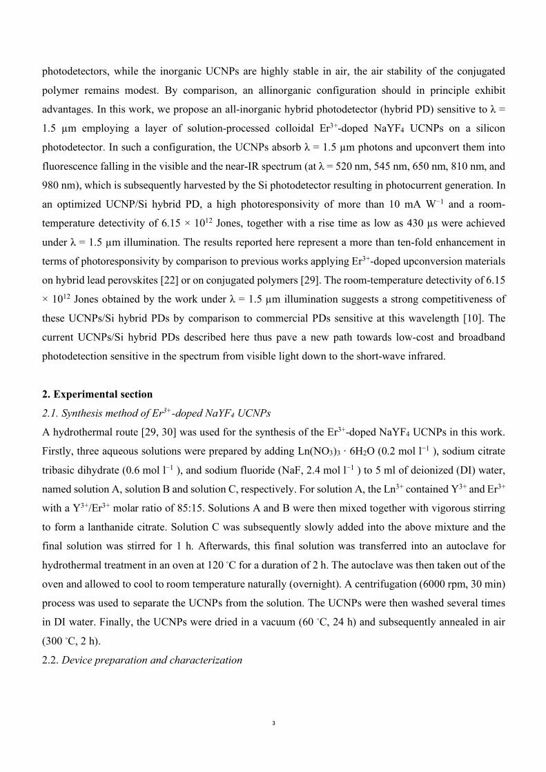
achieved by these UCNPs. As the absorption spectrum of Si easily covers all the upconverted fluorescence
(the black curve in Figure 1(c)), these results suggest that the UCNPs decribed here can effectively
upconvert λ = 1.5 µm photons into fluorescence harvestable by Si.
Figure 2. (a) Schematic describing the device architecture of the UCNP/Si hybrid PD. (b) Scanning
electron microscope (SEM) image of the UCNP layer of an optimized hybrid PD. The zoom-in SEM
image of this layer is shown on the right. (c) A picture of the hybrid PD under the illumination of a λ =
1.5 µm laser.
UCNPs were then dispersed in isopropanol giving a concentration ranging from 20 to 40 mg ml−1. These
UCNP solutions were then drop-cast onto the surface of a commercial Si photodetector (Beijing
Lightsensing Technologies Ltd, LSSPD-1.2, size: 1.2 mm by 1.2 mm). The resultant UCNP film thickness
was tunable by varying the concentration of the solution. A schematic of these UCNP/Si hybrid PDs is
shown in Figure 2(a). UCNP layers of different thickness were loaded on the Si photodetector with the
majority of the nanoparticle layer corresponding to zero to two monolayers with visible empty areas, or
one to two monolayers, or more than two monolayers, which will be referred to below as UCNPs-1,
UCNPs-2 and UCNPs-3, respectively. In an optimized hybrid device, the UCNPs form a relatively
homogenous layer, with a thickness of less than 2 layers of nanoparticles (UCNPs-2, Figure 2(b). SEM
images of UCNPs-1 and UCNPs-3 are shown in Figure S2 of the supplementary material), covering the
Si photodetector and performing upconversion of λ = 1.5 µm photons to photons harvestable by Si. To
verify the uniformity of the UCNP film and its influence on photodetection, a smaller laser spot (~ 0.4
mm in diameter) was focused onto different areas of the UCNP/Si hybrid PD surface, which is shown in

7
Figure S3 of the supplementary material. Three measurements were performed under identical
illumination in each sample area and the results showed only a small photocurrent fluctuation (< ±10%)
owing to the inhomogeneity of the UCNP film (Figure S3 of supplementary material). In addition, as such
a UCNP film has little impact on the visible light transmittance of the Si device underneath (Figure 2(c)
and Figure S4 of the supplementary material), the hybrid device was able to retain an almost identical
photodetection capability for visible and near-IR photons by comparison with a bare Si photodetector
(without the UCNP layer), enabling a broadband photodetection characteristic for the hybrid detector.
Figure 3. Photoresponsivity as a function of incident wavelengths from 400 nm to 1650 nm. The insert
figure shows the zoom-in responsivity in the wavelength range from 400 nm to 1200 nm.
The photoresponsivities of these UCNP/Si hybrid PDs as a function of incident photon wavelengths from
350 nm to 1650 nm were characterized under monochromatic illumination obtained from a quartz tungsten
halogen light source coupled with a monochromator (Figure 3). Concerning the visible/near-IR spectrum
(400–1100 nm), including the bare Si photodetector without any UCNPs (called ‘blank Si-PD’), all
devices tested showed a clear photoresponse. Loading a significant amount of UCNPs in this hybrid device
configuration (e.g. UCNPs-3) can result in a negative impact on the photodetection capability of the Si
device in the visible/near-IR spectrum due to the optical absorption of UCNPs. Nevertheless, as shown in
the insert of Figure 3, when a moderate amount of UCNPs were applied (e.g. UCNPs-1 and UCNPs-2
configurations), only a slight decrease (<3% @ 950 nm) of photoresponsivity in the visible/near-IR
spectrum was found in the hybrid devices by comparison to the blank Si-PD. Concerning photons with a
wavelength longer than 1100 nm, as expected from the bandgap of Si, the photoresponsivity of the blank
Si-PD starts to drop drastically reaching ~3 × 10⁻⁵ A W−1 at λ > 1200 nm. By comparison, in the spectrum
window 1400 nm < λ < 1700 nm, UCNP/Si hybrid PDs exhibited a much higher photoresponsivity,
reaching a maximum of 0.008 A W−1 at λ = 1.55 µm, which corresponds to >100 times higher than that of

8
a blank Si-PD. Comparing the hybrid PDs with different amounts of UCNP loading, there was a clear
increase of photoresponsivity at λ = 1.5 µm from UCNPs-1 to UCNPs-2 while such an increase became
very small when more UCNPs were loaded (in UCNPs-3). This can be understood as the consequence of
increased self absorption of the upconverted fluorescence when many layers of UCNPs were loaded on
top of the Si device leading only to a mild increase of photoresponsivity from 0.008 A W−1 to 0.009 A
W−1 at 1550 nm when changing the loading from UCNPs-2 to UCNPs-3. When considering the
photoresponsivity in the whole spectrum window, the UCNPs-2/Si hybrid PD can offer a trade-off
between the increase of photoresponsivity at around λ = 1.5 µm without much sacrifice of
photoresponsivity in the visible/near-IR spectrum.
Figure 4. (a) Time-dependent photocurrent (applied voltage = 0 V) of an UCNPs-2/Si-PD under the
illumination of a λ = 1.5 µm laser at different laser powers. (b) The responsivity/ detectivity of this
UCNPs/Si-PD as a function of incident laser power. (c) Time-dependent photoresponse. (d) A zoom-in
view of the time-dependent photoresponse from Figure 4c with the measured device rise/fall time (Trise =
rise time, and Tfall = fall time).
A λ = 1.5 µm laser was then focused (spot diameter ∼1.0 mm) onto the surface of a UCNPs-2/Si hybrid
PD to further study its time-dependent and power-dependent room-temperature photoresponse
characteristics. A series of laser powers ranging from 0.05 µW to 0.2 mW were used in the experiment. A
clear photoresponse in terms of the photocurrent (A) following the laser being powered on/off can be
observed at different laser powers (Figure 4(a)). These data allow us to obtain the evolution of the
responsivity/detectivity over different laser powers under λ = 1.5 µm illumination (Figure 4(b)), which
9
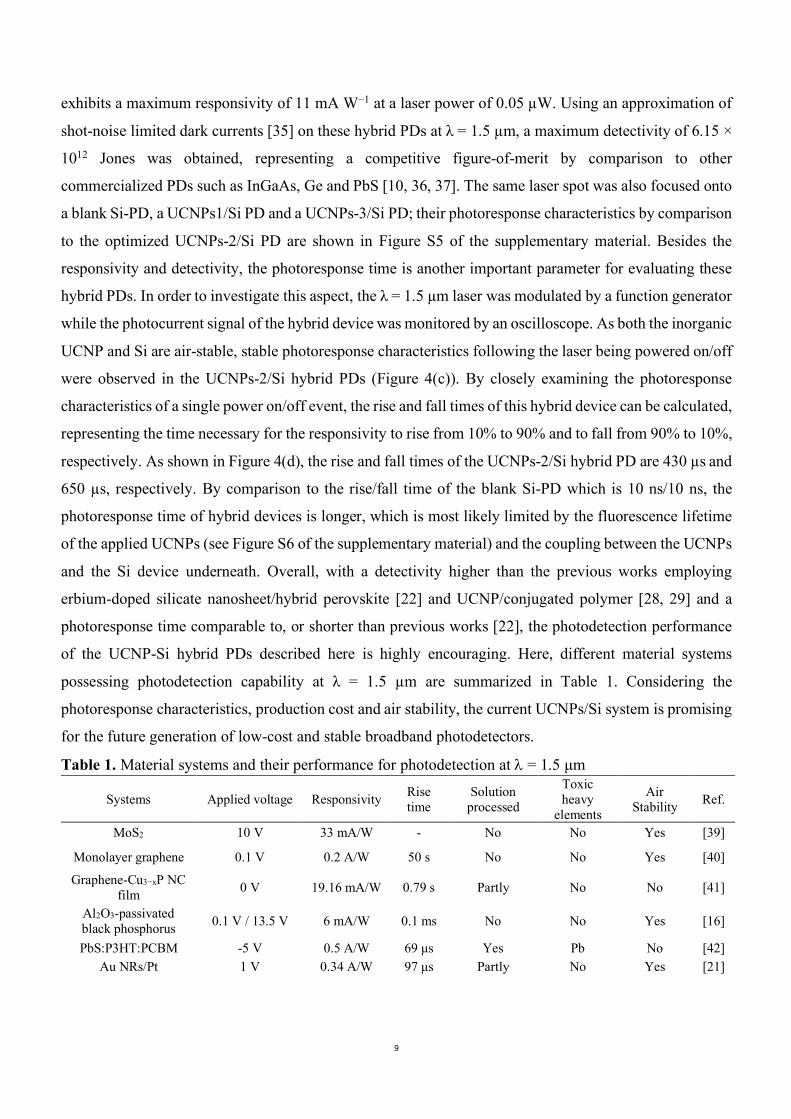
exhibits a maximum responsivity of 11 mA W−1 at a laser power of 0.05 µW. Using an approximation of
shot-noise limited dark currents [35] on these hybrid PDs at λ = 1.5 µm, a maximum detectivity of 6.15 ×
1012 Jones was obtained, representing a competitive figure-of-merit by comparison to other
commercialized PDs such as InGaAs, Ge and PbS [10, 36, 37]. The same laser spot was also focused onto
a blank Si-PD, a UCNPs1/Si PD and a UCNPs-3/Si PD; their photoresponse characteristics by comparison
to the optimized UCNPs-2/Si PD are shown in Figure S5 of the supplementary material. Besides the
responsivity and detectivity, the photoresponse time is another important parameter for evaluating these
hybrid PDs. In order to investigate this aspect, the λ = 1.5 µm laser was modulated by a function generator
while the photocurrent signal of the hybrid device was monitored by an oscilloscope. As both the inorganic
UCNP and Si are air-stable, stable photoresponse characteristics following the laser being powered on/off
were observed in the UCNPs-2/Si hybrid PDs (Figure 4(c)). By closely examining the photoresponse
characteristics of a single power on/off event, the rise and fall times of this hybrid device can be calculated,
representing the time necessary for the responsivity to rise from 10% to 90% and to fall from 90% to 10%,
respectively. As shown in Figure 4(d), the rise and fall times of the UCNPs-2/Si hybrid PD are 430 µs and
650 µs, respectively. By comparison to the rise/fall time of the blank Si-PD which is 10 ns/10 ns, the
photoresponse time of hybrid devices is longer, which is most likely limited by the fluorescence lifetime
of the applied UCNPs (see Figure S6 of the supplementary material) and the coupling between the UCNPs
and the Si device underneath. Overall, with a detectivity higher than the previous works employing
erbium-doped silicate nanosheet/hybrid perovskite [22] and UCNP/conjugated polymer [28, 29] and a
photoresponse time comparable to, or shorter than previous works [22], the photodetection performance
of the UCNP-Si hybrid PDs described here is highly encouraging. Here, different material systems
possessing photodetection capability at λ = 1.5 µm are summarized in Table 1. Considering the
photoresponse characteristics, production cost and air stability, the current UCNPs/Si system is promising
for the future generation of low-cost and stable broadband photodetectors.
Table 1. Material systems and their performance for photodetection at l = 1.5 µm
Systems Applied voltage Responsivity Rise time
Solution processed
Toxic heavy
elements
Air Stability Ref.
MoS2 10 V 33 mA/W - No No Yes [39]
Monolayer graphene 0.1 V 0.2 A/W 50 s No No Yes [40]
Graphene-Cu3−xP NC film 0 V 19.16 mA/W 0.79 s Partly No No [41]
Al2O3-passivated black phosphorus 0.1 V / 13.5 V 6 mA/W 0.1 ms No No Yes [16]
PbS:P3HT:PCBM -5 V 0.5 A/W 69 µs Yes Pb No [42] Au NRs/Pt 1 V 0.34 A/W 97 µs Partly No Yes [21]

10
Perovskite-erbium silicate 1 V 0.1 mA/W 0.9 ms No Pb No [22]
Erbium chloride borate - CdS nanoribbon
5 V 0.2 mA/W 44 ms Partly Cd No [34]
Erbium-doped-UCNPs:pDPPT-TT:
PCBM 0 V 0.73 mA/W 80 µs Yes No No [29]
Erbium-doped-UCNPs:Si-PD 0 V 11 mA/W 0.43 ms Partly No Yes This
work
4. Conclusions
In summary, in this work we have proposed an alternative but feasible strategy for λ = 1.5 µm
photodetection by the formation of nanoparticle/Si hybrid photodetectors employing solution-processed
colloidal UCNPs. These UCNPs/Si hybrid PDs effectively expand the spectrum response of Si up to λ =
1.7 µm while maintaining the photodetection capability of Si in the visible/near-IR spectrum. At λ = 1.5
µm, the optimized UCNPs/Si hybrid PDs exhibited a high responsivity of 11 mA W−1 , a maximum room-
temperature detectivity of 6.15 × 10¹² Jones, and a photoresponse time of 0.4 ms. Considering the
simplicity of the device’s structure and the adaptability of colloidal nanoparticles to large-scale solution
processes, the UCNPs/Si hybrid PDs described pave a new path to the future generation of low-cost, stable,
and broadband room-temperature photodetectors sensitive to visible, near-IR and short-wave IR photons.
Acknowledgments
The SEM characterizations performed were supported by the region of Ile-de-France in the framework of
DIM Nano-K. H X acknowledges the Postdoctoral Research Funding Scheme of Jiangsu Province (No.
2020Z124). H X and Z H acknowledge the China scholarship council (CSC) for their Ph.D. thesis
scholarships. N Z and Z C acknowledge the PHC PROCORE project (No. 31041VL). L Z acknowledges
financial support from the National Natural Science Foundation of China (Grant No. 61775076), the
project of the Six Talent Peaks of Jiangsu Province (Grant No. DZXX-011), the Natural Science Funding
for Colleges and Universities in Jiangsu Province (Grant No.18KJD140001), the Qinglan project of
Jiangsu Province and ‘333 High-level Talents Training Program’ of Jiangsu Province.
References
[1] Eng P W U, Hou Q I Z, Ang Y U W, Eng G U D, An Y U F, Hen S I S, Iang Q X U, Ang Y U W, Ong
H A S and Ang Y O U W 2019 Wavelength-tunable passively mode-locked all-fiber laser at 1.5 µm Appl.
Opt. 58 5143–7
11
[2] Zeng M, Artizzu F, Liu J, Singh S, Locardi F, Mara D, Hens Z and Van Deun R 2020 Boosting the
Er3+ 1.5 µm luminescence in CsPbCl3 perovskite nano-crystals for photonic devices operating at
telecommunication wavelengths ACS Appl. Nano Mater. 3 4699–707
[3] Leong D, Harry M, Reeson K J and Homewood K P 1997 A silicon/iron-disllicide light-emitting diode
operating at a wavelength of 1.5 µm Nature 387 686–8
[4] Ho V X, Wang Y, Ryan B, Patrick L, Jiang H X, Lin J Y and Vinh N Q 2020 Observation of optical
gain in Er-Doped GaN epilayers J. Lumin. 221 1–5
[5] Steinvall O 2013 Active and passive imaging NIR/SWIR performance for slant paths close to ground
Opt. InfoBase Conf. Pap. 52 4763–78
[6] Wartak M S 2013 Introduction Computational Photonics: An Introduction with MATLAB (Cambridge:
Cambridge University Press) pp 1–16
[7] Bronstein H et al 2011 Thieno[3,2-b]thiophene− diketopyrrolopyrrole-containing polymers for high-
performance organic field-effect transistors and organic photovoltaic devices J. Am. Chem. Soc. 133 3272
[8] Hecht J 2018 Lidar for self-driving cars Opt. Photonics News 29 26–33
[9] Myers M J, Myers J D, Sarracino J T, Hardy C R, Guo B, Christian S M, Myers J A, Roth F and Myers
A G 2010 LIBS system with compact fiber spectrometer, head mounted spectra display and hand held
eye-safe erbium glass laser gun Proc. SPIE 7578 75782G
[10] Zeller J W, Efstathiadis H, Bhowmik G, Haldar P, Dhar N K, Lewis J, Wijewarnasuriya P, Puri Y R
and Sood A K 2015 Development of Ge PIN photodetectors on 300 mm Si wafers for near-infrared sensing
Int. J. Eng. Res. Technol. 8 23-33
[11] Xia F, Mueller T, Lin Y, Valdes-Garcia A and Avouris P 2009 Ultrafast graphene photodetector Nat.
Nanotechnol. 4 839
[12] Pospischil A, Humer M, Furchi M M, Bachmann D, Guider R, Fromherz T and Mueller T 2013
CMOS-compatible graphene photodetector covering all optical communication bands Nat. Photon. 7 892
[13] Chen Z, Li X, Wang J, Tao L, Long M, Liang S J, Ang L K, Shu C, Tsang H K and Xu J B 2017
Synergistic effects of plasmonics and electron trapping in graphene short-wave infrared photodetectors
with ultrahigh responsivity ACS Nano 11 430–7
[14] Xie Y et al 2017 Ultrabroadband MoS2 photodetector with spectral response from 445 to 2717 nm
Adv. Mater. 29 1605972
[15] Du H, Lin X, Xu Z and Chu D 2015 Recent developments in black phosphorus transistors J. Mater.
Chem. C 3 8760–75

12
[16] Na J, Park K, Kim J T, Choi W K and Song Y W 2017 Air-stable few-layer black phosphorus
phototransistor for near-infrared detection Nanotechnology 28 085201
[17] Kufer D, Nikitskiy I, Lasanta T, Navickaite G, Koppens F H L and Konstantatos G 2015 Hybrid 2D-
0D MoS2-PbS quantum dot photodetectors Adv. Mater. 27 176–80
[18] Saran R and Curry R J 2016 Lead sulphide nanocrystal photodetector technologies Nat. Photon. 10
81
[19] Sobhani A, Knight M W, Wang Y, Zheng B, King N S, Brown L V,, Fang Z, Nordlander P and Halas
N J 2013 Narrowband photodetection in the near-infrared with a plasmon-induced hot electron device Nat.
Commun. 4 1643
[20] Xiang H, Niu T, Schoenauer Sebag M, Hu Z, Xu X, Billot L, Aigouy L and Chen Z 2018 Short-wave
infrared sensor by the photothermal effect of colloidal gold nanorods Small 14 1704013
[21] Xiang H, Hu Z, Billot L, Aigouy L and Chen Z 2019 Hybrid plasmonic gold-nanorod–platinum short-
wave infrared photodetectors with fast response Nanoscale 11 18124–31
[22] Zhang X et al 2017 Perovskite–erbium silicate nanosheet hybrid waveguide photodetectors at the
near-infrared telecommunication band Adv. Mater. 29 1604431
[23] Idris N M, Jayakumar M K G, Bansal A and Zhang Y 2015 Upconversion nanoparticles as versatile
light nanotransducers for photoactivation applications Chem. Soc. Rev. 44 1449–78
[24] Wang F, Banerjee D, Liu Y, Chen X and Liu X 2010 Upconversion nanoparticles in biological
labeling, imaging, and therapy Analyst 135 1839–54
[25] Sedlmeier A and Gorris H H 2015 Surface modification and characterization of photon-upconverting
nanoparticles for bioanalytical applications Chem. Soc. Rev. 44 1526–60
[26] Goldschmidt J C and Fischer S 2015 Upconversion for photovoltaics – a review of materials, devices
and concepts for performance enhancement Adv. Opt. Mater. 3 510–35
[27] Schoenauer Sebag M, Hu Z, de Oliveira Lima K, Xiang H, Gredin P, Mortier M, Billot L, Aigouy L
and Chen Z 2018 Microscopic evidence of upconversion-induced near-infrared light harvest in hybrid
perovskite solar cells ACS Appl. Energy Mater. 1 3537–43
[28] Zhao X, Song L, Zhao R and Tan M C 2019 High-performance and flexible shortwave infrared
photodetectors using composites of rare earth-doped nanoparticles ACS Appl. Mater. Interfaces 11 2344–
51
[29] Xiang H, Hu Z, Billot L, Aigouy L, Zhang W, McCulloch I and Chen Z 2019 Heavy-metal-free
flexible hybrid polymer-nanocrystal photodetectors sensitive to 1.5 µm wavelength ACS Appl. Mater.
Interfaces 11 42571–9

13
[30] Zhao J, Sun Y, Kong X, Tian L, Wang Y, Tu L, Zhao J and Zhang H 2008 Controlled synthesis,
formation mechanism, and great enhancement of red upconversion luminescence of NaYF4: Yb3+,Er3+
nanocrystals/submicroplates at low doping level J. Phys. Chem. B 112 15666–72
[31] Liu D, Jing Y, Wang K, Wang Y and Luo G 2019 Reaction study of α-phase NaYF4:Yb,Er generation
via a tubular microreactor: discovery of an efficient synthesis strategy Nanoscale 11 8363–71
[32] Zhang Y, Li S, Qin F, Zhang Z and Dai Z 2015 Ultraviolet and visible upconversion luminescence
in Y2O3:Er3+, Gd3+ microcrystals by 155 µm excitation J. Opt. Soc. Am. B 32 1856
[33] Fu Y, Qi Z, Xu X, Li L, Wang X, Zhu X, Zhuang X and Pan A 2019 Near-infrared photodetection
based on erbium chloride borate nanobelts Appl. Phys. Express 12 035001
[34] Faulkner D O, Mcdowell J J, Price A J, Perovic D D, Kherani N P and Ozin G A 2012 Measurement
of absolute photoluminescence quantum yields using integrating spheres - Which way to go? Laser
Photonics Rev. 6 802–6
[35] Dou L, Yang Y M, You J, Hong Z, Chang W H, Li G and Yang Y 2014 Solution-processed hybrid
perovskite photodetectors with high detectivity Nat. Commun. 5 1–6
[36] Rogalski A 2012 Progress in focal plane array technologies Prog. Quantum Electron. 36 342–473
[37] Conley B R et al 2014 Si based GeSn photoconductors with a 1.63 A W−1 peak responsivity and a
2.4 µm long-wavelength cutoff Appl. Phys. Lett. 105 221117
[38] Zhang B Y, Liu T, Meng B, Li X, Liang G, Hu X and Wang Q J 2013 Broadband high photoresponse
from pure monolayer graphene photodetector Nat. Commun. 4 1811
[39] Sun T et al 2017 Flexible broadband graphene photodetectors enhanced by plasmonic Cu3−xP
colloidal nanocrystals Small 13 1–9
[40] Rauch T, Böberl M, Tedde S F, Fürst J, Kovalenko M V, Hesser G, Lemmer U, Heiss W and Hayden
O 2009 Near-infrared imaging with quantum-dot-sensitized organic photodiodes Nat. Photon. 3 332–6

14