usb224x data sheet - microchip technology · 2015. 8. 3. · 2010 - 2015 microchip technology inc....
TRANSCRIPT
USB224XUltra Fast USB 2.0 Multi-Format, SD/MMC, and MS Flash
Media Controllers
HighlightsThe Microchip USB224x is a USB 2.0 compliant, Hi-Speed bulk only1 mass storage class peripheral con-troller intended for reading and writing to popular flashmedia from the xD-Picture CardTM (xD)2, MemoryStick® (MS), Secure Digital (SD), and MultiMedia-CardTM (MMC) families.
The USB224x is a fully integrated, single chip solutioncapable of ultra high performance operation. Averagesustained transfer rates exceeding 35 MB/s are possi-ble if the media and host can support those rates. TheUSB2244/44i includes provisions to read/write securemedia formats.
General Features
• Low pin count 36-pin QFN (6x6 mm) RoHS com-pliant package
• USB2240/40I/41/41I- Targeted for applications in which single or
"combo" media sockets are used• Hardware-controlled data flow architecture for all
self-mapped media• Pipelined hardware support for access to non-
self-mapped media• Order number with “I” denote the products that
support the industrial temperature range of -40ºC to 85ºC
• Support included for secure media format on a licensed, customized basis- USB2244/44I: SD Secure
Hardware Features
• Single chip flash media controller with- USB2240/40I/41/4I: multiplexed interface for
use with “combo” card sockets- USB2244/44I: SD/MMC flash media reader/
writer• MMC Streaming Mode support• Extended configuration options
- xD player mode operation - Socket switch polarities, etc.
• Media Activity LED• On board 24 MHz crystal driver circuit• Optional external 24 MHz clock input3
• Internal card power FET- 200 mA - "Fold-back" short circuit protection
• 8051 8-bit microprocessor- 60 MHz - single cycle execution- 64 KB ROM | 14 KB RAM
• Supports a single external 3.3 V supply source; internal regulators provide 1.8 V internal core volt-age for additional bill of materials and power sav-ings
• Optimized pinout improves signal routing which eases implementation for improved signal integ-rity
Flash Media Specification Compliance
• Secure Digital 2.0- HS-SD, SDHC - TransFlashTM and reduced form factor media
• MultiMediaCard 4.2- 1/4/8-bit MMC
• Memory Stick Formats - MS 1.43, Pro 1.02, Duo 1.10 - Pro-HG Duo 1.01
–MS, MS Duo, HS-MS, MS Pro-HG, MS Pro• xD-Picture Card 1.2
Software Features
• Customizable vendor specific data• Optimized for low latency interrupt handling• Reduced memory footprint
Applications
• Flash media card reader/writers• Desktop and mobile PCs • Printers• Consumer A/V and media players/viewers• Compatible with
–Microsoft® VistaTM and Vista ReadyBoostTM
–Windows® XP, ME, 2K SP4–Apple Mac OSx®
–Linux Mass Storage Class Drivers
1.Bulk only is not applicable to USB2240/40i/41/41i.2.xD-Picture Card is not applicable to USB2241/41i. 3.Only applicable to USB2240/40i/41/41i.
2010 - 2015 Microchip Technology Inc. DS00001979A-page 1

USB224X
TO OUR VALUED CUSTOMERS
It is our intention to provide our valued customers with the best documentation possible to ensure successful use of your Microchipproducts. To this end, we will continue to improve our publications to better suit your needs. Our publications will be refined andenhanced as new volumes and updates are introduced.
If you have any questions or comments regarding this publication, please contact the Marketing Communications Department viaE-mail at [email protected]. We welcome your feedback.
Most Current Data SheetTo obtain the most up-to-date version of this data sheet, please register at our Worldwide Web site at:
http://www.microchip.com
You can determine the version of a data sheet by examining its literature number found on the bottom outside corner of any page. The last character of the literature number is the version number, (e.g., DS30000000A is version A of document DS30000000).
ErrataAn errata sheet, describing minor operational differences from the data sheet and recommended workarounds, may exist for cur-rent devices. As device/documentation issues become known to us, we will publish an errata sheet. The errata will specify therevision of silicon and revision of document to which it applies.
To determine if an errata sheet exists for a particular device, please check with one of the following:• Microchip’s Worldwide Web site; http://www.microchip.com• Your local Microchip sales office (see last page)
When contacting a sales office, please specify which device, revision of silicon and data sheet (include -literature number) you areusing.
Customer Notification SystemRegister on our web site at www.microchip.com to receive the most current information on all of our products.
DS00001979A-page 2 2010 - 2015 Microchip Technology Inc.
2010 - 2015 Microchip Technology Inc. DS00001979A-page 3
USB224X
1.0 INTRODUCTION
The Microchip USB224x is a flash media card reader solution fully compliant with the USB 2.0 specification. All requiredresistors on the USB ports are integrated into the device. This includes all series termination resistors on D+ and D–pins and all required pull-down and pull-up resistors. The over-current sense inputs for the downstream facing portshave internal pull-up resistors.
1.1 Hardware Features
• Single chip flash media controller in low pin count 36-pin QFN, RoHS compliant package
• Commercial temperature products support 0°C to +70°C: USB2240/41 and USB2244
• Industrial temperature products support -40°C to +85°C: USB2240I/41I and USB2244I
• 8051 8-bit microprocessor
- 60 MHz - single cycle execution
- 64 KB ROM |14 KB RAM
• Supports a single external 3.3 V supply source; internal regulators provide 1.8 V internal core voltage for addi-tional bill of materials and power savings
Compliance with the following flash media card specifications:
• Secure Digital 2.0
- HS-SD and SDHC
- TransFlash™ and reduced form factor media
• MultiMediaCard 4.2
- 1/4/8 bit MMC
• Memory Stick 1.43
• Memory Stick Pro Format 1.02
• Memory Stick Pro-HG Duo Format 1.01
- Memory Stick, MS Duo, HS-MS, MS Pro-HG, MS Pro
• Memory Stick Duo 1.10
• xD-Picture Card 1.2
1.2 Software Features
• If the OEM is using an external EEPROM, the following features are available:
- Customizable vendor, product, language, and device ID’s
- 12-hex digits maximum for the serial number string
- 28-character manufacturer ID and product strings for the flash media reader/writer
- LED blink interval or duration
USB224X
DS00001979A-page 4 2010 - 2015 Microchip Technology Inc.
2.0 ACRONYMS
ATA: Advanced Technology Attachment
FET: Field Effect Transistor
LUN: Logical Unit Number
MMC: MultiMediaCard
MSC: Memory Stick Controller1
PLL: Phase-Locked Loop
QFN: Quad Flat No leads
RoHS: Restriction of Hazardous Substances Directive
RXD: Received eXchange Data
SDC: Secure Digital Controller
SIE: Serial Interface Engine
TXD: Transmit eXchange Data
UART: Universal Asynchronous Receiver-Transmitter
UCHAR: Unsigned Character
UINT: Unsigned Integer
1.Not applicable to USB2244/44i.

USB224X
3.0 BLOCK DIAGRAMS
FIGURE 3-1: USB2240/40I/41/41I BLOCK DIAGRAM
FMDUCTL
8051
PROCESSOR
SFR RAM
MS
RAM
USB Host
AUTO_CBW PROC
PHYFMI
XDATA BRIDGE+ BUS ARBITER
BUS INTFC
BUS INTFC
BUS INTFC
EP0 TXEP0 RX
EP2 TXEP2 RX
EP1 RXEP1 TX
ROM64 KB
RAM10 KB ADDR
MAP
PWR_FET1
Clock Generation and
Control
SD/MMC
4Ktotal
3.3 V
1.8 V Reg
VDD18
3.3 V
VDD18PLL
PLL
24 MHz Crystal
SIECTL
1.8 V Reg
USB2240/40I USB2241/41I*
xD*
Multiplexed Interface
NOTE: xD-Picture Card is not applicable to USB2241/41i.
CRD_PWR
SPIInterface
SPI Interface
Trace FIFO
Program Memory I/O Bus
2010 - 2015 Microchip Technology Inc. DS00001979A-page 5

USB224X
FIGURE 3-2: USB2244/44I BLOCK DIAGRAM
FMDUCTL
8051
PROCESSOR
SFR RAM
SD/MMC
RAM
USB Host
AUTO_CBW PROC
PHYFMI
XDATA BRIDGE+ BUS ARBITER
BUS INTFC
BUS INTFC
BUS INTFC
EP0 TXEP0 RX
EP2 TXEP2 RX
EP1 RXEP1 TX
ROM64 KB
RAM10 KB ADDR
MAP
PWR_FET1 CRD_PWR
Clock Generation and
Control
4Ktotal
3.3 V
1.8 V Reg
VDD18
3.3 V
VDD18PLL
PLL
24 MHz Crystal
SIECTL
1.8 V Reg
USB2244/USB2244I
Media Interface
SPIInterface
SPI Interface
Trace FIFO
Program Memory I/O Bus
DS00001979A-page 6 2010 - 2015 Microchip Technology Inc.
USB224X
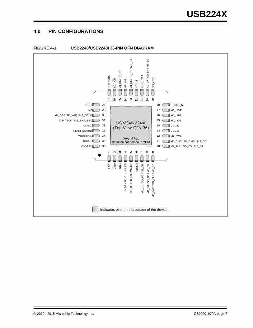
4.0 PIN CONFIGURATIONS
FIGURE 4-1: USB2240/USB2240I 36-PIN QFN DIAGRAM
Ground Pad(must be connected to VSS)
USB2240/2240I(Top View QFN-36)
Indicates pins on the bottom of the device.
26
xD_D
6 / S
D_D
3 / M
S_D
3
25
SD
_nC
D
24
xD_D
5 / S
D_D
2
23
MS
_IN
S
22
VD
D33
21
CR
D_P
WR
20
19
RX
D /
SD
A2
7
18
17
16
15
14
13
12
11
10
28
29
31
32
33
36
35
34
30
1 2 3 4 5 6 7 8 9
TEST
NC
xD_D4 / (SD_WP) / MS_SCLK
TXD / SCK / MS_SKT_SEL
XTAL2
XTAL1 (CLKIN)
VDD18PLL
RBIAS
VDDA33
LED
US
B+
US
B-
xD_D
3 /
SD
_D1
/ M
S_
D5
xD_D
2 /
SD
_D0
/ M
S_
D4
VD
D33
xD_D
0 /
SD
_D6
/ M
S_D
7
xD_n
WP
/ S
D_C
LK /
MS
_BS
xD_ALE / SD_D5 / MS_D1
VDD18
xD_nWE
xD_CLE / SD_CMD / MS_D0
xD_nCE
xD_nRE
xD_nB/R
RESET_N
(xD
_nC
D)
xD_
D7
/ S
D_D
4 /
MS
_D
2
xD_D
1 /
SD
_D7
/ M
S_D
6
VDD33
2010 - 2015 Microchip Technology Inc. DS00001979A-page 7

USB224X
FIGURE 4-2: USB2241/USB2241I 36-PIN QFN DIAGRAM
Ground Pad(must be connected to VSS)
USB2241/2241I(Top View QFN-36)
Indicates pins on the bottom of the device.
26
SD
_D3
/ MS
_D3
25
SD
_nC
D
24
SD
_D2
23
MS
_IN
S
22
VD
D33
21
CR
D_P
WR
20
19
RX
D /
SD
A2
7
18
17
16
15
14
13
12
11
10
28
29
31
32
33
36
35
34
30
1 2 3 4 5 6 7 8 9
TEST
NC
SD_WP / MS_SCLK
TXD / SCK / MS_SKT_SEL
XTAL2
XTAL1 (CLKIN)
VDD18PLL
RBIAS
VDDA33
LE
D
US
B+
US
B-
SD
_D1
/ M
S_D
5
SD
_D0
/ M
S_D
4
VD
D33
SD
_D6
/ M
S_D
7
SD
_CLK
/ M
S_B
S
SD_D5 / MS_D1
VDD18
NC
SD_CMD / MS_D0
NC
NC
NC
RESET_N
NC
SD
_D4
/ MS
_D2
SD
_D7
/ M
S_D
6
VDD33
DS00001979A-page 8 2010 - 2015 Microchip Technology Inc.

USB224X
FIGURE 4-3: USB2244/USB2244I 36-PIN QFN DIAGRAM
Ground Pad(must be connected to VSS)
USB2244/2244I(Top View QFN-36)
Indicates pins on the bottom of the device.
26
SD
_D
3
25
SD
_nC
D
24
SD
_D
2
23
NC
22V
DD
33
21C
RD
_PW
R
20 19
RX
D /
SD
A27
18
17
16
15
14
13
12
11
10
28
29
31
32
33
36
35
34
30
1 2 3 4 5 6 7 8 9
TEST
NC
SD_WP
TXD / SCK
XTAL2
XTAL1 (CLKIN)
VDD18PLL
RBIAS
VDDA33
LED
US
B+
US
B-
S
D_D
1
SD
_D
0
V
DD
33
S
D_D
6
SD
_CL
K
SD_D5
VDD18
NC
SD_CMD
NC
NC
NC
RESET_N
NC
SD
_D
4
S
D_D
7
VDD33
2010 - 2015 Microchip Technology Inc. DS00001979A-page 9
USB224X
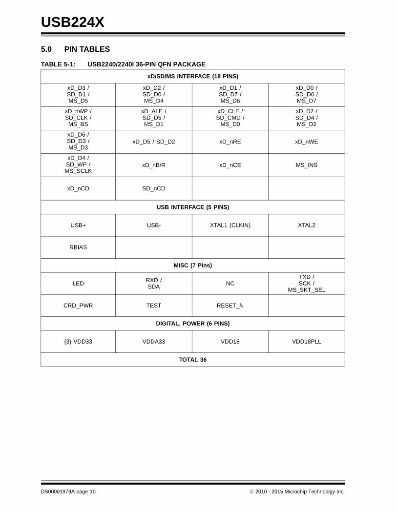
5.0 PIN TABLES
TABLE 5-1: USB2240/2240I 36-PIN QFN PACKAGE
xD/SD/MS INTERFACE (18 PINS)
xD_D3 / SD_D1 /MS_D5
xD_D2 / SD_D0 / MS_D4
xD_D1 / SD_D7 / MS_D6
xD_D0 / SD_D6 / MS_D7
xD_nWP / SD_CLK /
MS_BS
xD_ALE / SD_D5 / MS_D1
xD_CLE / SD_CMD /
MS_D0
xD_D7 / SD_D4 / MS_D2
xD_D6 / SD_D3 / MS_D3
xD_D5 / SD_D2 xD_nRE xD_nWE
xD_D4 / SD_WP / MS_SCLK
xD_nB/R xD_nCE MS_INS
xD_nCD SD_nCD
USB INTERFACE (5 PINS)
USB+ USB- XTAL1 (CLKIN) XTAL2
RBIAS
MISC (7 Pins)
LED RXD / SDA NC
TXD / SCK /
MS_SKT_SEL
CRD_PWR TEST RESET_N
DIGITAL, POWER (6 PINS)
(3) VDD33 VDDA33 VDD18 VDD18PLL
TOTAL 36
DS00001979A-page 10 2010 - 2015 Microchip Technology Inc.

USB224X
TABLE 5-2: USB2241/2241I 36-PIN QFN PACKAGE
SD/MS INTERFACE (14 PINS)
SD_D1 /MS_D5
SD_D0 / MS_D4
SD_D7 / MS_D6
SD_D6 / MS_D7
SD_CLK / MS_BS
SD_D5 / MS_D1
SD_CMD / MS_D0
SD_D4 / MS_D2
SD_D3 / MS_D3
SD_D2 SD_WP / MS_SCLK
MS_INS
NC SD_nCD
USB INTERFACE (5 PINS)
USB+ USB- XTAL1 (CLKIN) XTAL2
RBIAS
MISC (11 Pins)
LEDRXD / SDA NC
TXD / SCK /
MS_SKT_SEL
CRD_PWR TEST RESET_N (4) NC
DIGITAL, POWER (6 PINS)
(3) VDD33 VDDA33 VDD18 VDD18PLL
TOTAL 36
2010 - 2015 Microchip Technology Inc. DS00001979A-page 11
USB224X
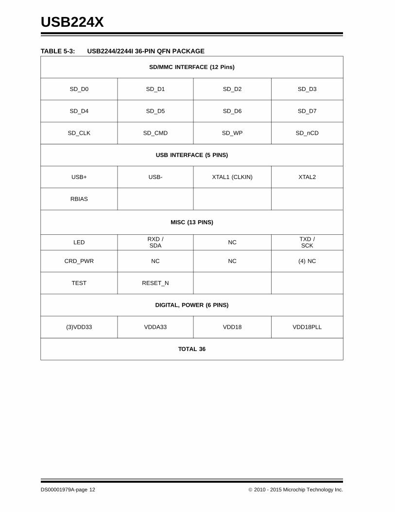
TABLE 5-3: USB2244/2244I 36-PIN QFN PACKAGE
SD/MMC INTERFACE (12 Pins)
SD_D0 SD_D1 SD_D2 SD_D3
SD_D4 SD_D5 SD_D6 SD_D7
SD_CLK SD_CMD SD_WP SD_nCD
USB INTERFACE (5 PINS)
USB+ USB- XTAL1 (CLKIN) XTAL2
RBIAS
MISC (13 PINS)
LED RXD / SDA NC TXD /
SCK
CRD_PWR NC NC (4) NC
TEST RESET_N
DIGITAL, POWER (6 PINS)
(3)VDD33 VDDA33 VDD18 VDD18PLL
TOTAL 36
DS00001979A-page 12 2010 - 2015 Microchip Technology Inc.

USB224X
6.0 PIN DESCRIPTIONS
This section provides a detailed description of each signal. The signals are arranged in functional groups according totheir associated interface. The pin descriptions are applied when using the internal default firmware and can be refer-enced in Section 7.0, "Pin Configurations," on page 18. Please reference Section 2.0, "Acronyms," on page 4 for a listof the acronyms used.
The “n” symbol in the signal name indicates that the active, or asserted, state occurs when the signal is at a low voltagelevel. When “n” is not present in the signal name, the signal is asserted at the high voltage level.
The terms assertion and negation are used exclusively. This is done to avoid confusion when working with a mixture of“active low” and “active high” signals. The term assert, or assertion, indicates that a signal is active, independent ofwhether that level is represented by a high or low voltage. The term negate, or negation, indicates that a signal is inac-tive.
6.1 USB224x 36-Pin QFN Pin Descriptions
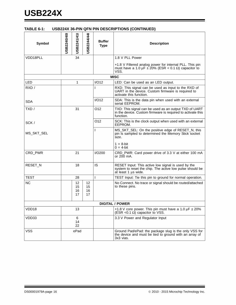
TABLE 6-1: USB224X 36-PIN QFN PIN DESCRIPTIONS
Symbol
US
B22
40/4
0I
US
B22
41/4
1I
US
B22
44/4
4I
Buffer Type
Description
xD-PICTURE CARD (xD) INTERFACE (APPLIES ONLY TO USB2240/USB2240I)
xD_D[7:0] 202325304578
I/O12PD xD Data
These bi-directional data signals have weak internal pull-down resistors.
xD_nWP 9 O12PD xD Write Protect
This pin is an active low write protect signal for the xD device and has a weak pull-down resistor that is permanently enabled.
xD_ALE 10 O12PD xD Address Strobe
This pin is an active high Address Latch Enable signal for the xD device and has a weak pull-down resistor that is permanently enabled.
xD_CLE 11 O12PD xD Command Strobe
This pin is an active high Command Latch Enable signal for the xD device and has a weak pull-down resistor that is permanently enabled.
xD_nRE 16 O12PU xD Read Enable
This pin is an active low read strobe signal for the xD device.
When using the internal FET, this pin has a weak internal pull-up resistor that is tied to the output of the internal power FET.
If an external FET is used (Internal FET is disabled), then the internal pull-up is not available (external pull-ups must be used).
2010 - 2015 Microchip Technology Inc. DS00001979A-page 13

USB224X
xD_nWE 12 O12PU xD Write Enable
This pin is an active low write strobe signal for the xD device.
When using the internal FET, this pin has a weak internal pull-up resistor that is tied to the output of the internal power FET.
If an external FET is used (Internal FET is disabled), then the internal pull-up is not available (external pull-ups must be used).
xD_nB/R 17 IPU xD Busy or Data Ready
This pin is connected to the BSY/RDY pin of the xD device.
When using the internal FET, this pin has a weak internal pull-up resistor that is tied to the output of the internal power FET.
If an external FET is used (Internal FET is disabled), then the internal pull-up is not available (external pull-ups must be used).
xD_nCD 19 I/O12 xD Card Detection
This is designated by the default firmware as the xD-Picture card detection pin.
Note: This pin can be left unconnected if the socket is not used.
xD_nCE 15 O12PU xD Chip Enable
This pin is the active low chip enable signal to the xD device.
When using the internal FET, this pin has a weak internal pull-up resistor that is tied to the output of the internal power FET.
If an external FET is used (Internal FET is disabled), then the internal pull-up is not available (external pull-ups must be used).
MEMORY STICK (MS) INTERFACE
MS_D[7:0] 8745
23201011
I/O12PD MS System Data In/Out
These pins are the bi-directional data signals for the MS device. MS_D0, MS_D2, and MS_D3 have weak pull-down resistors.
In serial mode, the most significant bit (MSB) of each byte is transmitted first by either MSC or MS device on MS_D0.
In parallel mode, MS_D1 has a pull-down resistor, otherwise it is disabled.
In 4- or 8-bit parallel mode, there is a weak pull-down resistor on all MS_D7 - 0 signals.
TABLE 6-1: USB224X 36-PIN QFN PIN DESCRIPTIONS (CONTINUED)
Symbol
US
B2
240
/40I
US
B2
241
/41I
US
B2
244
/44I
Buffer Type
Description
DS00001979A-page 14 2010 - 2015 Microchip Technology Inc.

USB224X
MS_BS 9 O12 MS Bus State
This pin is connected to the bus state (BS) pin of the MS device. It is used to control the bus states 0, 1, 2 and 3 (BS0, BS1, BS2 and BS3) of the MS device.
MS_SCLK 30 O12 MS System CLK
This pin is an output clock signal to the MS device.The clock frequency is software configurable.
MS_INS 24 IPU MS Card Insertion
This is designated by the default firmware as the Memory Stick card detection pin.
Note: This pin can be left unconnected if the socket is not used.
SECURE DIGITAL (SD) / MULTIMEDIACARD (MMC) INTERFACE
SD_D[7:0] 78
1020232545
78
1020232545
I/O12PU SD Data
The pins are bi-directional data signals SD_D0 - SD_D7 and have weak pull-up resistors.
SD_CLK 9 9 O12 SD Clock
This is an output clock signal to SD/MMC device. The clock frequency is software configurable.
SD_CMD 11 11 I/O12PU SD Command
This is a bi-directional signal that connects to the CMD signal of the SD/MMC device and has a weak internal pull-up resistor.
SD_WP SD Write Protect Detection
SD_nCD SD Card Detect
USB INTERFACE
USB+USB-
23
I/O-U USB Bus Data
These pins connect to the USB bus data signals.
RBIAS 35 I-R USB Transceiver Bias
A 12.0 kΩ, ± 1.0% resistor is attached from VSS to this pin in order to set the transceiver's internal bias currents.
XTAL1 (CLKIN) 33 ICLKx 24 MHz Crystal (External clock input)
This pin can be connected to one terminal of the crystal or can be connected to an external 24 MHz clock when a crystal is not used.
XTAL2 32 OCLKx 24 MHz Crystal
This is the other terminal of the crystal, or it is left open when an external clock source is used to drive XTAL1(CLKIN).
VDDA33 36 3.3 V Analog Power
TABLE 6-1: USB224X 36-PIN QFN PIN DESCRIPTIONS (CONTINUED)
Symbol
US
B2
240
/40I
US
B2
241
/41I
US
B2
244
/44I
Buffer Type
Description
2010 - 2015 Microchip Technology Inc. DS00001979A-page 15
USB224X
VDD18PLL 34 1.8 V PLL Power
+1.8 V Filtered analog power for internal PLL. This pin must have a 1.0 μF ± 20% (ESR < 0.1 Ω) capacitor to VSS.
MISC
LED 1 I/O12 LED: Can be used as an LED output.
RXD /
SDA
I RXD: This signal can be used as input to the RXD of UART in the device. Custom firmware is required to activate this function.
I/O12 SDA: This is the data pin when used with an external serial EEPROM.
TXD /
SCK /
MS_SKT_SEL
31 O12 TXD: This signal can be used as an output TXD of UART in the device. Custom firmware is required to activate this function.
O12 SCK: This is the clock output when used with an external EEPROM.
I MS_SKT_SEL: On the positive edge of RESET_N, this pin is sampled to determined the Memory Stick socket size.
1 = 8-bit0 = 4-bit
CRD_PWR 21 I/O200 CRD_PWR: Card power drive of 3.3 V at either 100 mA or 200 mA.
RESET_N 18 IS RESET Input: This active low signal is used by the system to reset the chip. The active low pulse should be at least 1 μs wide.
TEST 28 I TEST Input: Tie this pin to ground for normal operation.
NC 12151617
12151617
No Connect. No trace or signal should be routed/attached to these pins.
DIGITAL / POWER
VDD18 13 +1.8 V core power. This pin must have a 1.0 μF ± 20% (ESR <0.1 Ω) capacitor to VSS.
VDD33 61422
3.3 V Power and Regulator Input
VSS ePad Ground Pad/ePad: the package slug is the only VSS for the device and must be tied to ground with an array of 3x3 vias.
TABLE 6-1: USB224X 36-PIN QFN PIN DESCRIPTIONS (CONTINUED)
Symbol
US
B2
240
/40I
US
B2
241
/41I
US
B2
244
/44I
Buffer Type
Description
DS00001979A-page 16 2010 - 2015 Microchip Technology Inc.

USB224X
6.2 Buffer Type Descriptions
TABLE 6-2: BUFFER TYPE DESCRIPTIONS
Buffer Description
I Input
IPU Input with internal weak pull-up resistor
IS Input with Schmitt trigger
I/O12 Input/output buffer with 12 mA sink and 12 mA source
I/O200 Input/Output buffer 12 mA with FET disabled, 100/200 mA source only when the FET is enabled
I/O12PD Input/output buffer with 12 mA sink and 12 mA source with an internal weak pull-down resistor
I/O12PU Input/output buffer with 12 mA sink and 12 mA source with a pull-up resistor
O12 Output buffer with 12 mA source
O12PU Output buffer with 12 mA sink and 12 mA source, with a pull-up resistor
O12PD Output buffer with 12 mA sink and 12 mA source, with a pull-down resistor
ICLKx XTAL clock input
OCLKx XTAL clock output
I/O-U Analog input/output as defined in the USB 2.0 Specification
I-R RBIAS
Note: The DC characteristics are outlined in Section 9.3, on page 32.
2010 - 2015 Microchip Technology Inc. DS00001979A-page 17
USB224X
7.0 PIN CONFIGURATIONS
7.1 Card Reader
The Microchip USB224x is fully compliant with the following flash media card reader specifications:
• Secure Digital 2.0
- HS-SD and SDHC
- TransFlash™ and reduced form factor media
• MultiMediaCard 4.2
- 1/4/8 bit MMC
• Memory Stick 1.43
• Memory Stick Pro Format 1.02
• Memory Stick Pro-HG Duo Format 1.01
- Memory Stick, MS Duo, HS-MS, MS Pro-HG, MS Pro
• Memory Stick Duo 1.10
• xD-Picture Card 1.2
7.2 System Configurations
7.2.1 EEPROM
The USB224x can be configured via a 2-wire (I2C) EEPROM (512x8) flash device containing the options for theUSB224x. If an external configuration device does not exist the internal default values will be used. If one of the externaldevices is used for configuration, the OEM can update the values through the USB interface. The device will then“attach” to the upstream USB host.
The USBDM tool set is available in the USB224x/USB225x Card Reader software release package. To download thesoftware package from Microchip's website, please visit:
http://www.microchip.com/SWLibraryWeb/product.aspx?product=OBJ Card Reader
to go to the OBJ Card Reader Software Download Agreement. Review the license, and if you agree, check the "I agree"box and then select “Confirm”. You will then be able to download the USB224x/USB225x Card reader combo releasepackage zip file containing the USBDM tool set. Please note that the following applies to the system values and descrip-tions when used:
• N/A = Not applicable to this part
• Reserved = For internal use
7.2.2 EEPROM DATA DESCRIPTOR
TABLE 7-1: INTERNAL FLASH MEDIA CONTROLLER CONFIGURATIONS
Address Register Name Description Internal Default Value
00h USB_SER_LEN USB Serial String Descriptor Length
1Ah
01h USB_SER_TYP USB Serial String Descriptor Type
03h
02h-19h USB_SER_NUM USB Serial Number "000000225001" (See Note 7-1)
1Ah-1Bh USB_VID USB Vendor Identifier 0424
1Ch-1Dh USB_PID USB Product Identifier 2240
1Eh USB_LANG_LEN USB Language String Descriptor Length
04h
1Fh USB_LANG_TYP USB Language String Descriptor Type
03h
20h USB_LANG_ID_LSB USB Language Identifier Least Significant Byte
09h(See Note 7-2)
DS00001979A-page 18 2010 - 2015 Microchip Technology Inc.
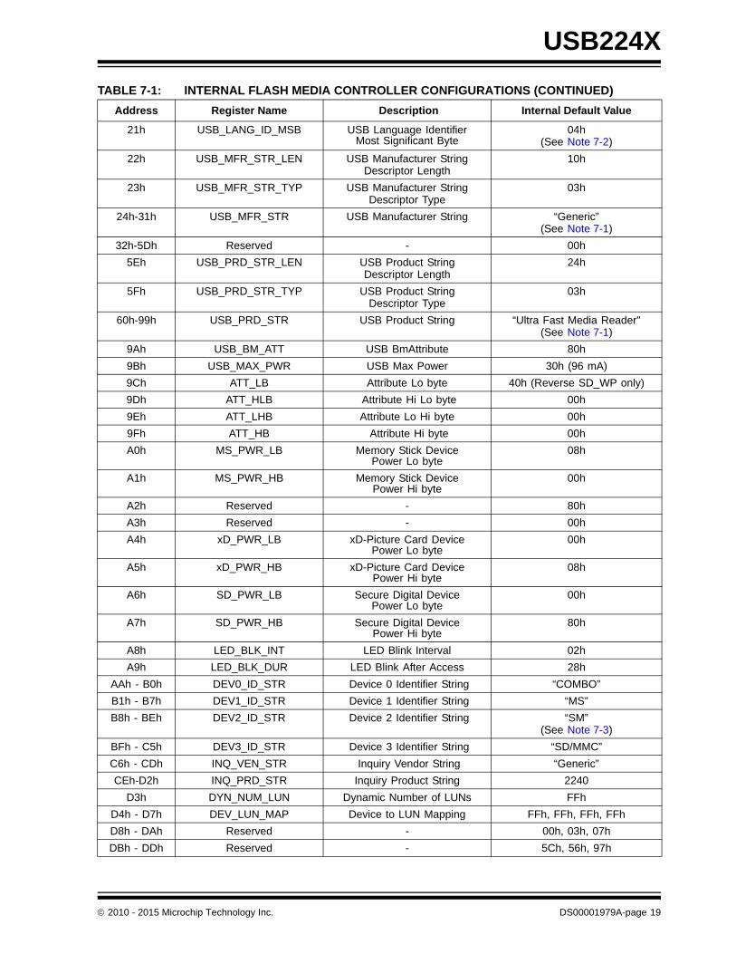
USB224X
21h USB_LANG_ID_MSB USB Language Identifier Most Significant Byte
04h(See Note 7-2)
22h USB_MFR_STR_LEN USB Manufacturer String Descriptor Length
10h
23h USB_MFR_STR_TYP USB Manufacturer String Descriptor Type
03h
24h-31h USB_MFR_STR USB Manufacturer String “Generic”(See Note 7-1)
32h-5Dh Reserved - 00h
5Eh USB_PRD_STR_LEN USB Product StringDescriptor Length
24h
5Fh USB_PRD_STR_TYP USB Product StringDescriptor Type
03h
60h-99h USB_PRD_STR USB Product String “Ultra Fast Media Reader"(See Note 7-1)
9Ah USB_BM_ATT USB BmAttribute 80h
9Bh USB_MAX_PWR USB Max Power 30h (96 mA)
9Ch ATT_LB Attribute Lo byte 40h (Reverse SD_WP only)
9Dh ATT_HLB Attribute Hi Lo byte 00h
9Eh ATT_LHB Attribute Lo Hi byte 00h
9Fh ATT_HB Attribute Hi byte 00h
A0h MS_PWR_LB Memory Stick DevicePower Lo byte
08h
A1h MS_PWR_HB Memory Stick DevicePower Hi byte
00h
A2h Reserved - 80h
A3h Reserved - 00h
A4h xD_PWR_LB xD-Picture Card DevicePower Lo byte
00h
A5h xD_PWR_HB xD-Picture Card DevicePower Hi byte
08h
A6h SD_PWR_LB Secure Digital DevicePower Lo byte
00h
A7h SD_PWR_HB Secure Digital DevicePower Hi byte
80h
A8h LED_BLK_INT LED Blink Interval 02h
A9h LED_BLK_DUR LED Blink After Access 28h
AAh - B0h DEV0_ID_STR Device 0 Identifier String “COMBO”
B1h - B7h DEV1_ID_STR Device 1 Identifier String “MS”
B8h - BEh DEV2_ID_STR Device 2 Identifier String “SM” (See Note 7-3)
BFh - C5h DEV3_ID_STR Device 3 Identifier String “SD/MMC”
C6h - CDh INQ_VEN_STR Inquiry Vendor String “Generic”
CEh-D2h INQ_PRD_STR Inquiry Product String 2240
D3h DYN_NUM_LUN Dynamic Number of LUNs FFh
D4h - D7h DEV_LUN_MAP Device to LUN Mapping FFh, FFh, FFh, FFh
D8h - DAh Reserved - 00h, 03h, 07h
DBh - DDh Reserved - 5Ch, 56h, 97h
TABLE 7-1: INTERNAL FLASH MEDIA CONTROLLER CONFIGURATIONS (CONTINUED)
Address Register Name Description Internal Default Value
2010 - 2015 Microchip Technology Inc. DS00001979A-page 19

USB224X
Note 7-1 This value is a UNICODE UTF-16LE encoded string value that meets the USB 2.0 specification(Revision 2.0, 2000). Values in double quotations without this note are ASCII values.
Note 7-2 For a list of the most current 16-bit language ID’s defined by the USB-IF, please visithttp://www.unicode.org or consult The Unicode Standard, Worldwide Character Encoding, (Version4.0), The Unicode Consortium, Addison-Wesley Publishing Company, Reading, Massachusetts.
Note 7-3 The “SM” value will be overridden with “xD” once an xD-Picture Card has been identified.
7.2.3 EEPROM DATA DESCRIPTOR REGISTER DESCRIPTIONS
7.2.3.1 00h: USB Serial String Descriptor Length
7.2.3.2 01h: USB Serial String Descriptor Type
7.2.3.3 02h-19h: USB Serial Number Option
7.2.3.4 1Ah-1Bh: USB Vendor ID Option
7.2.3.5 1Ch-1Dh: USB Product ID Option
7.2.3.6 1Eh: USB Language Identifier Descriptor Length
DEh-FBh Not Applicable - 00h
FCh-FFh NVSTORE_SIG Non-Volatile Storage Signature “ATA2”
Byte Name Description
0 USB_SER_LEN USB serial string descriptor length as defined by Section 9.6.7 “String” of the USB 2.0 Specification (Revision 2.0, 2000). This field is the “bLength” which describes the size of the string descriptor (in bytes).
Byte Name Description
1 USB_SER_TYP USB serial string descriptor type as defined by Section 9.6.7 “String” of the USB 2.0 Specification (Revision 2.0, 2000). This field is the “bDescriptorType” which is a constant value associated with a string descriptor type.
Byte Name Description
25:2 USB_SER_NUM Maximum string length is 12 hex digits. Must be unique to each device.
Byte Name Description
1:0 USB_VID This ID is unique for every vendor. The vendor ID is assigned by the USB Implementer’s Forum.
Byte Name Description
1:0 USB_PID This ID is unique for every product. The product ID is assigned by the vendor.
Byte Name Description
0 USB_LANG_LEN USB language ID string descriptor length as defined by Section 9.6.7 “String” of the USB 2.0 Specification (Revision 2.0, 2000). This field is the “bLength” which describes the size of the string descriptor (in bytes).
TABLE 7-1: INTERNAL FLASH MEDIA CONTROLLER CONFIGURATIONS (CONTINUED)
Address Register Name Description Internal Default Value
DS00001979A-page 20 2010 - 2015 Microchip Technology Inc.

USB224X
7.2.3.7 1Fh: USB Language Identifier Descriptor Type
7.2.3.8 20h: USB Language Identifier Least Significant Byte
7.2.3.9 21h: USB Language Identifier Most Significant Byte
7.2.3.10 22h: USB Manufacturer String Descriptor Length
7.2.3.11 23h: USB Manufacturer String Descriptor Type
7.2.3.12 24h-31h: USB Manufacturer String Option
7.2.3.13 32h-5Dh: Reserved
7.2.3.14 5Eh: USB Product String Descriptor Length
Byte Name Description
1 USB_LANG_TYP USB language ID string descriptor type as defined by Section 9.6.7 “String” of the USB 2.0 Specification (Revision 2.0, 2000). This field is the “bDescriptorType” which is a constant value associated with a string descriptor type.
Byte Name Description
2 USB_LANG_ID_LSB
English language code = ‘0409’. See Note 7-2 to reference additional language ID’s defined by the USB-IF.
Byte Name Description
3 USB_LANG_ID_MSB
English language code = ‘0409’. See Note 7-2 to reference additional language ID’s defined by the USB-IF.
Byte Name Description
0 USB_MFR_STR_LEN
USB manufacturer string descriptor length as defined by Section 9.6.7 “String” of the USB 2.0 Specification (Revision 2.0, 2000). This field is the “bLength” which describes the size of the string descriptor (in bytes).
Byte Name Description
1 USB_MFR_STR_TYP
USB manufacturer string descriptor type as defined by Section 9.6.7 “String” of the USB 2.0 Specification (Revision 2.0, 2000). This field is the “bDescriptorType” which is a constant value associated with a string descriptor type.
Byte Name Description
15:2 USB_MFR_STR The maximum string length is 29 characters.
Byte Name Description
59:16 Reserved Reserved.
Byte Name Description
0 USB_PRD_STR_LEN
USB product string descriptor length as defined by Section 9.6.7 “String” of the USB 2.0 Specification (Revision 2.0, 2000). This field is the “bLength” which describes the size of the string descriptor (in bytes). Maximum string length is 29 characters
2010 - 2015 Microchip Technology Inc. DS00001979A-page 21
USB224X
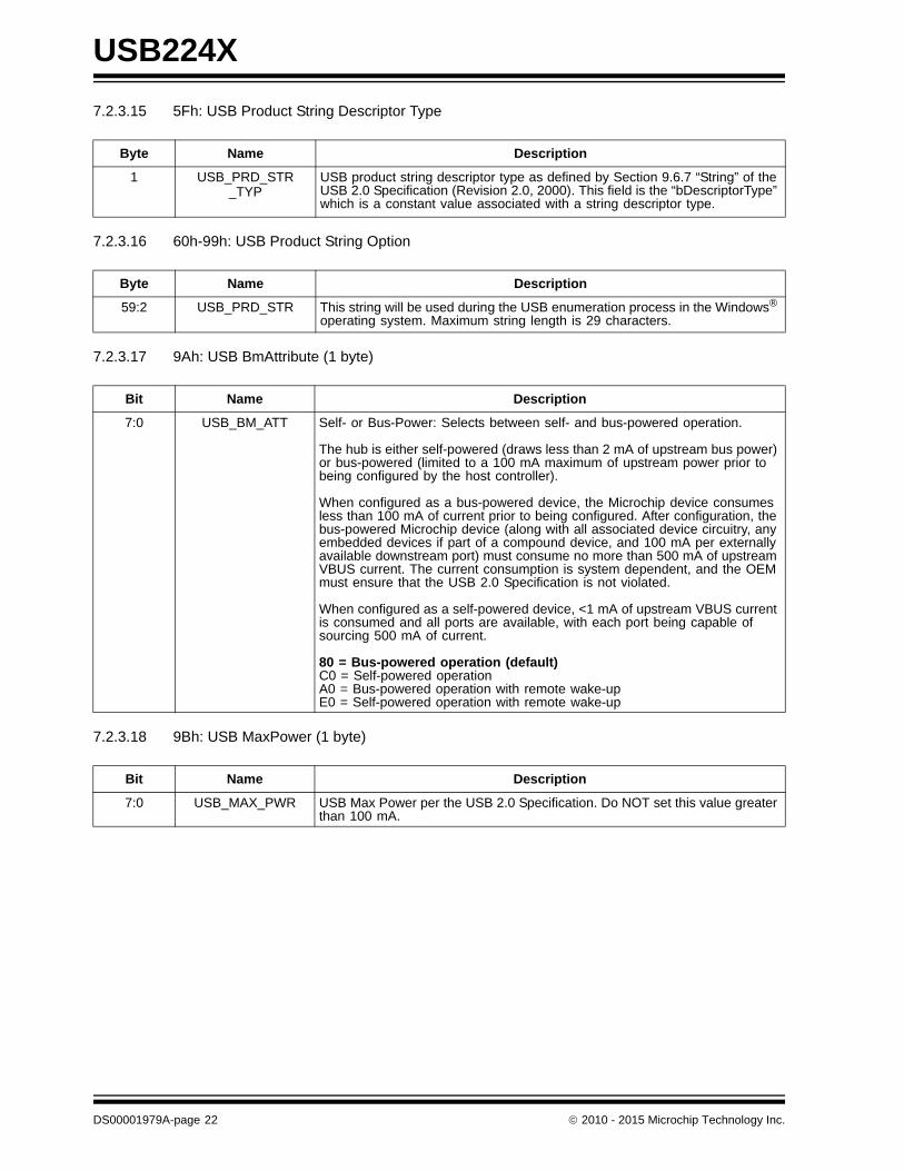
7.2.3.15 5Fh: USB Product String Descriptor Type
7.2.3.16 60h-99h: USB Product String Option
7.2.3.17 9Ah: USB BmAttribute (1 byte)
7.2.3.18 9Bh: USB MaxPower (1 byte)
Byte Name Description
1 USB_PRD_STR_TYP
USB product string descriptor type as defined by Section 9.6.7 “String” of the USB 2.0 Specification (Revision 2.0, 2000). This field is the “bDescriptorType” which is a constant value associated with a string descriptor type.
Byte Name Description
59:2 USB_PRD_STR This string will be used during the USB enumeration process in the Windows® operating system. Maximum string length is 29 characters.
Bit Name Description
7:0 USB_BM_ATT Self- or Bus-Power: Selects between self- and bus-powered operation.
The hub is either self-powered (draws less than 2 mA of upstream bus power) or bus-powered (limited to a 100 mA maximum of upstream power prior to being configured by the host controller).
When configured as a bus-powered device, the Microchip device consumes less than 100 mA of current prior to being configured. After configuration, the bus-powered Microchip device (along with all associated device circuitry, any embedded devices if part of a compound device, and 100 mA per externally available downstream port) must consume no more than 500 mA of upstream VBUS current. The current consumption is system dependent, and the OEM must ensure that the USB 2.0 Specification is not violated.
When configured as a self-powered device, <1 mA of upstream VBUS current is consumed and all ports are available, with each port being capable of sourcing 500 mA of current.
80 = Bus-powered operation (default)C0 = Self-powered operationA0 = Bus-powered operation with remote wake-upE0 = Self-powered operation with remote wake-up
Bit Name Description
7:0 USB_MAX_PWR USB Max Power per the USB 2.0 Specification. Do NOT set this value greater than 100 mA.
DS00001979A-page 22 2010 - 2015 Microchip Technology Inc.

USB224X
7.2.3.19 9Ch-9Fh: Attribute Byte Descriptions
7.2.4 A0H-A7H: DEVICE POWER CONFIGURATION
The USB224x has one internal FET which can be utilized for card power. This section describes the default internalconfiguration. The settings are stored in NVSTORE and provide the following features:
1. A card can be powered by an external FET or by an internal FET.
2. The power limit can be set to 100 mA or 200 mA (Default) for the internal FET.
Each media uses two bytes to store its device power configuration. Bit 3 selects between internal or external card powerFET options. For internal FET card power control, bits 0 through 2 are used to set the power limit. The “Device PowerConfiguration” bits are ignored unless the “Enable Device Power Configuration” bit is set. See Section 7.2.3.19, "9Ch-9Fh: Attribute Byte Descriptions," on page 23.
Byte Byte Name Bit Description
0 ATT_LB 3:0 Always reads ‘0’.
4 Inquire Manufacturer and Product ID Strings
‘1’ - Use the Inquiry Manufacturer and Product ID Strings.
‘0’ (default) - Use the USB Descriptor Manufacturer and Product ID Strings.
5 Always reads ‘0’.
6 Reverse SD Card Write Protect Sense
‘1’ (default) - SD cards will be write protected when SW_nWP is high, and writable when SW_nWP is low.
‘0’ - SD cards will be write protected when SW_nWP is low, and writable when SW_nWP is high.
7 Reserved.
1 ATT_HLB 3:0 Always reads ‘0’.
4 Activity LED True Polarity
‘1’ - Activity LED to Low True.
‘0’ (default) - Activity LED polarity to High True.
5 Common Media Insert / Media Activity LED
‘1’ - The activity LED will function as a common media inserted/media access LED.
‘0’ (default) - The activity LED will remain in its idle state until media is accessed.
6 Always reads ‘0’.
7 Reserved.
2 ATT_LHB 0 Attach on Card Insert / Detach on Card Removal
‘1’ - Attach on Insert is enabled.
‘0’ (default) - Attach on Insert is disabled.
1 Always reads ‘0’.
2 Enable Device Power Configuration
‘1’ - Custom Device Power Configuration stored in the NVSTORE is used.
‘0’ (default) - Default Device Power Configuration is used.
7:3 Always reads ‘0’.
3 ATT_HB 6:0 Always reads ‘0’.
7 xD Player Mode
2010 - 2015 Microchip Technology Inc. DS00001979A-page 23
USB224X
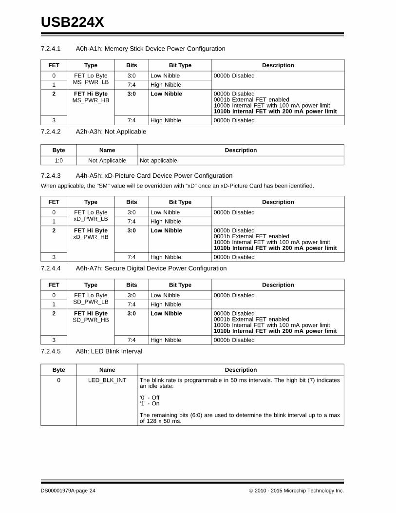
7.2.4.1 A0h-A1h: Memory Stick Device Power Configuration
7.2.4.2 A2h-A3h: Not Applicable
7.2.4.3 A4h-A5h: xD-Picture Card Device Power Configuration
When applicable, the "SM" value will be overridden with “xD” once an xD-Picture Card has been identified.
7.2.4.4 A6h-A7h: Secure Digital Device Power Configuration
7.2.4.5 A8h: LED Blink Interval
FET Type Bits Bit Type Description
0 FET Lo ByteMS_PWR_LB
3:0 Low Nibble 0000b Disabled
1 7:4 High Nibble
2 FET Hi ByteMS_PWR_HB
3:0 Low Nibble 0000b Disabled0001b External FET enabled1000b Internal FET with 100 mA power limit1010b Internal FET with 200 mA power limit
3 7:4 High Nibble 0000b Disabled
Byte Name Description
1:0 Not Applicable Not applicable.
FET Type Bits Bit Type Description
0 FET Lo BytexD_PWR_LB
3:0 Low Nibble 0000b Disabled
1 7:4 High Nibble
2 FET Hi BytexD_PWR_HB
3:0 Low Nibble 0000b Disabled0001b External FET enabled1000b Internal FET with 100 mA power limit1010b Internal FET with 200 mA power limit
3 7:4 High Nibble 0000b Disabled
FET Type Bits Bit Type Description
0 FET Lo ByteSD_PWR_LB
3:0 Low Nibble 0000b Disabled
1 7:4 High Nibble
2 FET Hi ByteSD_PWR_HB
3:0 Low Nibble 0000b Disabled0001b External FET enabled1000b Internal FET with 100 mA power limit1010b Internal FET with 200 mA power limit
3 7:4 High Nibble 0000b Disabled
Byte Name Description
0 LED_BLK_INT The blink rate is programmable in 50 ms intervals. The high bit (7) indicates an idle state:
‘0’ - Off‘1’ - On
The remaining bits (6:0) are used to determine the blink interval up to a max of 128 x 50 ms.
DS00001979A-page 24 2010 - 2015 Microchip Technology Inc.
USB224X
7.2.4.6 A9h: LED Blink Duration
7.2.5 DEVICE ID STRINGS
These bytes are used to specify the LUN descriptor returned by the device. These bytes are used in combination withthe device to LUN mapping bytes in applications where the OEM wishes to reorder and rename the LUNs. If multipledevices are mapped to the same LUN (a COMBO LUN), then the CLUN#_ID_STR will be used to name the COMBOLUN instead of the individual device strings. When applicable, the "SM" value will be overridden with xD once an xD-Picture Card has been identified.
7.2.5.1 AAh-B0h: Device 0 Identifier String
7.2.5.2 B1h-B7h: Device 1 Identifier String
7.2.5.3 B8h-BEh: Device 2 Identifier String
7.2.5.4 BFh-C5h: Device 3 Identifier String
7.2.5.5 C6h-CDh: Inquiry Vendor String
7.2.5.6 CEh-D2h: Inquiry Product String
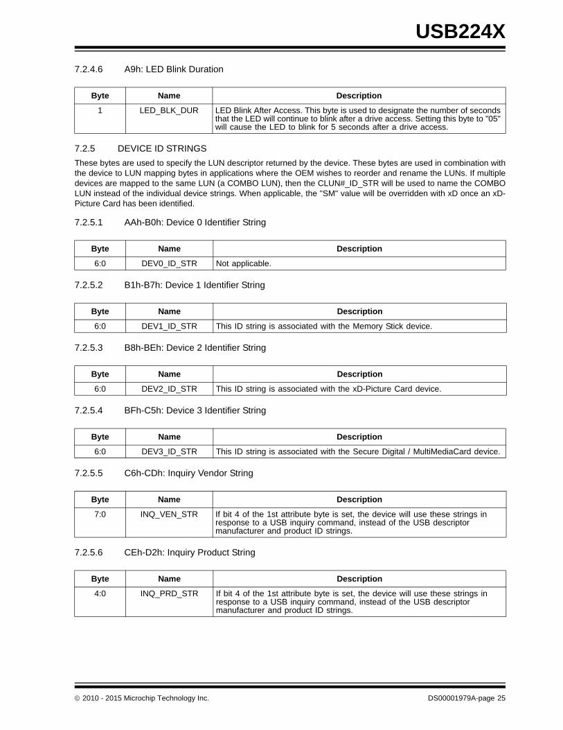
Byte Name Description
1 LED_BLK_DUR LED Blink After Access. This byte is used to designate the number of seconds that the LED will continue to blink after a drive access. Setting this byte to "05" will cause the LED to blink for 5 seconds after a drive access.
Byte Name Description
6:0 DEV0_ID_STR Not applicable.
Byte Name Description
6:0 DEV1_ID_STR This ID string is associated with the Memory Stick device.
Byte Name Description
6:0 DEV2_ID_STR This ID string is associated with the xD-Picture Card device.
Byte Name Description
6:0 DEV3_ID_STR This ID string is associated with the Secure Digital / MultiMediaCard device.
Byte Name Description
7:0 INQ_VEN_STR If bit 4 of the 1st attribute byte is set, the device will use these strings in response to a USB inquiry command, instead of the USB descriptor manufacturer and product ID strings.
Byte Name Description
4:0 INQ_PRD_STR If bit 4 of the 1st attribute byte is set, the device will use these strings in response to a USB inquiry command, instead of the USB descriptor manufacturer and product ID strings.
2010 - 2015 Microchip Technology Inc. DS00001979A-page 25

USB224X
7.2.5.7 D3h: Dynamic Number of LUNs
7.2.5.8 D4h-D7h: Device to LUN Mapping
7.2.5.9 D8h-FBh: Not Applicable
7.2.5.10 FCh-FFh: Non-Volatile Storage Signature
7.3 Default Configuration Option
The Microchip device can be configured via its internal default configuration. Please see Section 7.2.2, "EEPROM DataDescriptor" for specific details on how to enable default configuration. Please refer to Table 7-1 for the internal defaultvalues that are loaded when this option is selected.
7.3.1 EXTERNAL HARDWARE RESET_N
A valid hardware reset is defined as assertion of RESET_N for a minimum of 1 μs after all power supplies are withinoperating range. While reset is asserted, the device (and its associated external circuitry) consumes less than 500 μAof current from the upstream USB power source.
Assertion of RESET_N (external pin) causes the following:
1. The PHY is disabled and the differential pair will be in a high-impedance state.
2. All transactions immediately terminate; no states are saved.
3. All internal registers return to the default state.
4. The external crystal oscillator is halted.
5. The PLL is halted.
6. The processor is reset.
7. All media interfaces are reset.
Bit Name Description
7:0 DYN_NUM_LUN These bytes are used to specify the number of LUNs the device exposes to the host. These bytes are also used for icon sharing by assigning more than one LUN to a single icon. This is used in applications where the device utilizes a combo socket and the OEM wishes to have only a single icon displayed for one or more interfaces.
If this field is set to "FF", the program assumes that you are using the default value and icons will be configured per the default configuration.
Byte Name Description
3:0 DEV_LUN_MAP These registers map a device controller (SD/MMC, SM, and MS) to a Logical Unit Number (LUN). The device reports the mapped LUNs to the USB host in the USB descriptor during enumeration. The icon installer associates custom icons with the LUNs specified in these fields.
Setting a register to "FF" indicates that the device is not mapped. Setting all of the DEV_LUN_MAP registers for all devices to "FF" forces the use of the default mapping configuration. Not all configurations are valid. Valid configurations depend on the hardware, packaging, and OEM board layout. The number of unique LUNs mapped must match the value in the Section 7.2.5.7, "D3h: Dynamic Number of LUNs," on page 26.
Byte Name Description
35:0 Not Applicable Not Applicable.
Byte Name Description
3:0 NVSTORE_SIG This signature is used to verify the validity of the data in the first 256 bytes of the configuration area. The signature must be set to ‘ATA2’ for USB224x.
DS00001979A-page 26 2010 - 2015 Microchip Technology Inc.

USB224X
7.3.1.1 RESET_N for EEPROM Configuration
7.3.2 USB BUS RESET
In response to the upstream port signaling a reset to the device, the device does the following:
1. Sets default address to ‘0’.
2. Sets configuration to: Unconfigured.
3. All transactions are stopped.
4. Processor reinitializes and restarts.
5. All media interfaces are disabled.
FIGURE 7-1: RESET_N TIMING FOR EEPROM MODE
TABLE 7-2: RESET_N TIMING FOR EEPROM MODE
Name Description MIN TYP MAX Units
t1 RESET_N asserted 1 μsec
t2 Device recovery/stabilization 500 μsec
t3 8051 programs device configuration 20 50 msec
t4 USB attach 100 msec
t5 Host acknowledges attach and signals USB reset 100 msec
t6 USB idle Undefined msec
t7 Ready to handle requests (with or without data) 5 msec
Note: All power supplies must have reached the operating levels mandated in Section 9.0, "DC Parameters," onpage 31, prior to (or coincident with) the assertion of RESET_N.
t1 t2
t4t5 t6 t7
RESET_N
VSS
Hardware reset
asserted
Device Recovery/
Stabilization
8051 Sets Configuration
Registers
Attach USB
Upstream
USB Reset recovery
Idle
Start completion
request response
t3
2010 - 2015 Microchip Technology Inc. DS00001979A-page 27
USB224X
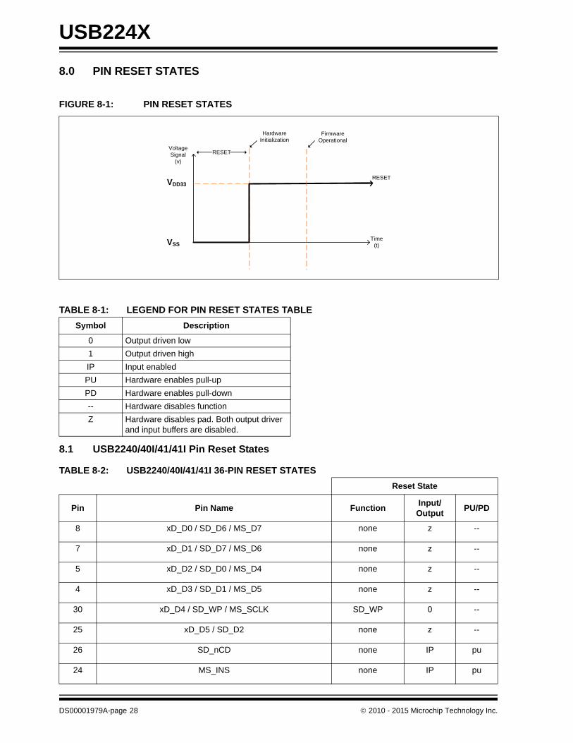
8.0 PIN RESET STATES
8.1 USB2240/40I/41/41I Pin Reset States
FIGURE 8-1: PIN RESET STATES
TABLE 8-1: LEGEND FOR PIN RESET STATES TABLE
Symbol Description
0 Output driven low
1 Output driven high
IP Input enabled
PU Hardware enables pull-up
PD Hardware enables pull-down
-- Hardware disables function
Z Hardware disables pad. Both output driver and input buffers are disabled.
TABLE 8-2: USB2240/40I/41/41I 36-PIN RESET STATES
Reset State
Pin Pin Name FunctionInput/Output
PU/PD
8 xD_D0 / SD_D6 / MS_D7 none z --
7 xD_D1 / SD_D7 / MS_D6 none z --
5 xD_D2 / SD_D0 / MS_D4 none z --
4 xD_D3 / SD_D1 / MS_D5 none z --
30 xD_D4 / SD_WP / MS_SCLK SD_WP 0 --
25 xD_D5 / SD_D2 none z --
26 SD_nCD none IP pu
24 MS_INS none IP pu
Voltage Signal
(v)
Time (t)
RESET
RESET
Hardware Initialization
FirmwareOperational
VDD33
VSS
DS00001979A-page 28 2010 - 2015 Microchip Technology Inc.
USB224X
23 xD_D6 / SD_D3 / MS_D3 none z --
20 xD_D7 / SD_D4 / MS_D2 none z --
9 xD_nWP / SD_CLK / MS_BS none z --
10 xD_ALE / SD_D5 / MS_D1 none z --
11 xD_CLE / SD_CMD / MS_D0 none z --
19 xD_nCD none IP pu
1 LED none 0 --
16 xD_nRE none z --
27 RXD / SDA none 0 --
29 none 0 --
31 TXD / SCK / MS_SKT_SEL none 0 --
21 CRD_PWR none z --
28 TEST TEST IP --
18 RESET_N RESET_N IP --
12 xD_nWE none z --
17 xD_nB/R none z --
15 xD_nCE none z --
2 USB+ USB+ z --
3 USB- USB- z --
Note: xD signals only apply to USB2240/USB2240I.
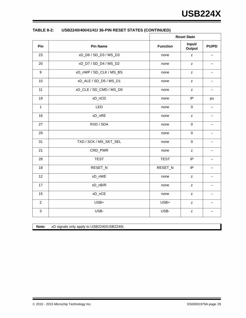
TABLE 8-2: USB2240/40I/41/41I 36-PIN RESET STATES (CONTINUED)
Reset State
Pin Pin Name FunctionInput/Output
PU/PD
2010 - 2015 Microchip Technology Inc. DS00001979A-page 29
USB224X
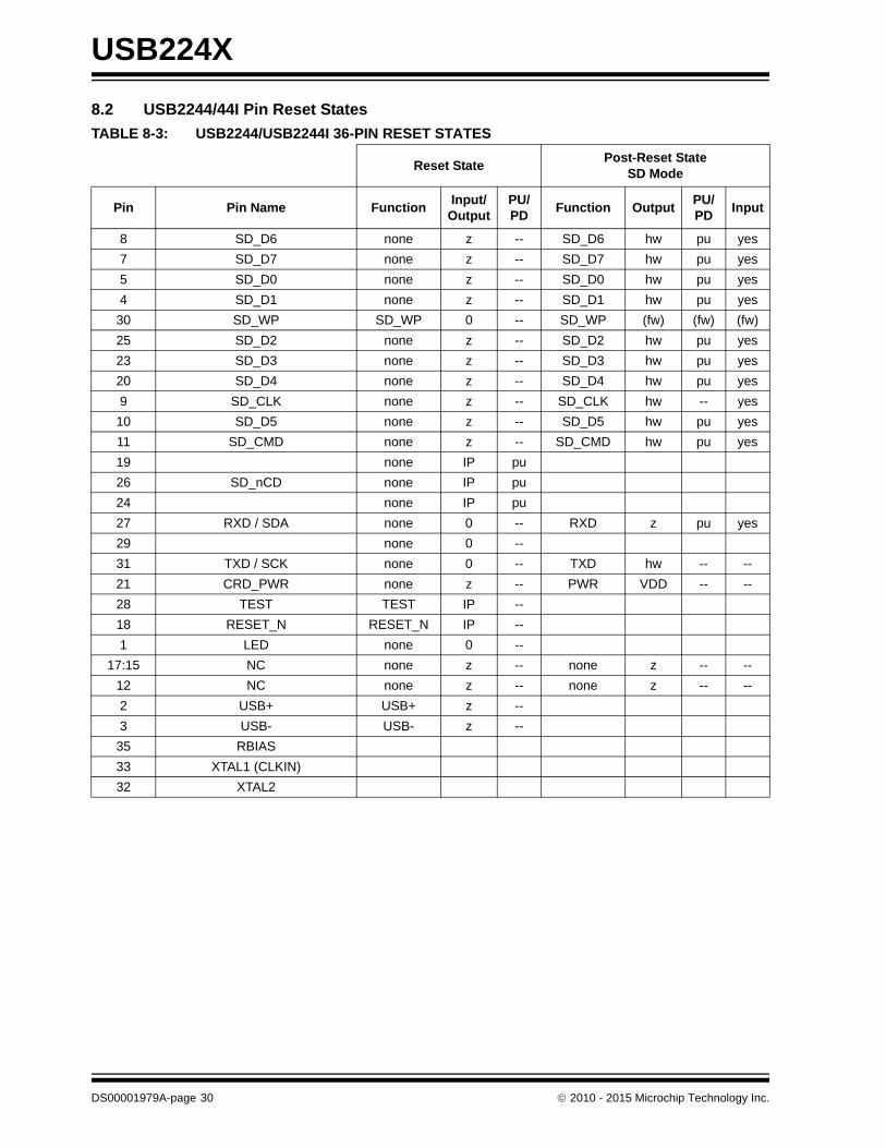
8.2 USB2244/44I Pin Reset States
TABLE 8-3: USB2244/USB2244I 36-PIN RESET STATES
Reset StatePost-Reset State
SD Mode
Pin Pin Name FunctionInput/
OutputPU/PD
Function OutputPU/PD
Input
8 SD_D6 none z -- SD_D6 hw pu yes
7 SD_D7 none z -- SD_D7 hw pu yes
5 SD_D0 none z -- SD_D0 hw pu yes
4 SD_D1 none z -- SD_D1 hw pu yes
30 SD_WP SD_WP 0 -- SD_WP (fw) (fw) (fw)
25 SD_D2 none z -- SD_D2 hw pu yes
23 SD_D3 none z -- SD_D3 hw pu yes
20 SD_D4 none z -- SD_D4 hw pu yes
9 SD_CLK none z -- SD_CLK hw -- yes
10 SD_D5 none z -- SD_D5 hw pu yes
11 SD_CMD none z -- SD_CMD hw pu yes
19 none IP pu
26 SD_nCD none IP pu
24 none IP pu
27 RXD / SDA none 0 -- RXD z pu yes
29 none 0 --
31 TXD / SCK none 0 -- TXD hw -- --
21 CRD_PWR none z -- PWR VDD -- --
28 TEST TEST IP --
18 RESET_N RESET_N IP --
1 LED none 0 --
17:15 NC none z -- none z -- --
12 NC none z -- none z -- --
2 USB+ USB+ z --
3 USB- USB- z --
35 RBIAS
33 XTAL1 (CLKIN)
32 XTAL2
DS00001979A-page 30 2010 - 2015 Microchip Technology Inc.
USB224X
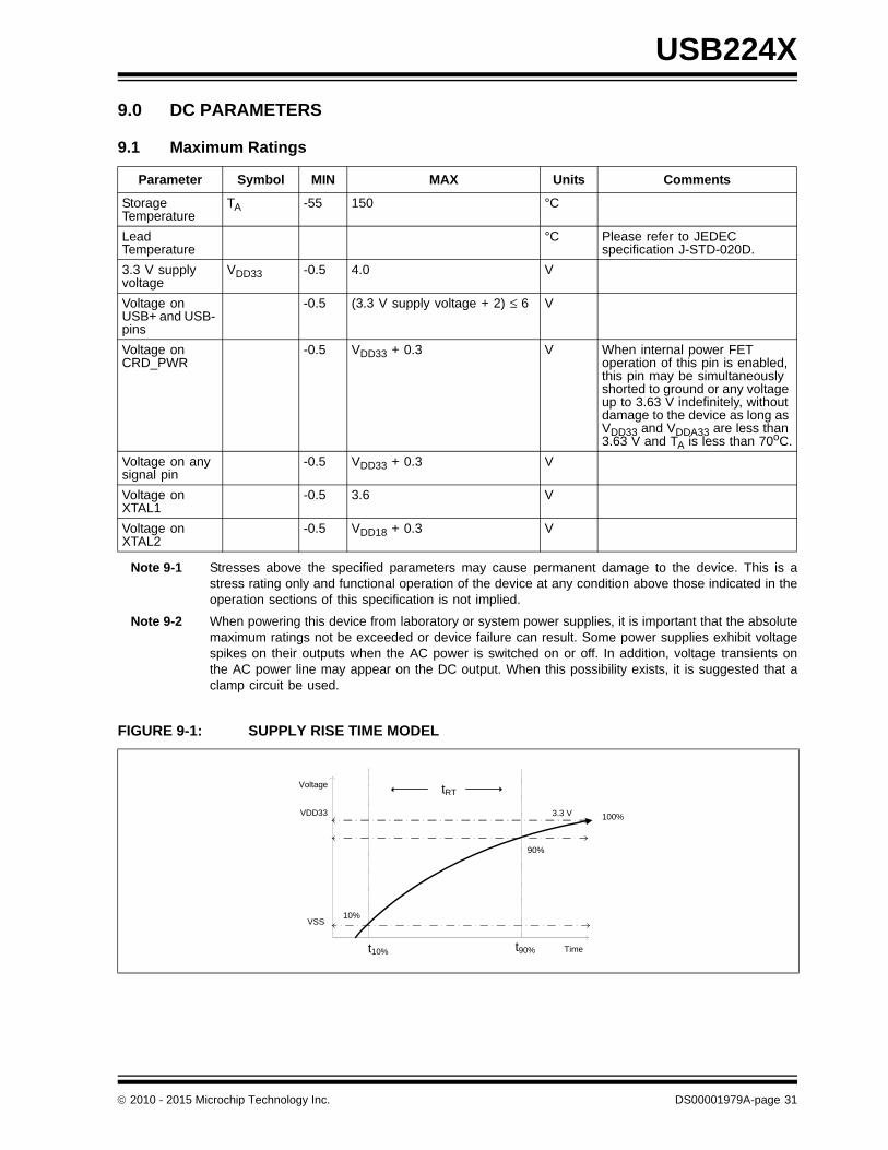
9.0 DC PARAMETERS
9.1 Maximum Ratings
Note 9-1 Stresses above the specified parameters may cause permanent damage to the device. This is astress rating only and functional operation of the device at any condition above those indicated in theoperation sections of this specification is not implied.
Note 9-2 When powering this device from laboratory or system power supplies, it is important that the absolutemaximum ratings not be exceeded or device failure can result. Some power supplies exhibit voltagespikes on their outputs when the AC power is switched on or off. In addition, voltage transients onthe AC power line may appear on the DC output. When this possibility exists, it is suggested that aclamp circuit be used.
Parameter Symbol MIN MAX Units Comments
Storage Temperature
TA -55 150 °C
Lead Temperature
°C Please refer to JEDEC specification J-STD-020D.
3.3 V supply voltage
VDD33 -0.5 4.0 V
Voltage on USB+ and USB- pins
-0.5 (3.3 V supply voltage + 2) ≤ 6 V
Voltage on CRD_PWR
-0.5 VDD33 + 0.3 V When internal power FET operation of this pin is enabled, this pin may be simultaneously shorted to ground or any voltage up to 3.63 V indefinitely, without damage to the device as long as VDD33 and VDDA33 are less than 3.63 V and TA is less than 70oC.
Voltage on any signal pin
-0.5 VDD33 + 0.3 V
Voltage on XTAL1
-0.5 3.6 V
Voltage on XTAL2
-0.5 VDD18 + 0.3 V
FIGURE 9-1: SUPPLY RISE TIME MODEL
t10%
10%
90%
Voltage tRT
t90% Time
100%3.3 V
VSS
VDD33
2010 - 2015 Microchip Technology Inc. DS00001979A-page 31
USB224X
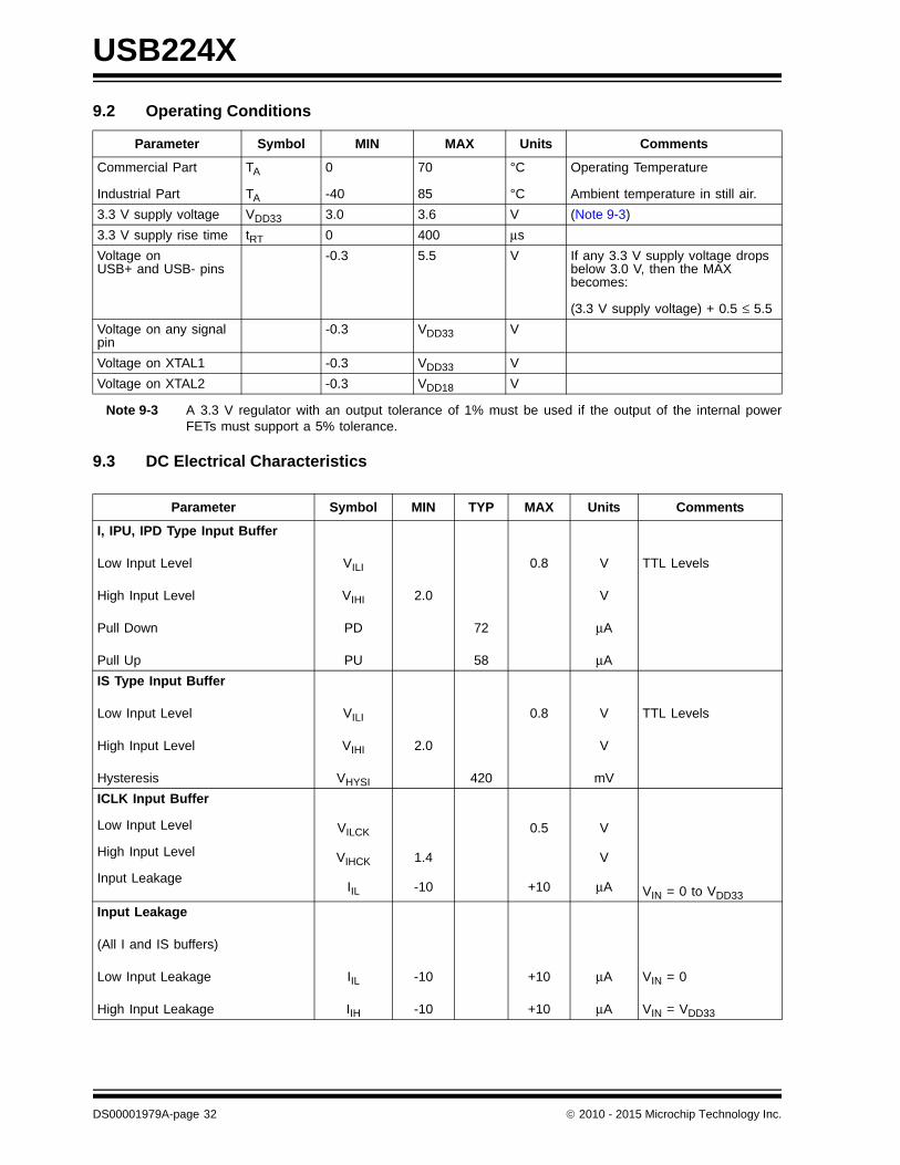
9.2 Operating Conditions
Note 9-3 A 3.3 V regulator with an output tolerance of 1% must be used if the output of the internal powerFETs must support a 5% tolerance.
9.3 DC Electrical Characteristics
Parameter Symbol MIN MAX Units Comments
Commercial Part
Industrial Part
TA
TA
0
-40
70
85
°C
°C
Operating Temperature
Ambient temperature in still air.
3.3 V supply voltage VDD33 3.0 3.6 V (Note 9-3)
3.3 V supply rise time tRT 0 400 μs
Voltage on USB+ and USB- pins
-0.3 5.5 V If any 3.3 V supply voltage drops below 3.0 V, then the MAX becomes:
(3.3 V supply voltage) + 0.5 ≤ 5.5
Voltage on any signal pin
-0.3 VDD33 V
Voltage on XTAL1 -0.3 VDD33 V
Voltage on XTAL2 -0.3 VDD18 V
Parameter Symbol MIN TYP MAX Units Comments
I, IPU, IPD Type Input Buffer
Low Input Level
High Input Level
Pull Down
Pull Up
VILI
VIHI
PD
PU
2.0
72
58
0.8 V
V
μA
μA
TTL Levels
IS Type Input Buffer
Low Input Level
High Input Level
Hysteresis
VILI
VIHI
VHYSI
2.0
420
0.8 V
V
mV
TTL Levels
ICLK Input Buffer
Low Input Level
High Input Level
Input Leakage
VILCK
VIHCK
IIL
1.4
-10
0.5
+10
V
V
μA VIN = 0 to VDD33
Input Leakage
(All I and IS buffers)
Low Input Leakage
High Input Leakage
IIL
IIH
-10
-10
+10
+10
μA
μA
VIN = 0
VIN = VDD33
DS00001979A-page 32 2010 - 2015 Microchip Technology Inc.

USB224X
O12 Type Buffer
Low Output Level
High Output Level
Output Leakage
VOL
VOH
IOL
VDD33- 0.4
-10
0.4
+10
V
V
μA
IOL = 12 mA @ VDD33= 3.3 V
IOH = -12 mA @ VDD33= 3.3 V
VIN = 0 to VDD33(Note 9-4)
I/O12, I/O12PU & I/O12PD Type Buffer
Low Output Level
High Output Level
Output Leakage
Pull Down
Pull Up
VOL
VOH
IOL
PD
PU
VDD33 - 0.4
-10
72
58
0.4
+10
V
V
μA
μA
μA
IOL = 12 mA @ VDD33= 3.3 V
IOH = -12 mA @ VDD33= 3.3 V
VIN = 0 to VDD33(Note 9-4)
IO-U(Note 9-5)
I-R(Note 9-6)
I/O200 Integrated Power FET for CRD_PWR
High Output Current Mode
Low Output Current Mode(Note 9-7)
On Resistance (Note 9-7)
Output Voltage Rise Time
IOUT
IOUT
RDSON
tDSON
200
100
2.1
800
mA
mA
Ω
μs
VdropFET = 0.46 V
VdropFET = 0.23 V
IFET = 70 mA
CLOAD = 10 μF
Supply Current Unconfigured ICCINIT 80 90 mA
Supply Current Active
Full Speed
High Speed
ICC
ICC
110
135
140
165
mA
mA
Supply Current Suspend ICSBY 350 700 µA
Industrial Temperature Suspend ICSBYI 350 900 µA
Parameter Symbol MIN TYP MAX Units Comments
2010 - 2015 Microchip Technology Inc. DS00001979A-page 33

USB224X
Note 9-4 Output leakage is measured with the current pins in high impedance.
Note 9-5 See The USB 2.0 Specification, Chapter 7, for USB DC electrical characteristics
Note 9-6 RBIAS is a 3.3 V tolerant analog pin.
Note 9-7 Output current range is controlled by program software, software disables FET during short circuitcondition.
Note 9-8 The assignment of each Integrated Card Power FET to a designated Card Connector is controlledby both firmware and the specific board implementation.
Note 9-9 The 3.3 V supply should be at least at 75% of its operating condition before the 1.8 V supply isallowed to ramp up.
9.4 Capacitance
TA = 25°C; fc = 1 MHz; VDD, VDDP = 1.8 V
9.5 Package Thermal Specification
Note 9-10 Thermal parameters are measured or estimated for devices with the exposed pad soldered to thermalvias in a multilayer 2S2P PCB per JESD51. Thermal resistance is measured from the die to theambient air.
TABLE 9-1: PIN CAPACITANCE
Parameter SymbolLimits
Unit Test ConditionMIN TYP MAX
Clock Input Capacitance CXTAL 2 pF All pins (except USB pins and pins under test) are tied to AC ground.
Input Capacitance CIN 10 pF
Output Capacitance COUT 20 pF
TABLE 9-2: 36-PIN QFN PACKAGE THERMAL PARAMETERS
ParameterVelocity
(Meters/Sec)Symbol Value Unit
Thermal Resistance 0
ΘJA
33.2
°C/W1 29
2 26
Junction-to-Top-of-Package 0
ΨJT
2.6
°C/W1 2.6
2 2.6
DS00001979A-page 34 2010 - 2015 Microchip Technology Inc.

USB224X
10.0 AC SPECIFICATIONS
10.1 Oscillator/Crystal
Parallel Resonant, Fundamental Mode, 24 MHz ± 350 ppm.
TABLE 10-1: CRYSTAL CIRCUIT LEGEND
Note 10-1 C0 is usually included (subtracted by the crystal manufacturer) in the specification for CL and shouldbe set to ‘0’ for use in the calculation of the capacitance formulas in Figure 10-2, "CapacitanceFormulas". However, the OEM PCB itself may present a parasitic capacitance between XTAL1 andXTAL2. For an accurate calculation of C1 and C2, take the parasitic capacitance between tracesXTAL1 and XTAL2 into account.
Note 10-2 Each of these capacitance values is typically approximately 18 pF.
FIGURE 10-1: TYPICAL CRYSTAL CIRCUIT
SYMBOL DESCRIPTION IN ACCORDANCE WITH
C0 Crystal shunt capacitanceCrystal manufacturer’s specification (See Note 10-1)
CL Crystal load capacitance
CB Total board or trace capacitance OEM board design
CS Stray capacitance MCHP IC and OEM board design
CXTAL XTAL pin input capacitance MCHP IC
C1 Load capacitors installed on OEM board
Calculated values based on Figure 10-2, "Capacitance Formulas" (See Note 10-2)C2
FIGURE 10-2: CAPACITANCE FORMULAS
XTAL1 (CS1 = CB1 + CXTAL1 )
XTAL2 (CS2 = CB2 + CXTAL2 )
C1
C2
CL1 MCrystal
C0
C1 = 2 x (CL – C0) – CS1
C2 = 2 x (CL – C0) – CS2
2010 - 2015 Microchip Technology Inc. DS00001979A-page 35

USB224X
10.2 Ceramic Resonator
24 MHz ± 350 ppm
10.3 External Clock
50% Duty cycle ± 10%, 24 MHz ± 350 ppm, Jitter < 100 ps rms.
The external clock is recommended to conform to the signaling level designated in the JESD76-2 specification on 1.8V CMOS Logic. XTAL2 should be treated as a no connect or drive only a CMOS-like buffer.
FIGURE 10-3: CERAMIC RESONATOR USAGE WITH MCHP IC
XTAL1
XTAL2
1 M24 MHz Ceramic
Resonator
DS00001979A-page 36 2010 - 2015 Microchip Technology Inc.

USB224X
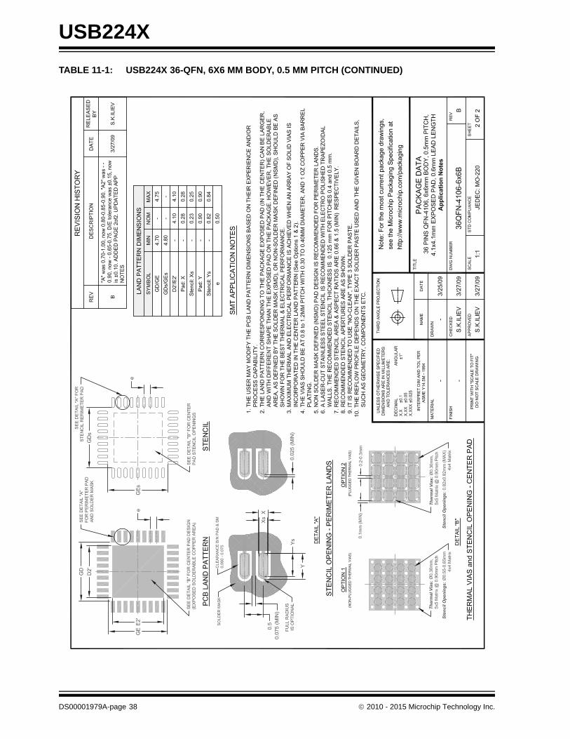
11.0 PACKAGE OUTLINE
TABLE 11-1: USB224X 36-QFN, 6X6 MM BODY, 0.5 MM PITCH
Not
e: F
or th
e m
ost c
urre
nt p
acka
ge d
raw
ings
, se
e th
e M
icro
chip
Pac
kagi
ng S
peci
ficat
ion
at
http
://w
ww
.mic
roch
ip.c
om/p
acka
ging
2010 - 2015 Microchip Technology Inc. DS00001979A-page 37
USB224X
TABLE 11-1: USB224X 36-QFN, 6X6 MM BODY, 0.5 MM PITCH (CONTINUED)
Not
e: F
or th
e m
ost c
urre
nt p
acka
ge d
raw
ings
, se
e th
e M
icro
chip
Pac
kagi
ng S
peci
ficat
ion
at
http
://w
ww
.mic
roch
ip.c
om/p
acka
ging
DS00001979A-page 38 2010 - 2015 Microchip Technology Inc.

2010 - 2015 Microchip Technology Inc. DS00001979A-page 39
USB224X
APPENDIX A: DATA SHEET REVISION HISTORY
TABLE A-1: REVISION HISTORY
REVISION SECTION/FIGURE/ENTRY CORRECTION
DS00001979A (07-13-15) Replaces previous SMSC version Rev. 2.1 (02-07-13)
GPIOs and SDIO support removed
USB2242 removed
Rev. 2.1(02-07-13)
Document co-branded: Microchip logo added to cover; company disclaimer modified.
Added the following to the ordering information: “Please contact your SMSC sales representative for additional documentation related to this product such as application notes, anomaly sheets, and design guidelines.”
Rev 2.1(12-22-10)
Chapter 3, Figure 3.1, 3.2, and 3.3
Upgraded to put the mux for the multiplexed interface inside the part, put in a SPI interface for outside access to the Program Memory I/O bus.
Rev 2.1(11-23-10)
Chapter 6, Table 6.1 Removed “ It may not be used to drive any external circuitry other than the crystal circuit” from the XTAL2 description.
Rev. 2.1(10-21-10)
Chapter 11, Table 11.3 Changed the active level from L to H for GPIO6.

USB224X
DS00001979A-page 40 2010 - 2015 Microchip Technology Inc.
THE MICROCHIP WEB SITE
Microchip provides online support via our WWW site at www.microchip.com. This web site is used as a means to makefiles and information easily available to customers. Accessible by using your favorite Internet browser, the web site con-tains the following information:
• Product Support – Data sheets and errata, application notes and sample programs, design resources, user’s guides and hardware support documents, latest software releases and archived software
• General Technical Support – Frequently Asked Questions (FAQ), technical support requests, online discussion groups, Microchip consultant program member listing
• Business of Microchip – Product selector and ordering guides, latest Microchip press releases, listing of semi-nars and events, listings of Microchip sales offices, distributors and factory representatives
CUSTOMER CHANGE NOTIFICATION SERVICE
Microchip’s customer notification service helps keep customers current on Microchip products. Subscribers will receivee-mail notification whenever there are changes, updates, revisions or errata related to a specified product family ordevelopment tool of interest.
To register, access the Microchip web site at www.microchip.com. Under “Support”, click on “Customer Change Notifi-cation” and follow the registration instructions.
CUSTOMER SUPPORT
Users of Microchip products can receive assistance through several channels:
• Distributor or Representative
• Local Sales Office
• Field Application Engineer (FAE)
• Technical Support
Customers should contact their distributor, representative or field application engineer (FAE) for support. Local salesoffices are also available to help customers. A listing of sales offices and locations is included in the back of this docu-ment.
Technical support is available through the web site at: http://www.microchip.com/support
2010 - 2015 Microchip Technology Inc. DS00001979A-page 41
USB224X
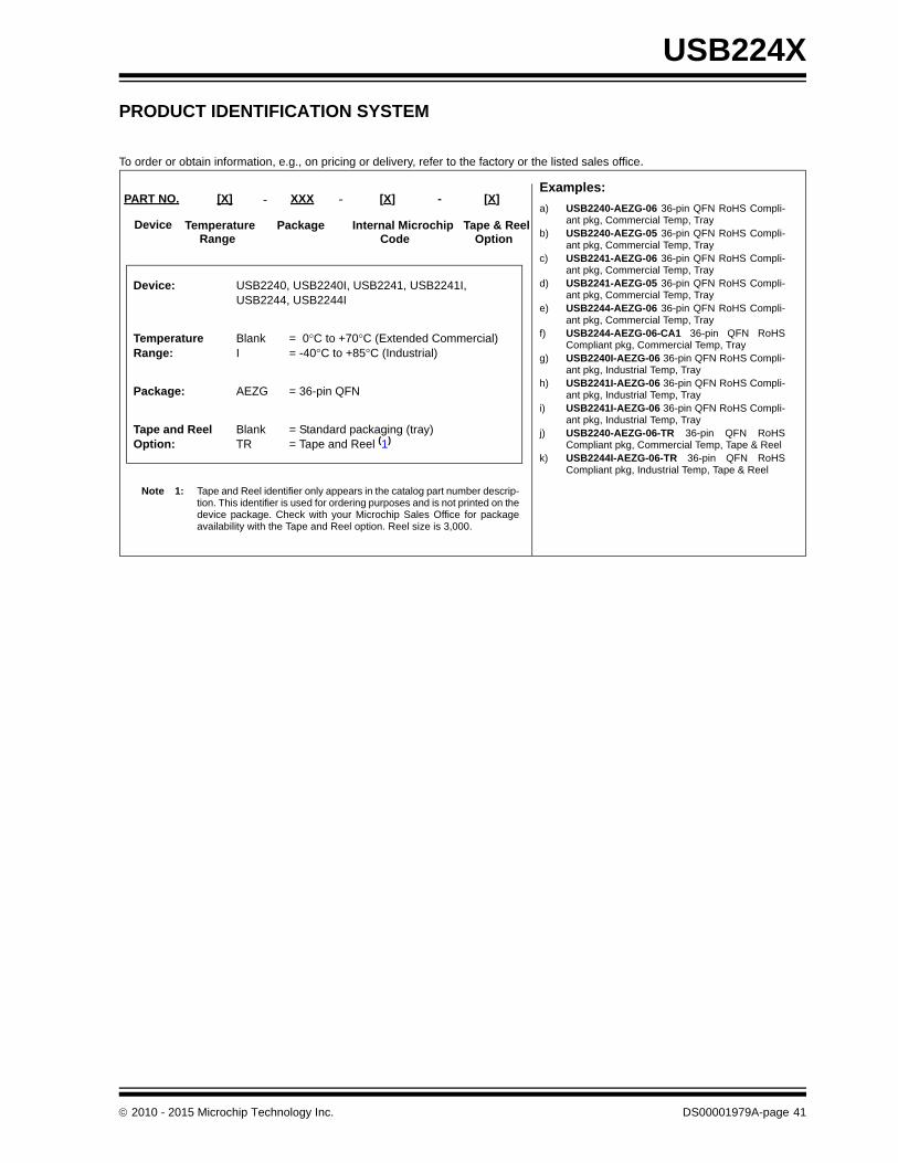
PRODUCT IDENTIFICATION SYSTEM
To order or obtain information, e.g., on pricing or delivery, refer to the factory or the listed sales office.
Device: USB2240, USB2240I, USB2241, USB2241I, USB2244, USB2244I
Temperature Range:
Blank = 0°C to +70°C (Extended Commercial)I = -40°C to +85°C (Industrial)
Package: AEZG = 36-pin QFN
Tape and Reel Option:
Blank = Standard packaging (tray)TR = Tape and Reel (1)
Note 1: Tape and Reel identifier only appears in the catalog part number descrip-tion. This identifier is used for ordering purposes and is not printed on thedevice package. Check with your Microchip Sales Office for packageavailability with the Tape and Reel option. Reel size is 3,000.
PART NO. [X] XXX
PackageTemperatureRange
Device
[X] - [X]
Internal Microchip Tape & Reel Code Option
- -Examples:
a) USB2240-AEZG-06 36-pin QFN RoHS Compli-ant pkg, Commercial Temp, Tray
b) USB2240-AEZG-05 36-pin QFN RoHS Compli-ant pkg, Commercial Temp, Tray
c) USB2241-AEZG-06 36-pin QFN RoHS Compli-ant pkg, Commercial Temp, Tray
d) USB2241-AEZG-05 36-pin QFN RoHS Compli-ant pkg, Commercial Temp, Tray
e) USB2244-AEZG-06 36-pin QFN RoHS Compli-ant pkg, Commercial Temp, Tray
f) USB2244-AEZG-06-CA1 36-pin QFN RoHSCompliant pkg, Commercial Temp, Tray
g) USB2240I-AEZG-06 36-pin QFN RoHS Compli-ant pkg, Industrial Temp, Tray
h) USB2241I-AEZG-06 36-pin QFN RoHS Compli-ant pkg, Industrial Temp, Tray
i) USB2241I-AEZG-06 36-pin QFN RoHS Compli-ant pkg, Industrial Temp, Tray
j) USB2240-AEZG-06-TR 36-pin QFN RoHSCompliant pkg, Commercial Temp, Tape & Reel
k) USB2244I-AEZG-06-TR 36-pin QFN RoHSCompliant pkg, Industrial Temp, Tape & Reel

USB224X
DS00001979A-page 42 2010 - 2015 Microchip Technology Inc.
Note the following details of the code protection feature on Microchip devices:
• Microchip products meet the specification contained in their particular Microchip Data Sheet.
• Microchip believes that its family of products is one of the most secure families of its kind on the market today, when used in the intended manner and under normal conditions.
• There are dishonest and possibly illegal methods used to breach the code protection feature. All of these methods, to our knowledge, require using the Microchip products in a manner outside the operating specifications contained in Microchip’s Data Sheets. Most likely, the person doing so is engaged in theft of intellectual property.
• Microchip is willing to work with the customer who is concerned about the integrity of their code.
• Neither Microchip nor any other semiconductor manufacturer can guarantee the security of their code. Code protection does not mean that we are guaranteeing the product as “unbreakable.”
Code protection is constantly evolving. We at Microchip are committed to continuously improving the code protection features of ourproducts. Attempts to break Microchip’s code protection feature may be a violation of the Digital Millennium Copyright Act. If such actsallow unauthorized access to your software or other copyrighted work, you may have a right to sue for relief under that Act.
Microchip received ISO/TS-16949:2009 certification for its worldwide headquarters, design and wafer fabrication facilities in Chandler and Tempe, Arizona; Gresham, Oregon and design centers in California and India. The Company’s quality system processes and procedures are for its PIC® MCUs and dsPIC® DSCs, KEELOQ® code hopping devices, Serial EEPROMs, microperipherals, nonvolatile memory and analog products. In addition, Microchip’s quality system for the design and manufacture of development systems is ISO 9001:2000 certified.
QUALITY MANAGEMENT SYSTEM CERTIFIED BY DNV
== ISO/TS 16949 ==
Information contained in this publication regarding device applications and the like is provided only for your convenience and may besuperseded by updates. It is your responsibility to ensure that your application meets with your specifications. MICROCHIP MAKES NOREPRESENTATIONS OR WARRANTIES OF ANY KIND WHETHER EXPRESS OR IMPLIED, WRITTEN OR ORAL, STATUTORY OROTHERWISE, RELATED TO THE INFORMATION, INCLUDING BUT NOT LIMITED TO ITS CONDITION, QUALITY, PERFORMANCE,MERCHANTABILITY OR FITNESS FOR PURPOSE. Microchip disclaims all liability arising from this information and its use. Use of Micro-chip devices in life support and/or safety applications is entirely at the buyer’s risk, and the buyer agrees to defend, indemnify and holdharmless Microchip from any and all damages, claims, suits, or expenses resulting from such use. No licenses are conveyed, implicitly orotherwise, under any Microchip intellectual property rights unless otherwise stated.
Trademarks
The Microchip name and logo, the Microchip logo, dsPIC, FlashFlex, flexPWR, JukeBlox, KEELOQ, KEELOQ logo, Kleer, LANCheck, MediaLB, MOST, MOST logo, MPLAB, OptoLyzer, PIC, PICSTART, PIC32 logo, RightTouch, SpyNIC, SST, SST Logo, SuperFlash and UNI/O are registered trademarks of Microchip Technology Incorporated in the U.S.A. and other countries.
The Embedded Control Solutions Company and mTouch are registered trademarks of Microchip Technology Incorporated in the U.S.A.
Analog-for-the-Digital Age, BodyCom, chipKIT, chipKIT logo, CodeGuard, dsPICDEM, dsPICDEM.net, ECAN, In-Circuit Serial Programming, ICSP, Inter-Chip Connectivity, KleerNet, KleerNet logo, MiWi, MPASM, MPF, MPLAB Certified logo, MPLIB, MPLINK, MultiTRAK, NetDetach, Omniscient Code Generation, PICDEM, PICDEM.net, PICkit, PICtail, RightTouch logo, REAL ICE, SQI, Serial Quad I/O, Total Endurance, TSHARC, USBCheck, VariSense, ViewSpan, WiperLock, Wireless DNA, and ZENA are trademarks of Microchip Technology Incorporated in the U.S.A. and other countries.
SQTP is a service mark of Microchip Technology Incorporated in the U.S.A.
Silicon Storage Technology is a registered trademark of Microchip Technology Inc. in other countries.
GestIC is a registered trademarks of Microchip Technology Germany II GmbH & Co. KG, a subsidiary of Microchip Technology Inc., in other countries.
All other trademarks mentioned herein are property of their respective companies.
© 2010 - 2015, Microchip Technology Incorporated, Printed in the U.S.A., All Rights Reserved.
ISBN: 9781632775665

2010 - 2015 Microchip Technology Inc. DS00001979A-page 43
AMERICASCorporate Office2355 West Chandler Blvd.Chandler, AZ 85224-6199Tel: 480-792-7200 Fax: 480-792-7277Technical Support: http://www.microchip.com/supportWeb Address: www.microchip.com
AtlantaDuluth, GA Tel: 678-957-9614 Fax: 678-957-1455
Austin, TXTel: 512-257-3370
BostonWestborough, MA Tel: 774-760-0087 Fax: 774-760-0088
ChicagoItasca, IL Tel: 630-285-0071 Fax: 630-285-0075
ClevelandIndependence, OH Tel: 216-447-0464 Fax: 216-447-0643
DallasAddison, TX Tel: 972-818-7423 Fax: 972-818-2924
DetroitNovi, MI Tel: 248-848-4000
Houston, TX Tel: 281-894-5983
IndianapolisNoblesville, IN Tel: 317-773-8323Fax: 317-773-5453
Los AngelesMission Viejo, CA Tel: 949-462-9523 Fax: 949-462-9608
New York, NY Tel: 631-435-6000
San Jose, CA Tel: 408-735-9110
Canada - TorontoTel: 905-673-0699 Fax: 905-673-6509
ASIA/PACIFICAsia Pacific OfficeSuites 3707-14, 37th FloorTower 6, The GatewayHarbour City, KowloonHong KongTel: 852-2943-5100Fax: 852-2401-3431
Australia - SydneyTel: 61-2-9868-6733Fax: 61-2-9868-6755
China - BeijingTel: 86-10-8569-7000 Fax: 86-10-8528-2104
China - ChengduTel: 86-28-8665-5511Fax: 86-28-8665-7889
China - ChongqingTel: 86-23-8980-9588Fax: 86-23-8980-9500
China - Dongguan
Tel: 86-769-8702-9880
China - HangzhouTel: 86-571-8792-8115 Fax: 86-571-8792-8116
China - Hong Kong SARTel: 852-2943-5100 Fax: 852-2401-3431
China - NanjingTel: 86-25-8473-2460Fax: 86-25-8473-2470
China - QingdaoTel: 86-532-8502-7355Fax: 86-532-8502-7205
China - ShanghaiTel: 86-21-5407-5533 Fax: 86-21-5407-5066
China - ShenyangTel: 86-24-2334-2829Fax: 86-24-2334-2393
China - ShenzhenTel: 86-755-8864-2200 Fax: 86-755-8203-1760
China - WuhanTel: 86-27-5980-5300Fax: 86-27-5980-5118
China - XianTel: 86-29-8833-7252Fax: 86-29-8833-7256
ASIA/PACIFICChina - XiamenTel: 86-592-2388138 Fax: 86-592-2388130
China - ZhuhaiTel: 86-756-3210040 Fax: 86-756-3210049
India - BangaloreTel: 91-80-3090-4444 Fax: 91-80-3090-4123
India - New DelhiTel: 91-11-4160-8631Fax: 91-11-4160-8632
India - PuneTel: 91-20-3019-1500
Japan - OsakaTel: 81-6-6152-7160 Fax: 81-6-6152-9310
Japan - TokyoTel: 81-3-6880- 3770 Fax: 81-3-6880-3771
Korea - DaeguTel: 82-53-744-4301Fax: 82-53-744-4302
Korea - SeoulTel: 82-2-554-7200Fax: 82-2-558-5932 or 82-2-558-5934
Malaysia - Kuala LumpurTel: 60-3-6201-9857Fax: 60-3-6201-9859
Malaysia - PenangTel: 60-4-227-8870Fax: 60-4-227-4068
Philippines - ManilaTel: 63-2-634-9065Fax: 63-2-634-9069
SingaporeTel: 65-6334-8870Fax: 65-6334-8850
Taiwan - Hsin ChuTel: 886-3-5778-366Fax: 886-3-5770-955
Taiwan - KaohsiungTel: 886-7-213-7828
Taiwan - TaipeiTel: 886-2-2508-8600 Fax: 886-2-2508-0102
Thailand - BangkokTel: 66-2-694-1351Fax: 66-2-694-1350
EUROPEAustria - WelsTel: 43-7242-2244-39Fax: 43-7242-2244-393Denmark - CopenhagenTel: 45-4450-2828 Fax: 45-4485-2829
France - ParisTel: 33-1-69-53-63-20 Fax: 33-1-69-30-90-79
Germany - DusseldorfTel: 49-2129-3766400
Germany - MunichTel: 49-89-627-144-0 Fax: 49-89-627-144-44
Germany - PforzheimTel: 49-7231-424750
Italy - Milan Tel: 39-0331-742611 Fax: 39-0331-466781
Italy - VeniceTel: 39-049-7625286
Netherlands - DrunenTel: 31-416-690399 Fax: 31-416-690340
Poland - WarsawTel: 48-22-3325737
Spain - MadridTel: 34-91-708-08-90Fax: 34-91-708-08-91
Sweden - StockholmTel: 46-8-5090-4654
UK - WokinghamTel: 44-118-921-5800Fax: 44-118-921-5820
Worldwide Sales and Service
01/27/15