use of approximate triple modular redundancy for fault
TRANSCRIPT
DEPARTAMENTO DE TECNOLOGÍA INFORMÁTICA Y COMPUTACION
Tesis en contutela con la
UNIVERSIDADE FEDERAL DO RIO GRANDE DO SUL (UFRGS)
Use of Approximate Triple ModularRedundancy for Fault Tolerance in
Digital CircuitsIuri Albandes Cunha Gomes
Tesis presentada para aspirar al grado de
DOCTOR POR LA UNIVERSIDAD DE ALICANTE
PROGRAMA DE DOCTORADO EN INFORMATICA
Directores
Dr. Sergio Cuenca-Asensi
Dr. Fernanda Gusmão de Lima Kastensmidt
Agosto 2018

UNIVERSIDADE FEDERAL DO RIO GRANDE DO SULINSTITUTO DE INFORMÁTICA
PROGRAMA DE PÓS-GRADUAÇÃO EM MICROELETRÔNICA
IURI ALBANDES CUNHA GOMES
Use of Approximate Triple ModularRedundancy for Fault Tolerance in Digital
Circuits
Thesis presented in partial fulfillmentof the requirements for the degree ofDoctor of Microeletronics
Advisor: Prof. Dr. Fernanda KastensmidtCoadvisor: Prof. Dr. Sergio Cuenca
Porto AlegreAugust 2018
CIP — CATALOGING-IN-PUBLICATION
Albandes Cunha Gomes, Iuri
Use of Approximate Triple Modular Redundancy for FaultTolerance in Digital Circuits / Iuri Albandes Cunha Gomes. –Porto Alegre: PGMICRO da UFRGS, 2018.
140 f.: il.
Thesis (Ph.D.) – Universidade Federal do Rio Grande do Sul.Programa de Pós-Graduação em Microeletrônica, Porto Alegre,BR–RS, 2018. Advisor: Fernanda Kastensmidt; Coadvisor: Ser-gio Cuenca.
1. Approximate Circuits. 2. Approximate-TMR. 3. Multi-Objective Optimization Genetic Algorithm. 4. Fault Tolerance.5. Single Event Effects. I. Kastensmidt, Fernanda. II. Cuenca,Sergio. III. Título.
UNIVERSIDADE FEDERAL DO RIO GRANDE DO SULReitor: Prof. Rui Vicente OppermannVice-Reitora: Profa. Jane Fraga TutikianPró-Reitor de Pós-Graduação: Prof. Celso Giannetti Loureiro ChavesDiretora do Instituto de Informática: Profa. Carla Maria Dal Sasso FreitasCoordenadora do PGMICRO: Prof. Fernanda Gusmão de Lima KastensmidtBibliotecária-chefe do Instituto de Informática: Beatriz Regina Bastos Haro
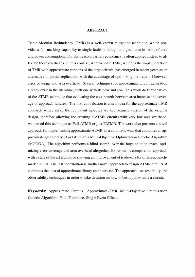
ABSTRACT
Triple Modular Redundancy (TMR) is a well-known mitigation technique, which pro-
vides a full masking capability to single faults, although at a great cost in terms of area
and power consumption. For that reason, partial redundancy is often applied instead to al-
leviate these overheads. In this context, Approximate TMR, which is the implementation
of TMR with approximate versions of the target circuit, has emerged in recent years as an
alternative to partial replication, with the advantage of optimizing the trade-off between
error coverage and area overhead. Several techniques for approximate circuit generation
already exist in the literature, each one with its pros and con. This work do further study
of the ATMR technique that evaluating the cost-benefit between area increase and cover-
age of approach failures. The first contribution is a new idea for the approximate-TMR
approach where all of the redundant modules are approximate version of the original
design, therefore allowing the creating o ATMR circuits with very low area overhead,
we named this technique as Full-ATMR or just FATMR. The work also presents a novel
approach for implementing approximate ATMR, in a automatic way, that combines an ap-
proximate gate library (ApxLib) with a Multi-Objective Optimization Genetic Algorithm
(MOOGA). The algorithm performs a blind search, over the huge solution space, opti-
mizing error coverage and area overhead altogether. Experiments compare our approach
with a state of the art technique showing an improvement of trade-offs for different bench-
mark circuits. The last contribution is another novel approach to design ATMR circuits, it
combines the idea of approximate library and heuristic. The approach uses testability and
observability techniques in order to take decision on how to best approximate a circuit.
Keywords: Approximate Circuits. Approximate-TMR. Multi-Objective Optimization
Genetic Algorithm. Fault Tolerance. Single Event Effects.
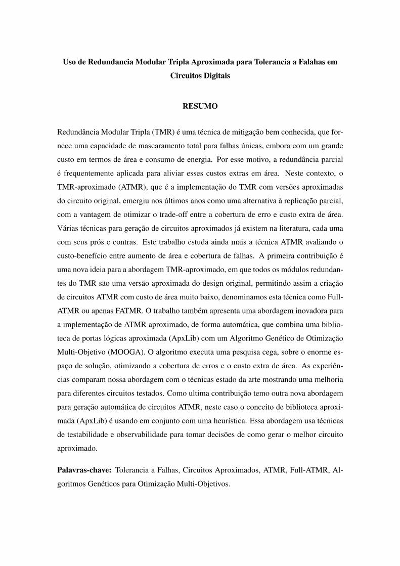
Uso de Redundancia Modular Tripla Aproximada para Tolerancia a Falahas em
Circuitos Digitais
RESUMO
Redundância Modular Tripla (TMR) é uma técnica de mitigação bem conhecida, que for-
nece uma capacidade de mascaramento total para falhas únicas, embora com um grande
custo em termos de área e consumo de energia. Por esse motivo, a redundância parcial
é frequentemente aplicada para aliviar esses custos extras em área. Neste contexto, o
TMR-aproximado (ATMR), que é a implementação do TMR com versões aproximadas
do circuito original, emergiu nos últimos anos como uma alternativa à replicação parcial,
com a vantagem de otimizar o trade-off entre a cobertura de erro e custo extra de área.
Várias técnicas para geração de circuitos aproximados já existem na literatura, cada uma
com seus prós e contras. Este trabalho estuda ainda mais a técnica ATMR avaliando o
custo-benefício entre aumento de área e cobertura de falhas. A primeira contribuição é
uma nova ideia para a abordagem TMR-aproximado, em que todos os módulos redundan-
tes do TMR são uma versão aproximada do design original, permitindo assim a criação
de circuitos ATMR com custo de área muito baixo, denominamos esta técnica como Full-
ATMR ou apenas FATMR. O trabalho também apresenta uma abordagem inovadora para
a implementação de ATMR aproximado, de forma automática, que combina uma biblio-
teca de portas lógicas aproximada (ApxLib) com um Algoritmo Genético de Otimização
Multi-Objetivo (MOOGA). O algoritmo executa uma pesquisa cega, sobre o enorme es-
paço de solução, otimizando a cobertura de erros e o custo extra de área. As experiên-
cias comparam nossa abordagem com o técnicas estado da arte mostrando uma melhoria
para diferentes circuitos testados. Como ultima contribuição temo outra nova abordagem
para geração automática de circuitos ATMR, neste caso o conceito de biblioteca aproxi-
mada (ApxLib) é usando em conjunto com uma heurística. Essa abordagem usa técnicas
de testabilidade e observabilidade para tomar decisões de como gerar o melhor circuito
aproximado.
Palavras-chave: Tolerancia a Falhas, Circuitos Aproximados, ATMR, Full-ATMR, Al-
goritmos Genéticos para Otimização Multi-Objetivos.

LIST OF ABBREVIATIONS AND ACRONYMS
ATMR Approximate Triple Modular Redudancy
ApxLib Approximate Library
CGP Cartesian Genetic Programming
DUT Design Under Test
DWC Duplication With Comparison
FATMR Full Approximate Triple Modular Redudancy
GP Genetic Programming
HDL Hardware Level Language
IC Integrated Circuit
MOOGA Multi-Objective Optimization Genetic Algorithm
NMR N-tuple Modular Redundancy
RTL Register Transfer Level
SEE Single-Event Effect
SEL Single-Event Latch-up
SET Single-Event Transient
SEU Single-Event Upset
TID Total Ionizing Dose
TMR Triple Modular Redudancy

LIST OF FIGURES
Figure 1.1 Moore’s law fitting in the period 1971–2011. (GUARNIERI, 2016)............13
Figure 2.1 Charge collection mechanism for a SEE. ......................................................18Figure 2.2 Charge generation and collection phases in a reverse-biased junction
and the resultant current pulse caused by the passage of a high-energy ion.(BAUMANN, 2005)...............................................................................................19
Figure 2.3 Single event upset in different types of memory elements. (MUNTEANU;AUTRAN, 2008)....................................................................................................20
Figure 2.4 Logical masking. Adapted from (MUNTEANU; AUTRAN, 2008).............21Figure 2.5 Electrical masking. Adapted from (MUNTEANU; AUTRAN, 2008)..........22Figure 2.6 Temporal masking. Adapted from (MUNTEANU; AUTRAN, 2008)..........22Figure 2.7 Logic level simulation of a SET (MUNTEANU; AUTRAN, 2008) .............23Figure 2.8 Electric level simulation of a SEE. ................................................................24Figure 2.9 SRAM cell 3D simulation. (MUNTEANU; AUTRAN, 2008) .....................25Figure 2.10 Mixed-mode simulations. (MUNTEANU; AUTRAN, 2008).....................26
Figure 3.1 TMR scheme..................................................................................................28Figure 3.2 Majority voter circuit. ....................................................................................28Figure 3.3 Majority voter circuit. ....................................................................................28Figure 3.4 Majority voter circuit. ....................................................................................29Figure 3.5 Minterms relationship between functions G and H .......................................31Figure 3.6 Minterms relationship between functions G and F........................................32Figure 3.7 ATMR scheme composed by one original module and two approxi-
mated modules (F and H).......................................................................................36Figure 3.8 Illustration of the F ⊆ G ⊆ H relation. Gray area represent the G =
F = H state. White are shows the G = F 6= H and G = H 6= F states..............37Figure 3.9 Vectors, minterms and maxterms analysis.....................................................41Figure 3.10 Unidirectional fault approximation examples. ............................................44Figure 3.11 Cartesian genetic programming schema. (SANCHEZ-CLEMENTE et
al., 2016) ................................................................................................................45Figure 3.12 CGP individual example. (SANCHEZ-CLEMENTE et al., 2016) .............46
Figure 4.1 Z is a non comparable function. ....................................................................48Figure 4.2 Functions needed to compose the G function................................................49Figure 4.3 Candidate functions to compose the F and H function..................................49Figure 4.4 Graphical representation of the relationship of functions for a Full-ATMR
composed by F1,F2 and Hx. Grey area is protected, i.e, all functions convergeto the same value....................................................................................................52
Figure 4.5 Graphical representation of the relationship of functions for a Full-ATMRcomposed by Fx, H1 and H2. Grey area is protected, i.e, all functions con-verge to the same value. .........................................................................................54
Figure 4.6 Graphical representation of the relationship of functions for a Full-ATMRonly by F functions or H functions. Grey area is protected, i.e, all functionsconverge to the same value. ...................................................................................54
Figure 4.7 Methodology used to generate results for ATMR/FATMR circuits...............55Figure 4.8 4-bit Ripple-carry adder with TMR/ATMR...................................................58
Figure 5.1 Approximate library approach: each cell can be replaced by an approx-imated gate from the library. .................................................................................62
Figure 5.2 Approximate library approach: approximations possibilities for g1 XOR2gate. .......................................................................................................................63
Figure 5.3 Approximate library approach: approximations possibilities for g2 andg3 gates. .................................................................................................................63
Figure 5.4 Karnaugh map for the final over-approximate functions of G. .....................64Figure 5.5 Karnaugh map for the final under-approximate functions of G. ...................64Figure 5.6 Parity analysis example. ...............................................................................66Figure 5.7 Approximate library approach, where each cell can be replaced by an
approximate function from the library. .................................................................67Figure 5.8 Karnaugh map for the final under-approximate functions of G. ...................68Figure 5.9 Karnaugh map for the final under-approximate functions of G. ...................68Figure 5.10 Approximate library approach, where each cell can be replaced by an
approximate function from the library. .................................................................69Figure 5.11 Approximate library approach, where each cell can be replaced by an
approximate function from the library. .................................................................70Figure 5.12 Karnaugh map for the final under-approximate functions of G. .................70Figure 5.13 Approximate library approach, where each cell can be replaced by an
approximate function from the library. .................................................................70Figure 5.14 Approximate library approach, where each cell can be replaced by an
approximate function from the library. .................................................................71Figure 5.15 Karnaugh map for the final under-approximate functions of G. .................71
Figure 6.1 Exponential growth of solution for the ApxLib approach.............................73Figure 6.2 Original circuit G...........................................................................................74Figure 6.3 Original circuit G chromosomes. ..................................................................75Figure 6.4 Over-approximated individual genotype created by mutation.......................77Figure 6.5 Under-approximated individual genotype created by mutation ....................78Figure 6.6 Single point crossover....................................................................................78Figure 6.7 Circuit G informations...................................................................................79Figure 6.8 Circuit ATMR1 informations. ........................................................................80Figure 6.9 Circuit ATMR2 informations. ........................................................................80Figure 6.10 Single point crossover example. ..................................................................80Figure 6.11 Pareto-front of a Min–Min problem ............................................................81Figure 6.12 Population Sorting and Selection using NSGA2.........................................82Figure 6.13 MOOGA+ApxLib Algorithm flow..............................................................83Figure 6.14 ATMR population for benchmark newtag ...................................................85Figure 6.15 ATMR population for benchmark majority .................................................85Figure 6.16 ATMR population for benchmark clpl.........................................................86Figure 6.17 ATMR population for benchmark cm82a....................................................86Figure 6.18 ATMR population for benchmark rd73 .......................................................87Figure 6.19 3d plot for benchmark newtag .....................................................................88Figure 6.20 3d plot for benchmark majority ...................................................................88Figure 6.21 3d plot for benchmark clpl...........................................................................89Figure 6.22 3d plot for benchmark cm82a......................................................................90Figure 6.23 3d plot for benchmark rd73 .........................................................................90Figure 6.24 Results for benchmark newtag: comparison between approaches ..............91Figure 6.25 Results for benchmark majority: comparison between approaches ............91Figure 6.26 Results for benchmark clpl: comparison between approaches....................92Figure 6.27 Results for benchmark cm82a: comparison between approaches ...............92Figure 6.28 Results for benchmark rd73: comparison between approaches ..................93
Figure 7.1 Circuit c1 .......................................................................................................95Figure 7.2 Correlation graph for benchmark majority ....................................................97Figure 7.3 Correlation graph for benchmark newtag ......................................................97Figure 7.4 Correlation graph for benchmark rd73 ..........................................................98Figure 7.5 Correlation graph for benchmark t481 ..........................................................98Figure 7.6 Circuit c1 over-approximations .....................................................................99Figure 7.7 Heuristic approach 1 flowchart (small circuits)...........................................101Figure 7.8 Heuristic approach 2 flowchart (larger circuits) ..........................................102Figure 7.9 Comparison between ATMR generated by heuristic and genetic approaches
for the circuit majority..........................................................................................104Figure 7.10 Comparison between ATMR generated by heuristic and genetic ap-
proaches for the circuit clpl..................................................................................105Figure 7.11 Comparison between ATMR generated by heuristic and genetic ap-
proaches for the circuit cm82a. ............................................................................106Figure 7.12 Comparison between ATMR generated by heuristic and genetic ap-
proaches for the circuit rd73. ...............................................................................106
Figure A.1 Representación gráfica de la relación de funciones para un Full-ATMRcompuesto por dos funciones sub-aproximadas y una sobre-aproximada. Elárea gris está protegida, es decir, todas las funciones convergen al mismo valor.117
Figure A.2 Representación gráfica de la relación de funciones para un Full-ATMRcompuesto por dos funciones sobre-aproximadas y una sub-aproximada. Elárea gris está protegida, es decir, todas las funciones convergen al mismo valor.118
Figure A.3 Representación gráfica de la relación de funciones para un Full-ATMRsolo mediante funciones F o funciones H. El área gris está protegida, es decir,todas las funciones convergen al mismo valor .....................................................118
Figure A.4 Z is a non comparable function. .................................................................119Figure A.5 Biblioteca approximada: cada puerta lógica puede ser reemplazada por
una puerta aproximada de la biblioteca. .............................................................121Figure A.6 Mapa de Karnaugh para las funciones sobre-aproximadas finales de G. ...122Figure A.7 Mapa de Karnaugh para las funciones sub-aproximadas finales de G. ......123Figure A.8 MOOGA+ApxLib Algorithm flow.............................................................125Figure A.9 Original circuit G........................................................................................126Figure A.10 Original circuit G chromosomes...............................................................126Figure A.11 Single point crossover. ..............................................................................128Figure A.12 pasos del enfoque heurístico. ....................................................................130Figure A.13 Resultados para el benchmark newtag: comparación entre enfoques ......131Figure A.14 Resultados para el benchmark majority: comparación entre enfoques ....131Figure A.15 Resultados para el benchmark clpl: comparación entre enfoques............132Figure A.16 Resultados para el benchmark cm82a: comparación entre enfoques .......132Figure A.17 Resultados para el benchmark rd73: comparación entre enfoques ..........133Figure A.18 Comparación entre ATMR generada por aproximaciones heurísticas y
genéticas para el circuito majority. ......................................................................135Figure A.19 Comparación entre ATMR generada por aproximaciones heurísticas y
genéticas para el circuito clpl...............................................................................135Figure A.20 Comparación entre ATMR generada por aproximaciones heurísticas y
genéticas para el circuito cm82a. .........................................................................136Figure A.21 Comparación entre ATMR generada por aproximaciones heurísticas y
genéticas para el circuito rd73. ............................................................................137
LIST OF TABLES
Table 3.1 Example of G ⊆ H relation ............................................................................31Table 3.2 Example of F ⊆ G relation.............................................................................32Table 3.3 Truth table of G and its over-approximated functions (H1, H2 and H3).........34Table 3.4 Truth table of G and its under-approximated functions (F1, F2 and F3).........35Table 3.5 Size and convergence for approximated functions derived from G = A ∗
(B + C) .................................................................................................................35Table 3.6 Truth table for a ATMR scheme......................................................................37Table 3.7 Truth table of a ATMR scheme. Fault in one of the modules while in a
protected vectors. ...................................................................................................38Table 3.8 Truth table of a ATMR scheme. Fault in H module during a G = F 6= H
state. .......................................................................................................................39Table 3.9 Truth table of a ATMR scheme. Fault in G module during a G = F 6= H
state. .......................................................................................................................39Table 3.10 Truth table of a ATMR scheme. Fault in F module during a G = H 6= F
state. .......................................................................................................................40Table 3.11 Truth table of a ATMR scheme. Fault in H module during a G = F 6=
H state....................................................................................................................41
Table 4.1 Not comparable relation example....................................................................48Table 4.2 Characteristics of candidate functions.............................................................49Table 4.3 Candidate function selection example.............................................................50Table 4.4 Truth table for candidates functions. ...............................................................51Table 4.5 Truth table for a FATMR composed by F1,F2 and H1. ...................................52Table 4.6 Truth table for a FATMR composed by F1,F2 and H2. ...................................53Table 4.7 Truth table for a FATMR composed by F1,H1 and H2. ..................................53Table 4.8 Under-approximations for G ...........................................................................56Table 4.9 Over-approximations for G .............................................................................56Table 4.10 Results for case-study 1.................................................................................57Table 4.11 Ripple-carry adder approximations ...............................................................58Table 4.12 Results for case-study 2.................................................................................60
Table 5.1 XOR gate over-approximate possibilities using ApxLib.................................62Table 5.2 XOR gate under-approximate possibilities using ApxLib. .............................64Table 5.3 Parity analysis summary. .................................................................................67
Table 6.1 Original circuit G genes evaluation.................................................................75Table 6.2 Benchmarks characteristics .............................................................................84Table 6.3 Population size ................................................................................................87
Table 7.1 Testability and observability evaluation example............................................96Table 7.2 Testability and observability measures............................................................96Table 7.3 Correlation: number of different bits vs error rate ..........................................98Table 7.4 Truth table of candidate approximations.......................................................100Table 7.5 Benchmarks characteristics ...........................................................................103Table 7.6 Execution time: MOOGA vs Heuristic .........................................................103Table 7.7 Results highlights. .........................................................................................107
Table A.1 Truth table for candidates functions. ............................................................116Table A.2 Truth table for a FATMR composed by F1,F2 and H1. ................................116
Table A.3 Truth table for a FATMR composed by F1,F2 and H2. ................................117Table A.4 Truth table for a FATMR composed by F1,H1 and H2. ...............................117Table A.5 Not comparable relation example.................................................................119Table A.6 Posibilidades de sobre-aproximaccion para puerta XOR.............................121Table A.7 Posibilidades de sub-aproximaccion para puerta XOR. ...............................121Table A.8 Original circuit G genes evaluation..............................................................127Table A.9 Características de los benchmarks................................................................130Table A.10 Benchmarks characteristics ........................................................................133Table A.11 Execution time: MOOGA vs Heuristic ......................................................134Table A.12 Resultados destacados. ...............................................................................138
CONTENTS
1 INTRODUCTION.......................................................................................................132 TRANSIENT FAULTS ...............................................................................................172.1 Single Event Effects - Physical mechanisms.........................................................182.2 Single Event Upset (SEU).......................................................................................192.3 Single Event Transient (SET) ................................................................................202.3.1 Logical Masking ....................................................................................................212.3.2 Electrical Masking .................................................................................................212.3.3 Temporal Masking .................................................................................................222.4 Single event effect simulation.................................................................................222.4.1 Logic level simulation............................................................................................232.4.2 Electric level simulation.........................................................................................232.4.3 Full 3D numeric simulation ...................................................................................242.4.4 Mixed-mode simulation .........................................................................................253 TMR AND APPROXIMATE CIRCUITS ................................................................273.1 Triple Modular Redudancy - TMR .......................................................................273.2 Approximate Computing and ATMR ...................................................................293.2.1 Approximate Functions and Approximate Circuits ...............................................303.2.2 Approximate-TMR ................................................................................................363.2.2.1 Case 1: Fault during G = F = H state ..................................................................383.2.2.2 Case 2: Fault during G = F 6= H state ..............................................................393.2.2.3 Case 2: Fault during G = H 6= F state ..............................................................403.3 State-of-the-art ........................................................................................................423.3.1 ATMR Design: Stuck-at-Fault Approximation .....................................................423.3.2 ATMR Design: Cartesian genetic programming ...................................................454 FULL-ATMR DESIGN ..............................................................................................474.1 Computing approximate functions with Boolean Factoring...............................474.2 Approximate functions selection............................................................................494.3 Full-ATMR Scheme ................................................................................................504.4 Full-ATMR results ..................................................................................................534.4.1 Case-study 1...........................................................................................................554.4.2 Case-study 2...........................................................................................................565 ATMR DESIGN USING APPROXIMATE LIBRARY...........................................615.1 Parity analysis .........................................................................................................655.2 Binate gate ...............................................................................................................686 APPROXIMATE LIBRARY APPROACH USING GENETIC ALGORITHM...726.1 Genotype, chromosomes and genes definition......................................................746.2 Evolutionary operators...........................................................................................766.2.1 Mutation mechanism..............................................................................................766.2.2 Crossover mechanism ............................................................................................786.2.3 Selection mechanism .............................................................................................816.3 MOOGA+ApxLib Algorithm flow ........................................................................826.4 Genetic approach results ........................................................................................846.4.1 Population Analysis ...............................................................................................846.4.2 Generation Analysis...............................................................................................886.4.3 Technique comparison: Genetic vs Deterministic .................................................917 APROXIMATE LIBRARY USING HEURISTIC APRROACH ...........................947.1 Heuristic Approximation Process..........................................................................947.1.1 Selection candidate gates to approximate ..............................................................94
7.1.2 Selecting the gate approximation...........................................................................967.1.3 Iteration process ...................................................................................................1007.2 Apxlib+Heuristic approach results......................................................................1038 CONCLUSION .........................................................................................................108REFERENCES.............................................................................................................110APPENDIX A — RESUMEN DE LA TESIS ...........................................................113A.1 Introducción .........................................................................................................113A.2 Experimentos........................................................................................................114A.2.1 Full-ATMR..........................................................................................................114A.2.1.1 Computiacíon de funciones aproximadas con Factorización Booleana...........118A.2.2 Biblioteca Aproximada .......................................................................................119A.2.3 ApxLib+MOOGA...............................................................................................123A.2.3.1 Genotipo, cromosomas y definición de genes..................................................125A.2.3.2 Operadores evolutivos......................................................................................127A.2.4 ApxLib+Heuristic ...............................................................................................129A.3 Resultados .............................................................................................................130A.3.1 ApxLib+MOOGA...............................................................................................131A.3.2 Apxlib+Heuristic.................................................................................................133A.4 Conclusiones .........................................................................................................138

13
1 INTRODUCTION
The semiconductor industry has provided drastic improvements to the electronic
industry in the last decades due to better fabrication process and shrinking size of the
transistors. The smaller transistors allowed higher density circuits, lower supply voltage
and reduced gate delay, therefore improving the operating frequency, power consumption
and functionality of electronic devices (GARGINI, 2017).
The fast pace at which microelectronics develops is not new, its was first noticed in
1965 and is defined by Moore’s Law (MOORE, 2006). Moore predicted that the number
of components cramped in integrated circuit (IC) would double approximately every year,
ten years later, he corrected the prediction of the doubling rate to two years, this prevision
has been respected since and can be seen in figure 1.1. (GUARNIERI, 2016)
Figure 1.1: Moore’s law fitting in the period 1971–2011. (GUARNIERI, 2016)
As the dimensions and operating voltages of computer electronics are reduced
their sensitivity to radiation effects increases dramatically. Radiation effects in semicon-
ductor devices vary in magnitude from data disruptions to permanent damage ranging
from parametric shifts to complete device failure. A primary concern for commercial ter-
restrial applications are the soft single-event effects (SEEs), as opposed to the hard SEEs
14
and dose/dose-rate related radiation effects that are predominant in space and military
environments (SALVY et al., 2016)(BAUMANN, 2005).
The dose-rate radiation problem, related to total ionizing dose (TID), is a degra-
dation of system lifetime through the accumulation of ionising dose and displacement
damage over time. These effects induce a gradual modification of the electrical properties
of the component, finally leading to component failure. The SEEs are composed of func-
tional flaws, and sometimes destructive effects, they correspond to sudden and localised
energy depositions. These effects are related to system dependability and performance,
and are treated as a probabilistic and risk estimation problem. (VELAZCO; FOUILLAT;
REIS, 2007)
A SEE is caused by the collision of energetic particles in to a sensitive area of
a electronic circuit, this event causes a electric perturbation in the affected device by
depositing electrical charge in its material. The charge deposited by a single energetic
particle can produce a wide range of effects, including single-event upset, single-event
transients, single-event latch-up (SEL), single-event gate rupture (SEGR), single-event
burnout (SEB) and others (VELAZCO; FOUILLAT; REIS, 2007). These effects, are
called single event effects because they were triggered by one particle alone.
A single-event upset (SEU) occurs when a radiation event generates enough dis-
turbance to reverse or flip the data state of a memory cell, register, latch, or flip-flop. The
error is called soft because the circuit itself is not permanently damaged by the event,
if new data is written the device will store it correctly. In case of single-event latch-up
(SEL), the current pulse provokes a short circuit between ground and power by triggering
a parasitic thyristor present in all CMOS circuits. (VELAZCO; FOUILLAT; REIS, 2007)
This work focus mainly in the single-event transient (SET) phenomena. A SET is
a transient electrical pulse which may propagate to sensitive logic of the circuit causing it
to generate erroneous outputs. This transient fault can be captured by a memory element
if it is not detected or masked. If the fault is stored in the memory element it can be used
in later operations of the system and can create errors in the application.
Fault tolerance techniques are able to detect, mask or correct those faults, there-
fore increasing reliability of the system. The fault tolerance approaches implemented in
hardware are usually based on spatial, temporal or information redundancy. According
to the implemented hardware techniques, the system suffers different impacts such as the
decrease in the frequency of operation, increased area and higher power consumption.
One of the spatial fault tolerance techniques is Duplication With Comparison
15
(DWC). This approach duplicates the circuit and compare both outputs in order to detect
errors. Another spatial redundancy technique triplicates the original circuit and decides
the final output through a voter system, the voter uses the outputs of the two copies and
the original module, this approach is called triple-modular redundancy (TMR).
TMR is one of most know redundancy technique. The traditional TMR uses a
extreme logic masking in order to correct transient faults. It adds two extra copies of the
original circuit plus the majority voter (200% overhead). In order to reduce the overhead
cost it is possible to use concepts of approximate computing, this way the redundant mod-
ules are slightly different from the original system, but lowers some of the extra area cost.
However the use of approximate logic in the redundant modules of the TMR reduces the
fault masking capability but approach allows a trade-off between area overhead and reli-
ability. This approach is called Approximate-TMR (ATMR)(SANCHEZ-CLEMENTE et
al., 2016)(SIERAWSKI; BHUVA; MASSENGILL., 2006).
The design of ATMR circuits imposes some restrictions to behave properly. This
work proposes some new techniques for the generation of ATMR schemes, and the docu-
ment is organized in eight chapter:
Chapter 2: introduces the single-event effects and focus mainly in the transient
faults and its effects in electronic circuits.
Chapter 3: elucidates the basic concepts of TMR, approximate circuits and ATMR.
This chapter also presents the state of the art in relation to ATMR design.
Chapter 4: introduces a new approach to create TMR with approximate circuits,
we propose a TMR circuit composed only by approximate copies of the original
logic circuit, the Full-ATMR scheme.
Chapter 5: presents a new approximation method to design ATMR circuits, the
Approximate Library approach (ApxLib).
Chapter 6: deals with the integration of the ApxLib with evolutionary algorithm
to automatically generate ATMR designs.
Chapter 7: focus in the use of ApxLib approach with a Heuristic to generate ATMR
circuits.
Chapter 8: conclusion and final remarks.
This thesis proposes three new approaches to design ATMR circuits. The first is
the concept of Full-ATMR (FATMR), a design were all modules of the TMR are approx-
imated. The other new idea is the Approximate Library (ApxLib) concept, which builds

16
approximations by replacing some logic gates, according to a predefined library, which
then tells what transformations are valid for each logic gate. Then ApxLib is integrated
with two approaches to create new ways to build ATMR circuits. First it is combined
with a Multi-Objective Optimization Genetic Algorithm (ApxLib+MOOGA). The last ap-
proach is a combination of the Approximate Library with Heuristic (ApxLib+Heuristic).
The Full-ATMR concept proves that a even greater reduction of overhead costs
can be achieve and still maintain a good protection ratio for the ATMR circuits. The
ApxLib+MOOGA shows that some of the state-of-the-art techniques do not achieve the
best possible solutions for the tested benchmarks. Also, the large quantity of data gener-
ated by the approach gives a better understanding of the ATMR design and allowed the
development of a faster approach throught heuristic. Finally, the approximated library
concept combined with heuristic was able to achieve satisfactory results greatly reducing
the computational cost of the genetic approach.
17
2 TRANSIENT FAULTS
Radiation-induced faults turned into strong threat to the proper functioning of
commercial electronic devices. Understanding the effects of radiation on electronic de-
vices has become important, especially in the case of space, avionics and military appli-
cations, since exposure of these circuits to energetic particles can result in serious appli-
cation effects (DYER et al., 2017).
There are two types of interaction between the energetic particle and the semi-
conductor material: the direct ionization, generated by the particle itself, and the indirect
ionization, generated by secondary particles derived from the reaction between the pri-
mary particle and the collided material. This ionization, directly or indirectly, generates a
charge accumulation that is collected by the struck node, generating a disturbance in the
voltage level of the node.
In the following sections some key points will be elucidated to understand the
effects caused by the exposure of the electronic circuits to the radiation and consequently
to the energetic particles. We will review the environments where the energetic particles
are generated, how they interact/collide with the electronic devices, causing the single
event effects (SEE), and finally we go deeper into the SEE, its effects and how to mitigate
them.
Single Event Effects (SEE) are caused when energetic particles present in space,
such as protons, electrons and heavy ions, collide with a sensitive area of the electronic
circuit, depositing charge in the region of the p-n junction of the transistor. An SEE can
also occur when neutrons present in the Earth’s atmosphere collide with the semiconduc-
tor material causing secondary particles (usually of the alpha type) and these ionize the
material, depositing some charge at the junction p-n. Depending on a number of factors
an SEE can generate an unobservable effect, disrupt the operation of the circuit tempo-
rally, change a logical state or even cause permanent damage to the electronic device
(DODD; MASSENGILL, 2003) (BAUMANN, 2005). Recent studies showed that finfet
devices also are susceptible to SEE (EL-MAMOUNI et al., 2011)(ARTOLA; HUBERT;
SCHRIMPF, 2013). In this section we will examine the basic physical mechanisms that
cause SEE in electronic circuits. Single-event burnout and single-event lacht-up are im-
portant types of SEE, however, our focus in this chapter is limited to non-destructive
SEEs, examining the mechanisms and characteristics of the single event event (SEU) and
single event transients (SET) effects.
18
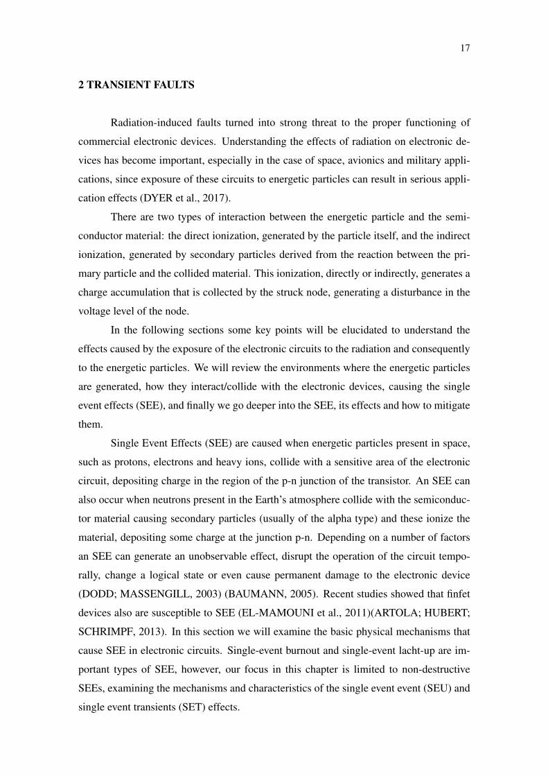
2.1 Single Event Effects - Physical mechanisms
There are two ways in which an energy particle can deposit charges in a semi-
conductor device: direct ionization by the particle itself, Figure 2.1a, and ionization by
secondary particles generated by the collision between the incident particle and the mate-
rial hit, Figure 2.1b. The two mechanisms can lead to the malfunction of a circuit due to
the charge collected by the struck device.
Figure 2.1: Charge collection mechanism for a SEE.
When a particle strikes a microelectronic device, the most sensitive regions are
usually reverse-biased p-n junctions, particularly if the junction is floating or weakly
driven (with only a small drive transistor or high resistance load sourcing the current
required to keep the node in its state) (BAUMANN, 2005). The high field present in a
reverse-biased junction depletion region can very efficiently collect the particle-induced
charge through drift processes, leading to a transient current at the junction contact.
Strikes near a depletion region can also result in significant transient currents as carri-
ers diffuse into the vicinity of the depletion region field where they can be efficiently
collected. Even for direct strikes, diffusion plays a role as carriers generated beyond the
depletion region can diffuse back toward the junction. (DODD; MASSENGILL, 2003)
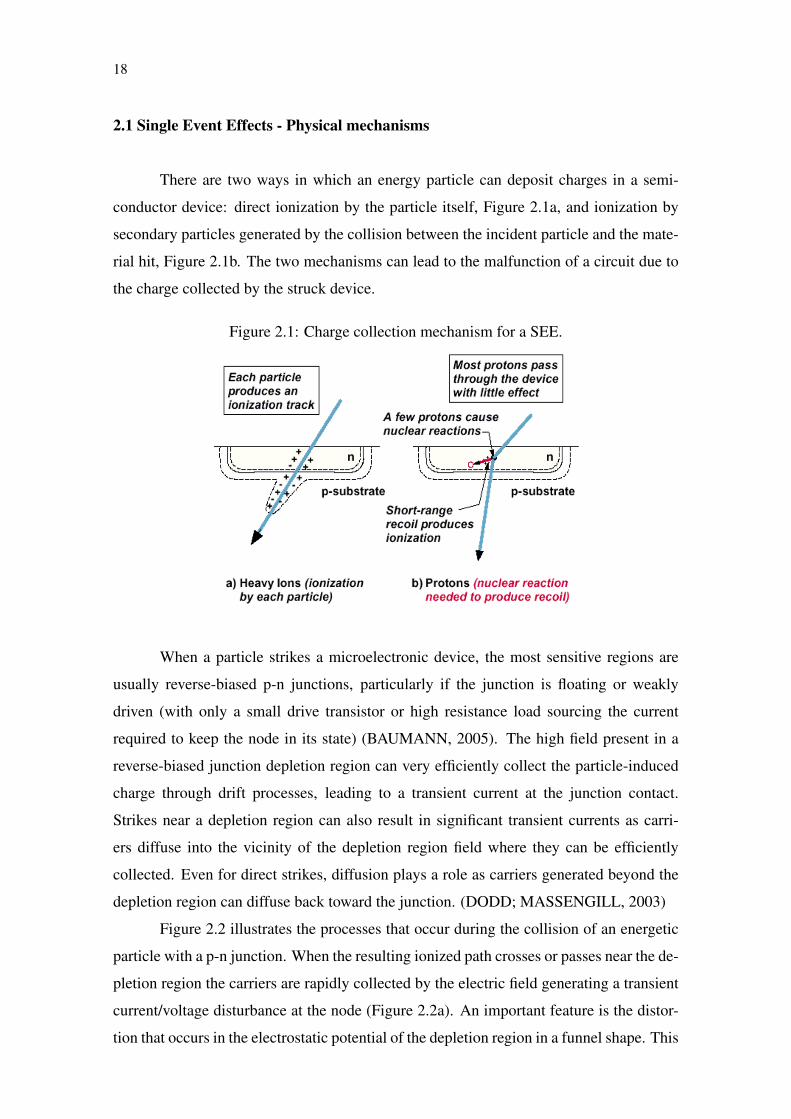
Figure 2.2 illustrates the processes that occur during the collision of an energetic
particle with a p-n junction. When the resulting ionized path crosses or passes near the de-
pletion region the carriers are rapidly collected by the electric field generating a transient
current/voltage disturbance at the node (Figure 2.2a). An important feature is the distor-
tion that occurs in the electrostatic potential of the depletion region in a funnel shape. This
19
funnel greatly enhances the efficiency of the drift collection by extending the high field
depletion region deeper into the substrate (Figure 2.2b). An extra charge is collected as
the electrons diffuse in the depletion region until all carriers are collected, recombined or
diffused away from the junction area (Figure 2.2c). The graph in Figure 2.2d elucidates
the difference in drift and diffusion collection, in the case of drift collection it occurs
within nanosecond, diffusion occurs in a longer time scale (hundreds of nanoseconds).
Figure 2.2: Charge generation and collection phases in a reverse-biased junction and theresultant current pulse caused by the passage of a high-energy ion. (BAUMANN, 2005)
2.2 Single Event Upset (SEU)
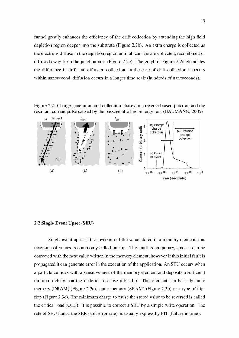
Single event upset is the inversion of the value stored in a memory element, this
inversion of values is commonly called bit-flip. This fault is temporary, since it can be
corrected with the next value written in the memory element, however if this initial fault is
propagated it can generate error in the execution of the application. An SEU occurs when
a particle collides with a sensitive area of the memory element and deposits a sufficient
minimum charge on the material to cause a bit-flip. This element can be a dynamic
memory (DRAM) (Figure 2.3a), static memory (SRAM) (Figure 2.3b) or a type of flip-
flop (Figure 2.3c). The minimum charge to cause the stored value to be reversed is called
the critical load (Qcrit). It is possible to correct a SEU by a simple write operation. The
rate of SEU faults, the SER (soft error rate), is usually express by FIT (failure in time).

20
Figure 2.3: Single event upset in different types of memory elements. (MUNTEANU;AUTRAN, 2008)
(a) DRAM. (b) SRAM.
(c) Flip-flop.
2.3 Single Event Transient (SET)
Single Event Transient (SET), is a voltage/current transient disturbance generated
when an energetic particle struck a sensible node in a combinational part of the integrated
circuit. With the constant miniaturization of the size of CMOS technology it has become
clear that SET has become a significant mechanism in error rates. The scaling of the tech-
nology came along with higher operating frequencies, lower supply voltages and smaller
noise margins, making the circuit sensitivity to SET higher.
Any node in the combinational circuit can be affected by a fault and generate
a transient disturbance in the current/voltage with sufficient duration to be propagated
along the combinational circuit until it is captured by a memory element. However only
a few transients are captured, the chance of a SET being captured involves three issues:
21
the probability of a functionally sensitive SET path between the node and the sequential
element; the rate at which the SET loses force at each logical level that it traverses until
it reaches the sequential element; and the chance of the generated transient pulse being
effectively captured and stored in the sequential element. These three questions lead to
three masking phenomena:
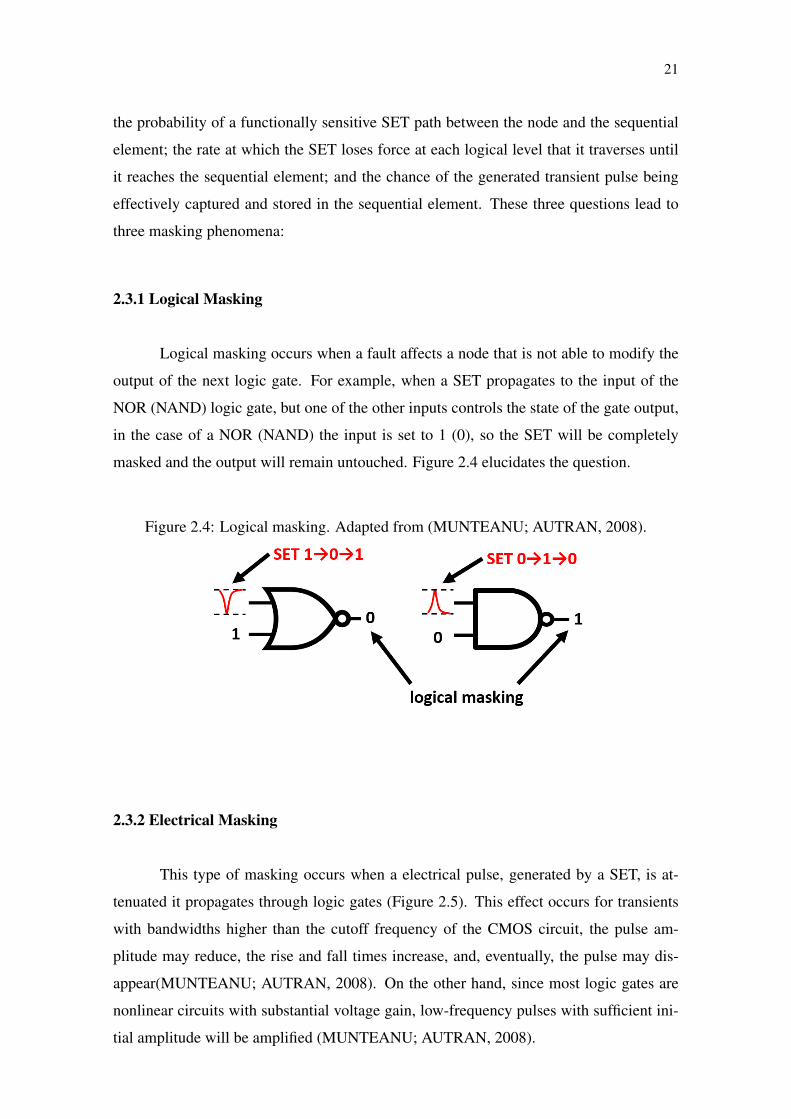
2.3.1 Logical Masking
Logical masking occurs when a fault affects a node that is not able to modify the
output of the next logic gate. For example, when a SET propagates to the input of the
NOR (NAND) logic gate, but one of the other inputs controls the state of the gate output,
in the case of a NOR (NAND) the input is set to 1 (0), so the SET will be completely
masked and the output will remain untouched. Figure 2.4 elucidates the question.
Figure 2.4: Logical masking. Adapted from (MUNTEANU; AUTRAN, 2008).
2.3.2 Electrical Masking
This type of masking occurs when a electrical pulse, generated by a SET, is at-
tenuated it propagates through logic gates (Figure 2.5). This effect occurs for transients
with bandwidths higher than the cutoff frequency of the CMOS circuit, the pulse am-
plitude may reduce, the rise and fall times increase, and, eventually, the pulse may dis-
appear(MUNTEANU; AUTRAN, 2008). On the other hand, since most logic gates are
nonlinear circuits with substantial voltage gain, low-frequency pulses with sufficient ini-
tial amplitude will be amplified (MUNTEANU; AUTRAN, 2008).
22
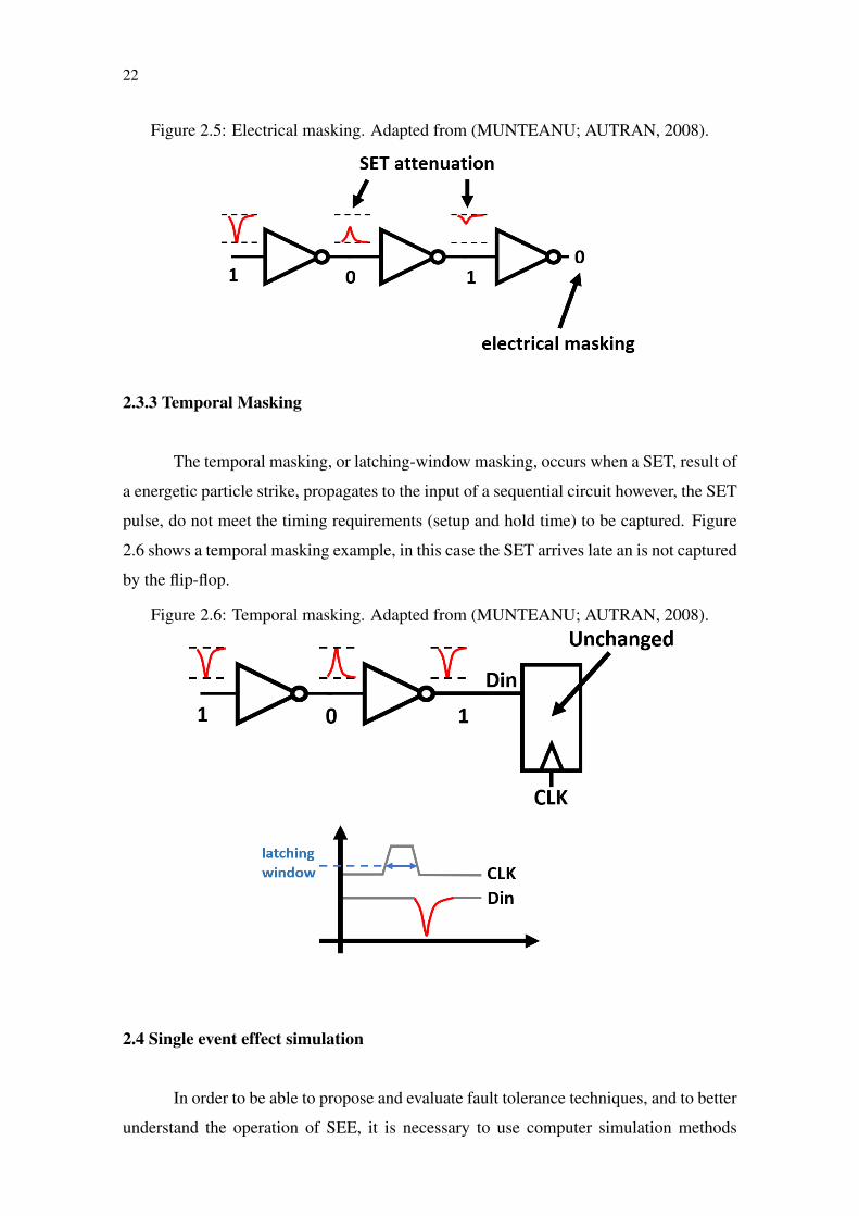
Figure 2.5: Electrical masking. Adapted from (MUNTEANU; AUTRAN, 2008).
2.3.3 Temporal Masking
The temporal masking, or latching-window masking, occurs when a SET, result of
a energetic particle strike, propagates to the input of a sequential circuit however, the SET
pulse, do not meet the timing requirements (setup and hold time) to be captured. Figure
2.6 shows a temporal masking example, in this case the SET arrives late an is not captured
by the flip-flop.
Figure 2.6: Temporal masking. Adapted from (MUNTEANU; AUTRAN, 2008).
2.4 Single event effect simulation
In order to be able to propose and evaluate fault tolerance techniques, and to better
understand the operation of SEE, it is necessary to use computer simulation methods

23
capable of modeling the mechanisms and effects of an energetic particle when it hit a
sensitive area of the electric circuit. We can divide the simulation methods according
to the abstraction of their mechanisms and the precision of their results: logical level
simulation, electrical level, full 3D numerical simulation and mixed-mode simulation.
2.4.1 Logic level simulation
The logic level simulation allows the functional analysis of the circuit evaluating
the nodes and the outputs when the same simulated application suffers with a SEU or
SET. At this level of abstraction the simulation is done through a behavioral description
in RTL (register transfer level), logic gates description or a transistor level description.
Hardware description languages (HDL), like VHDL and Verilog, are commonly used for
this type of simulation. It is also possible to simulate the delay time of the logic gates in
order to obtain a better simulation of the DUT (design under test).
In the logic level simulation a SET or SEU is modeled by forcing a logic value
(true, false or unknown) in a signal or node of the DUT, allowing also the definition of the
SEE pulse length. Figure 2.7 shows a DUT simulation where the SET is propagated and
is captured by the flip-flop.
Figure 2.7: Logic level simulation of a SET (MUNTEANU; AUTRAN, 2008)
2.4.2 Electric level simulation
Electric level simulation is done with software build to solve numerous equations
that describe the behavior of the circuit. The electrical behavior models, static or dynamic,
of many devices (transistor, resistor, capacitor and etc) are the basic components used by
the software to simulate the DUT. Usually the models are based on analytical formulas,
24
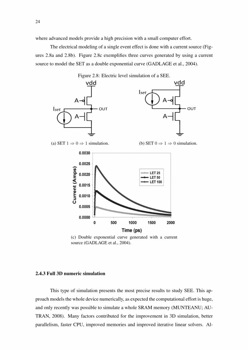
where advanced models provide a high precision with a small computer effort.
The electrical modeling of a single event effect is done with a current source (Fig-
ures 2.8a and 2.8b). Figure 2.8c exemplifies three curves generated by using a current
source to model the SET as a double exponential curve (GADLAGE et al., 2004).
Figure 2.8: Electric level simulation of a SEE.
(a) SET 1⇒ 0⇒ 1 simulation. (b) SET 0⇒ 1⇒ 0 simulation.
(c) Double exponential curve generated with a currentsource (GADLAGE et al., 2004).
2.4.3 Full 3D numeric simulation
This type of simulation presents the most precise results to study SEE. This ap-
proach models the whole device numerically, as expected the computational effort is huge,
and only recently was possible to simulate a whole SRAM memory (MUNTEANU; AU-
TRAN, 2008). Many factors contributed for the improvement in 3D simulation, better
parallelism, faster CPU, improved memories and improved iterative linear solvers. Al-

25
Figure 2.9: SRAM cell 3D simulation. (MUNTEANU; AUTRAN, 2008)
though the simulation time needed for simulation of the entire cell in the 3-D device
domain was substantially reduced, it is still considerable compared with the time needed
to simulate the same circuit with Spice and mixed-level approaches. The emergence of
PC-based parallel machines (clusters) with hundreds of processors and important mem-
ory resource is certainly one very promising way to develop in the future such full 3-D
simulations on portions of circuits (MUNTEANU; AUTRAN, 2008).
2.4.4 Mixed-mode simulation
The limitations of circuit level simulation can be overcome by using physically-
based device simulation to predict the response to ionizing radiation of the struck de-
vice. This approach is referred to as “mixed-mode” or “mixed-level” simulation, since
the struck device is described by simulation in the device domain and the other devices
by compact models. The two simulation domains are tied together by the boundary con-
ditions at contacts, and the solution to both sets of equations is rolled into a single matrix
solution. Figure 2.10a shows the construction of an SRAM cell in the frame of mixed-
mode simulation. Only the struck transistor is modeled in the 3-D device domain. Figure
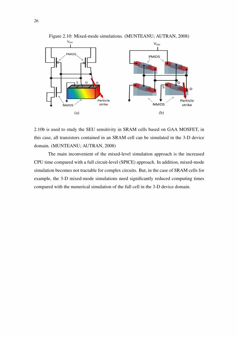
26
Figure 2.10: Mixed-mode simulations. (MUNTEANU; AUTRAN, 2008)
(a) (b)
2.10b is used to study the SEU sensitivity in SRAM cells based on GAA MOSFET, in
this case, all transistors contained in an SRAM cell can be simulated in the 3-D device
domain. (MUNTEANU; AUTRAN, 2008)
The main inconvenient of the mixed-level simulation approach is the increased
CPU time compared with a full circuit-level (SPICE) approach. In addition, mixed-mode
simulation becomes not tractable for complex circuits. But, in the case of SRAM cells for
example, the 3-D mixed-mode simulations need significantly reduced computing times
compared with the numerical simulation of the full cell in the 3-D device domain.
27
3 TMR AND APPROXIMATE CIRCUITS
Hardware redundancy is often used to mitigate SET, because SET can be detected
and masked by voting. Within this approach, Triple Modular Redundancy (TMR) is a
well-known redundancy technique, which provides very good concurrent correction ca-
pabilities. However, these techniques introduce very large cost in terms of both area and
power consumption, greater than 200% in area. Alternatively, partial redundancy is often
sought in order to find a good balance between the reliability requirements and the area,
power and performance requirements (POLIAN; HAYES, 2010).
Within this context, approximated circuits have recently emerged as an alternative
approach for building partial TMR solutions. An approximate logic circuit is a circuit
that performs a different but closely related logic function to the original circuit. As it is
not required to exactly match the original circuit, the approximate circuit can be smaller,
faster and have lower power consumption but it can still be used to detect or correct errors
where it matches with the original circuit.
Approximate logic circuits can be used in the TMR instead of exact copies of the
original design, and the designer can select the level of approximation. A closer approxi-
mation provides higher fault tolerance but also increases the area and power. In contrast,
this continuous trade-off is not possible when exact TMR is used. However, generation
of optimal approximate circuits for any given application is a challenging problem.
This chapter is organized as follows. Section 3.1 introduces the concept of spatial
redundancy through N-tuple Modular Redundancy (NMR) techniques. Section 3.2 eluci-
dates some basic information about the aproximate circuits technique. Finally, in Section
3.3, the latest approaches for the creating of approximated circuits are presented.
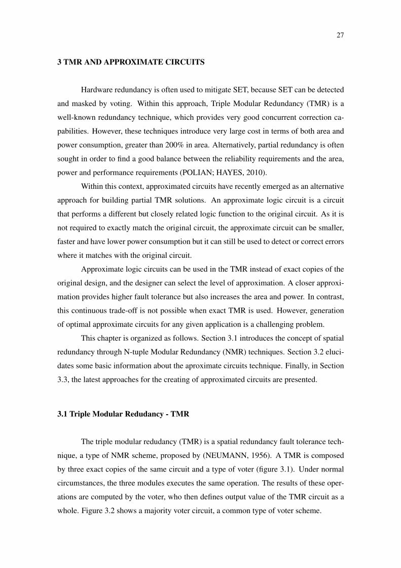
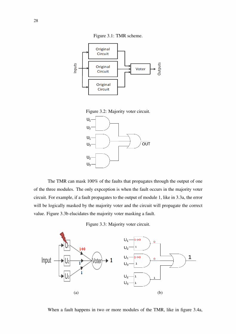
3.1 Triple Modular Redudancy - TMR
The triple modular redudancy (TMR) is a spatial redundancy fault tolerance tech-
nique, a type of NMR scheme, proposed by (NEUMANN, 1956). A TMR is composed
by three exact copies of the same circuit and a type of voter (figure 3.1). Under normal
circumstances, the three modules executes the same operation. The results of these oper-
ations are computed by the voter, who then defines output value of the TMR circuit as a
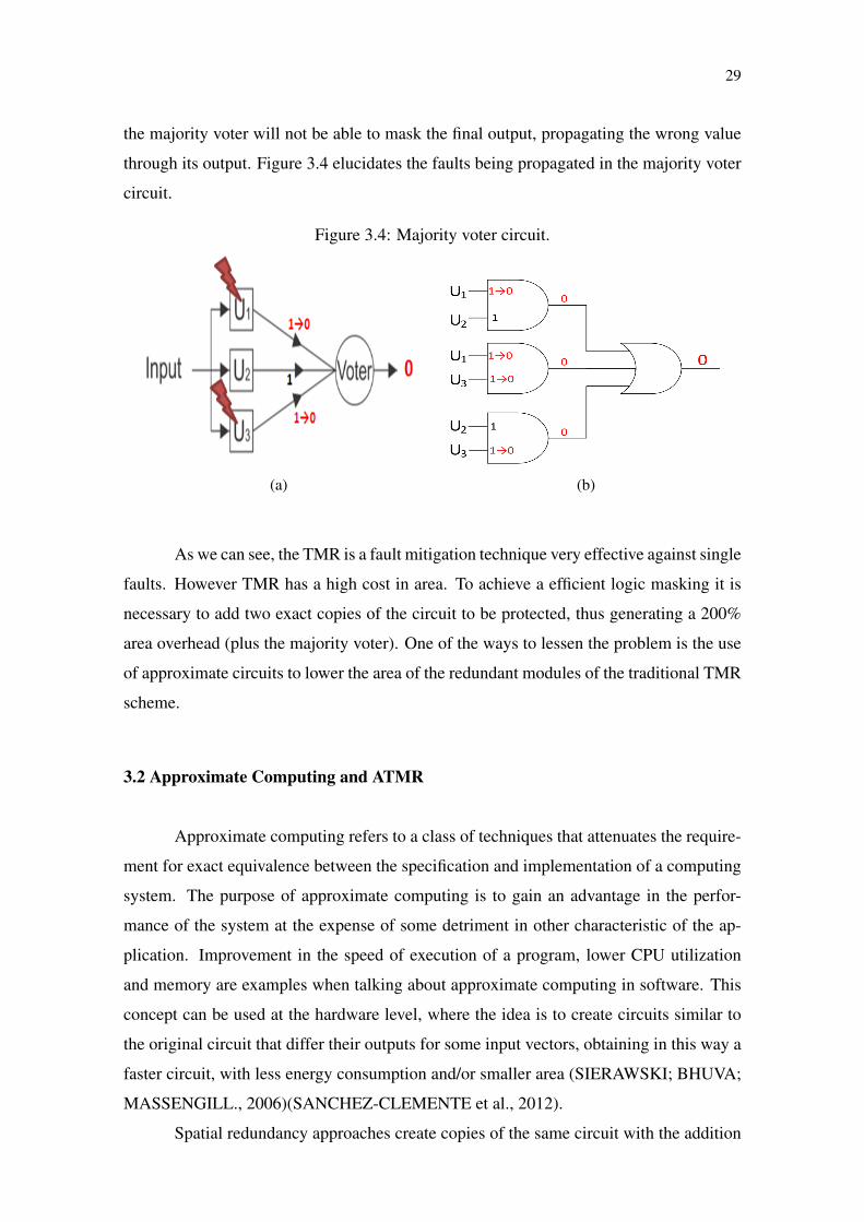
whole. Figure 3.2 shows a majority voter circuit, a common type of voter scheme.
28
Figure 3.1: TMR scheme.
Figure 3.2: Majority voter circuit.
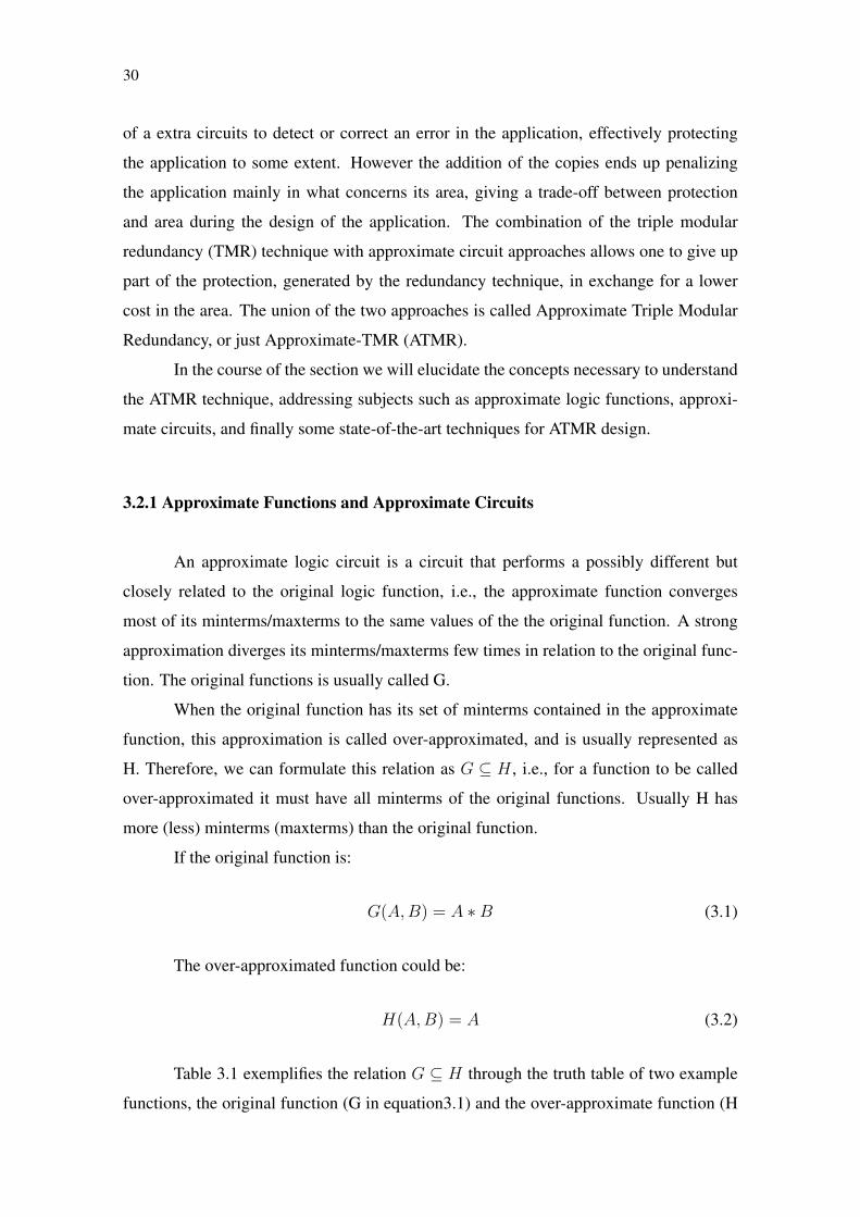
The TMR can mask 100% of the faults that propagates through the output of one
of the three modules. The only expception is when the fault occurs in the majority voter
circuit. For example, if a fault propagates to the output of module 1, like in 3.3a, the error
will be logically masked by the majority voter and the circuit will propagate the correct
value. Figure 3.3b elucidates the majority voter masking a fault.
Figure 3.3: Majority voter circuit.
(a) (b)
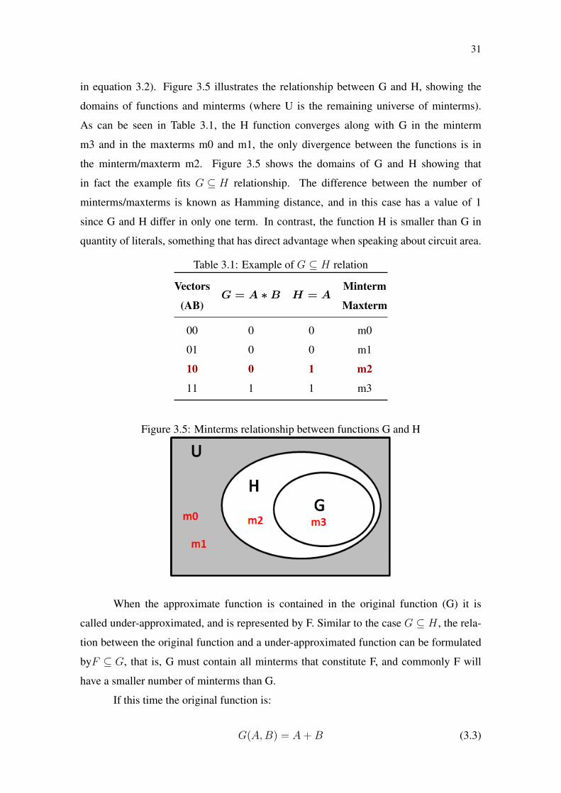
When a fault happens in two or more modules of the TMR, like in figure 3.4a,
29
the majority voter will not be able to mask the final output, propagating the wrong value
through its output. Figure 3.4 elucidates the faults being propagated in the majority voter
circuit.
Figure 3.4: Majority voter circuit.
(a) (b)
As we can see, the TMR is a fault mitigation technique very effective against single
faults. However TMR has a high cost in area. To achieve a efficient logic masking it is
necessary to add two exact copies of the circuit to be protected, thus generating a 200%
area overhead (plus the majority voter). One of the ways to lessen the problem is the use
of approximate circuits to lower the area of the redundant modules of the traditional TMR
scheme.
3.2 Approximate Computing and ATMR
Approximate computing refers to a class of techniques that attenuates the require-
ment for exact equivalence between the specification and implementation of a computing
system. The purpose of approximate computing is to gain an advantage in the perfor-
mance of the system at the expense of some detriment in other characteristic of the ap-
plication. Improvement in the speed of execution of a program, lower CPU utilization
and memory are examples when talking about approximate computing in software. This
concept can be used at the hardware level, where the idea is to create circuits similar to
the original circuit that differ their outputs for some input vectors, obtaining in this way a
faster circuit, with less energy consumption and/or smaller area (SIERAWSKI; BHUVA;
MASSENGILL., 2006)(SANCHEZ-CLEMENTE et al., 2012).
Spatial redundancy approaches create copies of the same circuit with the addition
30
of a extra circuits to detect or correct an error in the application, effectively protecting
the application to some extent. However the addition of the copies ends up penalizing
the application mainly in what concerns its area, giving a trade-off between protection
and area during the design of the application. The combination of the triple modular
redundancy (TMR) technique with approximate circuit approaches allows one to give up
part of the protection, generated by the redundancy technique, in exchange for a lower
cost in the area. The union of the two approaches is called Approximate Triple Modular
Redundancy, or just Approximate-TMR (ATMR).
In the course of the section we will elucidate the concepts necessary to understand
the ATMR technique, addressing subjects such as approximate logic functions, approxi-
mate circuits, and finally some state-of-the-art techniques for ATMR design.
3.2.1 Approximate Functions and Approximate Circuits
An approximate logic circuit is a circuit that performs a possibly different but
closely related to the original logic function, i.e., the approximate function converges
most of its minterms/maxterms to the same values of the the original function. A strong
approximation diverges its minterms/maxterms few times in relation to the original func-
tion. The original functions is usually called G.
When the original function has its set of minterms contained in the approximate
function, this approximation is called over-approximated, and is usually represented as
H. Therefore, we can formulate this relation as G ⊆ H , i.e., for a function to be called
over-approximated it must have all minterms of the original functions. Usually H has
more (less) minterms (maxterms) than the original function.
If the original function is:
G(A,B) = A ∗B (3.1)
The over-approximated function could be:
H(A,B) = A (3.2)
Table 3.1 exemplifies the relation G ⊆ H through the truth table of two example
functions, the original function (G in equation3.1) and the over-approximate function (H
31
in equation 3.2). Figure 3.5 illustrates the relationship between G and H, showing the
domains of functions and minterms (where U is the remaining universe of minterms).
As can be seen in Table 3.1, the H function converges along with G in the minterm
m3 and in the maxterms m0 and m1, the only divergence between the functions is in
the minterm/maxterm m2. Figure 3.5 shows the domains of G and H showing that
in fact the example fits G ⊆ H relationship. The difference between the number of
minterms/maxterms is known as Hamming distance, and in this case has a value of 1
since G and H differ in only one term. In contrast, the function H is smaller than G in
quantity of literals, something that has direct advantage when speaking about circuit area.
Table 3.1: Example of G ⊆ H relation
Vectors
(AB)G = A ∗B H = A
Minterm
Maxterm
00 0 0 m0
01 0 0 m1
10 0 1 m2
11 1 1 m3
Figure 3.5: Minterms relationship between functions G and H
When the approximate function is contained in the original function (G) it is
called under-approximated, and is represented by F. Similar to the case G ⊆ H , the rela-
tion between the original function and a under-approximated function can be formulated
byF ⊆ G, that is, G must contain all minterms that constitute F, and commonly F will
have a smaller number of minterms than G.
If this time the original function is:
G(A,B) = A + B (3.3)

32
The under-approximated function could be:
F (A,B) = A (3.4)
Table 3.2 exemplifies the relation F ⊆ G through the truth table of two example
functions, the original (G) and the over-approximate function (F). Figure 3.6 shows the
relationship between G and H showing the domain of the functions and the minterms
(where U is the remaining universe of minterms). As can be seen in Table 3.2 the func-
tion F converges along with G in minterms m2 and m3 and in maxterm m0. The only
divergence between functions is in minterm/maxterm m1. Figure 3.6 shows the domains
of G and F showing that in fact the example fits F ⊆ G relationship. The Hamming dis-
tance in this case has a value of 1 since G and F differ in only one term. In contrast, the
F function is smaller than G in number of literals, which has direct advantage when it
comes to circuit area.
Table 3.2: Example of F ⊆ G relation
Vectors
(AB)G = A + B F = A
Minterm
Maxterm
00 0 0 m0
01 1 0 m1
10 1 1 m2
11 1 1 m3
Figure 3.6: Minterms relationship between functions G and F
Through previous cases it was possible to understand and visualize what the ap-
proximate functions are, and how they can be classified. However we derived only one
function from each type in each of the previous examples. The purpose of the previous
33
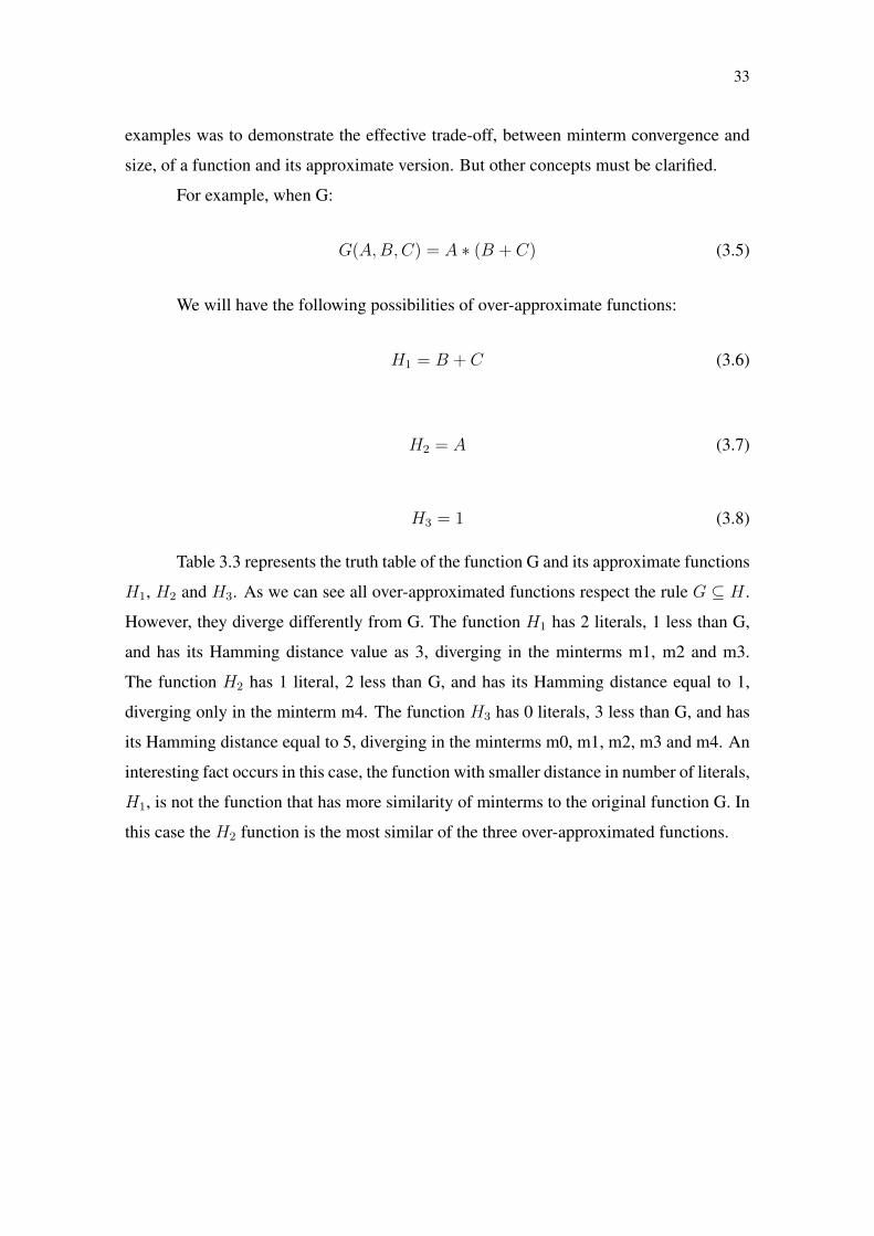
examples was to demonstrate the effective trade-off, between minterm convergence and
size, of a function and its approximate version. But other concepts must be clarified.
For example, when G:
G(A,B,C) = A ∗ (B + C) (3.5)
We will have the following possibilities of over-approximate functions:
H1 = B + C (3.6)
H2 = A (3.7)
H3 = 1 (3.8)
Table 3.3 represents the truth table of the function G and its approximate functions
H1, H2 and H3. As we can see all over-approximated functions respect the rule G ⊆ H .
However, they diverge differently from G. The function H1 has 2 literals, 1 less than G,
and has its Hamming distance value as 3, diverging in the minterms m1, m2 and m3.
The function H2 has 1 literal, 2 less than G, and has its Hamming distance equal to 1,
diverging only in the minterm m4. The function H3 has 0 literals, 3 less than G, and has
its Hamming distance equal to 5, diverging in the minterms m0, m1, m2, m3 and m4. An
interesting fact occurs in this case, the function with smaller distance in number of literals,
H1, is not the function that has more similarity of minterms to the original function G. In
this case the H2 function is the most similar of the three over-approximated functions.

34
Table 3.3: Truth table of G and its over-approximated functions (H1, H2 and H3)
Vectors
(ABC)G H1 H2 H3
Minterm
Maxterm
000 0 0 0 1 m0
001 0 1 0 1 m1
010 0 1 0 1 m2
011 0 1 0 1 m3
100 0 0 1 1 m4
101 1 1 1 1 m5
110 1 1 1 1 m6
111 1 1 1 1 m7
The same questions can be asked about the under-approximated functions. Again
G is:
G(A,B,C) = A ∗ (B + C) (3.9)
We will have the following possibilities of under-approximate functions:
F1 = A ∗B (3.10)
F2 = A ∗ C (3.11)
F3 = 0 (3.12)
Table 3.4 represents the truth table of the G function and its under-approximate
functions F1, F2 and F3. As we can see all functions F respect the rule F ⊆ G rule that
define them as under-approximate functions. However, each of the F functions diverge
differently from the G function. Both the F1 function and the F2 function have 2 literals,
1 less than G, and both have their Hamming distance by 1, however they diverge from G
in minterms differently, F1 diverges in minterm m5 and F2 in minterm m6. The function
F3 has 0 literals, 3 less than G, and has its Hamming distance equal to 3, diverging at the
minterms m5, m6, and m7.
35
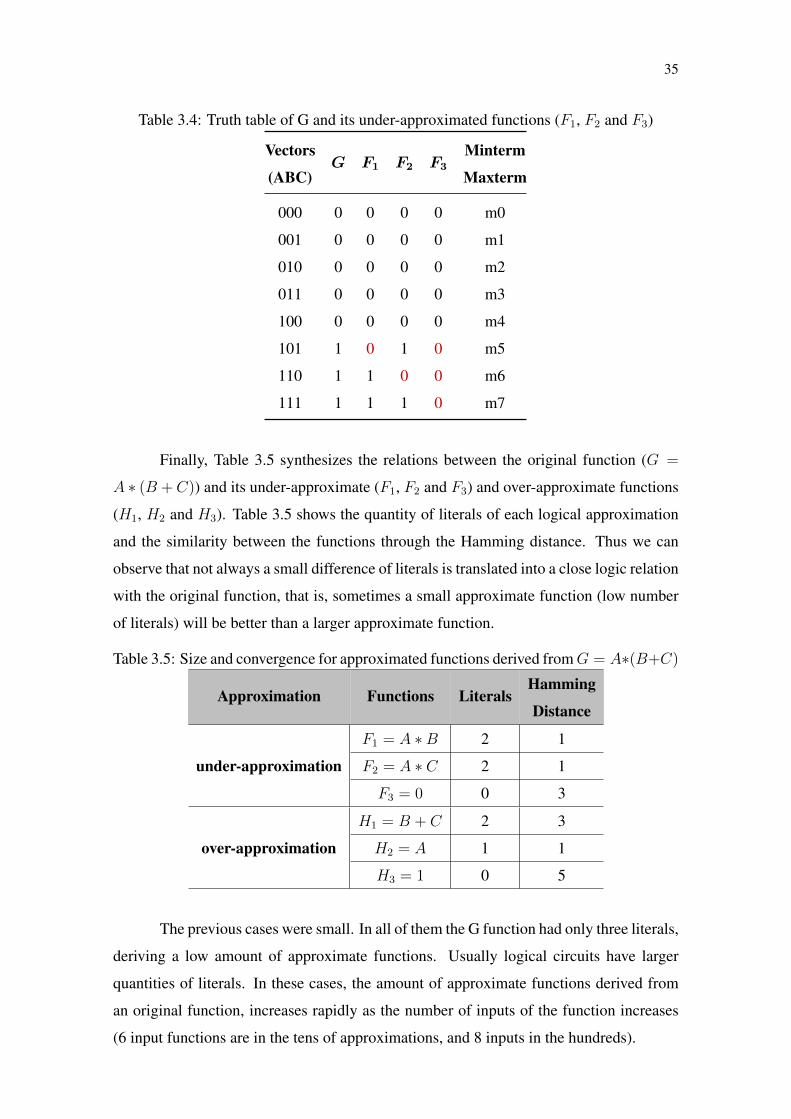
Table 3.4: Truth table of G and its under-approximated functions (F1, F2 and F3)
Vectors
(ABC)G F1 F2 F3
Minterm
Maxterm
000 0 0 0 0 m0
001 0 0 0 0 m1
010 0 0 0 0 m2
011 0 0 0 0 m3
100 0 0 0 0 m4
101 1 0 1 0 m5
110 1 1 0 0 m6
111 1 1 1 0 m7
Finally, Table 3.5 synthesizes the relations between the original function (G =
A ∗ (B + C)) and its under-approximate (F1, F2 and F3) and over-approximate functions
(H1, H2 and H3). Table 3.5 shows the quantity of literals of each logical approximation
and the similarity between the functions through the Hamming distance. Thus we can
observe that not always a small difference of literals is translated into a close logic relation
with the original function, that is, sometimes a small approximate function (low number
of literals) will be better than a larger approximate function.
Table 3.5: Size and convergence for approximated functions derived from G = A∗(B+C)
Approximation Functions LiteralsHamming
Distance
F1 = A ∗B 2 1
F2 = A ∗ C 2 1under-approximation
F3 = 0 0 3
H1 = B + C 2 3
H2 = A 1 1over-approximation
H3 = 1 0 5
The previous cases were small. In all of them the G function had only three literals,
deriving a low amount of approximate functions. Usually logical circuits have larger
quantities of literals. In these cases, the amount of approximate functions derived from
an original function, increases rapidly as the number of inputs of the function increases
(6 input functions are in the tens of approximations, and 8 inputs in the hundreds).
36
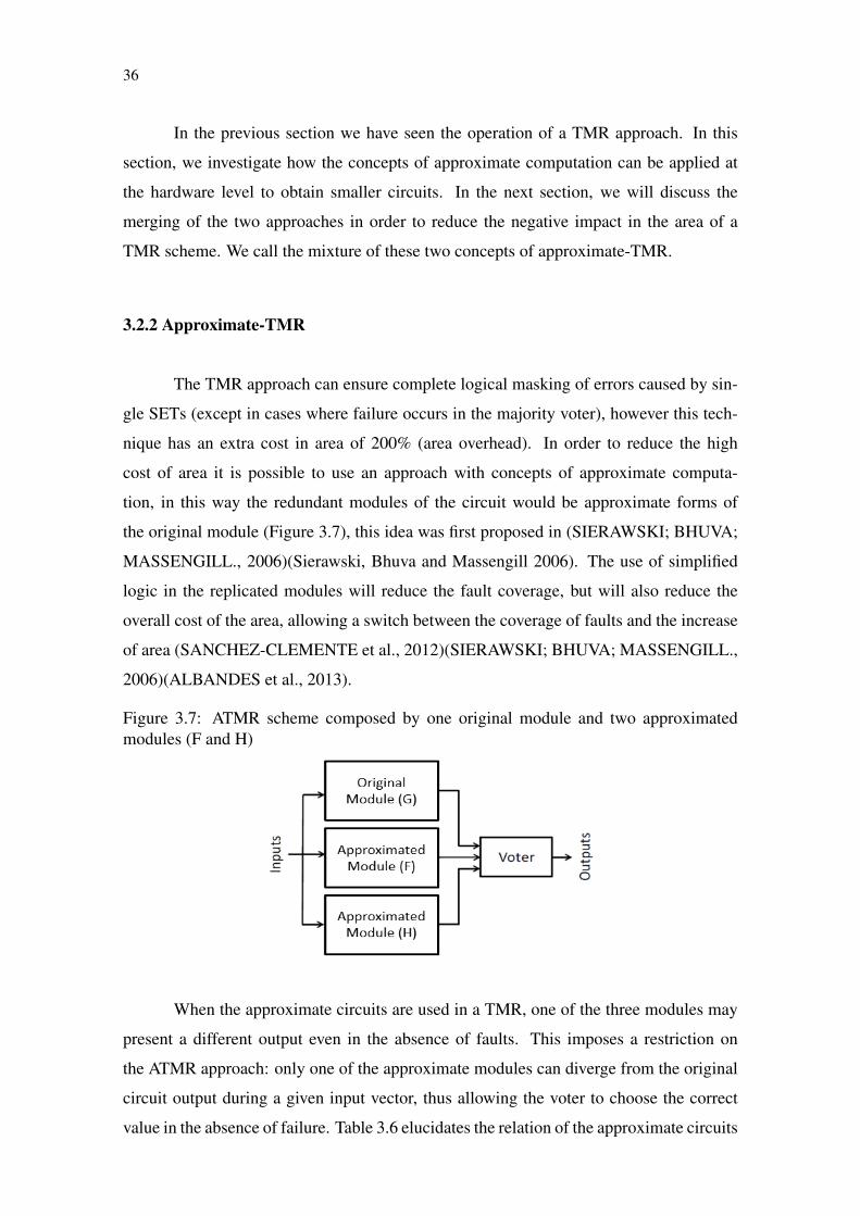
In the previous section we have seen the operation of a TMR approach. In this
section, we investigate how the concepts of approximate computation can be applied at
the hardware level to obtain smaller circuits. In the next section, we will discuss the
merging of the two approaches in order to reduce the negative impact in the area of a
TMR scheme. We call the mixture of these two concepts of approximate-TMR.
3.2.2 Approximate-TMR
The TMR approach can ensure complete logical masking of errors caused by sin-
gle SETs (except in cases where failure occurs in the majority voter), however this tech-
nique has an extra cost in area of 200% (area overhead). In order to reduce the high
cost of area it is possible to use an approach with concepts of approximate computa-
tion, in this way the redundant modules of the circuit would be approximate forms of
the original module (Figure 3.7), this idea was first proposed in (SIERAWSKI; BHUVA;
MASSENGILL., 2006)(Sierawski, Bhuva and Massengill 2006). The use of simplified
logic in the replicated modules will reduce the fault coverage, but will also reduce the
overall cost of the area, allowing a switch between the coverage of faults and the increase
of area (SANCHEZ-CLEMENTE et al., 2012)(SIERAWSKI; BHUVA; MASSENGILL.,
2006)(ALBANDES et al., 2013).
Figure 3.7: ATMR scheme composed by one original module and two approximatedmodules (F and H)
When the approximate circuits are used in a TMR, one of the three modules may
present a different output even in the absence of faults. This imposes a restriction on
the ATMR approach: only one of the approximate modules can diverge from the original
circuit output during a given input vector, thus allowing the voter to choose the correct
value in the absence of failure. Table 3.6 elucidates the relation of the approximate circuits

37
and the original in an ATMR scheme, demonstrating that in the absence of failures the
voter would continue to generate the correct results.
Table 3.6: Truth table for a ATMR schemeVectors(ABC) G = A ∗ (B + C) F = A ∗B H = A
VoterOutput
FunctionsRelations
000 0 0 0 0 G = F = H001 0 0 0 0 G = F = H010 0 0 0 0 G = F = H011 0 0 0 0 G = F = H100 0 0 1 0 G = F 6= H101 1 0 1 1 G = H 6= F110 1 1 1 1 G = F = H111 1 1 1 1 G = F = H
For an ATMR scheme to work correctly, i.e., for its voter to indicate the correct
value in the absence of failure, it is necessary to follow the following rule: F ⊆ G ⊆ H
(illustrated in Figure 3.8), that is, every minterm of F must be a minterm of G , and every
minterm of G must be a minterm of H. This rule assures that H will only evaluate at 0
when G evaluates to 0, and that F will only get its output at 1 when G has its output at 1.
Looking again at Table 3.6 we can see that three different relations are created between
the functions by F ⊆ G ⊆ H constraint:
• G = F = H , where the approach works like a traditional TMR with the three
modules converging to the same value
• G = F 6= H , when G and F converge to 0 but H evaluates to 1
• G = H 6= F when G and H converge to 0 but F evaluates to 0
It is important to emphasize that the rule F ⊆ G ⊆ H is to prevent cases where
both approximate modules (F and H) will diverge simultaneously from the original mod-
ule in case G 6= F = H . Another fact is that an ATMR can be composed of two original
modules and one approximated or even be composed only by approximated modules (AL-
BANDES et al., 2015a), we will talk about the latter in future chapters.
Figure 3.8: Illustration of the F ⊆ G ⊆ H relation. Gray area represent the G = F = Hstate. White are shows the G = F 6= H and G = H 6= F states.

38
The previous analysis, in order to elucidate an initial concept of relationship be-
tween the original function and its approximate functions, was done under the condition
that there is no fault in the ATMR. However the objective of an ATMR is the mitiga-
tion of faults, so it is necessary to analyze the adverse behavior. Assuming the following
configuration of an ATMR:
Original function:
G = A ∗ (B + C) (3.13)
Under-approximated module:
F = A ∗B (3.14)
Over-approximated module:
H = A (3.15)
3.2.2.1 Case 1: Fault during G = F = H state
The first example (Table 3.7) simulates a fault in the under-approximated circuit
(F) of the ATMR when the input vector is in 000. In this situation the relation between
the functions is G = F = H. Even with the change in the relation between the modules the
voter keeps the correct value at its output, masking the error. Whenever the relationship
between functions initially is G = F = H the ATMR will behave like a traditional TMR,
guaranteeing 100% logical masking against single transient faults propagated at the output
of one of the modules.
Table 3.7: Truth table of a ATMR scheme. Fault in one of the modules while in a protectedvectors.
Vectors(ABC) G = A*(B+C) F=A*B H=A Voter
OutputFunctionsRelations
000 0 1⇒ 0 0 0 G = F 6= H ⇒ G = F = H001 0 0 0 0 G = F = H010 0 0 0 0 G = F = H011 0 0 0 0 G = F = H100 0 0 1 0 G = F 6= H101 1 0 1 1 G = H 6= F110 1 1 1 1 G = F = H111 1 1 1 1 G = F = H
39
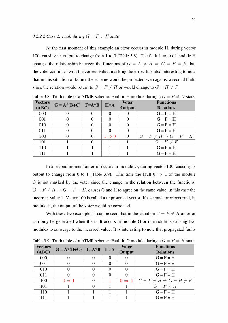
3.2.2.2 Case 2: Fault during G = F 6= H state
At the first moment of this example an error occurs in module H, during vector
100, causing its output to change from 1 to 0 (Table 3.8). The fault 1 ⇒ 0 of module H
changes the relationship between the functions of G = F 6= H ⇒ G = F = H , but
the voter continues with the correct value, masking the error. It is also interesting to note
that in this situation of failure the scheme would be protected even against a second fault,
since the relation would return to G = F 6= H or would change to G = H 6= F .
Table 3.8: Truth table of a ATMR scheme. Fault in H module during a G = F 6= H state.Vectors(ABC) G = A*(B+C) F=A*B H=A Voter
OutputFunctionsRelations
000 0 0 0 0 G = F = H001 0 0 0 0 G = F = H010 0 0 0 0 G = F = H011 0 0 0 0 G = F = H100 0 0 1⇒ 0 0 G = F 6= H ⇒ G = F = H101 1 0 1 1 G = H 6= F110 1 1 1 1 G = F = H111 1 1 1 1 G = F = H
In a second moment an error occurs in module G, during vector 100, causing its
output to change from 0 to 1 (Table 3.9). This time the fault 0 ⇒ 1 of the module
G is not masked by the voter since the change in the relation between the functions,
G = F 6= H ⇒ G = F = H , causes G and H to agree on the same value, in this case the
incorrect value 1. Vector 100 is called a unprotected vector. If a second error occurred, in
module H, the output of the voter would be corrected.
With these two examples it can be seen that in the situation G = F 6= H an error
can only be generated when the fault occurs in module G or in module F, causing two
modules to converge to the incorrect value. It is interesting to note that propagated faults
Table 3.9: Truth table of a ATMR scheme. Fault in G module during a G = F 6= H state.Vectors(ABC) G = A*(B+C) F=A*B H=A Voter
OutputFunctionsRelations
000 0 0 0 0 G = F = H001 0 0 0 0 G = F = H010 0 0 0 0 G = F = H011 0 0 0 0 G = F = H100 0⇒ 1 0 1 0⇒ 1 G = F 6= H ⇒ G = H 6= F101 1 0 1 1 G = F 6= H110 1 1 1 1 G = F = H111 1 1 1 1 G = F = H
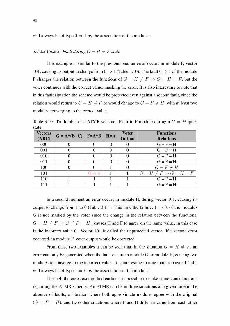
40
will always be of type 0⇒ 1 by the association of the modules.
3.2.2.3 Case 2: Fault during G = H 6= F state
This example is similar to the previous one, an error occurs in module F, vector
101, causing its output to change from 0⇒ 1 (Table 3.10). The fault 0⇒ 1 of the module
F changes the relation between the functions of G = H 6= F ⇒ G = H = F , but the
voter continues with the correct value, masking the error. It is also interesting to note that
in this fault situation the scheme would be protected even against a second fault, since the
relation would return to G = H 6= F or would change to G = F 6= H , with at least two
modules converging to the correct value.
Table 3.10: Truth table of a ATMR scheme. Fault in F module during a G = H 6= Fstate.
Vectors(ABC) G = A*(B+C) F=A*B H=A Voter
OutputFunctionsRelations
000 0 0 0 0 G = F = H001 0 0 0 0 G = F = H010 0 0 0 0 G = F = H011 0 0 0 0 G = F = H100 0 0 1 0 G = F 6= H101 1 0⇒ 1 1 1 G = H 6= F ⇒ G = H = F110 1 1 1 1 G = F = H111 1 1 1 1 G = F = H
In a second moment an error occurs in module H, during vector 101, causing its
output to change from 1 to 0 (Table 3.11). This time the failure, 1 ⇒ 0, of the modulus
G is not masked by the voter since the change in the relation between the functions,
G = H 6= F ⇒ G 6= F = H , causes H and F to agree on the same value, in this case
is the incorrect value 0. Vector 101 is called the unprotected vector. If a second error
occurred, in module F, voter output would be corrected.
From these two examples it can be seen that, in the situation G = H 6= F , an
error can only be generated when the fault occurs in module G or module H, causing two
modules to converge to the incorrect value. It is interesting to note that propagated faults
will always be of type 1⇒ 0 by the association of the modules.
Through the cases exemplified earlier it is possible to make some considerations
regarding the ATMR scheme. An ATMR can be in three situations at a given time in the
absence of faults, a situation where both approximate modules agree with the original
(G = F = H), and two other situations where F and H differ in value from each other

41
Table 3.11: Truth table of a ATMR scheme. Fault in H module during a G = F 6= Hstate.
Vectors(ABC) G = A*(B+C) F=A*B H=A Voter
OutputFunctionsRelations
000 0 0 0 0 G = F = H001 0 0 0 0 G = F = H010 0 0 0 0 G = F = H011 0 0 0 0 G = F = H100 0 0 1 0 G = F 6= H101 1 0 1⇒ 0 1⇒ 0 G = H 6= F ⇒ G 6= F = H110 1 1 1 1 G = F = H111 1 1 1 1 G = F = H
(G = F 6= H or G = H 6= F ). Approximate modules converge to the same value as the
original module, when the input vector (minterm) is in the gray area of Figure 3.9, in this
situation the ATMR scheme will be protected against single faults.
When the input vector is in the white area of Figure 3.9 the approximate modules
(F and H) will be in divergence (H 6= F ), and the ATMR will not be 100% protected
against single faults. In this situation, of divergence between F and H, the output of the
voter be defined by the original module. Errors in G are not masked when the scheme
state is in H 6= F , but if the error occurs in F or H it may be masked. Errors in module F
will be masked whenever H evaluates its output to 1. Errors in H will be masked whenever
F evaluates its output to 0.
Figure 3.9: Vectors, minterms and maxterms analysis

42
3.3 State-of-the-art
Several techniques for approximate circuit generation already exist in the litera-
ture. They range from BDD manipulation (CHOUDHURY; MOHANRAM, 2013), cube
selection (XIE et al., 2014), testability driven and stuck-at approaches (SANCHEZ-CLEMENTE
et al., 2012)(SANCHEZ-CLEMENTE; ENTRENA; GARCíA-VALDERAS, 2014) and
genetic algorithms (SANCHEZ-CLEMENTE et al., 2016). In our previous work we used
a boolean factoring algorithm to compute the approximate functions and structural re-
order techniques are applied to the circuits to improve the fault masking of the ATMR
(ALBANDES; KASTENSMIDT, 2014)(ALBANDES et al., 2015b)(ALBANDES et al.,
2015a).
When generating approximations of a target design, two major questions arise: 1)
how are approximate circuits designed? and 2) which are the requirements of the target
application to be satisfied? For the second question, several constraints in terms of area
overhead, power consumption, delay, reliability and different error metrics can be used,
depending on the particular requirements of each application. With respect to the first
question, several approaches can be followed. Although it is possible to manually gener-
ate approximations for a given design, thus having full control of the characteristics of ap-
proximations, the limited applicability of this approach renders it less interesting than the
automated generation of approximate circuits. When opting to implement an automated
design method, the previous questions can be reformulated as: 1) which mechanism is
applied to generate approximations? and 2) which criteria are used to selectively apply
this mechanism? Each one of the different existing techniques propose its own answer to
these questions.
3.3.1 ATMR Design: Stuck-at-Fault Approximation
In the fault approximation approach, approximate circuits are generated by assign-
ing logic constants to some circuit lines, which it is equivalent to forcing stuck-at faults.
In principle, any stuck-at fault could be forced to generate an approximation. However,
certain properties must be met in order to generate valid approximations for an ATMR.
In particular, the unate property is used to generate unidirectional approximations.
A logic function G is said to be positive on x if x only appears uncomplemented when G
is expressed as a sum of products. Alternatively, if x only appears complemented, then G
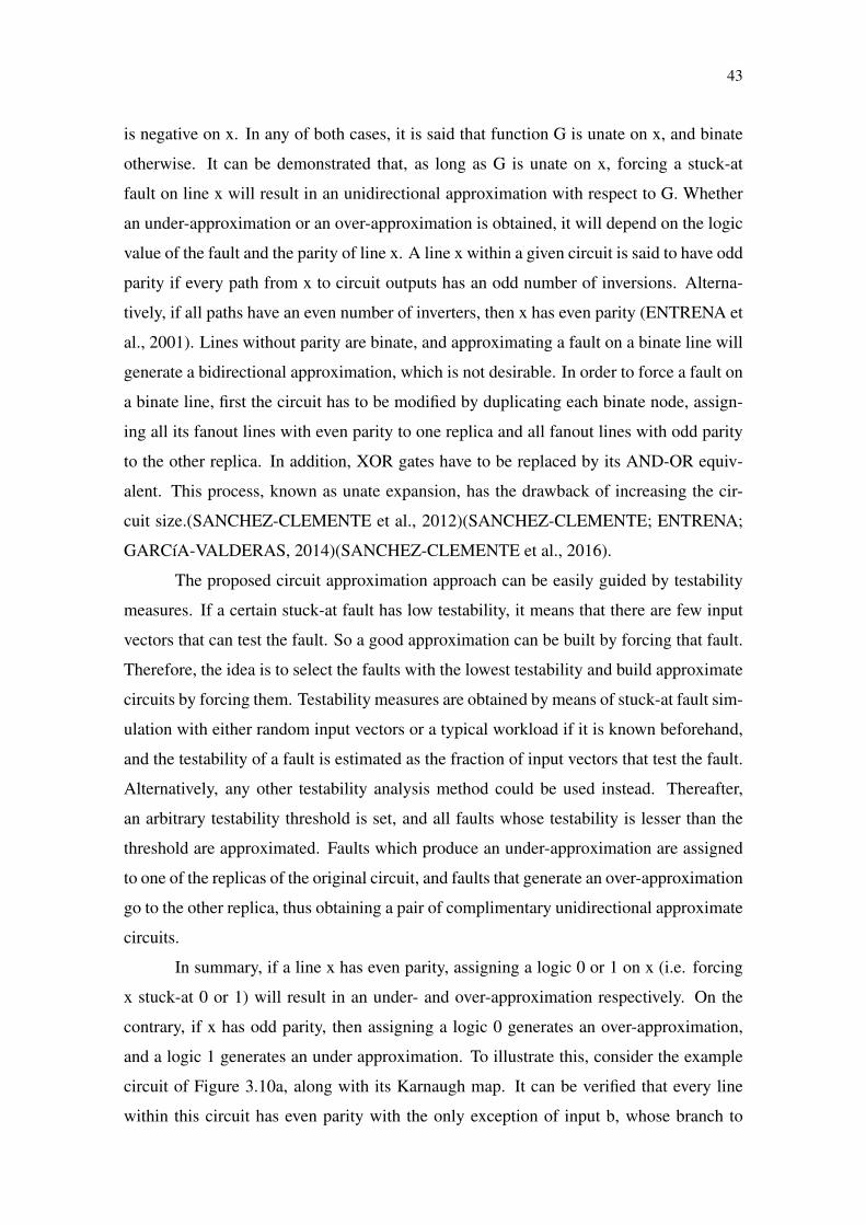
43
is negative on x. In any of both cases, it is said that function G is unate on x, and binate
otherwise. It can be demonstrated that, as long as G is unate on x, forcing a stuck-at
fault on line x will result in an unidirectional approximation with respect to G. Whether
an under-approximation or an over-approximation is obtained, it will depend on the logic
value of the fault and the parity of line x. A line x within a given circuit is said to have odd
parity if every path from x to circuit outputs has an odd number of inversions. Alterna-
tively, if all paths have an even number of inverters, then x has even parity (ENTRENA et
al., 2001). Lines without parity are binate, and approximating a fault on a binate line will
generate a bidirectional approximation, which is not desirable. In order to force a fault on
a binate line, first the circuit has to be modified by duplicating each binate node, assign-
ing all its fanout lines with even parity to one replica and all fanout lines with odd parity
to the other replica. In addition, XOR gates have to be replaced by its AND-OR equiv-
alent. This process, known as unate expansion, has the drawback of increasing the cir-
cuit size.(SANCHEZ-CLEMENTE et al., 2012)(SANCHEZ-CLEMENTE; ENTRENA;
GARCíA-VALDERAS, 2014)(SANCHEZ-CLEMENTE et al., 2016).
The proposed circuit approximation approach can be easily guided by testability
measures. If a certain stuck-at fault has low testability, it means that there are few input
vectors that can test the fault. So a good approximation can be built by forcing that fault.
Therefore, the idea is to select the faults with the lowest testability and build approximate
circuits by forcing them. Testability measures are obtained by means of stuck-at fault sim-
ulation with either random input vectors or a typical workload if it is known beforehand,
and the testability of a fault is estimated as the fraction of input vectors that test the fault.
Alternatively, any other testability analysis method could be used instead. Thereafter,
an arbitrary testability threshold is set, and all faults whose testability is lesser than the
threshold are approximated. Faults which produce an under-approximation are assigned
to one of the replicas of the original circuit, and faults that generate an over-approximation
go to the other replica, thus obtaining a pair of complimentary unidirectional approximate
circuits.
In summary, if a line x has even parity, assigning a logic 0 or 1 on x (i.e. forcing
x stuck-at 0 or 1) will result in an under- and over-approximation respectively. On the
contrary, if x has odd parity, then assigning a logic 0 generates an over-approximation,
and a logic 1 generates an under approximation. To illustrate this, consider the example
circuit of Figure 3.10a, along with its Karnaugh map. It can be verified that every line
within this circuit has even parity with the only exception of input b, whose branch to
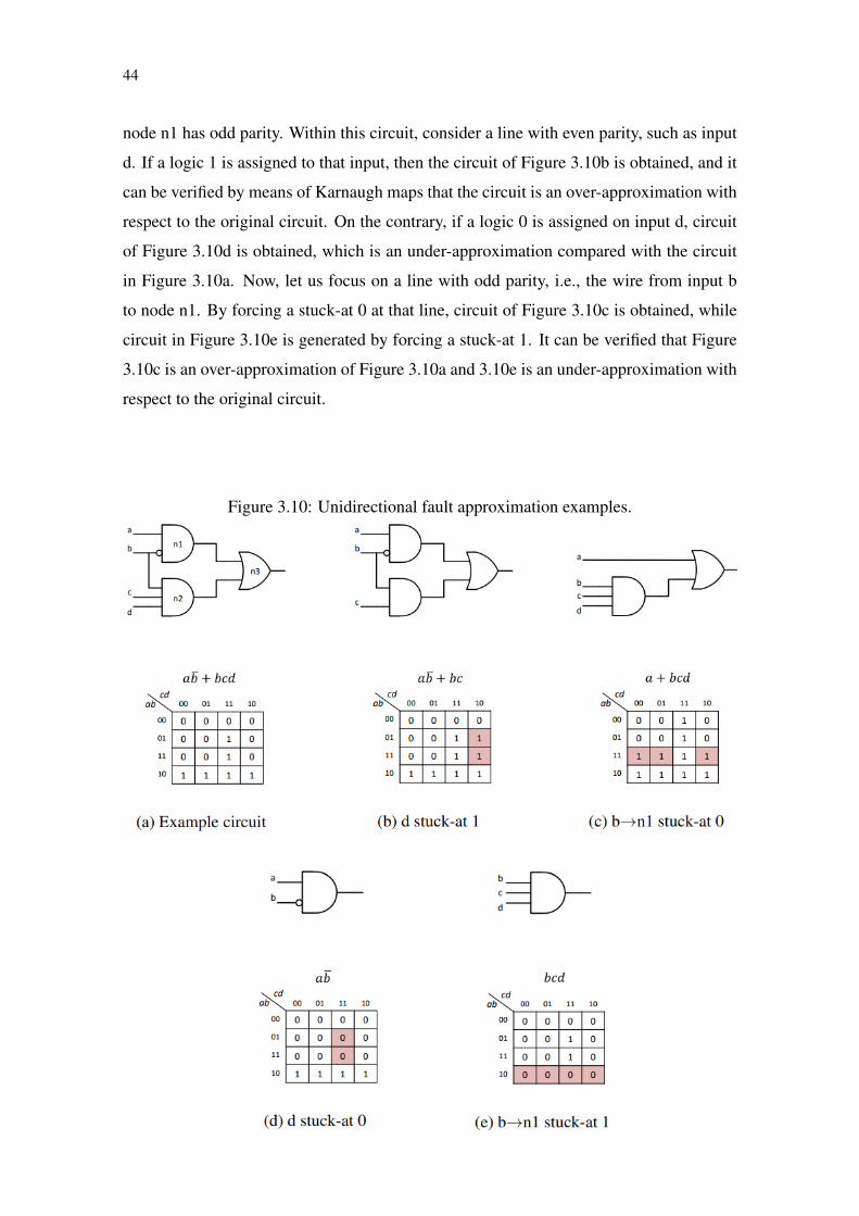
44
node n1 has odd parity. Within this circuit, consider a line with even parity, such as input
d. If a logic 1 is assigned to that input, then the circuit of Figure 3.10b is obtained, and it
can be verified by means of Karnaugh maps that the circuit is an over-approximation with
respect to the original circuit. On the contrary, if a logic 0 is assigned on input d, circuit
of Figure 3.10d is obtained, which is an under-approximation compared with the circuit
in Figure 3.10a. Now, let us focus on a line with odd parity, i.e., the wire from input b
to node n1. By forcing a stuck-at 0 at that line, circuit of Figure 3.10c is obtained, while
circuit in Figure 3.10e is generated by forcing a stuck-at 1. It can be verified that Figure
3.10c is an over-approximation of Figure 3.10a and 3.10e is an under-approximation with
respect to the original circuit.
Figure 3.10: Unidirectional fault approximation examples.

45
3.3.2 ATMR Design: Cartesian genetic programming
The evolutionary design of combinational circuits has been well established in
the past. Majority of designs in this area is conducted by Cartesian genetic program-
ming (CGP) or methods similar to CGP. Unlike GP, which uses tree representation, an
individual in CGP is represented by a directed acyclic graph of a fixed size. (SANCHEZ-
CLEMENTE et al., 2016).
The trickiest component of the evolutionary circuit design is formulating the fit-
ness function. It usually contains several objectives (functionality, area, delay etc.) where
the functionality is typically understood as the quality of the candidate circuit measured
as the number of correct output bits compared to a specified truth table (i.e. the Hamming
distance). In order to obtain a fully working circuit, all combinations of input values have
to be evaluated.
The circuit is represented as a fixed-sized cartesian grid of nr×nc nodes intercon-
nected by a feed-forward network (see Figure 3.11). Node inputs can be connected either
to one of ni primary inputs or to an output of a node in preceding L columns. Each node
has a fixed number of inputs na (usually na = 2) and can perform one of the logic func-
tions from a predefined set. Each of no primary circuit outputs can be connected either to
a primary input or to a node’s output. The area and delay of the circuit can be constrained
by changing the grid size and the L-back parameter.
Figure 3.11: Cartesian genetic programming schema. (SANCHEZ-CLEMENTE et al.,2016)
While the search is conducted at the level of genotypes (arrays of integers rep-
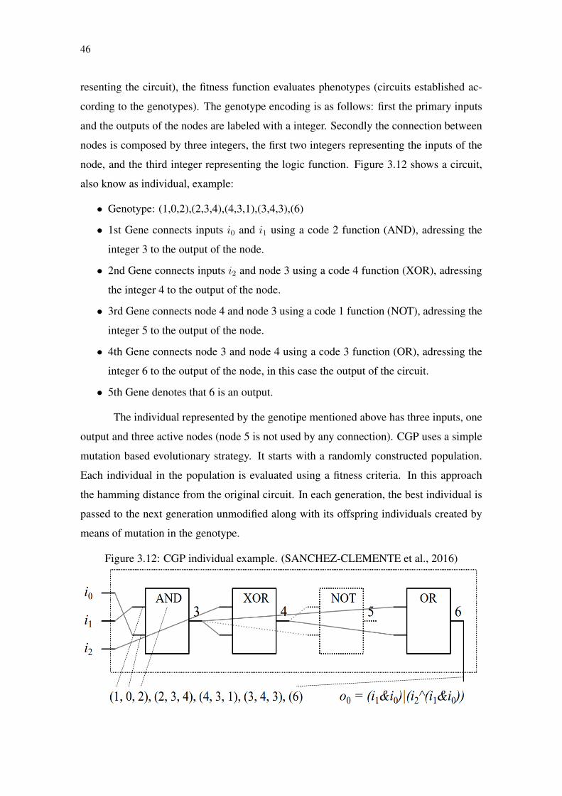
46
resenting the circuit), the fitness function evaluates phenotypes (circuits established ac-
cording to the genotypes). The genotype encoding is as follows: first the primary inputs
and the outputs of the nodes are labeled with a integer. Secondly the connection between
nodes is composed by three integers, the first two integers representing the inputs of the
node, and the third integer representing the logic function. Figure 3.12 shows a circuit,
also know as individual, example:
• Genotype: (1,0,2),(2,3,4),(4,3,1),(3,4,3),(6)
• 1st Gene connects inputs i0 and i1 using a code 2 function (AND), adressing the
integer 3 to the output of the node.
• 2nd Gene connects inputs i2 and node 3 using a code 4 function (XOR), adressing
the integer 4 to the output of the node.
• 3rd Gene connects node 4 and node 3 using a code 1 function (NOT), adressing the
integer 5 to the output of the node.
• 4th Gene connects node 3 and node 4 using a code 3 function (OR), adressing the
integer 6 to the output of the node, in this case the output of the circuit.
• 5th Gene denotes that 6 is an output.
The individual represented by the genotipe mentioned above has three inputs, one
output and three active nodes (node 5 is not used by any connection). CGP uses a simple
mutation based evolutionary strategy. It starts with a randomly constructed population.
Each individual in the population is evaluated using a fitness criteria. In this approach
the hamming distance from the original circuit. In each generation, the best individual is
passed to the next generation unmodified along with its offspring individuals created by
means of mutation in the genotype.
Figure 3.12: CGP individual example. (SANCHEZ-CLEMENTE et al., 2016)

47
4 FULL-ATMR DESIGN
In the previous chapter, we discussed what is a approximate circuit and how can
it be used in a TMR approach. It was also showed how ATMR schemes can be design
by following a main rule: F ⊆ G ⊆ H . In this chapter, we will propose a new type o
ATMR scheme, were not only two, but all three modules of the TMR are approximated,
allowing for a further overhead reduction. We called this approach Full-ATMR or simply
FATMR. Before talking about this new technique, we will talk about our first method for
the creation of approximated circuits using a boolean factoring algorithm.
4.1 Computing approximate functions with Boolean Factoring
The approach to compute the approximate functions uses a slightly modified ver-
sion of the Boolean factoring algorithm (MARTINS et al., 2010)(MARTINS; RIBAS;
REIS, 2012), called FC-ATMR tool, which uses the functional composition paradigm.
The algorithm’s input is a functional description, which can be represented by a truth ta-
ble or BDD and is assumed as the G function. This function is decomposed in cofactors
and cube-cofactors. These functions are separated using the order concept.
The order concept classifies two functions, which a function compared to other
can be smaller (has a smaller number of minterms than the original function, representing
F), larger (has a larger number of minterms than the original function, representing H) or
not comparable (Figure 4.1). A not comparable function contains some minterms of the
G function and some minterms that are not contained in G (Table 4.1). The cofactors and
cube cofactors are combined in order to generate the “allowed functions set”. This set is
used to prune functions that will not contribute to a good solution, reducing significantly
the runtime.
The next step is to store the variables in the correct polarity in a set called bucket.
These variables are stored using a bonded-pair representation, which is a tuple contain-
ing function, expression. New bonded-pairs are created from simpler bonded-pairs (i.e.,
bonded-pairs with fewer literals) computed in prior steps, in order to find the target func-
tion with less literals as possible.
The proposed algorithm besides factoring the function G, also separates all smaller
and larger functions (F and H functions, respectively) that have less literals than the G
function. The number of different bits of these functions is computed by an XOR op-
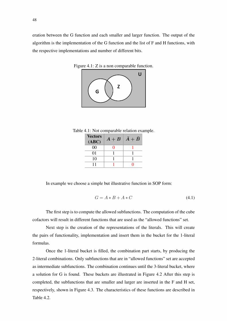
48
eration between the G function and each smaller and larger function. The output of the
algorithm is the implementation of the G function and the list of F and H functions, with
the respective implementations and number of different bits.
Figure 4.1: Z is a non comparable function.
Table 4.1: Not comparable relation example.Vectors(ABC) A + B A + B
00 0 101 1 110 1 111 1 0
In example we choose a simple but illustrative function in SOP form:
G = A ∗B + A ∗ C (4.1)
The first step is to compute the allowed subfunctions. The computation of the cube
cofactors will result in different functions that are used as the “allowed functions” set.
Next step is the creation of the representations of the literals. This will create
the pairs of functionality, implementation and insert them in the bucket for the 1-literal
formulas.
Once the 1-literal bucket is filled, the combination part starts, by producing the
2-literal combinations. Only subfunctions that are in “allowed functions” set are accepted
as intermediate subfunctions. The combination continues until the 3-literal bucket, where
a solution for G is found. These buckets are illustrated in Figure 4.2 After this step is
completed, the subfunctions that are smaller and larger are inserted in the F and H set,
respectively, shown in Figure 4.3. The characteristics of these functions are described in
Table 4.2.
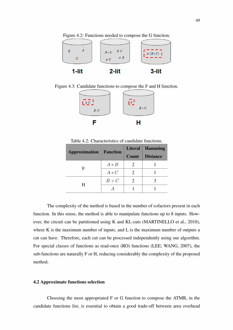
49
Figure 4.2: Functions needed to compose the G function.
Figure 4.3: Candidate functions to compose the F and H function.
Table 4.2: Characteristics of candidate functions.
Approximation FunctionLiteral
Count
Hamming
Distance
A ∗B 2 1F
A ∗ C 2 1
B + C 2 3H
A 1 1
The complexity of the method is based in the number of cofactors present in each
function. In this sense, the method is able to manipulate functions up to 8 inputs. How-
ever, the circuit can be partitioned using K and KL-cuts (MARTINELLO et al., 2010),
where K is the maximum number of inputs, and L is the maximum number of outputs a
cut can have. Therefore, each cut can be processed independently using our algorithm.
For special classes of functions as read-once (RO) functions (LEE; WANG, 2007), the
sub-functions are naturally F or H, reducing considerably the complexity of the proposed
method.
4.2 Approximate functions selection
Choosing the most appropriated F or G function to compose the ATMR, in the
candidate functions list, is essential to obtain a good trade-off between area overhead
50
and protection. When evaluating the candidate functions in a list, we must consider the
number of literals and the hamming distance (number of unprotected vectors) so that it is
possible to separate the explicitly bad functions from the functions that have some trade-
off (area/protection) between themselves.
Table 4.3 shows some candidate functions with its respective characteristics. Some
functions will be explicitly worst candidates than other ones regarding the trade off be-
tween the hamming distance and the number of literals. For example, in Table 4.3, com-
paring H6 vs H1 we can say that a trade-off do exists since H6 is bigger than H1 but has
a smaller number of unprotected vectors. However when we compare H1 vs H14 we can
verify that no trade-off exists since H1 is both smaller in size and has a smaller number
of unprotected vectors than H14, the same would be true if we compared H1 vs H3/H4,
therefore we say that from that all those function are explicitly bad functions in that list.
(ALBANDES et al., 2015b)
Table 4.3: Candidate function selection example
Cod function Literals Hamming
H6 ((!D + !C) * (!E + !F)) 4 3
H1 (!D + !C) 2 15
H14 ((!E + !F) * (!B + (!D + !A))) 5 9
H3 (!B + (!D + !A)) 3 23
H4 ((!B + !D) + !C) 3 23
4.3 Full-ATMR Scheme
For the ATMR to work correctly with three different modules the main rule dic-
tates that F ⊆ G ⊆ H , therefore obtaining a composition of circuits that guarantees that
only one module may diverge from the other two at any given input vector in the absence
of faults. In the Full-ATMR we will not restrict the design with the usual G, F and H
composition, instead we propose a scheme that also substitute circuit G for a approximate
circuit (F or H).
The most important rule of the Full-ATMR scheme is that only one module may
differ from the other two modules to be able to compute the correct value through the
majority voter when using spatial redundancy, therefore the voter will have two correct
outputs against the one divergent output. This can be achieved even when all the modules
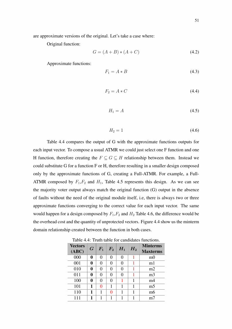
51
are approximate versions of the original. Let’s take a case where:
Original function:
G = (A + B) ∗ (A + C) (4.2)
Approximate functions:
F1 = A ∗B (4.3)
F2 = A ∗ C (4.4)
H1 = A (4.5)
H2 = 1 (4.6)
Table 4.4 compares the output of G with the approximate functions outputs for
each input vector. To compose a usual ATMR we could just select one F function and one
H function, therefore creating the F ⊆ G ⊆ H relationship between them. Instead we
could substitute G for a function F or H, therefore resulting in a smaller design composed
only by the approximate functions of G, creating a Full-ATMR. For example, a Full-
ATMR composed by F1,F2 and H1, Table 4.5 represents this design. As we can see
the majority voter output always match the original function (G) output in the absence
of faults without the need of the original module itself, i.e, there is always two or three
approximate functions converging to the correct value for each input vector. The same
would happen for a design composed by F1,F2 and H2 Table 4.6, the difference would be
the overhead cost and the quantity of unprotected vectors. Figure 4.4 show us the minterm
domain relationship created between the function in both cases.
Table 4.4: Truth table for candidates functions.Vectors(ABC) G F1 F2 H1 H2
MintermsMaxterms
000 0 0 0 0 1 m0001 0 0 0 0 1 m1010 0 0 0 0 1 m2011 0 0 0 0 1 m3100 0 0 0 1 1 m4101 1 0 1 1 1 m5110 1 1 0 1 1 m6111 1 1 1 1 1 m7

52
Table 4.5: Truth table for a FATMR composed by F1,F2 and H1.Vectors(ABC) F1 F2 H1
Voteroutput
000 0 0 0 0001 0 0 0 0010 0 0 0 0011 0 0 0 0100 0 0 1 0101 0 1 1 1110 1 0 1 1111 1 1 1 1
Figure 4.4: Graphical representation of the relationship of functions for a Full-ATMRcomposed by F1,F2 and Hx. Grey area is protected, i.e, all functions converge to thesame value.
Not all approximate functions can compose a Full-ATMR scheme. For two (or
even three) functions of the same type (F or H) compose the design it is necessary that
none of them diverge from G at same input vector. For instance, F1 and F2 are both under-
approximate but they diverge from G in a different set of minterms (m5 for F1 and m6 for
F2). We can’t design a Full-ATMR composed by H1 and H2 and any other function. In
this case (Table 4.7) both H1 and H2 and diverge from G on the same input vector (100),
therefore resulting in the incorrect value of the majority voter output in the absence of
faults.
Assuming that for a given design we could find two H functions to compose the
Full-ATMR, Figure 4.5 represents the relationship for a Full-ATMR composed by two
H functions and one F function. Another possibility is that all the functions were of
the same kind (F or H), in this case Figure 4.6 represents the relationship for a Full-
ATMR composed by three functions of the same type, F (under-approximate) and H (over-
approximate).

53
Table 4.6: Truth table for a FATMR composed by F1,F2 and H2.Vectors(ABC) F1 F2 H1
Voteroutput
000 0 0 1 0001 0 0 1 0010 0 0 1 0011 0 0 1 0100 0 0 1 0101 0 1 1 1110 1 0 1 1111 1 1 1 1
Table 4.7: Truth table for a FATMR composed by F1,H1 and H2.Vectors(ABC) F1 H1 H2
Voteroutput
000 0 0 1 0001 0 0 1 0010 0 0 1 0011 0 0 1 0100 0 1 1 0⇒1101 0 1 1 1110 1 1 1 1111 1 1 1 1
4.4 Full-ATMR results
The methodology used in for these results is composed of four main steps. First,
we compute the list of possible approximate functions F and H to use in the ATMR
or FATMR designs sing the factoring algorithm described in section 4.1. Second, we
choose the functions to compose the TMR scheme as told in section 4.2. Third, we map
the function though an academic state-of-the-art logic synthesis tool ABC (BRAYTON;
MISHCHENKO, 2010), in conjunction with a library, containing the following cells: INV,
NAND2-3-4, NOR2-3-4, OAI21, OAI22, AOI21 and AOI22. We used this library to gen-
erate a gate netlist in Verilog, where we translate the gate level description generated by
ABC to a transistor level circuit using a tool developed by. Finally we inject single faults
in transistor level of the circuits using Modelsim to test the circuits susceptibility to SET.
Figure 4.7 shows the flow of the methodology.
In order to evaluate the effective fault masking capability of each ATMR and
FATMR scheme built, a fault injection tool is used. The tool was developed using Python
and integrated with ModelSim, using Verilog. A SET can be emulated in logical level,
through ModelSim, by forcing a change in the state of a node. This simulates an energetic
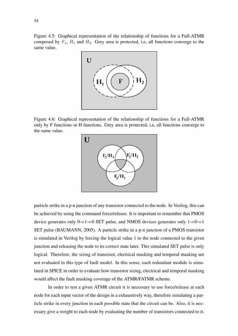
54
Figure 4.5: Graphical representation of the relationship of functions for a Full-ATMRcomposed by Fx, H1 and H2. Grey area is protected, i.e, all functions converge to thesame value.
Figure 4.6: Graphical representation of the relationship of functions for a Full-ATMRonly by F functions or H functions. Grey area is protected, i.e, all functions converge tothe same value.
particle strike in a p-n junction of any transistor connected to the node. In Verilog, this can
be achieved by using the command force/release. It is important to remember that PMOS
device generates only 0⇒1⇒0 SET pulse, and NMOS devices generates only 1⇒0⇒1
SET pulse (BAUMANN, 2005). A particle strike in a p-n junction of a PMOS transistor
is simulated in Verilog by forcing the logical value 1 to the node connected to the given
junction and releasing the node to its correct state later. This simulated SET pulse is only
logical. Therefore, the sizing of transistor, electrical masking and temporal masking are
not evaluated in this type of fault model. In this sense, each redundant module is simu-
lated in SPICE in order to evaluate how transistor sizing, electrical and temporal masking
would affect the fault masking coverage of the ATMR/FATMR scheme.
In order to test a given ATMR circuit it is necessary to use force/release at each
node for each input vector of the design in a exhaustively way, therefore simulating a par-
ticle strike in every junction in each possible state that the circuit can be. Also, it is nec-
essary give a weight to each node by evaluating the number of transistors connected to it.

55
This step is responsible to generate a transistor level description of the ATMR/FTMR and
determine the amount of unprotected p-n junctions of the ATMR and FATMR schemes.
We do not inject SET in the majority voters.
Figure 4.7: Methodology used to generate results for ATMR/FATMR circuits.
4.4.1 Case-study 1
First case of study was created based on the 5 input function represented by G:
G = (a + b) ∗ ((c ∗ b) + ((a + e) ∗ ((a ∗ (c + e)) + d))) (4.7)
Table 4.8 and Table 4.9 shows a list of selected approximate functions F and H for
the case-study circuit 1. Table 4.10 shows the characteristics of each ATMR and FATMR
schemes composed with different selected approximate functions in terms of unprotected
vectors, fault masking coverage and area overhead. The schemes in the table are ordered
increasingly using the area overhead as order criteria. Notice that each scheme has a
different number of unprotected vectors and unprotected junctions. The highest fault
masking coverage is given by the schemes that present the lowest number of unprotected
vectors and junctions. The area is measured by the number of transistors. One can observe
that it is possible to maintain the maximum protected p-n junction ratio of 98.88% (60 p-n

56
junctions of 5248) with only 165% area overhead when using ATMR; and a maximum of
94.66% protected p-n junction ratio (205 p-n junctions of 3840) with only an 88% area
when using FATMR.
Table 4.8: Under-approximations for G
Under-approximated functionsHamming
Distance
F1 a ∗ b ∗ c 10
F2 a ∗ b ∗ (d + e) 8
F3 a ∗ b ∗ d + a ∗ e 6
F4 (a + b) ∗ (c ∗ b + d ∗ e) 5
F5 (a + b) ∗ (((a + e) ∗ ((a ∗ (c + e)) + d))) 3
Table 4.9: Over-approximations for G
Over-approximated functionsHamming
Distance
H1 a + b 10
H2 b + (a ∗ (c + e)) 8
H3 a ∗ b + (a ∗ (c + e)) 6
H4 a ∗ b + (a ∗ (c + e ∗ d)) 4
H5 d ∗ e + a ∗ b + c ∗ a ∗ b 3
H6 a ∗ d ∗ e + a ∗ b + c ∗ a ∗ b 1
4.4.2 Case-study 2
The second case of study is an ATMR design of a 4-bit adder. The 4-bit adder
is composed by one half-adder at bit 0 and other 3 full-adders. Table 4.11 shows the
approximate logic functions used for the Sum and Carry outputs for both cases. Figure
4.8 shows the scheme of the 4-bit ripple-carry adder with TMR or ATMR technique.
The original full-adder (G) used has a size of 28 transistors (complex gate). The
under-approximate full-adder (F) has a size of 12 transistors (two AND2 gates). The
over-approximate full-adder (H) has a size of 12 transistors (two OR2 gates). The original
half-adder (G) has a size of 16 transistors (one XOR2, one AND2 and one inverter). The
under-approximate full-adder (F) has a size of 6 transistors (one NOR2 gate and one
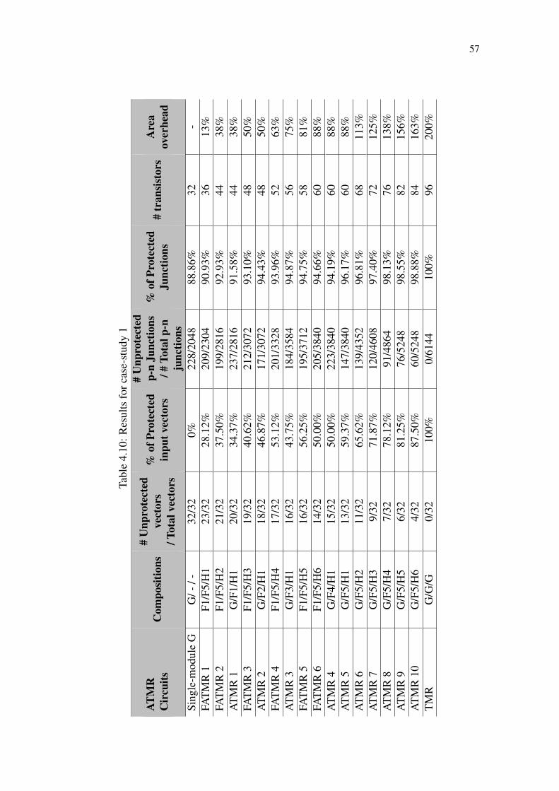
57
Tabl
e4.
10:R
esul
tsfo
rcas
e-st
udy
1
ATM
RC
ircu
itsC
ompo
sitio
ns#
Unp
rote
cted
vect
ors
/Tot
alve
ctor
s
%of
Prot
ecte
din
putv
ecto
rs
#U
npro
tect
edp-
nJu
nctio
ns/#
Tota
lp-n
junc
tions
%of
Prot
ecte
dJu
nctio
ns#
tran
sist
ors
Are
aov
erhe
ad
Sing
le-m
odul
eG
G/-
/-32
/32
0%22
8/20
4888
.86%
32-
FAT
MR
1F1
/F5/
H1
23/3
228
.12%
209/
2304
90.9
3%36
13%
FAT
MR
2F1
/F5/
H2
21/3
237
.50%
199/
2816
92.9
3%44
38%
AT
MR
1G
/F1/
H1
20/3
234
.37%
237/
2816
91.5
8%44
38%
FAT
MR
3F1
/F5/
H3
19/3
240
.62%
212/
3072
93.1
0%48
50%
AT
MR
2G
/F2/
H1
18/3
246
.87%
171/
3072
94.4
3%48
50%
FAT
MR
4F1
/F5/
H4
17/3
253
.12%
201/
3328
93.9
6%52
63%
AT
MR
3G
/F3/
H1
16/3
243
.75%
184/
3584
94.8
7%56
75%
FAT
MR
5F1
/F5/
H5
16/3
256
.25%
195/
3712
94.7
5%58
81%
FAT
MR
6F1
/F5/
H6
14/3
250
.00%
205/
3840
94.6
6%60
88%
AT
MR
4G
/F4/
H1
15/3
250
.00%
223/
3840
94.1
9%60
88%
AT
MR
5G
/F5/
H1
13/3
259
.37%
147/
3840
96.1
7%60
88%
AT
MR
6G
/F5/
H2
11/3
265
.62%
139/
4352
96.8
1%68
113%
AT
MR
7G
/F5/
H3
9/32
71.8
7%12
0/46
0897
.40%
7212
5%A
TM
R8
G/F
5/H
47/
3278
.12%
91/4
864
98.1
3%76
138%
AT
MR
9G
/F5/
H5
6/32
81.2
5%76
/524
898
.55%
8215
6%A
TM
R10
G/F
5/H
64/
3287
.50%
60/5
248
98.8
8%84
163%
TM
RG
/G/G
0/32
100%
0/61
4410
0%96
200%
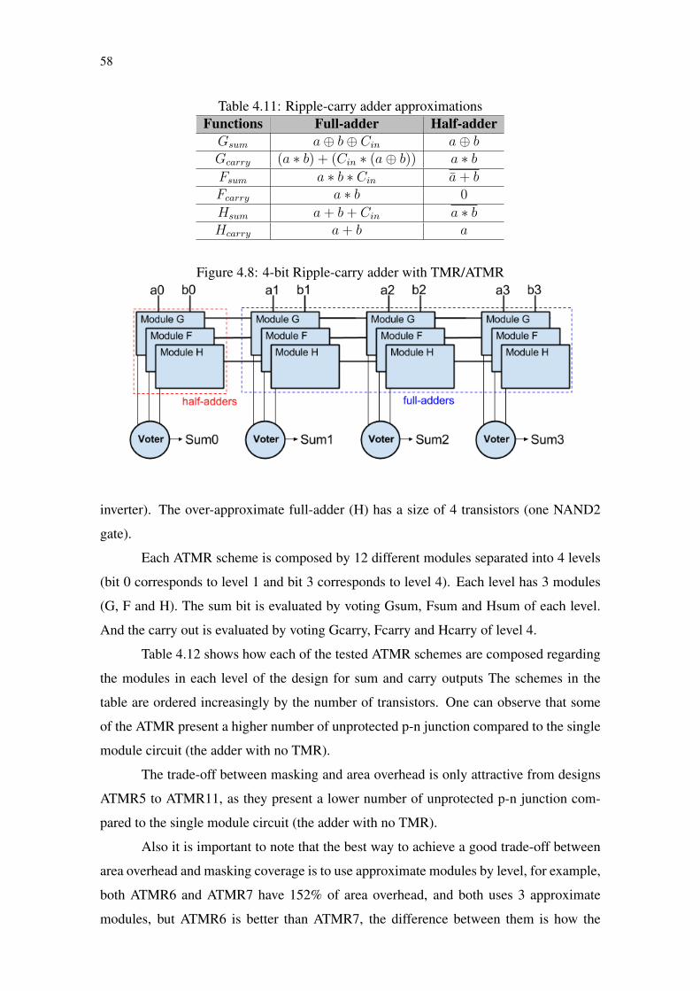
58
Table 4.11: Ripple-carry adder approximationsFunctions Full-adder Half-adder
Gsum a⊕ b⊕ Cin a⊕ bGcarry (a ∗ b) + (Cin ∗ (a⊕ b)) a ∗ bFsum a ∗ b ∗ Cin a + bFcarry a ∗ b 0
Hsum a + b + Cin a ∗ bHcarry a + b a
Figure 4.8: 4-bit Ripple-carry adder with TMR/ATMR
inverter). The over-approximate full-adder (H) has a size of 4 transistors (one NAND2
gate).
Each ATMR scheme is composed by 12 different modules separated into 4 levels
(bit 0 corresponds to level 1 and bit 3 corresponds to level 4). Each level has 3 modules
(G, F and H). The sum bit is evaluated by voting Gsum, Fsum and Hsum of each level.
And the carry out is evaluated by voting Gcarry, Fcarry and Hcarry of level 4.
Table 4.12 shows how each of the tested ATMR schemes are composed regarding
the modules in each level of the design for sum and carry outputs The schemes in the
table are ordered increasingly by the number of transistors. One can observe that some
of the ATMR present a higher number of unprotected p-n junction compared to the single
module circuit (the adder with no TMR).
The trade-off between masking and area overhead is only attractive from designs
ATMR5 to ATMR11, as they present a lower number of unprotected p-n junction com-
pared to the single module circuit (the adder with no TMR).
Also it is important to note that the best way to achieve a good trade-off between
area overhead and masking coverage is to use approximate modules by level, for example,
both ATMR6 and ATMR7 have 152% of area overhead, and both uses 3 approximate
modules, but ATMR6 is better than ATMR7, the difference between them is how the
59
approximate modules are spread. ATMR6 uses two approximate module in level 4 and
one in level 3 of the circuit, ATMR7 allocates one module for each level, starting from
level 2 to level 4. Something similar can be seen when we compare ATMR6 to ATMR5,
were ATMR5 has 4 approximate module, two for level 3 and two for level 4, showing a
trade-off when compared to ATMR6.
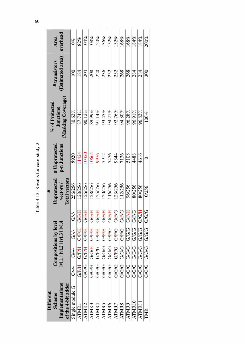
60
Tabl
e4.
12:R
esul
tsfo
rcas
e-st
udy
2
Diff
eren
tSc
hem
eIm
plem
enta
tions
ofth
e4-
bita
dder
Com
posi
tions
byle
vel
lvl.1
|lvl
.2|l
vl.3
|lvl
.4
#U
npro
tect
edve
ctor
s/To
talv
ecto
rs
#U
npro
tect
edp-
nJu
nctio
ns
%of
Prot
ecte
dJu
nctio
ns(M
aski
ngC
over
age)
#tr
ansi
stor
s(E
stim
ated
area
)A
rea
over
head
Sing
lem
odul
eG
G/-
/-G
/-/-
G/-
/-G
/-/-
256/
256
9920
80.6
3%10
00%
AT
MR
1G
/F/H
G/F
/HG
/F/H
G/F
/H12
8/25
611
424
87.7
4%18
482
%A
TM
R2
G/G
/GG
/F/H
G/F
/HG
/F/H
126/
256
1032
090
.12%
204
104%
AT
MR
3G
/G/H
G/G
/HG
/F/H
G/F
/H12
8/25
610
664
89.9
9%20
810
8%A
TM
R4
G/G
/GG
/F/G
G/F
/HG
/F/H
125/
256
9976
91.1
4%22
012
0%A
TM
R5
G/G
/GG
/G/G
G/F
/HG
/F/H
120/
256
7912
93.4
5%23
613
6%A
TM
R6
G/G
/GG
/G/G
G/F
/GG
/F/H
116/
256
7476
94.2
1%25
215
2%A
TM
R7
G/G
/GG
/F/G
G/F
/GG
/F/G
123/
256
9344
92.7
6%25
215
2%A
TM
R8
G/G
/GG
/G/G
G/F
/GG
/F/G
112/
256
7136
94.8
0%26
816
8%A
TM
R9
G/G
/GG
/G/G
G/G
/GG
/F/H
96/2
5651
0896
.28%
268
168%
AT
MR
10G
/G/G
G/G
/GG
/G/G
G/F
/G80
/256
4488
96.9
1%28
418
4%A
TM
R11
G/G
/GG
/G/G
G/G
/GG
/G/H
80/2
5646
1696
.83%
284
184%
TM
RG
/G/G
G/G
/GG
/G/G
G/G
/G0/
256
010
0%30
020
0%
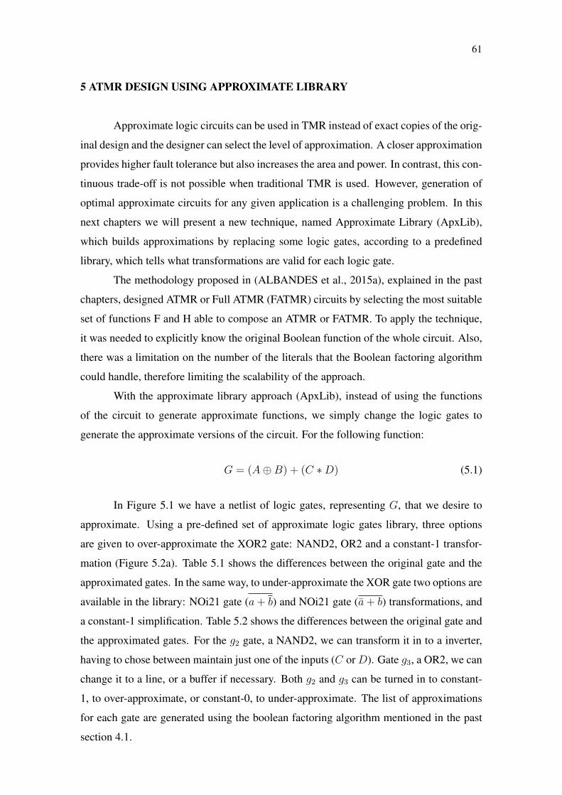
61
5 ATMR DESIGN USING APPROXIMATE LIBRARY
Approximate logic circuits can be used in TMR instead of exact copies of the orig-
inal design and the designer can select the level of approximation. A closer approximation
provides higher fault tolerance but also increases the area and power. In contrast, this con-
tinuous trade-off is not possible when traditional TMR is used. However, generation of
optimal approximate circuits for any given application is a challenging problem. In this
next chapters we will present a new technique, named Approximate Library (ApxLib),
which builds approximations by replacing some logic gates, according to a predefined
library, which tells what transformations are valid for each logic gate.
The methodology proposed in (ALBANDES et al., 2015a), explained in the past
chapters, designed ATMR or Full ATMR (FATMR) circuits by selecting the most suitable
set of functions F and H able to compose an ATMR or FATMR. To apply the technique,
it was needed to explicitly know the original Boolean function of the whole circuit. Also,
there was a limitation on the number of the literals that the Boolean factoring algorithm
could handle, therefore limiting the scalability of the approach.
With the approximate library approach (ApxLib), instead of using the functions
of the circuit to generate approximate functions, we simply change the logic gates to
generate the approximate versions of the circuit. For the following function:
G = (A⊕B) + (C ∗D) (5.1)
In Figure 5.1 we have a netlist of logic gates, representing G, that we desire to
approximate. Using a pre-defined set of approximate logic gates library, three options
are given to over-approximate the XOR2 gate: NAND2, OR2 and a constant-1 transfor-
mation (Figure 5.2a). Table 5.1 shows the differences between the original gate and the
approximated gates. In the same way, to under-approximate the XOR gate two options are
available in the library: NOi21 gate (a + b) and NOi21 gate (a + b) transformations, and
a constant-1 simplification. Table 5.2 shows the differences between the original gate and
the approximated gates. For the g2 gate, a NAND2, we can transform it in to a inverter,
having to chose between maintain just one of the inputs (C or D). Gate g3, a OR2, we can
change it to a line, or a buffer if necessary. Both g2 and g3 can be turned in to constant-
1, to over-approximate, or constant-0, to under-approximate. The list of approximations
for each gate are generated using the boolean factoring algorithm mentioned in the past
section 4.1.
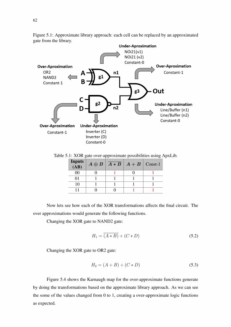
62
Figure 5.1: Approximate library approach: each cell can be replaced by an approximatedgate from the library.
Table 5.1: XOR gate over-approximate possibilities using ApxLib.Inputs(AB) A⊕B A ∗B A + B Const-1
00 0 1 0 101 1 1 1 110 1 1 1 111 0 0 1 1
Now lets see how each of the XOR transformations affects the final circuit. The
over approximations would generate the following functions.
Changing the XOR gate to NAND2 gate:
H1 = (A ∗B) + (C ∗D) (5.2)
Changing the XOR gate to OR2 gate:
H2 = (A + B) + (C ∗D) (5.3)
Figure 5.4 shows the Karnaugh map for the over-approximate functions generate
by doing the transformations based on the approximate library approach. As we can see
the some of the values changed from 0 to 1, creating a over-approximate logic functions
as expected.

63
Figure 5.2: Approximate library approach: approximations possibilities for g1 XOR2gate.
(a) Over-approximations for the g1 XOR2gate
(b) Under-approximations for the g1 XOR2gate
Figure 5.3: Approximate library approach: approximations possibilities for g2 and g3gates.
(a) Under-approximations for the g2NAND2 gate
(b) Under-approximations for the g3 OR2gate
The under approximations would generate the following functions.
Changing the XOR gate to NOi21 type 1 gate:
F1 = (A + B) + (C ∗D) (5.4)
Changing the XOR gate to NOi21 type 2 gate:
F2 = (A + B) + (C ∗D) (5.5)
Figure 5.5 shows the Karnaugh map for the under-approximate functions generate
by doing the transformations based on the approximate library approach. As we can see
the some of the values changed from 1 to 0, creating a under-approximate logic functions
as expected.

64
Table 5.2: XOR gate under-approximate possibilities using ApxLib.Inputs(AB) A⊕B A + B A + B Const-0
00 0 0 0 001 1 0 1 010 1 1 0 011 0 0 0 0
Figure 5.4: Karnaugh map for the final over-approximate functions of G.
(a) G = (A⊕B) + (C ∗D)
(b) H1 = (A ∗B) + (C ∗D) (c) H2 = (A+B) + (C ∗D)
Figure 5.5: Karnaugh map for the final under-approximate functions of G.
(a) G = (A⊕B) + (C ∗D)
(b) F1 = (A+B) + (C ∗D)) (c) F2 = (A+B) + (C ∗D))
65
5.1 Parity analysis
Another major point in the approach is the evaluation of the parity of the gates. If
the parity is not calculated correctly the circuit generated may not be functionally compat-
ible in the final ATMR scheme. A logic function Fn(x1, x2, ..., xn) is said to be positive
in xi if, expressing Fn as a sum of products (SOP), xi does not appear complemented.
Analogously, Fn is negative in xi if xi only appears complemented in the sum of prod-
ucts. This holds true not only for the function inputs, but also for any intermediate result
by performing a variable change. A logic function F is said to be unate in xi if F is either
positive or negative in xi, otherwise it is binate in xi. When considering multiple output
functions it is said that F is unate in xi if either every partial logic function Fj correspond-
ing to output Oj is positive in xi, or negative instead. Otherwise it is binate in xi. It must
be noted that if some outputs are positive in xi while the rest are negative, then the whole
function is binate in xi.(SANCHEZ-CLEMENTE; ENTRENA; GARCíA-VALDERAS,
2014)
A logic circuit is the logical representation of a multiple output logic function. It
is said that a node, line or gate xi within a logic circuit has even parity if every logical
path from xi to the outputs of the circuit has an even number of inversions. Analogously,
xi has odd parity if all propagation paths form xi to the outputs have an odd number of
inversions. If node, line or gate xi within logic circuit C has even or odd parity, then C is
positive or negative in xi respectively, which implies that C is unate in xi . Otherwise, xi
has no parity, and therefore C is binate in xi (SANCHEZ-CLEMENTE et al., 2012).
Parities in a circuit can be computed by traversing the network from primary out-
puts of the circuit to primary inputs of the circuit. In network terms, a node nx is positive
(negative) in x if all paths from x to the primary outputs have an even (odd) number of
inversions. In such a case, we say that node nx has an even (odd) parity. If a node nx is
binate in x, then there are at least two paths from nx to the primary outputs with different
parities, and we say that node nx has no parity (also saying that it has a binate property).
The gate, or input, parity in a circuit is defined by the node which its output is connected.
Figure 5.6 will serve as an example for the parity evaluation of the gates in the
circuit. The start point for the traversal of the circuit is the output O1. We will evaluate
first the nodes and gates parity relation to the circuit output O1. O1 itself is classified as
having a positive (even) parity. From O1 we go to gate g1, classifying it as a positive parity
gate since its output is connected only to the positive node (even parity) O1. Traversing
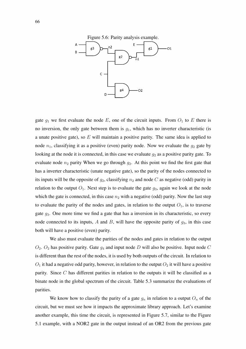
66
Figure 5.6: Parity analysis example.
gate g1 we first evaluate the node E, one of the circuit inputs. From O1 to E there is
no inversion, the only gate between them is g1, which has no inverter characteristic (is
a unate positive gate), so E will maintain a positive parity. The same idea is applied to
node n1, classifying it as a positive (even) parity node. Now we evaluate the g2 gate by
looking at the node it is connected, in this case we evaluate g2 as a positive parity gate. To
evaluate node n2 parity When we go through g2. At this point we find the first gate that
has a inverter characteristic (unate negative gate), so the parity of the nodes connected to
its inputs will be the opposite of g2, classifying n2 and node C as negative (odd) parity in
relation to the output O1. Next step is to evaluate the gate g3, again we look at the node
which the gate is connected, in this case n2 with a negative (odd) parity. Now the last step
to evaluate the parity of the nodes and gates, in relation to the output O1, is to traverse
gate g3. One more time we find a gate that has a inversion in its characteristic, so every
node connected to its inputs, A and B, will have the opposite parity of g3, in this case
both will have a positive (even) parity.
We also must evaluate the parities of the nodes and gates in relation to the output
O2. O2 has positive parity. Gate g4 and input node D will also be positive. Input node C
is different than the rest of the nodes, it is used by both outputs of the circuit. In relation to
O1 it had a negative odd parity, however, in relation to the output O2 it will have a positive
parity. Since C has different parities in relation to the outputs it will be classified as a
binate node in the global spectrum of the circuit. Table 5.3 summarize the evaluations of
parities.
We know how to classify the parity of a gate gn in relation to a output On of the
circuit, but we must see how it impacts the approximate library approach. Let’s examine
another example, this time the circuit, is represented in Figure 5.7, similar to the Figure
5.1 example, with a NOR2 gate in the output instead of an OR2 from the previous gate

67
Table 5.3: Parity analysis summary.NodeGate O1 O2 Global
g1 positive - positiveg2 positive - positiveg3 negative - negativeg4 positive - positiven1 positive - positiven2 negative - negativeA positive - positiveB positive - positiveC negative positive no-parityD - positive positiveE positive - positive
transformation example. The original function is:
G2 = (A⊕B) + (C ∗D) (5.6)
Figure 5.7: Approximate library approach, where each cell can be replaced by an approx-imate function from the library.
Now we will approximate the XOR2 gate to a OR2 gate, with the intention of
creating a over-approximated function, and the resulting function is:
Q1 = (A + B) + (C ∗D) (5.7)
If we evaluate the Karnaugh map comparing G2 and Q1, in Figure 5.8, we will see
that the function created is a under-approximate instead of the desired over-approximated
function. This happens because of the XOR2 gate parity. The XOR2 gate has a negative
parity, this causes the approximations in the library to be swapped, and, as we have seen,

68
by selecting a over-approximation of a negative gate we end up with a under-approximated
logic.
If we wanted to create a over-approximate circuit, by only changing the negative
parity XOR2 gate, we should take one of the approximations from the under-approximate
list. Figure 5.8 represents the creation of a over-approximate function using a under-
approximate transformation of a negative parity gate, the XOR2. The resulting function
is:
Q2 = (A + B) + (C ∗D) (5.8)
Figure 5.8: Karnaugh map for the final under-approximate functions of G.
(a) G2 = (A⊕B) + (C ∗D) (b) Q1 = (A+B) + (C ∗D)
Figure 5.9: Karnaugh map for the final under-approximate functions of G.
(a) G2 = (A⊕B) + (C ∗D) (b) Q2 = (A+B) + (C ∗D)
5.2 Binate gate
Another important point are the gates that have a binate property itself. XOR
and XNOR gates are examples of binate gates, so when we traverse one of those gates it
implies a no-parity (binate) characteristic in the next nodes/gates, and those nodes/gates
do the same for the next ones. But what exactly is the problem with a no-parity gate? Lets
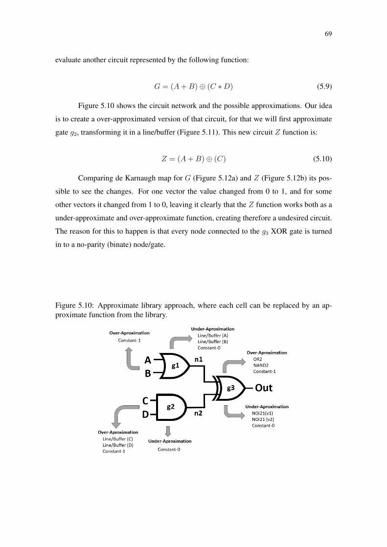
69
evaluate another circuit represented by the following function:
G = (A + B)⊕ (C ∗D) (5.9)
Figure 5.10 shows the circuit network and the possible approximations. Our idea
is to create a over-approximated version of that circuit, for that we will first approximate
gate g2, transforming it in a line/buffer (Figure 5.11). This new circuit Z function is:
Z = (A + B)⊕ (C) (5.10)
Comparing de Karnaugh map for G (Figure 5.12a) and Z (Figure 5.12b) its pos-
sible to see the changes. For one vector the value changed from 0 to 1, and for some
other vectors it changed from 1 to 0, leaving it clearly that the Z function works both as a
under-approximate and over-approximate function, creating therefore a undesired circuit.
The reason for this to happen is that every node connected to the g3 XOR gate is turned
in to a no-parity (binate) node/gate.
Figure 5.10: Approximate library approach, where each cell can be replaced by an ap-proximate function from the library.

70
Figure 5.11: Approximate library approach, where each cell can be replaced by an ap-proximate function from the library.
Figure 5.12: Karnaugh map for the final under-approximate functions of G.
(a) G3 = (A+B)⊕ (C ∗D) (b) Z = (A+B)⊕ (C)
In this case there is a simple way to resolve the binate problem: transform the g3
gate in to a non-binate over-approximated gate. Looking to the option for the XOR2 gate
we can change it to a OR2 gate. The new circuit, in Figure 5.13, is represented by the
function:
H1 = (A + B) + (C ∗D) (5.11)
Figure 5.13: Approximate library approach, where each cell can be replaced by an ap-proximate function from the library.
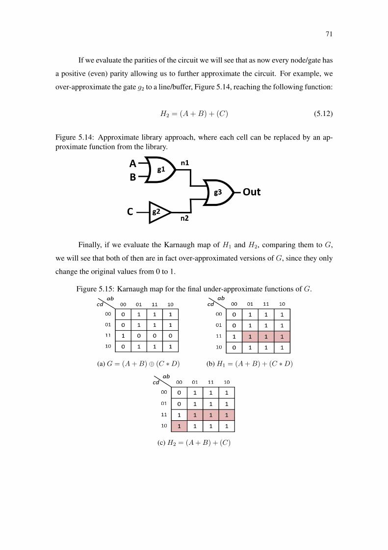
71
If we evaluate the parities of the circuit we will see that as now every node/gate has
a positive (even) parity allowing us to further approximate the circuit. For example, we
over-approximate the gate g2 to a line/buffer, Figure 5.14, reaching the following function:
H2 = (A + B) + (C) (5.12)
Figure 5.14: Approximate library approach, where each cell can be replaced by an ap-proximate function from the library.
Finally, if we evaluate the Karnaugh map of H1 and H2, comparing them to G,
we will see that both of then are in fact over-approximated versions of G, since they only
change the original values from 0 to 1.
Figure 5.15: Karnaugh map for the final under-approximate functions of G.
(a) G = (A+B)⊕ (C ∗D) (b) H1 = (A+B) + (C ∗D)
(c) H2 = (A+B) + (C)
72
6 APPROXIMATE LIBRARY APPROACH USING GENETIC ALGORITHM
Many real-world optimization problems are extremely difficult and complex in
terms of number of variables, nature of the objective function, many local optimal, con-
tinuous or discrete search space, required computation time and resources, etc. in various
domains including service, commerce and engineering (AMOUZGAR, 2012). The Ap-
proximate Library approach share the same complexity as some of those problems, each
modification in the circuit generates a large new number of possible modifications, in-
creasing the list of solutions very fast. Figure 6.1 shows three successive approximations
for the same original circuit, each transformation we choose opens a new set of possible
solutions.
Genetic algorithm is an inspiration of the selection process of nature, where in a
competition the stronger individuals will survive. In nature each member of a population
competes for food, water and territory, also strive for attracting a mate is another aspect
of nature. It is obvious the stronger individuals have a better chance for reproduction and
creating offspring, while the poor performers have less offspring or even none. Conse-
quently the genes of the strong or fit individuals will increase in the population. Offspring
created by two fit individual (parents) has a potential to have a better fitness compared to
both parents called super-fit offspring. By this principle the initial population evolves to
a better suited population to their environment in each generation (AMOUZGAR, 2012).
The idea of using a Multi-Objective Optmization Genetic Algorithm (MOOGA),
(AMOUZGAR, 2012)(SERRANO-CASES et al., 2016), with the ApxLib approach, (AL-
BANDES et al., 2018b), aim to do a blind search within all possible solution space, which
have all possible ATMR configuration, and then with the Multi-Objective Optimization
sorting we selected the best configurations that reduced the area and maximize the fault
coverage. We named this approach as MOOGA+ApxLib.

73
Figure 6.1: Exponential growth of solution for the ApxLib approach.
(a) 1st interaction
(b) 2nd interaction
(c) 3rd interaction
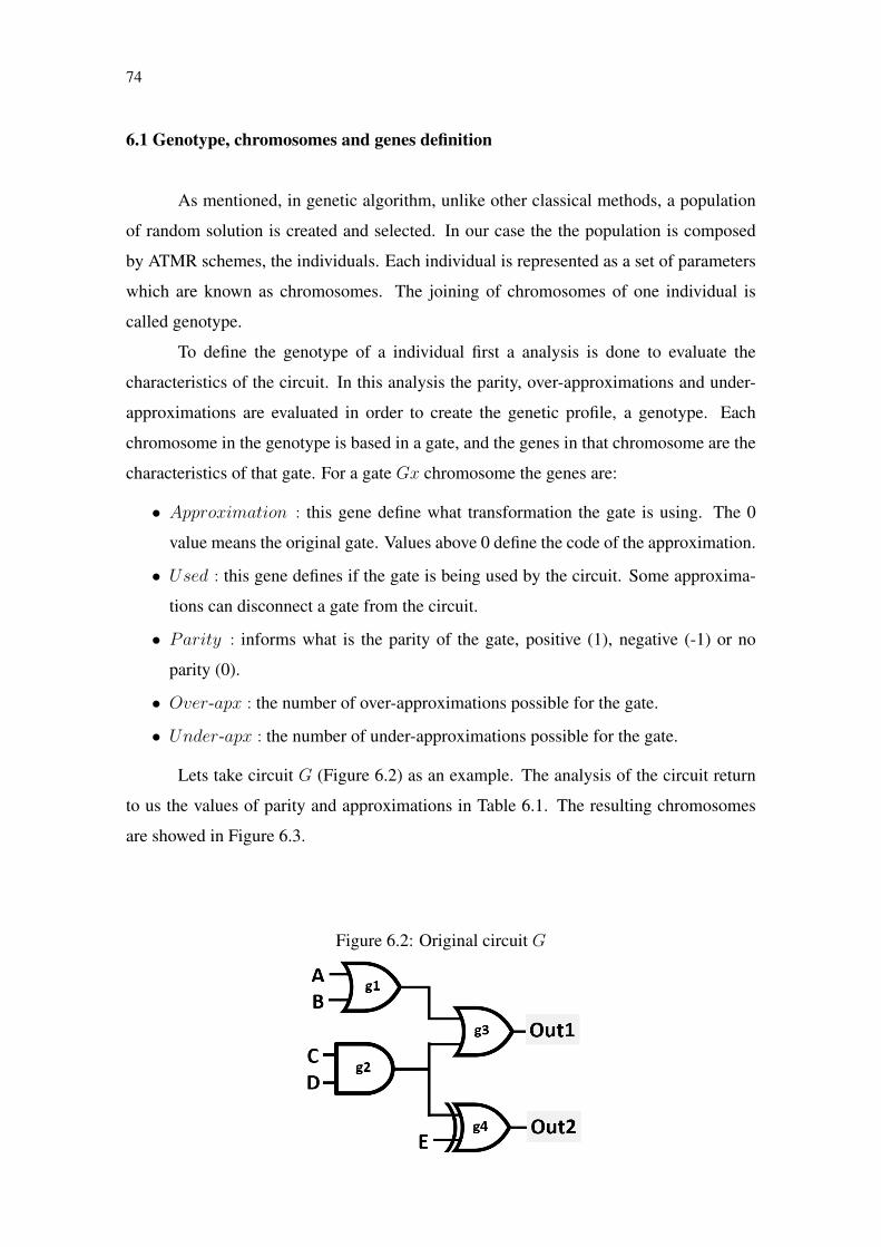
74
6.1 Genotype, chromosomes and genes definition
As mentioned, in genetic algorithm, unlike other classical methods, a population
of random solution is created and selected. In our case the the population is composed
by ATMR schemes, the individuals. Each individual is represented as a set of parameters
which are known as chromosomes. The joining of chromosomes of one individual is
called genotype.
To define the genotype of a individual first a analysis is done to evaluate the
characteristics of the circuit. In this analysis the parity, over-approximations and under-
approximations are evaluated in order to create the genetic profile, a genotype. Each
chromosome in the genotype is based in a gate, and the genes in that chromosome are the
characteristics of that gate. For a gate Gx chromosome the genes are:
• Approximation : this gene define what transformation the gate is using. The 0
value means the original gate. Values above 0 define the code of the approximation.
• Used : this gene defines if the gate is being used by the circuit. Some approxima-
tions can disconnect a gate from the circuit.
• Parity : informs what is the parity of the gate, positive (1), negative (-1) or no
parity (0).
• Over-apx : the number of over-approximations possible for the gate.
• Under-apx : the number of under-approximations possible for the gate.
Lets take circuit G (Figure 6.2) as an example. The analysis of the circuit return
to us the values of parity and approximations in Table 6.1. The resulting chromosomes
are showed in Figure 6.3.
Figure 6.2: Original circuit G

75
Table 6.1: Original circuit G genes evaluation.
Gate Under-apx Over-apx Parity
g1
Const-0 [cod : 1]
Line/Buffer (i1) [cod : 2]
Line/Buffer (i2) [cod : 3]
Const-1 [cod : 1]positive
(even)
g2 Const-0 [cod : 1]
Const-1 [cod : 1]
Line/Buffer (i1) [cod : 2]
Line/Buffer (i2) [cod : 3]
positive
(even)
g3
Const-0 [cod : 1]
Line/Buffer (i1) [cod : 2]
Line/Buffer (i2)[cod : 3]
Const-1 [cod : 1]binate
(no-parity)
g4
Const-0 [cod : 1]
NOi21 (v1) [cod : 2]
NOi21 (v2) [cod : 3]
Const-1 [cod : 1]
OR2 [cod : 2]
NAND2 [cod : 3]
positive
(even)
Figure 6.3: Original circuit G chromosomes.
The G circuit analysis generated four chromosomes, one for each gate in G. The
first chromosome represents the gate g1. Since it is the original circuit the approximation
gene is set to 0 and the used gene is set to true, meaning that the gate is in its original form
and is connected to the gates network. The parity gene is set to 1, meaning a positive
(even) parity. The over-apx gene indicates that there is just 1 possible transformation for
the gate g1, analogously, the under-apx is set to 3. The same process is done to the other
gates, generating their respective chromosomes and genes.
As seen before, a ATMR is composed by three circuits, G, F and H , and each
of these will have a chain of chromosomes to represent itself. Since G is the same for
every individual, the only information that we need to keep for a ATMR is the genotypes
for circuits F and H that compose it, i.e., each ATMR created will be represented by the
union of a Fx and Hx chromosomes.

76
6.2 Evolutionary operators
The evolutionary operators are responsible to improve the population by creat-
ing new individuals, selecting the best ones and combine then. There is three types of
evolutionary mechanisms: Mutation, Crossover and Selection.
6.2.1 Mutation mechanism
The mutation mechanism is applied to a individual in order to change some of
its genes. In our process the only gene to be mutated is the approximation. After the
mutation the genotype is processed, a circuit representation is created and then the parity
and used genes are reevaluated.
Lets try a example using the circuit in Figure 6.2. The original genotypes are
displayed in 6.3. The mutation process go through the chromosomes trying to create
first a over-approximated individual. At each one of the chromosomes it has a chance of
changing the approximation gene to a over-approximated gate. In this example, Figure
6.4a, the only mutation occurs in chromosome g4. The algorithm analysis the parity
of the chromosome, the value is 1, meaning a positive parity gate. To create a over-
approximation with a positive parity it must look at the value in gene over-apx, in this
case 3. Then the approximation gene change randomly to a value between 0 and 3. by
random chance value 2 is set at approximation gene. If the parity was negative (-1) the
algorithm would look in the under-apx to evaluate the values for approximations. If the
parity was 0, a binate gate, the mutation would be forbidden.
After the genotype is changed a circuit representation is generated, this represen-
tation is called phenotype. In our example the phenotype for the over-approximation is
represented in Figure 6.4b. The approach then reevaluates the genetic profile of the cir-
cuit, this time it verifies that gate g2 changed its parity from binate to a positive value,
therefore the chromosome representing this gate must also be changed (Figure 6.4c).
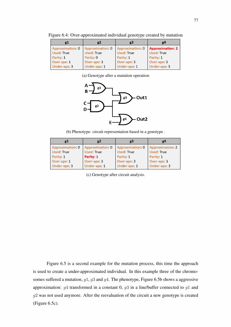
77
Figure 6.4: Over-approximated individual genotype created by mutation
(a) Genotype after a mutation operation
(b) Phenotype: circuit representation based in a genotype .
(c) Genotype after circuit analysis.
Figure 6.5 is a second example for the mutation process, this time the approach
is used to create a under-approximated individual. In this example three of the chromo-
somes suffered a mutation, g1, g3 and g4. The phenotype, Figure 6.5b shows a aggressive
approximation: g4 transformed in a constant 0, g3 in a line/buffer connected to g1 and
g2 was not used anymore. After the reevaluation of the circuit a new genotype is created
(Figure 6.5c).
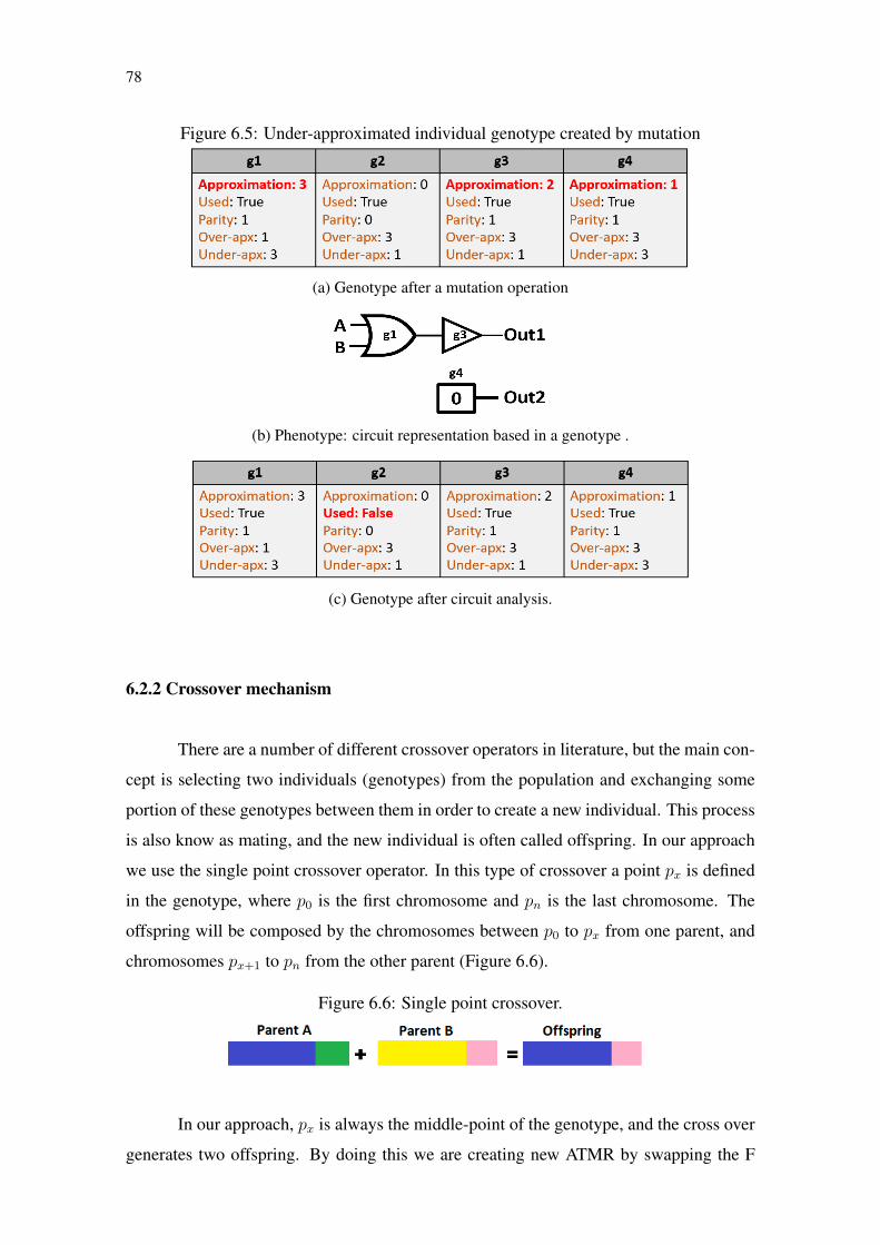
78
Figure 6.5: Under-approximated individual genotype created by mutation
(a) Genotype after a mutation operation
(b) Phenotype: circuit representation based in a genotype .
(c) Genotype after circuit analysis.
6.2.2 Crossover mechanism
There are a number of different crossover operators in literature, but the main con-
cept is selecting two individuals (genotypes) from the population and exchanging some
portion of these genotypes between them in order to create a new individual. This process
is also know as mating, and the new individual is often called offspring. In our approach
we use the single point crossover operator. In this type of crossover a point px is defined
in the genotype, where p0 is the first chromosome and pn is the last chromosome. The
offspring will be composed by the chromosomes between p0 to px from one parent, and
chromosomes px+1 to pn from the other parent (Figure 6.6).
Figure 6.6: Single point crossover.
In our approach, px is always the middle-point of the genotype, and the cross over
generates two offspring. By doing this we are creating new ATMR by swapping the F

79
and H modules between then. Lets see a example, Figure 6.7a is the original circuit G.
Figure 6.7a represents the complete G genotype. Figure 6.7c is a simplified genotype
form showing only the values for approximation genes of each gate.
Figure 6.7: Circuit G informations.
(a) Original circuit G.
(b) Genotype for circuit G.
(c) Simplified genotype for circuit G.
Or first parent for the crossover is ATMR1, composed by F1 and H1 circuits (Fig-
ure 6.8). The second parent for the crossover is ATMR2, composed by F2 and H2 cir-
cuits (Figure 6.9). Figure 6.10 shows the single point crossover operation, the first off-
spring, ATMR3, is composed by the under-approximated chromosomes of the first parent
(ATMR1), and the over-approximated chromosomes of the second parent (ATMR2). The
offspring ATMR3 ends being composed by the circuits F1 and H2.In a similar way the
second offspring, ATMR4, is composed by the under-chromosomes of ATMR2, and the
over-chromosomes of ATMR1, composing a new individual with circuits F2 and H1.

80
Figure 6.8: Circuit ATMR1 informations.
(a) Circuit F1.
(b) Circuit H1.
(c) Simplified genotype for ATMR1.
Figure 6.9: Circuit ATMR2 informations.
(a) Circuit F2. (b) Circuit H2.
(c) Simplified genotype for ATMR2.
Figure 6.10: Single point crossover example.

81
6.2.3 Selection mechanism
The selection is responsible for ranking the individuals in the population. The
solutions that are ranked best have a better chance to crossover and creating offspring,
while the worst ranked individual have less chance to mate with other individuals. The
main objective of selection operator is to keep and improve the individuals at each new
generation while keeping the size of the generation constant. Our approach uses a NSGA-
II (Non-dominated Sorting Genetic Algorithm II) to establish an order relationship among
the individuals of a population mainly based on te concept of non-dominance or Pareto
fronts (DEB et al., 2002).It is said that one solution Xi dominates other Xj if the first one
is better or equal than the second in every single objective and, at least, strictly better in
one of them (i.e. Pareto fronts are defined by those points in which no improvements in
one objective are possible without degrading the rest of objectives).
NSGA-II firstly groups individuals in a first front (F1) that contains all non-dominated
individuals, that is the Pareto front. Then, a second front (F2) is built by selecting all those
individuals that are non-dominated in the absence of individuals of the first front. This
process is repeated iteratively until all individuals are placed in some front. After the
fronts are built, NSGA-II gives another order for the individuals that belong to the same
front. To maintain a good spread of solutions, NSGA-II uses the crowding distance func-
tion (cd) to estimate the diversity value of a solution. Figure 6.11 illustrates a typical
pareto-front of a two objective minimizing optimization problem in solution space. The
grey are shows the whole population, while black line represents the best found individu-
als, the non-dominated ones. Summarizing, after the execution of the NSGA-II algorithm,
the population is first sorted by non-dominated fronts and then, by the crowding distance
(Figure 6.12).
Figure 6.11: Pareto-front of a Min–Min problem
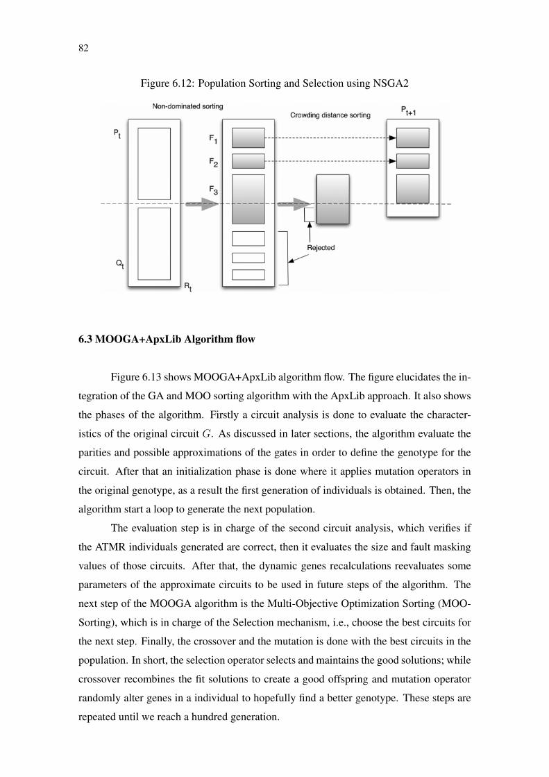
82
Figure 6.12: Population Sorting and Selection using NSGA2
6.3 MOOGA+ApxLib Algorithm flow
Figure 6.13 shows MOOGA+ApxLib algorithm flow. The figure elucidates the in-
tegration of the GA and MOO sorting algorithm with the ApxLib approach. It also shows
the phases of the algorithm. Firstly a circuit analysis is done to evaluate the character-
istics of the original circuit G. As discussed in later sections, the algorithm evaluate the
parities and possible approximations of the gates in order to define the genotype for the
circuit. After that an initialization phase is done where it applies mutation operators in
the original genotype, as a result the first generation of individuals is obtained. Then, the
algorithm start a loop to generate the next population.
The evaluation step is in charge of the second circuit analysis, which verifies if
the ATMR individuals generated are correct, then it evaluates the size and fault masking
values of those circuits. After that, the dynamic genes recalculations reevaluates some
parameters of the approximate circuits to be used in future steps of the algorithm. The
next step of the MOOGA algorithm is the Multi-Objective Optimization Sorting (MOO-
Sorting), which is in charge of the Selection mechanism, i.e., choose the best circuits for
the next step. Finally, the crossover and the mutation is done with the best circuits in the
population. In short, the selection operator selects and maintains the good solutions; while
crossover recombines the fit solutions to create a good offspring and mutation operator
randomly alter genes in a individual to hopefully find a better genotype. These steps are
repeated until we reach a hundred generation.
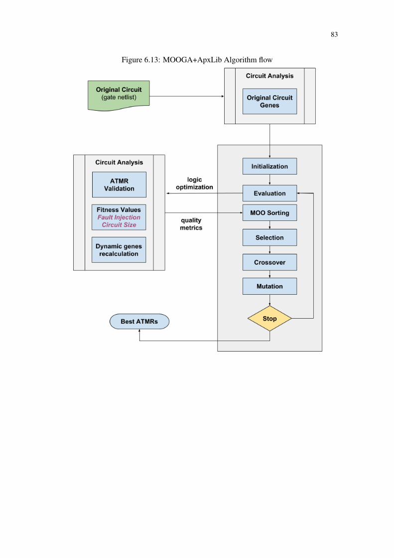
83
Figure 6.13: MOOGA+ApxLib Algorithm flow
84
6.4 Genetic approach results
The experiments were conducted a group of benchmarks extracted from LGSynth93
set: clpl, majority, cm82a, newtag and rd73. The original circuit for circuits clpl, newtag,
majority, cm82a, and rd73 were obtained using the academic logic synthesis tool ABC
using a custom standard cell library. Table 6.2 shows some information of the original
circuits synthesized.
Table 6.2: Benchmarks characteristicsBenchmark # gates #transistorsnewtag 7 34majority 6 36clpl 5 40cm82a 11 68rd73 21 142
Each resulting ATMR scheme has been evaluated in terms of error masking rate
by means of fault simulation. Due to the small size of considered benchmarks, an ex-
haustive analysis has been made, injecting faults in each gate output in the ATMR circuit
(excluding the voter) for every possible input vector. The results for fault injection were
done using a python simulator. The area overhead of the circuits is based in the number
of transistors of the ATMR circuit. The circuits benchmarks were evaluated setting up a
initial population of 10000 individuals, and for each new generation a 1000 new circuits
are created using mutation, crossover and selection approaches.
6.4.1 Population Analysis
Figures 6.14, 6.15, 6.16, 6.17, 6.18, shows all the individuals generated, also called
population, for circuits newtag, majority, clpl, cm82a and rd73 respectively. As we can
see, we have a large clouds of points, each point represents a individual ATMR circuit,
below that cloud is the pareto curve connecting the best circuits in the population. In
all the cases, both approximations have the same behavior, as the size overhead increase
the fault coverage increase too. This shows the correlation between the size and fault
coverage, objectives under evaluation.
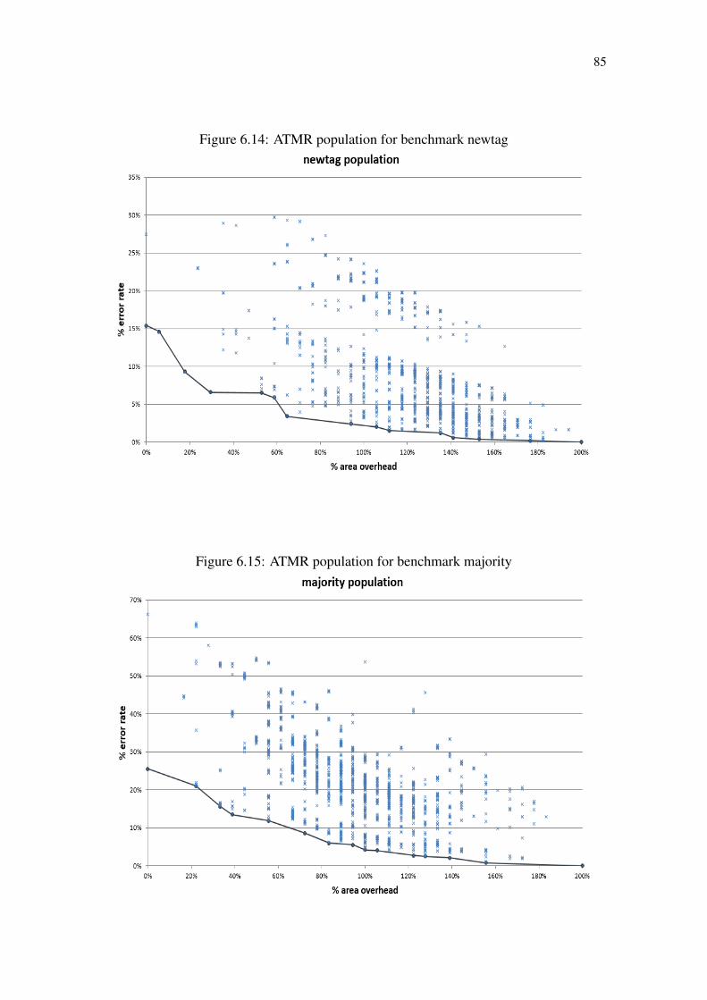
85
Figure 6.14: ATMR population for benchmark newtag
Figure 6.15: ATMR population for benchmark majority
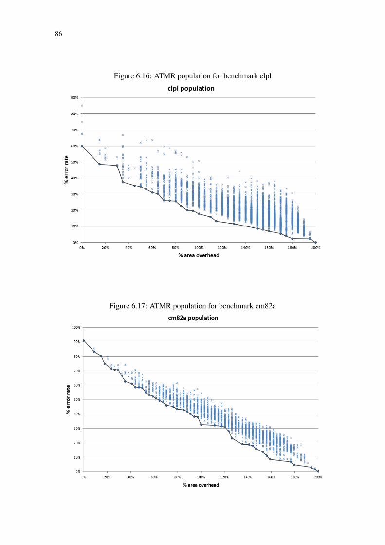
86
Figure 6.16: ATMR population for benchmark clpl
Figure 6.17: ATMR population for benchmark cm82a

87
Figure 6.18: ATMR population for benchmark rd73
Table 6.3 shows the number of ATMR circuits created for each benchmark. It is
possible to observe that there is no close correlation between the size of of the circuit,
number of gates, to the size of the population. Circuit rd73 has 21 gates and circuit
clpl has only 5 gates, however the size of the population for rd73 is almost the half of clpl
population. There is two reasons for that, first the number of possible transformations of a
given gate can range between 1 to 16, i.e, rd73 gates may have less possible approximation
options for each gate in its netlist compared to the gates that compose clpl. The second
answer is a little more complex, sometimes different genotypes can generate individuals
that represents the same logic function, therefore after the logic and mapping optimization
process both genotypes generate the same logic circuit.
Table 6.3: Population sizeBenchmark Population sizenewtag 1496majority 1840clpl 5540cm82a 1956rd73 2798
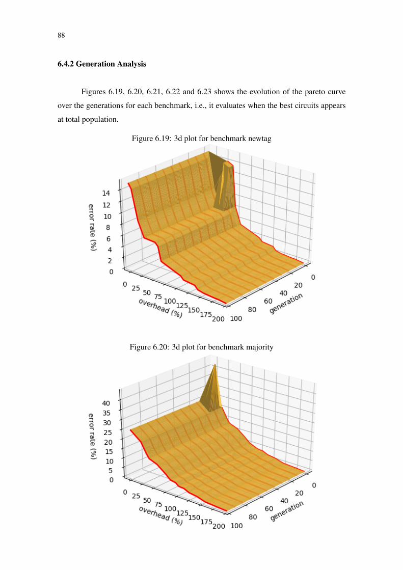
88
6.4.2 Generation Analysis
Figures 6.19, 6.20, 6.21, 6.22 and 6.23 shows the evolution of the pareto curve
over the generations for each benchmark, i.e., it evaluates when the best circuits appears
at total population.
Figure 6.19: 3d plot for benchmark newtag
Figure 6.20: 3d plot for benchmark majority
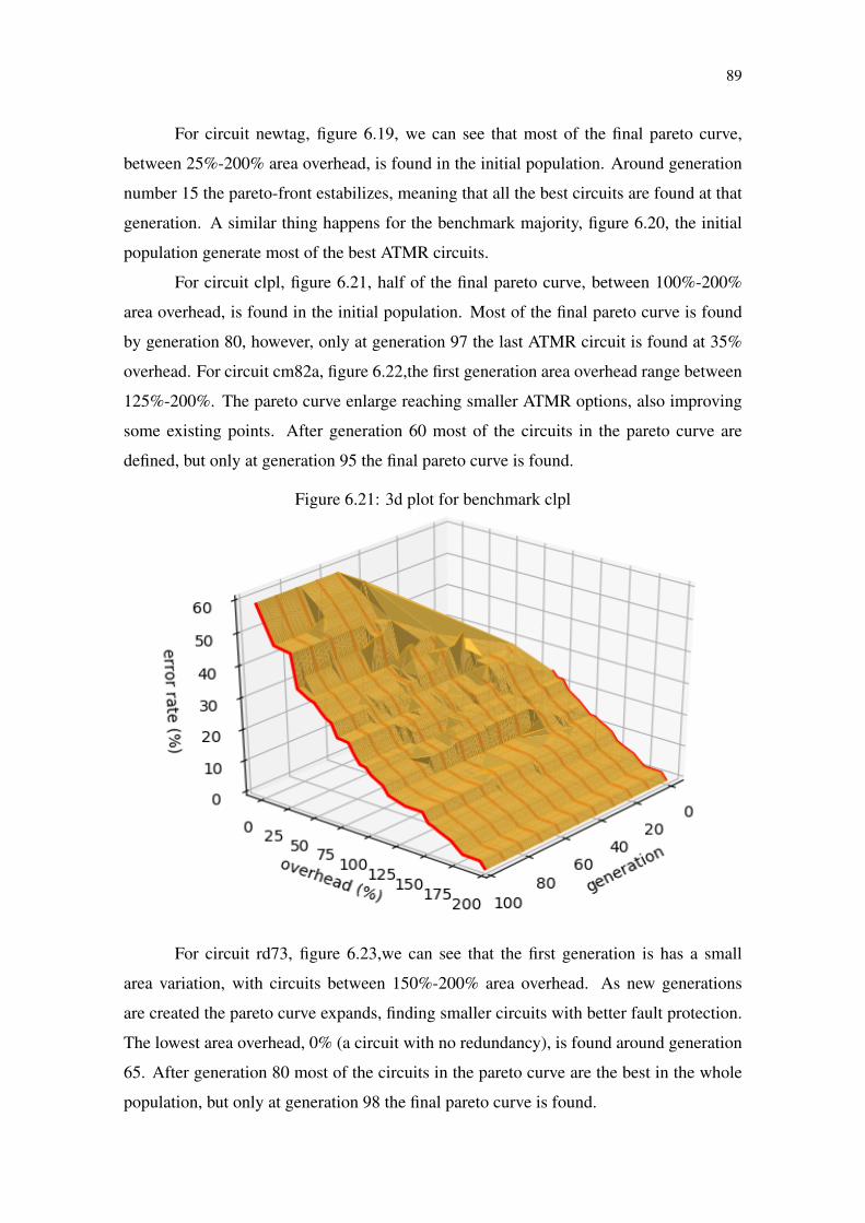
89
For circuit newtag, figure 6.19, we can see that most of the final pareto curve,
between 25%-200% area overhead, is found in the initial population. Around generation
number 15 the pareto-front estabilizes, meaning that all the best circuits are found at that
generation. A similar thing happens for the benchmark majority, figure 6.20, the initial
population generate most of the best ATMR circuits.
For circuit clpl, figure 6.21, half of the final pareto curve, between 100%-200%
area overhead, is found in the initial population. Most of the final pareto curve is found
by generation 80, however, only at generation 97 the last ATMR circuit is found at 35%
overhead. For circuit cm82a, figure 6.22,the first generation area overhead range between
125%-200%. The pareto curve enlarge reaching smaller ATMR options, also improving
some existing points. After generation 60 most of the circuits in the pareto curve are
defined, but only at generation 95 the final pareto curve is found.
Figure 6.21: 3d plot for benchmark clpl
For circuit rd73, figure 6.23,we can see that the first generation is has a small
area variation, with circuits between 150%-200% area overhead. As new generations
are created the pareto curve expands, finding smaller circuits with better fault protection.
The lowest area overhead, 0% (a circuit with no redundancy), is found around generation
65. After generation 80 most of the circuits in the pareto curve are the best in the whole
population, but only at generation 98 the final pareto curve is found.
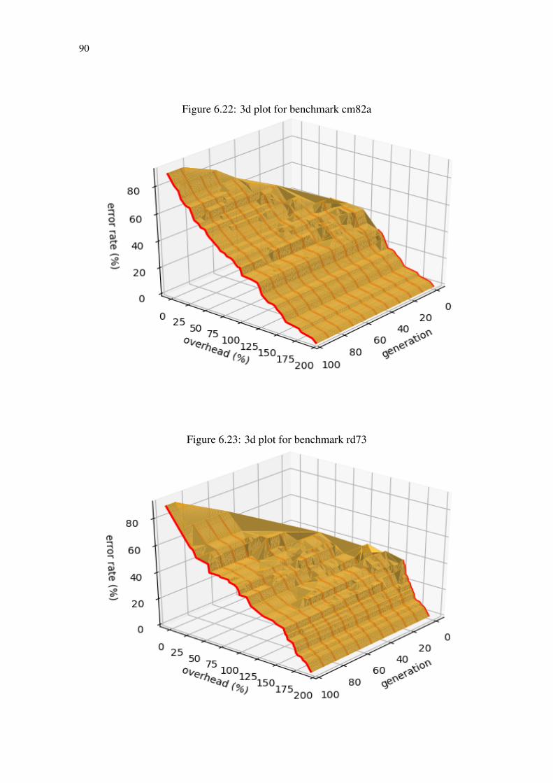
90
Figure 6.22: 3d plot for benchmark cm82a
Figure 6.23: 3d plot for benchmark rd73
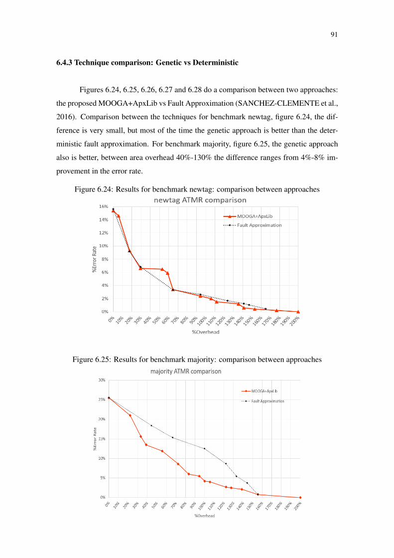
91
6.4.3 Technique comparison: Genetic vs Deterministic
Figures 6.24, 6.25, 6.26, 6.27 and 6.28 do a comparison between two approaches:
the proposed MOOGA+ApxLib vs Fault Approximation (SANCHEZ-CLEMENTE et al.,
2016). Comparison between the techniques for benchmark newtag, figure 6.24, the dif-
ference is very small, but most of the time the genetic approach is better than the deter-
ministic fault approximation. For benchmark majority, figure 6.25, the genetic approach
also is better, between area overhead 40%-130% the difference ranges from 4%-8% im-
provement in the error rate.
Figure 6.24: Results for benchmark newtag: comparison between approaches
Figure 6.25: Results for benchmark majority: comparison between approaches
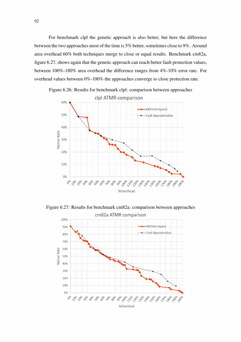
92
For benchmark clpl the genetic approach is also better, but here the difference
between the two approaches most of the time is 5% better, sometimes close to 9%. Around
area overhead 60% both techniques merge to close or equal results. Benchmark cm82a,
figure 6.27, shows again that the genetic approach can reach better fault protection values,
between 100%-180% area overhead the difference ranges from 4%-10% error rate. For
overhead values between 0%-100% the approaches converge to close protection rate.
Figure 6.26: Results for benchmark clpl: comparison between approaches
Figure 6.27: Results for benchmark cm82a: comparison between approaches
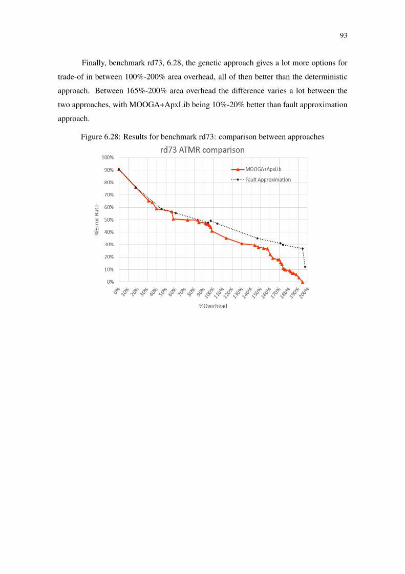
93
Finally, benchmark rd73, 6.28, the genetic approach gives a lot more options for
trade-of in between 100%-200% area overhead, all of then better than the deterministic
approach. Between 165%-200% area overhead the difference varies a lot between the
two approaches, with MOOGA+ApxLib being 10%-20% better than fault approximation
approach.
Figure 6.28: Results for benchmark rd73: comparison between approaches
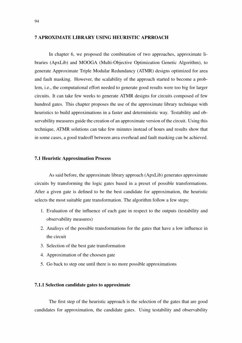
94
7 APROXIMATE LIBRARY USING HEURISTIC APRROACH
In chapter 6, we proposed the combination of two approaches, approximate li-
braries (ApxLib) and MOOGA (Multi-Objective Optimization Genetic Algorithm), to
generate Approximate Triple Modular Redundancy (ATMR) designs optimized for area
and fault masking. However, the scalability of the approach started to become a prob-
lem, i.e., the computational effort needed to generate good results were too big for larger
circuits. It can take few weeks to generate ATMR designs for circuits composed of few
hundred gates. This chapter proposes the use of the approximate library technique with
heuristics to build approximations in a faster and deterministic way. Testability and ob-
servability measures guide the creation of an approximate version of the circuit. Using this
technique, ATMR solutions can take few minutes instead of hours and results show that
in some cases, a good tradeoff between area overhead and fault masking can be achieved.
7.1 Heuristic Approximation Process
As said before, the approximate library approach (ApxLib) generates approximate
circuits by transforming the logic gates based in a preset of possible transformations.
After a given gate is defined to be the best candidate for approximation, the heuristic
selects the most suitable gate transformation. The algorithm follow a few steps:
1. Evaluation of the influence of each gate in respect to the outputs (testability and
observability measures)
2. Analisys of the possible transformations for the gates that have a low influence in
the circuit
3. Selection of the best gate transformation
4. Approximation of the choosen gate
5. Go back to step one until there is no more possible approximations
7.1.1 Selection candidate gates to approximate
The first step of the heuristic approach is the selection of the gates that are good
candidates for approximation, the candidate gates. Using testability and observability
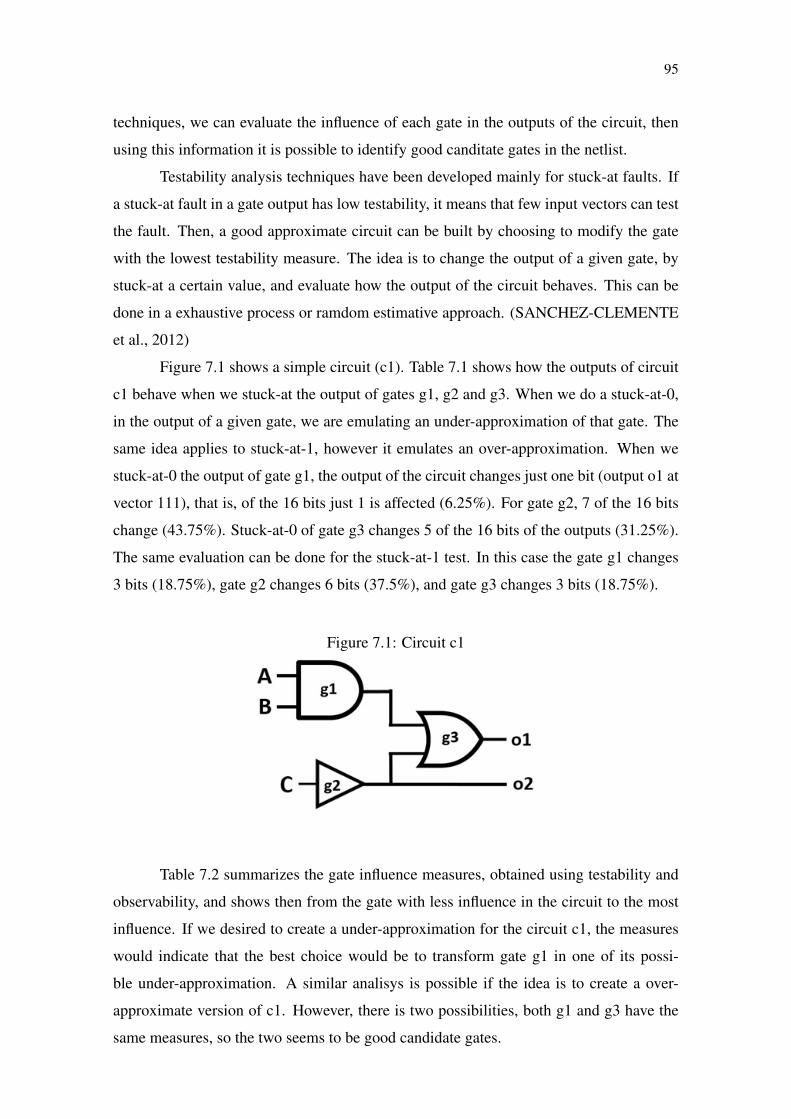
95
techniques, we can evaluate the influence of each gate in the outputs of the circuit, then
using this information it is possible to identify good canditate gates in the netlist.
Testability analysis techniques have been developed mainly for stuck-at faults. If
a stuck-at fault in a gate output has low testability, it means that few input vectors can test
the fault. Then, a good approximate circuit can be built by choosing to modify the gate
with the lowest testability measure. The idea is to change the output of a given gate, by
stuck-at a certain value, and evaluate how the output of the circuit behaves. This can be
done in a exhaustive process or ramdom estimative approach. (SANCHEZ-CLEMENTE
et al., 2012)
Figure 7.1 shows a simple circuit (c1). Table 7.1 shows how the outputs of circuit
c1 behave when we stuck-at the output of gates g1, g2 and g3. When we do a stuck-at-0,
in the output of a given gate, we are emulating an under-approximation of that gate. The
same idea applies to stuck-at-1, however it emulates an over-approximation. When we
stuck-at-0 the output of gate g1, the output of the circuit changes just one bit (output o1 at
vector 111), that is, of the 16 bits just 1 is affected (6.25%). For gate g2, 7 of the 16 bits
change (43.75%). Stuck-at-0 of gate g3 changes 5 of the 16 bits of the outputs (31.25%).
The same evaluation can be done for the stuck-at-1 test. In this case the gate g1 changes
3 bits (18.75%), gate g2 changes 6 bits (37.5%), and gate g3 changes 3 bits (18.75%).
Figure 7.1: Circuit c1
Table 7.2 summarizes the gate influence measures, obtained using testability and
observability, and shows then from the gate with less influence in the circuit to the most
influence. If we desired to create a under-approximation for the circuit c1, the measures
would indicate that the best choice would be to transform gate g1 in one of its possi-
ble under-approximation. A similar analisys is possible if the idea is to create a over-
approximate version of c1. However, there is two possibilities, both g1 and g3 have the
same measures, so the two seems to be good candidate gates.
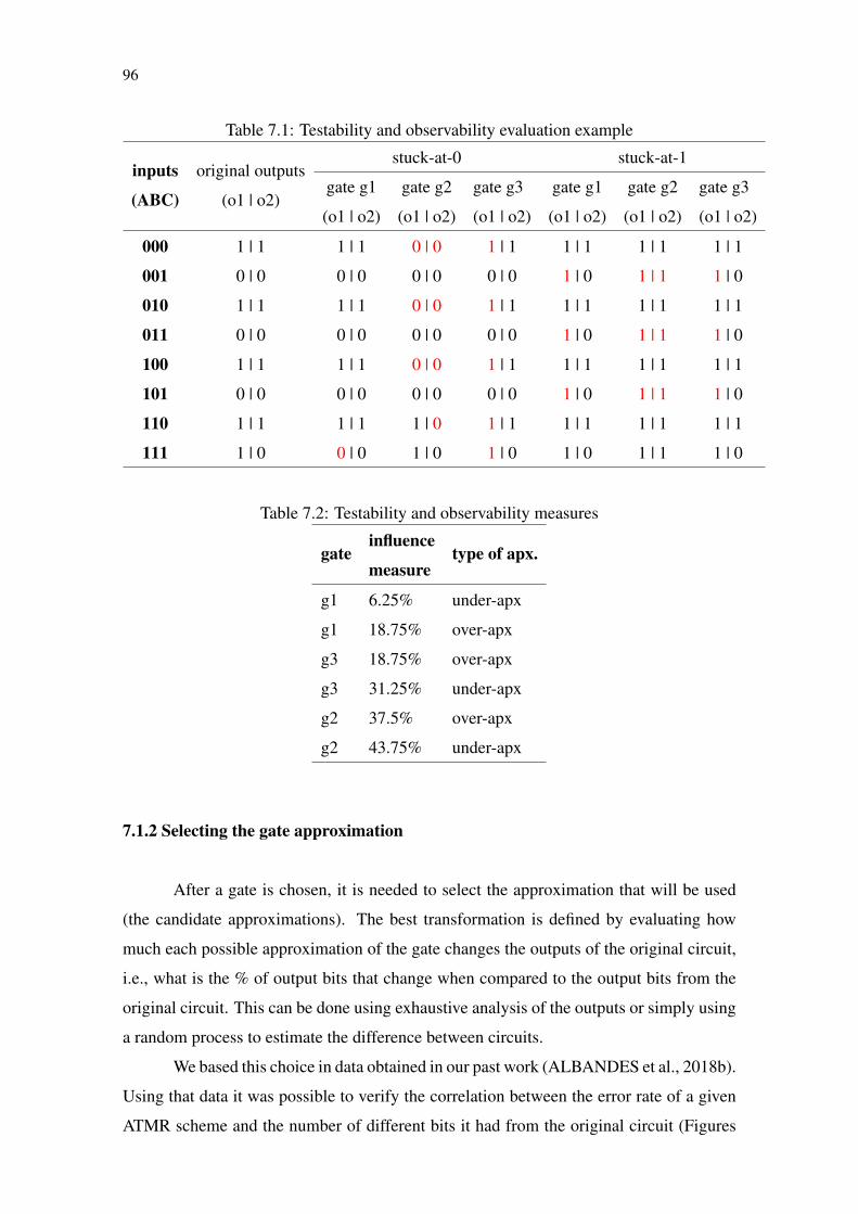
96
Table 7.1: Testability and observability evaluation example
stuck-at-0 stuck-at-1inputs
(ABC)
original outputs
(o1 | o2)gate g1
(o1 | o2)
gate g2
(o1 | o2)
gate g3
(o1 | o2)
gate g1
(o1 | o2)
gate g2
(o1 | o2)
gate g3
(o1 | o2)
000 1 | 1 1 | 1 0 | 0 1 | 1 1 | 1 1 | 1 1 | 1
001 0 | 0 0 | 0 0 | 0 0 | 0 1 | 0 1 | 1 1 | 0
010 1 | 1 1 | 1 0 | 0 1 | 1 1 | 1 1 | 1 1 | 1
011 0 | 0 0 | 0 0 | 0 0 | 0 1 | 0 1 | 1 1 | 0
100 1 | 1 1 | 1 0 | 0 1 | 1 1 | 1 1 | 1 1 | 1
101 0 | 0 0 | 0 0 | 0 0 | 0 1 | 0 1 | 1 1 | 0
110 1 | 1 1 | 1 1 | 0 1 | 1 1 | 1 1 | 1 1 | 1
111 1 | 0 0 | 0 1 | 0 1 | 0 1 | 0 1 | 1 1 | 0
Table 7.2: Testability and observability measures
gateinfluence
measuretype of apx.
g1 6.25% under-apx
g1 18.75% over-apx
g3 18.75% over-apx
g3 31.25% under-apx
g2 37.5% over-apx
g2 43.75% under-apx
7.1.2 Selecting the gate approximation
After a gate is chosen, it is needed to select the approximation that will be used
(the candidate approximations). The best transformation is defined by evaluating how
much each possible approximation of the gate changes the outputs of the original circuit,
i.e., what is the % of output bits that change when compared to the output bits from the
original circuit. This can be done using exhaustive analysis of the outputs or simply using
a random process to estimate the difference between circuits.
We based this choice in data obtained in our past work (ALBANDES et al., 2018b).
Using that data it was possible to verify the correlation between the error rate of a given
ATMR scheme and the number of different bits it had from the original circuit (Figures

97
7.2, 7.3, 7.4 and 7.5). Table 7.3 shows the correlation values obtained with past data. The
data showed that there is a strong correlation between the two parameters, i.e., when the
ATMR circuits has a high difference of bits between the original circuit and the approxi-
mate modules the error rate also will be higher.
Figure 7.2: Correlation graph for benchmark majority
Figure 7.3: Correlation graph for benchmark newtag
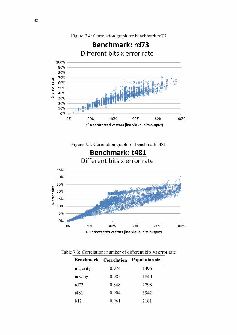
98
Figure 7.4: Correlation graph for benchmark rd73
Figure 7.5: Correlation graph for benchmark t481
Table 7.3: Correlation: number of different bits vs error rate
Benchmark Correlation Population size
majority 0.974 1496
newtag 0.985 1840
rd73 0.848 2798
t481 0.904 3942
b12 0.961 2181
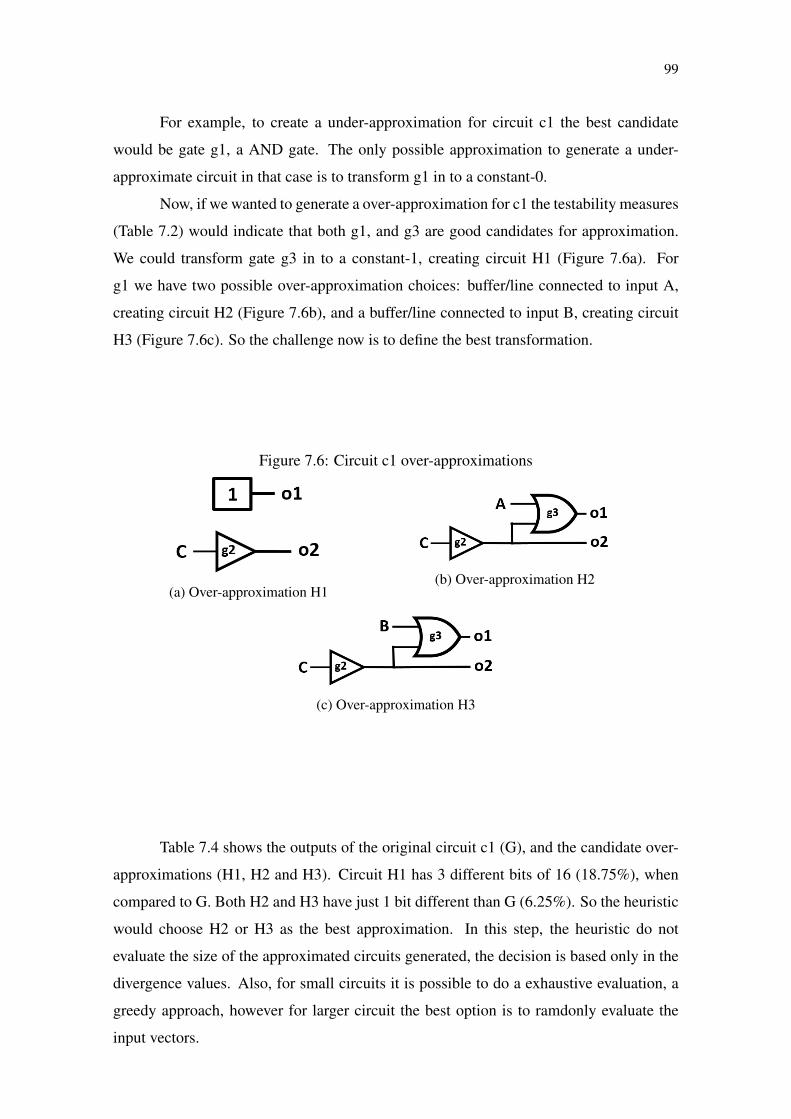
99
For example, to create a under-approximation for circuit c1 the best candidate
would be gate g1, a AND gate. The only possible approximation to generate a under-
approximate circuit in that case is to transform g1 in to a constant-0.
Now, if we wanted to generate a over-approximation for c1 the testability measures
(Table 7.2) would indicate that both g1, and g3 are good candidates for approximation.
We could transform gate g3 in to a constant-1, creating circuit H1 (Figure 7.6a). For
g1 we have two possible over-approximation choices: buffer/line connected to input A,
creating circuit H2 (Figure 7.6b), and a buffer/line connected to input B, creating circuit
H3 (Figure 7.6c). So the challenge now is to define the best transformation.
Figure 7.6: Circuit c1 over-approximations
(a) Over-approximation H1(b) Over-approximation H2
(c) Over-approximation H3
Table 7.4 shows the outputs of the original circuit c1 (G), and the candidate over-
approximations (H1, H2 and H3). Circuit H1 has 3 different bits of 16 (18.75%), when
compared to G. Both H2 and H3 have just 1 bit different than G (6.25%). So the heuristic
would choose H2 or H3 as the best approximation. In this step, the heuristic do not
evaluate the size of the approximated circuits generated, the decision is based only in the
divergence values. Also, for small circuits it is possible to do a exhaustive evaluation, a
greedy approach, however for larger circuit the best option is to ramdonly evaluate the
input vectors.
100
Table 7.4: Truth table of candidate approximations
Input
(ABC)
G
(o1 |o2)
H1
(o1 |o2)
H2
(o1 |o2)
H3
(o1 |o2)
000 1 | 1 1 | 1 1 | 1 1 | 1
001 0 | 0 1 | 1 0 | 0 0 | 0
010 1 | 1 1 | 1 1 | 1 1 | 1
011 0 | 0 1 | 0 0 | 0 1 | 0
100 1 | 1 1 | 1 1 | 1 1 | 1
101 0 | 0 1 | 1 1 | 1 0 | 0
110 1 | 1 1 | 1 1 | 1 1 | 1
111 1 | 0 1 | 0 1 | 0 1 | 0
7.1.3 Iteration process
We can simplify the heuristic process by separating it in three steps: 1. candidate
gates evaluation; 2. candidate approximations evaluation; 3. heuristic selection of best
approximation based in steps 1 and 2; And then the process repeat itself until necessary.
After this process is done the algorithm will generate dozens of approximate circuits,
which will then be logicaly optimized and synthesized using a cell library. After the
circuits were synthesized the fault injection is done in order to evaluate error rate of the
ATMR circuits created.
Figure 7.7 elucidates the algorithm flow used for small benchmark circuits. In this
process each iteration cycle repeats the testability and observability step, creating a new
measure table after each new approximation is created, which can be very time consuming
for large circuits. Also, this process creates under and over approximations separatedly,
and in later stages it permutates F and H circuits to build ATMR designs. For example, for
a circuit that generated just 20 under-approximations and another 40 over approximations,
would generate 800 ATMR designs.

101
Figure 7.7: Heuristic approach 1 flowchart (small circuits)
Figure 7.8 elucidates the algorithm flow used for larger benchmark circuits. The
first modification is related to the testability and observability measures, here the mea-
surement is done only after a certain number of gates were approximated or if all the
initial gates measures are already used to evaluate the candidates. Also, the F and H cir-
cuits were created together, i.e, each approximation generates a complete ATMR design,
so there is no permutation process in the end.
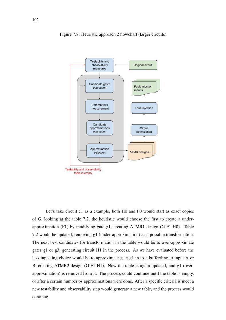
102
Figure 7.8: Heuristic approach 2 flowchart (larger circuits)
Let’s take circuit c1 as a example, both H0 and F0 would start as exact copies
of G, looking at the table 7.2, the heuristic would choose the first to create a under-
approximation (F1) by modifying gate g1, creating ATMR1 design (G-F1-H0). Table
7.2 would be updated, removing g1 (under-approximation) as a possible transformation.
The next best candidates for transformation in the table would be to over-approximate
gates g1 or g3, generating circuit H1 in the process. As we have evaluated before the
less inpacting choice would be to approximate gate g1 in to a buffer/line to input A or
B, creating ATMR2 design (G-F1-H1). Now the table is again updated, and g1 (over-
approximation) is removed from it. The process could continue until the table is empty,
or after a certain number os approximations were done. After a specific criteria is meet a
new testability and observability step would generate a new table, and the process would
continue.

103
7.2 Apxlib+Heuristic approach results
The experiments were conducted a group of benchmarks extracted from LGSynth93
set: clpl, newtag and rd73. The original circuit for circuits clpl, newtag and rd73 were
obtained using the academic logic synthesis tool ABC (BRAYTON; MISHCHENKO,
2010) using a custom standard cell library. Table A.10 shows some information of the
original circuits synthesized. Table A.11 shows information about the execution time for
both techniques, comparing the computational effort between the two approaches. The
heuristic approach 1, for small circuits (figure 7.7), was used for the results.
Table 7.5: Benchmarks characteristicsBenchmark #inputs #outputs #gates #transistorsmajority 5 1 6 36clpl 11 5 5 40cm82a 5 3 11 68rd73 7 3 21 142
Table 7.6: Execution time: MOOGA vs Heuristic
BenchmarksExecution Time
ApxLib+MOOGA ApxLib+Heuristic
majority ∼1h30m ∼1min
clpl ∼1h30m ∼1min
cm82a ∼1h30m ∼1min
Rd73 ∼3h30m ∼1min
Each resulting ATMR scheme has been evaluated regarding error masking rate
using fault simulation. Due to the small size of considered benchmarks, an exhaustive
analysis has been made, injecting faults in the output of each gate in the ATMR circuit
(excluding the voter) for every possible input vector.For the heuristic approach, both the
testability measures and the calculation of different bits used an exhaustive analysis, also
due to the small size of the circuits.
The results for fault injection were done using a custom-made python simulator.
The area overhead of the circuits is based on the number of transistors of the ATMR
circuit. The whole ApxLib+MOOGA process takes hours to generate the final results.
The deterministic approach, ApxLib+Heuristic, usually takes around a minute to generate
and evaluate the ATMR circuits.
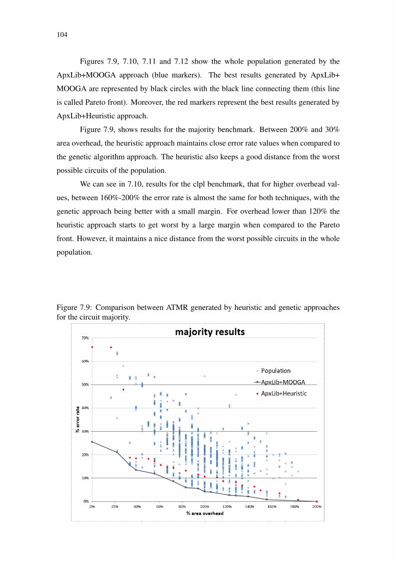
104
Figures 7.9, 7.10, 7.11 and 7.12 show the whole population generated by the
ApxLib+MOOGA approach (blue markers). The best results generated by ApxLib+
MOOGA are represented by black circles with the black line connecting them (this line
is called Pareto front). Moreover, the red markers represent the best results generated by
ApxLib+Heuristic approach.
Figure 7.9, shows results for the majority benchmark. Between 200% and 30%
area overhead, the heuristic approach maintains close error rate values when compared to
the genetic algorithm approach. The heuristic also keeps a good distance from the worst
possible circuits of the population.
We can see in 7.10, results for the clpl benchmark, that for higher overhead val-
ues, between 160%-200% the error rate is almost the same for both techniques, with the
genetic approach being better with a small margin. For overhead lower than 120% the
heuristic approach starts to get worst by a large margin when compared to the Pareto
front. However, it maintains a nice distance from the worst possible circuits in the whole
population.
Figure 7.9: Comparison between ATMR generated by heuristic and genetic approachesfor the circuit majority.
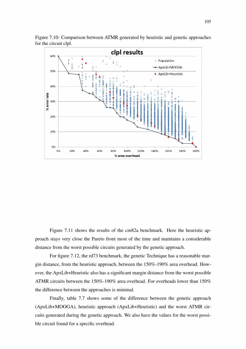
105
Figure 7.10: Comparison between ATMR generated by heuristic and genetic approachesfor the circuit clpl.
Figure 7.11 shows the results of the cm82a benchmark. Here the heuristic ap-
proach stays very close the Pareto front most of the time and maintains a considerable
distance from the worst possible circuits generated by the genetic approach.
For figure 7.12, the rd73 benchmark, the genetic Technique has a reasonable mar-
gin distance, from the heuristic approach, between the 150%-190% area overhead. How-
ever, the ApxLib+Heuristic also has a significant margin distance from the worst possible
ATMR circuits between the 150%-190% area overhead. For overheads lower than 150%
the difference between the approaches is minimal.
Finally, table 7.7 shows some of the difference between the genetic approach
(ApxLib+MOOGA), heuristic approach (ApxLib+Heuristic) and the worst ATMR cir-
cuits generated during the genetic approach. We also have the values for the worst possi-
ble circuit found for a specific overhead.
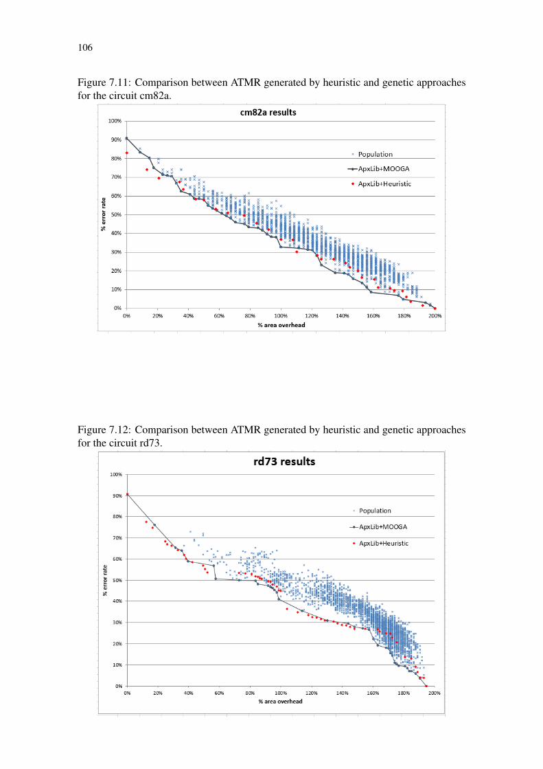
106
Figure 7.11: Comparison between ATMR generated by heuristic and genetic approachesfor the circuit cm82a.
Figure 7.12: Comparison between ATMR generated by heuristic and genetic approachesfor the circuit rd73.
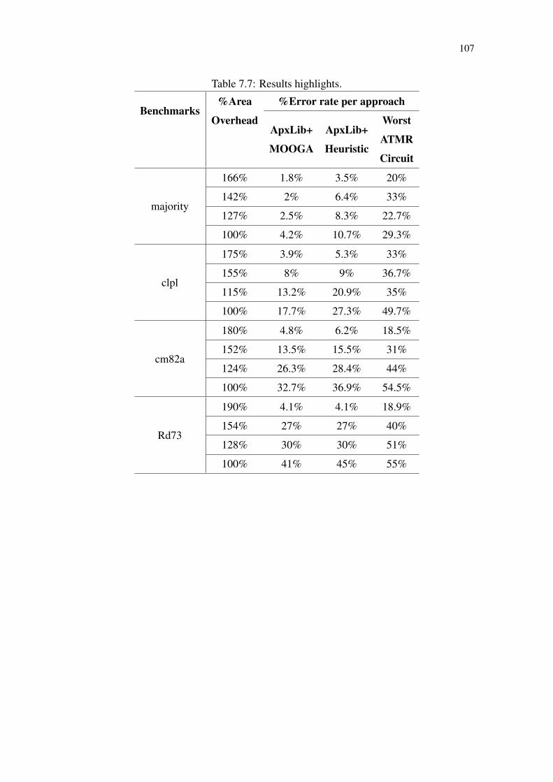
107
Table 7.7: Results highlights.
Benchmarks%Area
Overhead
%Error rate per approach
ApxLib+
MOOGA
ApxLib+
Heuristic
Worst
ATMR
Circuit
majority
166% 1.8% 3.5% 20%
142% 2% 6.4% 33%
127% 2.5% 8.3% 22.7%
100% 4.2% 10.7% 29.3%
clpl
175% 3.9% 5.3% 33%
155% 8% 9% 36.7%
115% 13.2% 20.9% 35%
100% 17.7% 27.3% 49.7%
cm82a
180% 4.8% 6.2% 18.5%
152% 13.5% 15.5% 31%
124% 26.3% 28.4% 44%
100% 32.7% 36.9% 54.5%
Rd73
190% 4.1% 4.1% 18.9%
154% 27% 27% 40%
128% 30% 30% 51%
100% 41% 45% 55%

108
8 CONCLUSION
Technology scaling poses an increasing challenge to hardware reliability. Circuits
manufactured on advanced technologies are more susceptible to errors, mainly as a con-
sequence of the shrinking of transistor dimensions and the increased integration density.
Fault mitigation techniques able to mask soft errors require redundancy and major-
ity voters. Triple Modular Redundancy (TMR) is a well-known technique, which provides
excellent concurrent masking capability. However, these techniques introduce consider-
able overheads regarding both area and power consumption, higher than 200%. Alterna-
tively, partial redundancy is often sought to find a good balance between the reliability
requirements and the area, power and performance requirements.
Within this context, approximate circuits have recently emerged as an alternative
approach for building partial TMR solutions. An approximate logic circuit is a circuit that
performs a different but closely related logic function to the original circuit. As it is not
required to match the original circuit exactly, the approximate circuit can be smaller, but it
can still be used as replicas in the TMR to be voted at the majority voter and consequently
mask faults. We call this Approximate-TMR (ATMR).
This work proposed three novel approaches to design ATMR circuits. The first
is the concept of Full-ATMR (FATMR), a design were all modules of the TMR are ap-
proximated. Full-ATMR allows for a greater reduction of overhead costs and still can
maintain a good protection ratio. It was possible to keep the protected p-n junction ratio
above 97% with only 125% area overhead. For the ATMR version of a 4-bit ripple-carry
adder, several implementations are proposed, ranging from 93%-136% to 96%-168% of
protected junctions and area overhead, respectively.
The second approach was a combination of the Approximate Library with Multi-
Objective Optimization Genetic Algorithm (ApxLib+MOOGA). The approach was com-
pared to the a sate-of-the-art technique (fault approximation). The approach showed good
balance between the reliability requirements and the area, in general ApxLib+MOOGA
presented better results than the fault approximation method. However the ApxLib+MOOGA
was to time consuming, even for small circuits.
The third and last approach is a combination of the Approximate Library with
Heuristic (ApxLib+Heuristic). This new approach was compared to ApxLib+MOOGA
regarding the circuits created and the execution time to do it. The heuristic approach
(ApxLib+Heuristic) shows good balance between the reliability requirements and the
109
area, while it maintains a low computational effort when compared to the genetic tech-
nique (ApxLib+MOOGA), taking around a minute instead of hours to generate the results.
We could also see that even when it is far from the Pareto front, the ApxLib+Heuristic
approach still has a good advantage over the worst possible solutions for all the tested
benchmarks. Likely these promising results could be improved by making a few changes
in the algorithm heuristics and later apply the technique to larger circuits. Also it would
be interesting to adapt the approach to use in FPGAs.This research generated four publications (ALBANDES et al., 2015b), (ALBAN-
DES et al., 2015a), (ALBANDES et al., 2018b) and (ALBANDES et al., 2018a).

110
REFERENCES
ALBANDES, I.; KASTENSMIDT, F. Methodology for achieving best trade-off ofarea and fault masking coverage in atmr. IEEE Latin-American Test Workshop(LATW2014), p. 1–6, 2014.
ALBANDES, I. et al. Reducing tmr overhead by combining approximate circuit,transistor topology and input permutation approaches. SYMPOSIUM ONINTEGRATED CIRCUITS AND SYSTEMS DESIGN (SBCCI), p. 1–6, 2013.
ALBANDES, I. et al. Exploring the use of approximate tmr to mask transient faults inlogic with low area overhead. Microelectronics Reliability, v. 55, n. 9-10, p. 2072–2076,2015.
ALBANDES, I. et al. Using only redundant modules with approximate logic to reducedrastically area overhead in tmr. 2015 16th Latin-American Test Symposium (LATS),p. 1–6, 2015.
ALBANDES, I. et al. Design of approximate-tmr using approximate library and heuristicapproaches. Microelectronics Reliability, p. 1–6, 2018.
ALBANDES, I. et al. Improving approximate-tmr using multi-objective optimizationgenetic algorithm. 2018 19th Latin-American Test Symposium (LATS), p. 1–6, 2018.
AMOUZGAR, K. Multi-Objective Optimization using Genetic Algorithms. [S.l.]:Dissertation - School of Engineering, Jönköping University, 2012.
ARTOLA, L.; HUBERT, G.; SCHRIMPF, R. D. Modeling of radiation-induced singleevent transients in soi finfets. In: 2013 IEEE International Reliability PhysicsSymposium (IRPS). [S.l.: s.n.], 2013. p. SE.1.1–SE.1.6.
BAUMANN, R. C. Radiation-induced soft errors in advanced semiconductortechnologies. Device and Materials Reliability, v. 5, n. 3, p. 305–316, 2005.
BRAYTON, R.; MISHCHENKO, A. Abc: An academic industrial-strength verificationtool. Computer Aided Verification, v. 6174, 2010.
CHOUDHURY, M. R.; MOHANRAM, K. Low cost concurrent error masking usingapproximate logic circuits. IEEE Transactions on Computer-Aided Design ofIntegrated Circuits and Systems, v. 32, n. 8, p. 1163–1176, Aug 2013.
DEB, K. et al. A fast and elitist multiobjective genetic algorithm: Nsga-ii. IEEETransactions on Evolutionary Computation, v. 6, n. 2, p. 182–197, Apr 2002.
DODD, P. E.; MASSENGILL, L. W. Basic mechanisms and modeling of single-eventupset in digital microelectronics. IEEE Transactions on Nuclear Science, v. 50, n. 3, p.583–602, June 2003.
DYER, C. et al. Extreme atmospheric radiation environments and single event effects.IEEE Transactions on Nuclear Science, PP, n. 99, p. 1–1, 2017.
EL-MAMOUNI, F. et al. Laser- and heavy ion-induced charge collection in bulk finfets.IEEE Transactions on Nuclear Science, v. 58, n. 6, p. 2563–2569, Dec 2011.

111
ENTRENA, L. et al. Logic optimization of unidirectional circuits with structuralmethods. In: Proceedings Seventh International On-Line Testing Workshop. [S.l.:s.n.], 2001. p. 43–47.
GADLAGE, M. J. et al. Single event transient pulse widths in digital microcircuits.IEEE Transactions on Nuclear Science, v. 51, n. 6, p. 3285–3290, Dec 2004.
GARGINI, P. A. How to successfully overcome inflection points, or long live moore’slaw. Computing in Science Engineering, v. 19, n. 2, p. 51–62, Mar 2017.
GUARNIERI, M. The unreasonable accuracy of moore’s law [historical]. IEEEIndustrial Electronics Magazine, v. 10, n. 1, p. 40–43, March 2016.
LEE, T. L.; WANG, C. Y. Recognition of fanout-free functions. In: 2007 Asia and SouthPacific Design Automation Conference. [S.l.: s.n.], 2007. p. 426–431.
MARTINELLO, O. et al. Kl-cuts: A new approach for logic synthesis targeting multipleoutput blocks. In: 2010 Design, Automation Test in Europe Conference Exhibition(DATE 2010). [S.l.: s.n.], 2010. p. 777–782.
MARTINS, M. G. A.; RIBAS, R. P.; REIS, A. I. Functional composition: A newparadigm for performing logic synthesis. In: Thirteenth International Symposium onQuality Electronic Design (ISQED). [S.l.: s.n.], 2012. p. 236–242.
MARTINS, M. G. A. et al. Boolean factoring with multi-objective goals. In: 2010 IEEEInternational Conference on Computer Design. [S.l.: s.n.], 2010. p. 229–234.
MOORE, G. E. Cramming more components onto integrated circuits, reprinted fromelectronics, volume 38, number 8, april 19, 1965, pp.114 ff. IEEE Solid-State CircuitsSociety Newsletter, v. 11, n. 3, p. 33–35, 2006.
MUNTEANU, D.; AUTRAN, J. L. Modeling and simulation of single-event effectsin digital devices and ics. IEEE Transactions on Nuclear Science, v. 55, n. 4, p.1854–1878, Aug 2008.
NEUMANN, J. von. Probabillistic logics and syhthesis of reliable organisms formunreliable components. Automata Studies, v. 34, n. 1, p. 43–98, 1956.
POLIAN, I.; HAYES, J. P. Selective hardening: Toward cost-effective error tolerance.IEEE Design & Test of Computers, n. 3, p. 54–63, 2010.
SALVY, L. et al. Total ionizing dose influence on the single event effect sensitivity ofactive eee components. In: 2016 16th European Conference on Radiation and ItsEffects on Components and Systems (RADECS). [S.l.: s.n.], 2016.
SANCHEZ-CLEMENTE, A.; ENTRENA, L.; GARCíA-VALDERAS, M. Error maskingwith approximate logic circuits using dynamic probability estimations. In: 2014 IEEE20th International On-Line Testing Symposium (IOLTS). [S.l.: s.n.], 2014. p.134–139.
SANCHEZ-CLEMENTE, A. et al. Logic masking for set mitigation using approximatelogic circuits. 2012 IEEE 18th International On-Line Testing Symposium (IOLTS),p. 176–181, June 2012.
112
SANCHEZ-CLEMENTE, A. J. et al. Error mitigation using approximate logic circuits:A comparison of probabilistic and evolutionary approaches. IEEE Transactions onReliability, v. 65, n. 4, p. 1871–1883, Dec 2016.
SERRANO-CASES, A. et al. On the influence of compiler optimizations in the faulttolerance of embedded systems. In: 2016 IEEE 22nd International Symposium onOn-Line Testing and Robust System Design (IOLTS). [S.l.: s.n.], 2016. p. 207–208.
SIERAWSKI, B. D.; BHUVA, B.; MASSENGILL., L. W. Reducing soft error rate inlogic circuits through approximate logic functions. IEEE Transactions on nuclearScience, v. 53, n. 6, p. 3417–3421, 2006.
VELAZCO, R.; FOUILLAT, P.; REIS, R. Radiation Effects on Embedded Systems.[S.l.]: Springer, 2007.
XIE, H. et al. New approaches for synthesis of redundant combinatorial logic for selectivefault tolerance. In: 2014 IEEE 20th International On-Line Testing Symposium(IOLTS). [S.l.: s.n.], 2014. p. 62–68.

113
APPENDIX A — RESUMEN DE LA TESIS
A.1 Introducción
La industria de los semiconductores ha proporcionado mejoras drásticas a la in-
dustria electrónica en las últimas décadas debido a un mejor proceso de fabricación y
al tamaño cada vez menor de los transistores. Los transistores más pequeños permiten
circuitos de mayor densidad, menor voltaje de alimentación y un retardo por puerta lóg-
ica más reducido, mejorando así la frecuencia de operación, el consumo de energía y la
funcionalidad de los dispositivos electrónicos (GARGINI, 2017).
A medida que se reducen las dimensiones y los voltajes nominales de alimentación
de los componentes electrónicos de la computadora, su sensibilidad a los efectos de la
radiación aumenta dramáticamente. La importancia de los efectos de la radiación en los
dispositivos semiconductores varía considerablemente desde la corrupción de los datos
hasta daños permanentes que pueden provocar fallos completos del dispositivo. Uno de
los efectos principales en las aplicaciones comerciales que trabajan a nivel terrestre son
los denominados Efectos de Evento Único o Single Event Effects (SEE), a diferencia de
los efectos de dosis total o Total Ionizing dose (TID) que predominan en el espacio y en
el entorno militar (SALVY et al., 2016) (BAUMANN, 2005).
Un SEE es causado por la colisión de partículas energéticas en un área sensible
de un circuito electrónico, este evento causa una perturbación eléctrica en el dispositivo
afectado al depositar carga eléctrica en su material. La carga depositada por una sola
partícula energética puede producir una amplia gama de efectos, incluidos los eventos
transitorios de evento único (SEU), transitorios de evento único (SET), bloqueo de evento
único (SEL), ruptura de puerta de evento único (SEGR), desgaste por evento único (SEB)
y otros (VELAZCO; FOUILLAT; REIS, 2007). Estos efectos se llaman efectos de evento
único porque fueron activados por una sola partícula.
Este trabajo se centra principalmente en los fenómenos transitorios de evento
único (SET). Un SET es un pulso eléctrico transitorio que puede propagarse a la lógica
sensible del circuito y generar salidas erróneas. Esta falla transitoria puede ser capturada
por un elemento de memoria si no se detecta o se enmascara. Si la falla se almacena en el
elemento de memoria, puede usarse en operaciones posteriores del sistema y puede crear
errores en la aplicación.
Las técnicas de tolerancia a fallos pueden detectar, enmascarar o corregir esos fal-
114
los, lo que aumenta la confiabilidad del sistema. Los enfoques de tolerancia a fallos im-
plementados en hardware generalmente se basan en redundancia espacial, temporal o de
información. Dependiendo de la técnica hardware implementada, el sistema se verá afec-
tado por distintos sobrecostes tales como la disminución en la frecuencia de operación, el
aumento de área y el mayor consumo de energía.
TMR es una de las técnicas más conocidas de redundancia. El TMR tradicional
realiza el enmascaramiento lógico completo para corregir fallos transitorios. TMR agrega
dos copias adicionales del circuito original más un votador por mayoría, lo que supone
un consumo de recursos extra del 200%. Para reducir este sobrecoste, es posible utilizar
conceptos de computación aproximada, de esta manera los módulos redundantes son lig-
eramente diferentes al sistema original, pero reducen parte del coste adicional en area.
Aunque el uso de una lógica aproximada en los módulos redundantes del TMR reduce
la capacidad de enmascaramiento de fallos, este enfoque permite obtener soluciones de
compromiso entre los sobrecostes y la confiabilidad. Este enfoque se denomina TMR-
Aproximado (ATMR) (SANCHEZ-CLEMENTE et al., 2016) (SIERAWSKI; BHUVA;
MASSENGILL., 2006).
A.2 Experimentos
Este trabajo propone tres enfoques novedosos para la aplicación de la ATMR. El
primero es el concepto de Full-ATMR (FATMR), se trata de un diseño donde todos los
módulos de la TMR son aproximados. El segundo enfoque fue una combinación de una
biblioteca de módulos aproximados (ApxLib) y un Algoritmo Genético de Optimización
Multi-Objetivo (ApxLib+MOOGA). El enfoque se comparó con una técnica del estado de
la arte denominada Fault Approximation. El tercer y último enfoque es una combinación
de la Biblioteca Aproximada con una Heurística (ApxLib+Heurístic).
A.2.1 Full-ATMR
Para que el ATMR funcione correctamente con tres módulos diferentes, la regla
principal dicta que F ⊆ G ⊆ H , obteniendo así una composición de circuitos que garan-
tiza que solo un módulo puede divergir de los otros dos en cualquier vector de entrada
dado una ausencia de fallos. En el ATMR completo no restringiremos el diseño con la
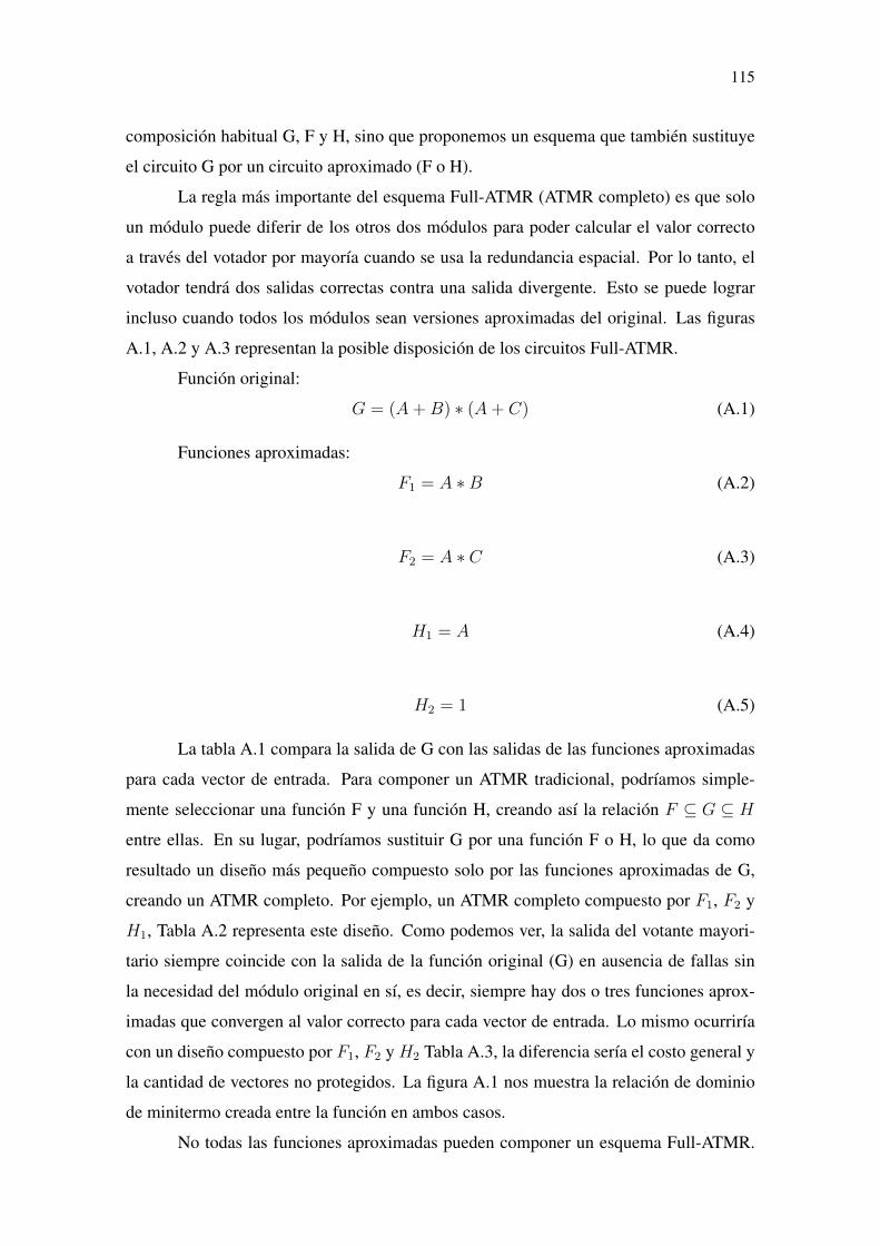
115
composición habitual G, F y H, sino que proponemos un esquema que también sustituye
el circuito G por un circuito aproximado (F o H).
La regla más importante del esquema Full-ATMR (ATMR completo) es que solo
un módulo puede diferir de los otros dos módulos para poder calcular el valor correcto
a través del votador por mayoría cuando se usa la redundancia espacial. Por lo tanto, el
votador tendrá dos salidas correctas contra una salida divergente. Esto se puede lograr
incluso cuando todos los módulos sean versiones aproximadas del original. Las figuras
A.1, A.2 y A.3 representan la posible disposición de los circuitos Full-ATMR.
Función original:
G = (A + B) ∗ (A + C) (A.1)
Funciones aproximadas:
F1 = A ∗B (A.2)
F2 = A ∗ C (A.3)
H1 = A (A.4)
H2 = 1 (A.5)
La tabla A.1 compara la salida de G con las salidas de las funciones aproximadas
para cada vector de entrada. Para componer un ATMR tradicional, podríamos simple-
mente seleccionar una función F y una función H, creando así la relación F ⊆ G ⊆ H
entre ellas. En su lugar, podríamos sustituir G por una función F o H, lo que da como
resultado un diseño más pequeño compuesto solo por las funciones aproximadas de G,
creando un ATMR completo. Por ejemplo, un ATMR completo compuesto por F1, F2 y
H1, Tabla A.2 representa este diseño. Como podemos ver, la salida del votante mayori-
tario siempre coincide con la salida de la función original (G) en ausencia de fallas sin
la necesidad del módulo original en sí, es decir, siempre hay dos o tres funciones aprox-
imadas que convergen al valor correcto para cada vector de entrada. Lo mismo ocurriría
con un diseño compuesto por F1, F2 y H2 Tabla A.3, la diferencia sería el costo general y
la cantidad de vectores no protegidos. La figura A.1 nos muestra la relación de dominio
de minitermo creada entre la función en ambos casos.
No todas las funciones aproximadas pueden componer un esquema Full-ATMR.

116
Table A.1: Truth table for candidates functions.Vectors(ABC) G F1 F2 H1 H2
MintermsMaxterms
000 0 0 0 0 1 m0001 0 0 0 0 1 m1010 0 0 0 0 1 m2011 0 0 0 0 1 m3100 0 0 0 1 1 m4101 1 0 1 1 1 m5110 1 1 0 1 1 m6111 1 1 1 1 1 m7
Table A.2: Truth table for a FATMR composed by F1,F2 and H1.Vectors(ABC) F1 F2 H1
Voteroutput
000 0 0 0 0001 0 0 0 0010 0 0 0 0011 0 0 0 0100 0 0 1 0101 0 1 1 1110 1 0 1 1111 1 1 1 1
Para que dos (o incluso tres) funciones del mismo tipo (F o H) compongan el diseño, es
necesario que ninguna de ellas diverja de G en el mismo vector de entrada. Por ejemplo,
F1 y F2 son sub-aproximados, pero difieren de G en un conjunto diferente de términos
mínimos (m5 para F1 y m6 para F2). No podemos diseñar un ATMR completo compuesto
por H1 y H2 y cualquier otra función. En este caso (Tabla A.4) ambos H1 y H2 y divergen
de G en el mismo vector de entrada (100), lo que produce un valor incorrecto en la salida
del votador en ausencia de fallas.
Suponiendo que para un diseño dado podamos encontrar dos funciones H para
componer el ATMR completo, la figura A.2 representa la relación para un ATMR com-
pleto compuesto por dos funciones H y una función F. Otra posibilidad es que todas las
funciones fueran del mismo tipo (F o H), en este caso Figure A.3 representa la relación
para un ATMR completo compuesto por tres funciones del mismo tipo, F (sub-aproximado)
y H (sobre-aproximado).

117
Table A.3: Truth table for a FATMR composed by F1,F2 and H2.Vectors(ABC) F1 F2 H1
Voteroutput
000 0 0 1 0001 0 0 1 0010 0 0 1 0011 0 0 1 0100 0 0 1 0101 0 1 1 1110 1 0 1 1111 1 1 1 1
Table A.4: Truth table for a FATMR composed by F1,H1 and H2.Vectors(ABC) F1 H1 H2
Voteroutput
000 0 0 1 0001 0 0 1 0010 0 0 1 0011 0 0 1 0100 0 1 1 0⇒1101 0 1 1 1110 1 1 1 1111 1 1 1 1
Figure A.1: Representación gráfica de la relación de funciones para un Full-ATMR com-puesto por dos funciones sub-aproximadas y una sobre-aproximada. El área gris estáprotegida, es decir, todas las funciones convergen al mismo valor.
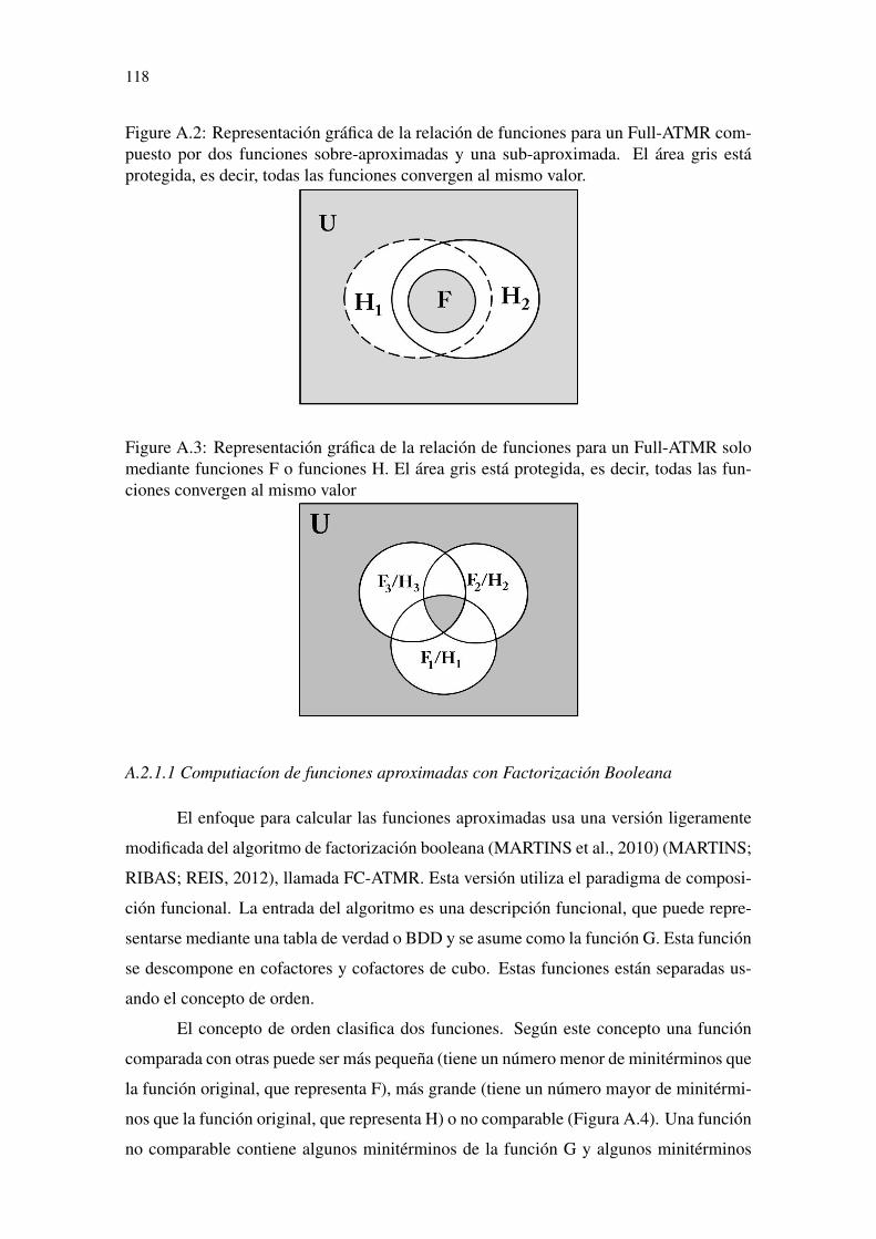
118
Figure A.2: Representación gráfica de la relación de funciones para un Full-ATMR com-puesto por dos funciones sobre-aproximadas y una sub-aproximada. El área gris estáprotegida, es decir, todas las funciones convergen al mismo valor.
Figure A.3: Representación gráfica de la relación de funciones para un Full-ATMR solomediante funciones F o funciones H. El área gris está protegida, es decir, todas las fun-ciones convergen al mismo valor
A.2.1.1 Computiacíon de funciones aproximadas con Factorización Booleana
El enfoque para calcular las funciones aproximadas usa una versión ligeramente
modificada del algoritmo de factorización booleana (MARTINS et al., 2010) (MARTINS;
RIBAS; REIS, 2012), llamada FC-ATMR. Esta versión utiliza el paradigma de composi-
ción funcional. La entrada del algoritmo es una descripción funcional, que puede repre-
sentarse mediante una tabla de verdad o BDD y se asume como la función G. Esta función
se descompone en cofactores y cofactores de cubo. Estas funciones están separadas us-
ando el concepto de orden.
El concepto de orden clasifica dos funciones. Según este concepto una función
comparada con otras puede ser más pequeña (tiene un número menor de minitérminos que
la función original, que representa F), más grande (tiene un número mayor de minitérmi-
nos que la función original, que representa H) o no comparable (Figura A.4). Una función
no comparable contiene algunos minitérminos de la función G y algunos minitérminos
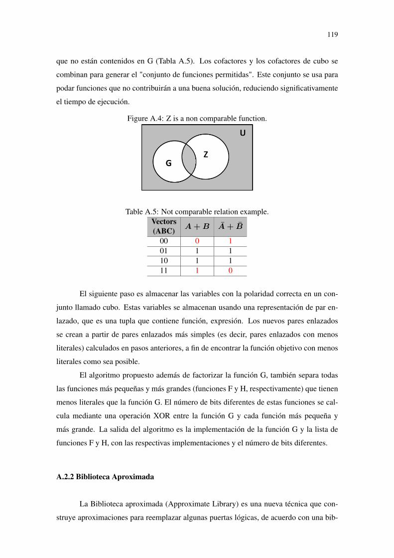
119
que no están contenidos en G (Tabla A.5). Los cofactores y los cofactores de cubo se
combinan para generar el "conjunto de funciones permitidas". Este conjunto se usa para
podar funciones que no contribuirán a una buena solución, reduciendo significativamente
el tiempo de ejecución.
Figure A.4: Z is a non comparable function.
Table A.5: Not comparable relation example.Vectors(ABC) A + B A + B
00 0 101 1 110 1 111 1 0
El siguiente paso es almacenar las variables con la polaridad correcta en un con-
junto llamado cubo. Estas variables se almacenan usando una representación de par en-
lazado, que es una tupla que contiene función, expresión. Los nuevos pares enlazados
se crean a partir de pares enlazados más simples (es decir, pares enlazados con menos
literales) calculados en pasos anteriores, a fin de encontrar la función objetivo con menos
literales como sea posible.
El algoritmo propuesto además de factorizar la función G, también separa todas
las funciones más pequeñas y más grandes (funciones F y H, respectivamente) que tienen
menos literales que la función G. El número de bits diferentes de estas funciones se cal-
cula mediante una operación XOR entre la función G y cada función más pequeña y
más grande. La salida del algoritmo es la implementación de la función G y la lista de
funciones F y H, con las respectivas implementaciones y el número de bits diferentes.
A.2.2 Biblioteca Aproximada
La Biblioteca aproximada (Approximate Library) es una nueva técnica que con-
struye aproximaciones para reemplazar algunas puertas lógicas, de acuerdo con una bib-
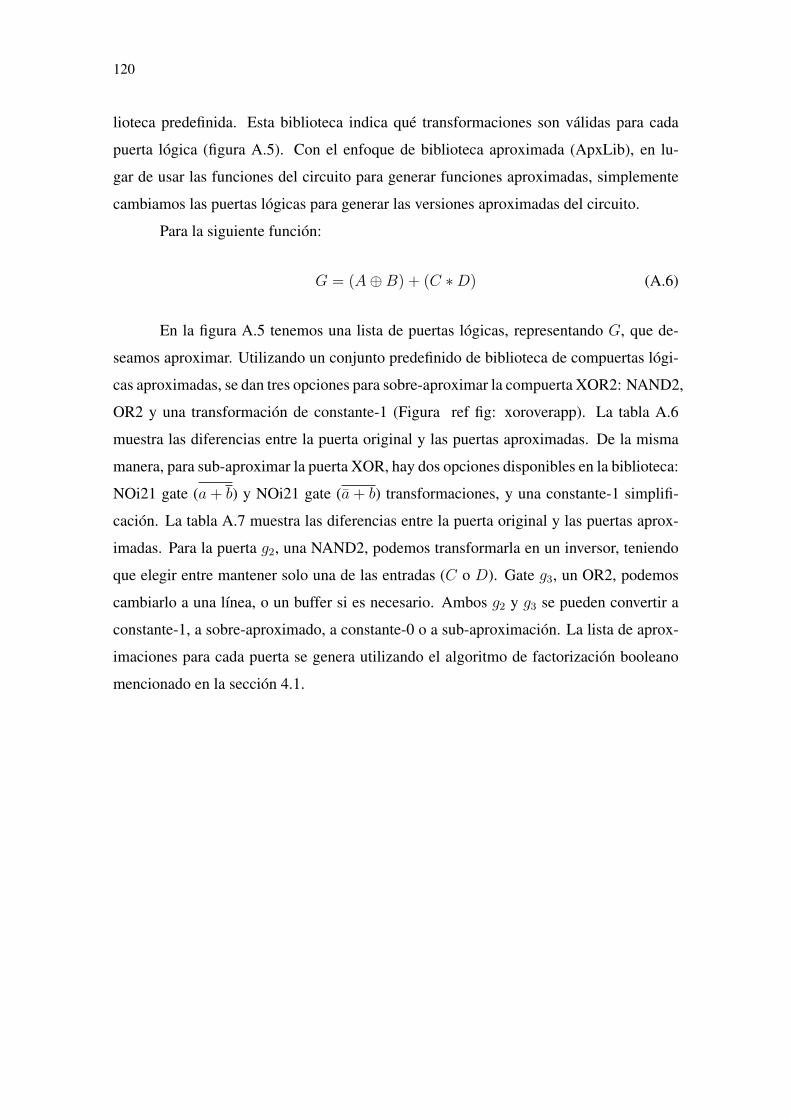
120
lioteca predefinida. Esta biblioteca indica qué transformaciones son válidas para cada
puerta lógica (figura A.5). Con el enfoque de biblioteca aproximada (ApxLib), en lu-
gar de usar las funciones del circuito para generar funciones aproximadas, simplemente
cambiamos las puertas lógicas para generar las versiones aproximadas del circuito.
Para la siguiente función:
G = (A⊕B) + (C ∗D) (A.6)
En la figura A.5 tenemos una lista de puertas lógicas, representando G, que de-
seamos aproximar. Utilizando un conjunto predefinido de biblioteca de compuertas lógi-
cas aproximadas, se dan tres opciones para sobre-aproximar la compuerta XOR2: NAND2,
OR2 y una transformación de constante-1 (Figura ref fig: xoroverapp). La tabla A.6
muestra las diferencias entre la puerta original y las puertas aproximadas. De la misma
manera, para sub-aproximar la puerta XOR, hay dos opciones disponibles en la biblioteca:
NOi21 gate (a + b) y NOi21 gate (a + b) transformaciones, y una constante-1 simplifi-
cación. La tabla A.7 muestra las diferencias entre la puerta original y las puertas aprox-
imadas. Para la puerta g2, una NAND2, podemos transformarla en un inversor, teniendo
que elegir entre mantener solo una de las entradas (C o D). Gate g3, un OR2, podemos
cambiarlo a una línea, o un buffer si es necesario. Ambos g2 y g3 se pueden convertir a
constante-1, a sobre-aproximado, a constante-0 o a sub-aproximación. La lista de aprox-
imaciones para cada puerta se genera utilizando el algoritmo de factorización booleano
mencionado en la sección 4.1.
121
Figure A.5: Biblioteca approximada: cada puerta lógica puede ser reemplazada por unapuerta aproximada de la biblioteca.
Table A.6: Posibilidades de sobre-aproximaccion para puerta XOR.
Inputs
(AB)A⊕B A ∗B A + B Const-1
00 0 1 0 1
01 1 1 1 1
10 1 1 1 1
11 0 0 1 1
Table A.7: Posibilidades de sub-aproximaccion para puerta XOR.
Inputs
(AB)A⊕B A + B A + B Const-0
00 0 0 0 0
01 1 0 1 0
10 1 1 0 0
11 0 0 0 0
Ahora veamos cómo cada una de las transformaciones XOR afecta el circuito final.
Las aproximaciones generales generarían las siguientes funciones.
122
Cambiar la puerta XOR a la puerta NAND2:
H1 = (A ∗B) + (C ∗D) (A.7)
Cambiar la puerta XOR a la puerta OR2:
H2 = (A + B) + (C ∗D) (A.8)
La figura A.6 muestra el mapa de Karnaugh para las funciones de aproximación
generadas al hacer las transformaciones basadas en el enfoque de la biblioteca aproxi-
mada. Como podemos ver, algunos de los valores han cambiado de 0 a 1, creando fun-
ciones lógicas sobre-aproximadas como se esperaba.
Figure A.6: Mapa de Karnaugh para las funciones sobre-aproximadas finales de G.
(a) G = (A⊕B) + (C ∗D)
(b) H1 = (A ∗B) + (C ∗D) (c) H2 = (A+B) + (C ∗D)
Las sub-aproximaciones generarían las siguientes funciones.
Cambiar la puerta XOR a la puerta NOi21 tipo 1:
F1 = (A + B) + (C ∗D) (A.9)
Cambiar la puerta XOR a la puerta NOi21 tipo 2:
F2 = (A + B) + (C ∗D) (A.10)
La figura A.7 muestra el mapa de Karnaugh para las funciones sub-aproximadas
123
generadas al hacer las transformaciones basadas en el enfoque de la biblioteca aproxi-
mada. Como podemos ver, algunos de los valores cambiaron de 1 a 0, creando una lógica
de funciones sub-aproximadas como se esperaba.
Figure A.7: Mapa de Karnaugh para las funciones sub-aproximadas finales de G.
(a) G = (A⊕B) + (C ∗D)
(b) F1 = (A+B) + (C ∗D)) (c) F2 = (A+B) + (C ∗D))
A.2.3 ApxLib+MOOGA
Muchos problemas de optimización del mundo real son extremadamente difí-
ciles y complejos en términos de número de variables, naturaleza de la función objetivo,
número de óptimos locales, espacios de búsqueda continuos o discretos, tiempo y recursos
de cálculo requeridos, etc. (AMOUZGAR, 2012). El enfoque de Biblioteca Aproximada
comparte la misma complejidad que algunos problemas multiobjetivo en diferentes do-
minios como los servicios, el comercio y la ingenieria. Cada modificación en el circuito
genera una gran cantidad de nuevas modificaciones posibles, aumentando la lista de solu-
ciones muy rápidamente.
La idea de utilizar un Algoritmo Genético de Optimización Multiobjetivo (MOOGA),
(AMOUZGAR, 2012) (SERRANO-CASES et al., 2016), con el enfoque ApxLib, (AL-
BANDES et al., 2018b), tiene como objetivo hacer una búsqueda ciega dentro de todo el
espacio de soluciones posibles, para posteriormente con la clasificación de Optimización
multiobjetivo, seleccionar las mejores configuraciones que reduzcan el área y maximicen
la cobertura a fallos.
124
La figura A.8 muestra el flujo del algoritmo ApxLib+MOOGA. La figura aclara la
integración del algoritmo de clasificación MOO y GA con el enfoque ApxLib. También
muestra las fases del algoritmo. En primer lugar, se realiza un análisis del circuito para
evaluar las características del circuito original. El algoritmo evalúa las paridades y las
posibles aproximaciones de las puertas para definir el genotipo del circuito. Después de
eso, se realiza una fase de inicialización donde se aplican los operadores de mutación
en el genotipo original, como resultado se obtiene la primera generación de individuos.
Luego, el algoritmo inicia una iteración para generar la siguiente población.
La etapa de evaluación está a cargo del segundo análisis del circuito, que verifica
si los individuos ATMR generados son correctos, luego evalúa el tamaño y los valores de
enmascaramiento de fallos de esos circuitos. Después de eso, los recálculos dinámicos
de los genes reevaluan algunos parámetros de los circuitos aproximados que se utilizarán
en las siguientes iteraciones del algoritmo. El siguiente paso del algoritmo MOOGA es
la clasificación de optimización multiobjetivo (clasificación MOO), que está a cargo del
mecanismo de selección, es decir, elegir los mejores circuitos para la próxima iteración.
Finalmente, el cruce y la mutación se realiza con los mejores circuitos de la población. En
resumen, el operador de selección selecciona y mantiene las buenas soluciones; mientras
que el crossover recombina las soluciones para crear una buena descendencia y el oper-
ador de mutaciones altera aleatoriamente genes en un individuo para poder encontrar un
mejor genotipo. Estas etapas se repiten hasta que lleguemos a cien generaciones.

125
Figure A.8: MOOGA+ApxLib Algorithm flow
A.2.3.1 Genotipo, cromosomas y definición de genes
Como se mencionó, en el algoritmo genético, a diferencia de otros métodos clási-
cos, se crea y selecciona una población aleatoria. En nuestro caso, la población está
compuesta por esquemas ATMR que serán los individuos. Cada individuo se representa
como un conjunto de parámetros que se conocen como cromosomas. La unión de los
cromosomas de un individuo se llama genotipo.
Para definir el genotipo de un individuo primero se realiza un análisis para evaluar
las características del circuito. En este análisis, la paridad, las sobre-aproximaciones
y las sub-aproximaciones se evalúan para crear el perfil genético (el genotipo). Cada
cromosoma en el genotipo se basa en una puerta, y los genes en ese cromosoma son las

126
características de esa puerta. Para un cromosoma de la puerta Gx, los genes son:
• Approximation : este gen define qué transformación está usando la puerta. El
valor 0 significa la puerta original. Los valores superiores a 0 definen el código de
la aproximación.
• Used : este gen define si la puerta está siendo utilizada por el circuito. Algunas
aproximaciones pueden desconectar una puerta del circuito.
• Parity : informa cuál es la paridad de la puerta, positiva (1), negativa (-1) o sin
paridad (0).
• Over - apx : el número de sobre-aproximaciones posibles para la puerta.
• Under - apx : el número de sub-aproximaciones posibles para la puerta.
Tomemos el circuito G (Figura A.9) como ejemplo. El análisis del circuito nos
devuelve los valores de paridad y aproximaciones en la tabla A.8. Los cromosomas resul-
tantes se muestran en la figura A.10.
Figure A.9: Original circuit G
Figure A.10: Original circuit G chromosomes.
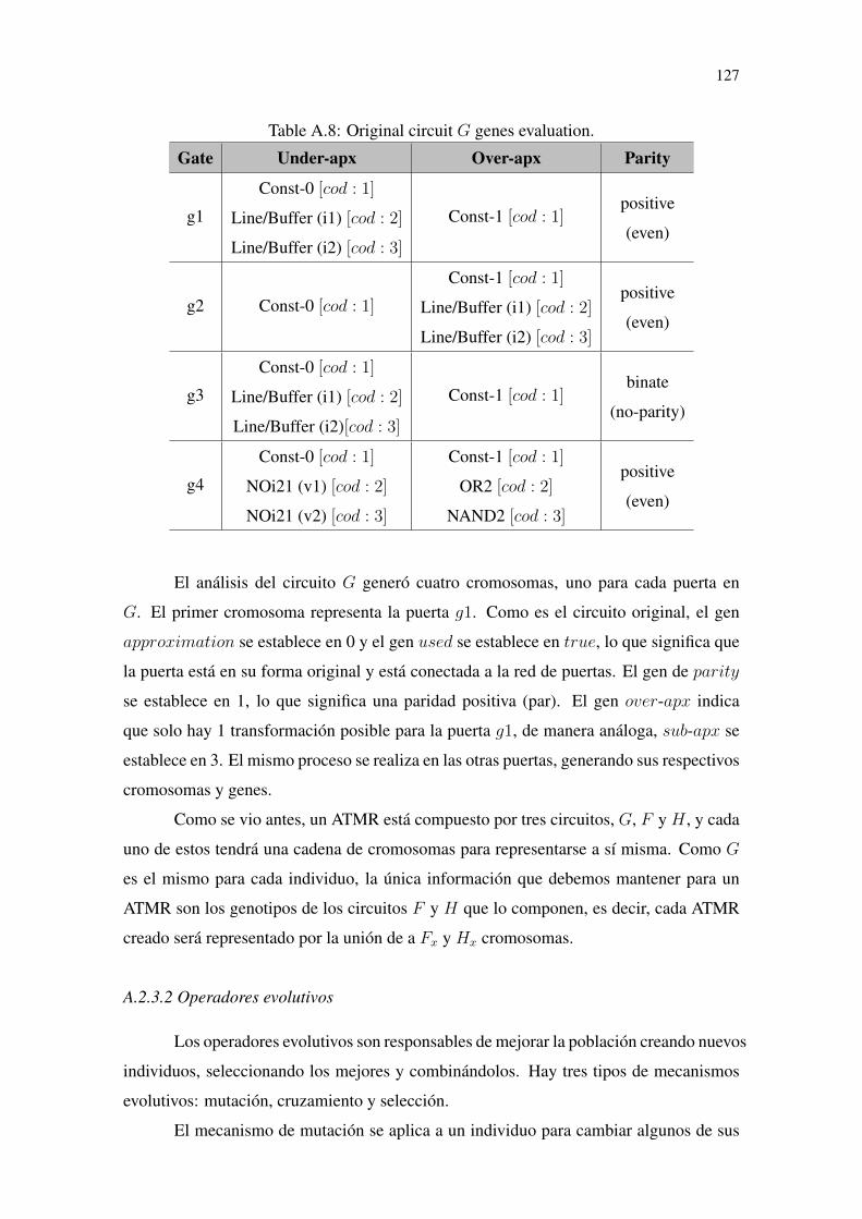
127
Table A.8: Original circuit G genes evaluation.
Gate Under-apx Over-apx Parity
g1
Const-0 [cod : 1]
Line/Buffer (i1) [cod : 2]
Line/Buffer (i2) [cod : 3]
Const-1 [cod : 1]positive
(even)
g2 Const-0 [cod : 1]
Const-1 [cod : 1]
Line/Buffer (i1) [cod : 2]
Line/Buffer (i2) [cod : 3]
positive
(even)
g3
Const-0 [cod : 1]
Line/Buffer (i1) [cod : 2]
Line/Buffer (i2)[cod : 3]
Const-1 [cod : 1]binate
(no-parity)
g4
Const-0 [cod : 1]
NOi21 (v1) [cod : 2]
NOi21 (v2) [cod : 3]
Const-1 [cod : 1]
OR2 [cod : 2]
NAND2 [cod : 3]
positive
(even)
El análisis del circuito G generó cuatro cromosomas, uno para cada puerta en
G. El primer cromosoma representa la puerta g1. Como es el circuito original, el gen
approximation se establece en 0 y el gen used se establece en true, lo que significa que
la puerta está en su forma original y está conectada a la red de puertas. El gen de parity
se establece en 1, lo que significa una paridad positiva (par). El gen over-apx indica
que solo hay 1 transformación posible para la puerta g1, de manera análoga, sub-apx se
establece en 3. El mismo proceso se realiza en las otras puertas, generando sus respectivos
cromosomas y genes.
Como se vio antes, un ATMR está compuesto por tres circuitos, G, F y H , y cada
uno de estos tendrá una cadena de cromosomas para representarse a sí misma. Como G
es el mismo para cada individuo, la única información que debemos mantener para un
ATMR son los genotipos de los circuitos F y H que lo componen, es decir, cada ATMR
creado será representado por la unión de a Fx y Hx cromosomas.
A.2.3.2 Operadores evolutivos
Los operadores evolutivos son responsables de mejorar la población creando nuevos
individuos, seleccionando los mejores y combinándolos. Hay tres tipos de mecanismos
evolutivos: mutación, cruzamiento y selección.
El mecanismo de mutación se aplica a un individuo para cambiar algunos de sus

128
genes. En nuestro proceso, el único gen mutado es el aproximation. Después de que
la mutación se procesa el genotipo, se crea una representación de circuito y luego se
reevalúan los genes parity y used.
Hay varios operadores de cruce diferentes en la literatura, pero el concepto prin-
cipal es seleccionar dos individuos (genotipos) de la población e intercambiar una por-
ción de estos genotipos entre ellos para crear un nuevo individuo. Este proceso también
se conoce como apareamiento, y el nuevo individuo a menudo se llama descendencia
(offspring). En nuestro enfoque utilizamos el operador de cruce de punto único. En
este tipo de cruce, se define un punto px en el genotipo, donde p0 es el primer cromosoma
y pn es el último cromosoma. La descendencia estará compuesta por los cromosomas
entre p0 a px de uno de los padres, y los cromosomas px+1 a pn del otro padre (Figura
A.11). En nuestro enfoque, px es siempre el punto medio del genotipo, y el cruce genera
dos descendientes. Al hacer esto, estamos creando un nuevo ATMR intercambiando los
módulos F y H entre entonces.
Figure A.11: Single point crossover.
La selección es responsable de clasificar a los individuos en la población. Las
soluciones que se clasifican mejor tienen una mejor oportunidad de cruzarse y crear de-
scendencia, mientras que los individuos peor calificadas tienen menos posibilidades de
aparearse con otros. El principal objetivo del operador de selección es mantener y mejo-
rar a los individuos en cada nueva generación, manteniendo constante el tamaño de la
generación. Nuestro enfoque utiliza un NSGA-II (algoritmo genético de ordenación no
dominado II) para establecer una relación de orden entre los individuos de una población
basada principalmente en el concepto de no dominancia o frentes de Pareto (DEB et al.,
2002). Se dice que una solución Xi domina otros Xj si el primero es mejor o igual que el
segundo en cada objetivo y, al menos, estrictamente mejor en uno de ellos (es decir, los
frentes de Pareto están definidos por aquellos puntos en los que las mejoras en un objetivo
no son posibles sin degradar el resto de los objetivos).

129
A.2.4 ApxLib+Heuristic
Este enfoque se basa en el uso de la técnica de biblioteca aproximada con heurís-
tica para construir aproximaciones de una manera más rápida y determinista. Las medidas
de testabilidad y observabilidad guían la creación de una versión aproximada del circuito.
Usando esta técnica, las soluciones ATMR pueden tomar unos minutos en lugar de horas
y los resultados muestran que, en algunos casos, se puede lograr una buena compensación
entre la sobrecarga del área y el enmascaramiento de fallos.
El enfoque de biblioteca aproximado (ApxLib) genera circuitos aproximados me-
diante la transformación de las puertas lógicas basadas en un preajuste de posibles trans-
formaciones. Después de definir que una puerta determinada es la mejor candidata para
la aproximación, la heurística selecciona la transformación de puerta más adecuada. El
algoritmo sigue los siguietes pasos:
1. Evaluación de la influencia de cada puerta con respecto a los resultados
2. Análisis de las posibles transformaciones para las puertas que tienen poca influencia
en el circuito
3. Selección de la mejor transformación de puerta
4. Aproximación de la puerta elegida
5. Vuelve al paso uno hasta que no haya más aproximaciones posibles
Podemos simplificar el proceso heurístico dividiéndolo en tan solo tres pasos: 1.
evaluación de las puertas candidatas; 2. evaluación de aproximaciones de candidatos; 3.
selección heurística de la mejor aproximación basada en los pasos 1 y 2; Y luego el pro-
ceso se repite hasta que sea necesario. Una vez hecho este proceso, el algoritmo generará
docenas de circuitos aproximados, que luego se optimizarán lógicamente y se sintetizarán
utilizando una biblioteca de células. Después de sintetizar los circuitos, la inyección de
fallos se realiza para evaluar la tasa de errores de los circuitos ATMR creados. (Figura
A.12)
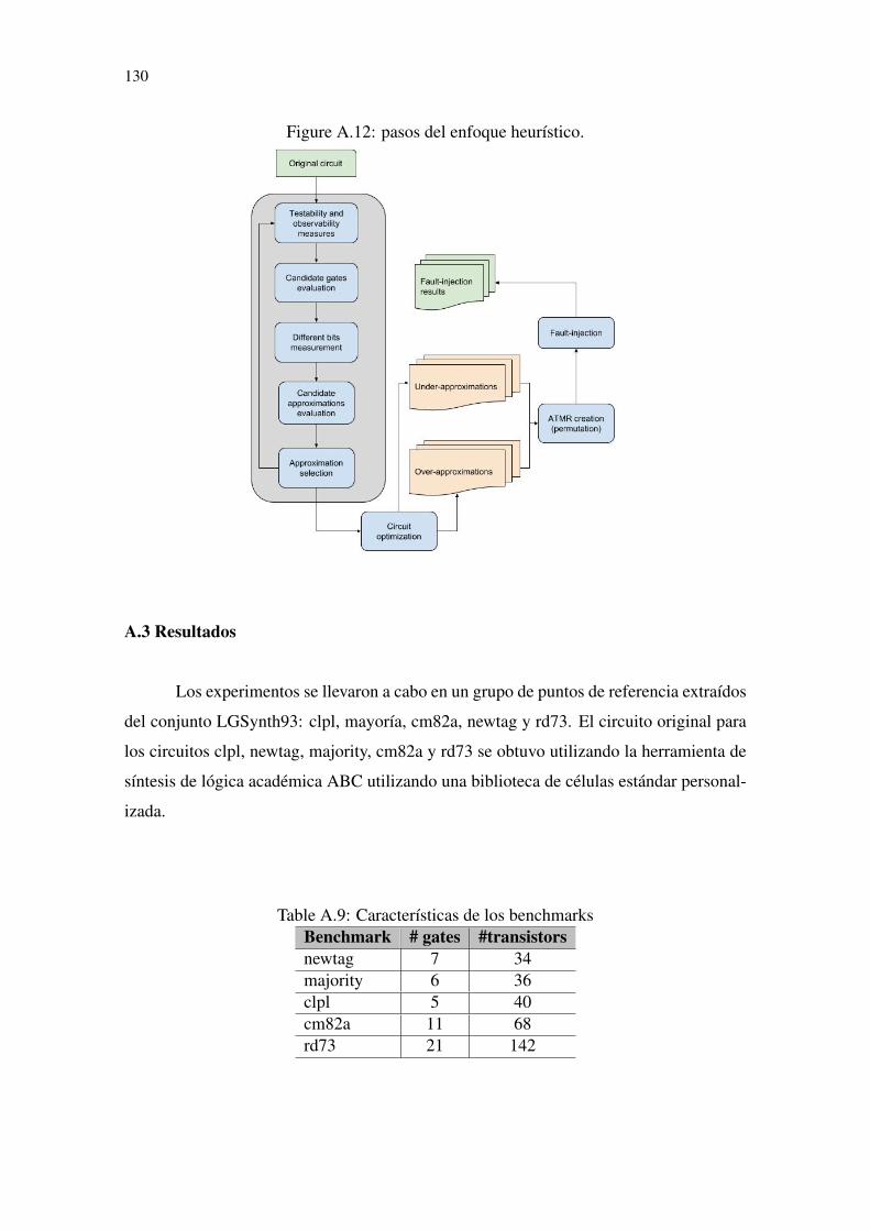
130
Figure A.12: pasos del enfoque heurístico.
A.3 Resultados
Los experimentos se llevaron a cabo en un grupo de puntos de referencia extraídos
del conjunto LGSynth93: clpl, mayoría, cm82a, newtag y rd73. El circuito original para
los circuitos clpl, newtag, majority, cm82a y rd73 se obtuvo utilizando la herramienta de
síntesis de lógica académica ABC utilizando una biblioteca de células estándar personal-
izada.
Table A.9: Características de los benchmarksBenchmark # gates #transistorsnewtag 7 34majority 6 36clpl 5 40cm82a 11 68rd73 21 142
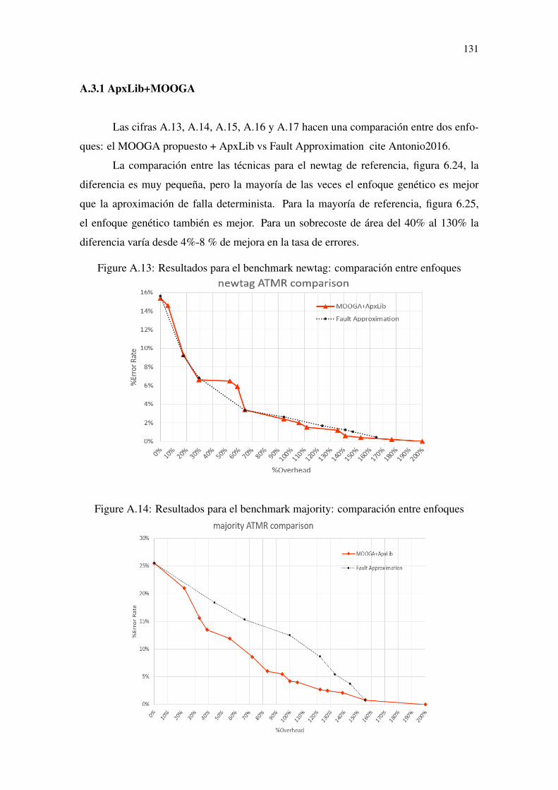
131
A.3.1 ApxLib+MOOGA
Las cifras A.13, A.14, A.15, A.16 y A.17 hacen una comparación entre dos enfo-
ques: el MOOGA propuesto + ApxLib vs Fault Approximation cite Antonio2016.
La comparación entre las técnicas para el newtag de referencia, figura 6.24, la
diferencia es muy pequeña, pero la mayoría de las veces el enfoque genético es mejor
que la aproximación de falla determinista. Para la mayoría de referencia, figura 6.25,
el enfoque genético también es mejor. Para un sobrecoste de área del 40% al 130% la
diferencia varía desde 4%-8 % de mejora en la tasa de errores.
Figure A.13: Resultados para el benchmark newtag: comparación entre enfoques
Figure A.14: Resultados para el benchmark majority: comparación entre enfoques
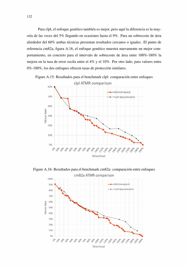
132
Para clpl, el enfoque genético también es mejor, pero aquí la diferencia es la may-
oría de las veces del 5% llegando en ocasiones hasta el 9%. Para un sobrecoste de área
alrededor del 60% ambas técnicas presentan resultados cercanos o iguales. El punto de
referencia cm82a, figura A.16, el enfoque genético muestra nuevamente un mejor com-
portamiento, en concreto para el intervalo de sobrecoste de área entre 100%-180% la
mejora en la tasa de error oscila entre el 4% y el 10%. Por otro lado, para valores entre
0%-100%, los dos enfoques ofrecen tasas de protección similares.
Figure A.15: Resultados para el benchmark clpl: comparación entre enfoques
Figure A.16: Resultados para el benchmark cm82a: comparación entre enfoques
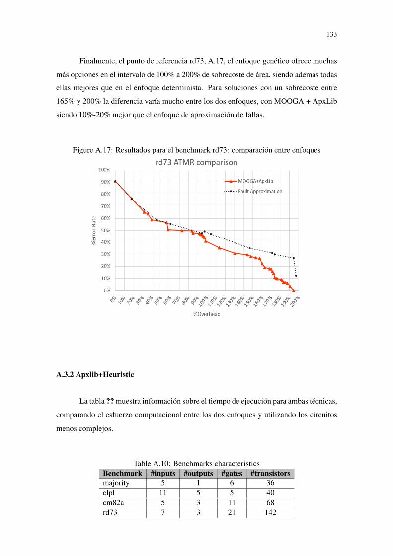
133
Finalmente, el punto de referencia rd73, A.17, el enfoque genético ofrece muchas
más opciones en el intervalo de 100% a 200% de sobrecoste de área, siendo además todas
ellas mejores que en el enfoque determinista. Para soluciones con un sobrecoste entre
165% y 200% la diferencia varía mucho entre los dos enfoques, con MOOGA + ApxLib
siendo 10%-20% mejor que el enfoque de aproximación de fallas.
Figure A.17: Resultados para el benchmark rd73: comparación entre enfoques
A.3.2 Apxlib+Heuristic
La tabla ?? muestra información sobre el tiempo de ejecución para ambas técnicas,
comparando el esfuerzo computacional entre los dos enfoques y utilizando los circuitos
menos complejos.
Table A.10: Benchmarks characteristicsBenchmark #inputs #outputs #gates #transistorsmajority 5 1 6 36clpl 11 5 5 40cm82a 5 3 11 68rd73 7 3 21 142

134
Table A.11: Execution time: MOOGA vs Heuristic
BenchmarksExecution Time
ApxLib+MOOGA ApxLib+Heuristic
majority ∼1h30m ∼1min
clpl ∼1h30m ∼1min
cm82a ∼1h30m ∼1min
Rd73 ∼3h30m ∼1min
Cada esquema de ATMR resultante ha sido evaluado con respecto a la tasa de
enmascaramiento de error usando la simulación para la inyección de fallos. Debido al
pequeño tamaño de los puntos de referencia considerados, se ha realizado un análisis
exhaustivo, inyectando fallas en la salida de cada compuerta en el circuito ATMR (ex-
cluyendo al votador) para cada vector de entrada posible. Igualmente, para la evaluación
del enfoque heurístico se realizó un análisis exhaustivo de las medidas del cálculo de los
diferentes bits.
Los resultados para la inyección de fallas se hicieron usando un simulador hecho a
medida utilizando el lenguaje python. El sobrecoste en área de los circuitos se calculó en
base a la cantidad de transistores del circuito ATMR. Todo el proceso ApxLib + MOOGA
requiere un esfuerzo computacional de varias horas para generar los resultados finales. Sin
embargo, el tiempo de computación de la aproximación determinista, ApxLib + Heuristic,
está en el orden del minuto.
Las cifras A.18, A.19, A.20 y A.21 muestran toda la población generada por el
enfoque ApxLib + MOOGA (marcadores azules). Los mejores resultados generados por
ApxLib + MOOGA están representados por círculos negros con la línea negra que los
conecta (frente de Pareto). Además, los marcadores rojos representan los mejores resul-
tados generados por ApxLib + enfoque heurístico.
La figura A.18, muestra los resultados del benchmark mayoritario. Como puede
apreciarse, para un sobrecoste de área entre el 200% y el 30%, el enfoque heurístico
mantiene valores de tasa de error cercanos a los obtenidos por el enfoque del algoritmo
genético. La heurística también se mantiene a una buena distancia de los peores circuitos
posibles de la población.
Podemos ver en A.19, resultados para el benchmark clp, que para valores de sobre-
coste más altos, entre 160%-200%, la tasa de error es casi la misma para ambas técnicas (
el enfoque genético ofrece un pequeño márgen de mejora). Para sobrecostes inferiores al
120%, el enfoque heurístico comienza a empeorar significativamente en comparación con
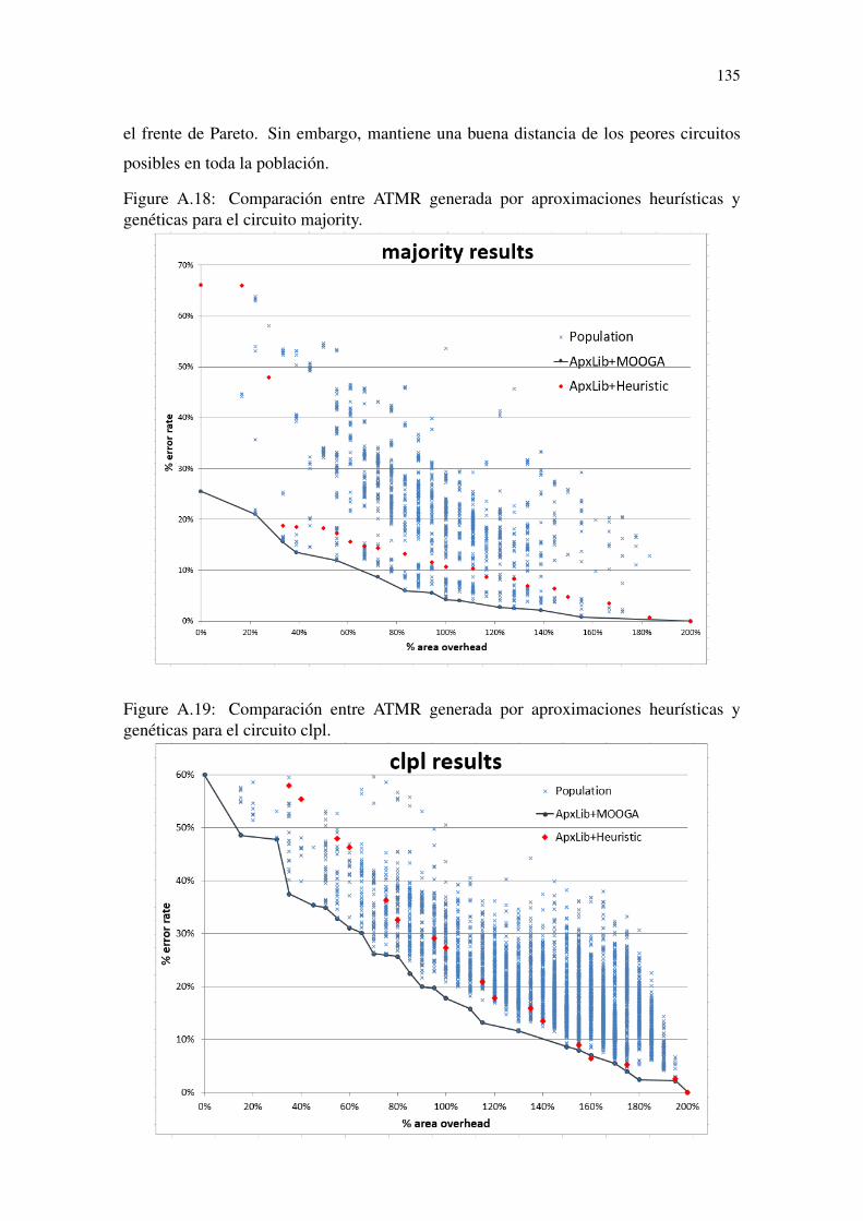
135
el frente de Pareto. Sin embargo, mantiene una buena distancia de los peores circuitos
posibles en toda la población.
Figure A.18: Comparación entre ATMR generada por aproximaciones heurísticas ygenéticas para el circuito majority.
Figure A.19: Comparación entre ATMR generada por aproximaciones heurísticas ygenéticas para el circuito clpl.
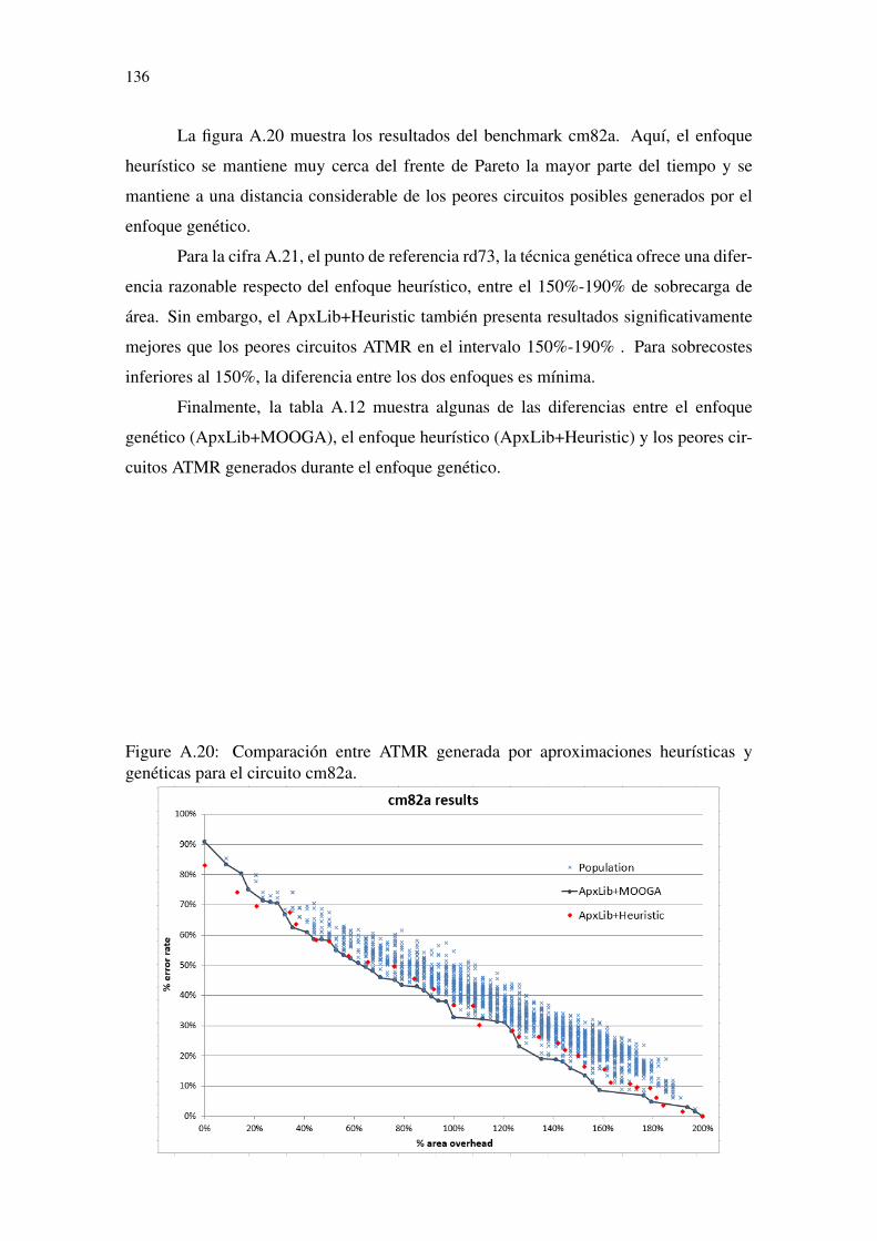
136
La figura A.20 muestra los resultados del benchmark cm82a. Aquí, el enfoque
heurístico se mantiene muy cerca del frente de Pareto la mayor parte del tiempo y se
mantiene a una distancia considerable de los peores circuitos posibles generados por el
enfoque genético.
Para la cifra A.21, el punto de referencia rd73, la técnica genética ofrece una difer-
encia razonable respecto del enfoque heurístico, entre el 150%-190% de sobrecarga de
área. Sin embargo, el ApxLib+Heuristic también presenta resultados significativamente
mejores que los peores circuitos ATMR en el intervalo 150%-190% . Para sobrecostes
inferiores al 150%, la diferencia entre los dos enfoques es mínima.
Finalmente, la tabla A.12 muestra algunas de las diferencias entre el enfoque
genético (ApxLib+MOOGA), el enfoque heurístico (ApxLib+Heuristic) y los peores cir-
cuitos ATMR generados durante el enfoque genético.
Figure A.20: Comparación entre ATMR generada por aproximaciones heurísticas ygenéticas para el circuito cm82a.

137
Figure A.21: Comparación entre ATMR generada por aproximaciones heurísticas ygenéticas para el circuito rd73.
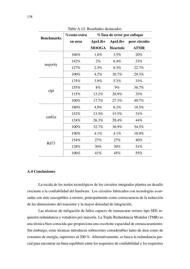
138
Table A.12: Resultados destacados.
Benchmarks%costo extra
en area
%Tasa de error por enfoque
ApxLib+
MOOGA
ApxLib+
Heuristic
peor circuito
ATMR
majority
166% 1.8% 3.5% 20%
142% 2% 6.4% 33%
127% 2.5% 8.3% 22.7%
100% 4.2% 10.7% 29.3%
clpl
175% 3.9% 5.3% 33%
155% 8% 9% 36.7%
115% 13.2% 20.9% 35%
100% 17.7% 27.3% 49.7%
cm82a
180% 4.8% 6.2% 18.5%
152% 13.5% 15.5% 31%
124% 26.3% 28.4% 44%
100% 32.7% 36.9% 54.5%
Rd73
190% 4.1% 4.1% 18.9%
154% 27% 27% 40%
128% 30% 30% 51%
100% 41% 45% 55%
A.4 Conclusiones
La escala de los nodos tecnológicos de los circuitos integrados plantea un desafío
creciente a la confiabilidad del hardware. Los circuitos fabricados con tecnologías avan-
zadas son más susceptibles a errores, principalmente como consecuencia de la reducción
de las dimensiones del transistor y la mayor densidad de integración.
Las técnicas de mitigación de fallos capaces de enmascarar errores tipo SEE re-
quieren redundancia y votadores por mayoría. La Triple Redundancia Modular (TMR) es
una técnica bien conocida que proporciona una excelente capacidad de enmascaramiento.
Sin embargo, estas técnicas introducen sobrecostes considerables tanto de área como de
consumo de energía, superiores al 200 %. Alternativamente, se busca la redundancia par-
cial para encontrar un buen equilibrio entre los requisitos de confiabilidad y los requisitos
139
de área, potencia y rendimiento.
Dentro de este contexto, recientemente han surgido circuitos aproximados como
un enfoque alternativo para construir soluciones parciales de TMR. Un circuito lógico
aproximado es un circuito que realiza una función lógica diferente pero estrechamente
relacionada con el circuito original. Como no se requiere que el circuito original coincida
exactamente, el circuito aproximado puede ser más pequeño, pero aún se puede usar como
réplicas en el TMR para ser evaluado por el votador mayoritario y consecuentemente
enmascarar fallos. Llamamos a esta aproximación aproximate-TMR (ATMR).
Este trabajo propuso tres enfoques novedosos para diseñar circuitos ATMR. El
primero es el concepto de Full-ATMR (FATMR), un diseño donde todos los módulos
de la TMR son aproximados. Full-ATMR permite una mayor reducción de los costos
indirectos y aún puede mantener una buena relación de protección. Fue posible mantener
la relación de unión p-n protegida por encima del 97% con solo un 125% de sobrecarga de
área. Para la versión ATMR de un sumador de ripple-carry de 4 bits, se proponen varias
implementaciones, que van desde 93%-136% a 96%-168% de uniones protegidas y una
sobrecarga de área, respectivamente.
El segundo enfoque fue una combinación de la Biblioteca Aproximada con el Al-
goritmo Genético de Optimización Multi-Objetivo (ApxLib+MOOGA). El enfoque se
comparó con una técnica de estado de la arte (fault approximation). El enfoque mostró un
buen equilibrio entre los requisitos de confiabilidad y el área, en general ApxLib+MOOGA
presentó mejores resultados que el método de fault approximation. Sin embargo, ApxLib+MOOGA
consumía mucho tiempo, incluso para circuitos pequeños.
El tercer y último enfoque es una combinación de la Biblioteca Aproximada con
Heurística (ApxLib+Heurístic). Este nuevo enfoque se comparó con ApxLib + MOOGA
con respecto a los circuitos creados y el tiempo de ejecución para hacerlo. El enfoque
heurístico (ApxLib+Heuristic) muestra un buen equilibrio entre los requisitos de con-
fiabilidad y el área, mientras que mantiene un bajo esfuerzo computacional cuando se
compara con la técnica genética (ApxLib + MOOGA), tomando alrededor de un minuto
en lugar de horas para generar los resultados. También podríamos ver que incluso cuando
está lejos del frente de Pareto, el enfoque ApxLib+Heuristic todavía tiene una buena ven-
taja sobre las peores soluciones posibles para todos los puntos de referencia probados. Es
probable que estos resultados prometedores puedan mejorarse haciendo algunos cambios
en la heurística del algoritmo y luego aplicar la técnica a circuitos más grandes. También
sería interesante adaptar el enfoque para usar en FPGA.
140
Esta investigación generó cuatro publicaciones (ALBANDES et al., 2015b), (AL-
BANDES et al., 2015a), (ALBANDES et al., 2018b) y (ALBANDES et al., 2018a).