user manual mab -51.doc
TRANSCRIPT

8051 Microcontroller Kit (MAB-51)
User manual
Advance TechnologySCO-160, 1st Floor, Sec-24D
Chandigarh – 160022Tel. No.: 0172 – 5086213
1
FOREWORD
With changing times micro-controller has evolved and today is part of almost every application viz. consumer electronics, communication systems automotive medical etc. With various controller architectures and easy to use compilers it has become easy to use a controller in wide range of applications with ease. There are many micro controllers available in market 89C51(ATMEL, PHILPS) PIC(MICROCHIP) etc.
With change in technology trends and introduction of latest protocols (CAN, MODBUS, I2C, SPI, USB) it is important to learn basics of micro controller with interfacing devices like SRAM, E2PROM, Stepper Motor, DC Motor, RTC, ADC, DAC, Relays, Displays. Keeping trends in mind Advance Technology has designed “Universal Board”.
The feature that separates this board from others is the configuration of these different devices in desired fashion. User is free to assign any controller Port to the device with provided connectors.
Since the Time to Market is crucial UNIVERSAL BOARD can reduce the development time since testing of basic devices can be done and by the time PCBs are manufactured designer is ready with the tested code.
2

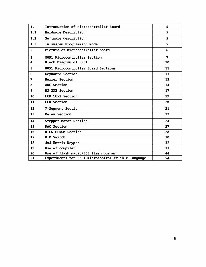
INDEXSr.No. TOPIC Page No.
1. Introduction of Microcontroller Board 5
1.1 Hardware Description 5
1.2 Software description 5
1.3 In system Programming Mode 5
2 Picture of Microcontroller board 6
3 8051 Microcontroller Section 7
4 Block Diagram of 8051 10
5 8051 Microcontroller Board Sections 11
6 Keyboard Section 13
7 Buzzer Section 13
8 ADC Section 14
9 RS 232 Section 17
10 LCD 16x2 Section 19
11 LED Section 20
12 7-Segment Section 21
13 Relay Section 22
14 Stepper Motor Section 24
15 DAC Section 27
16 RTC& EPROM Section 28
17 DIP Switch 30
18 4x4 Matrix Keypad 32
19 Use of compiler 33
20 Use of flash magic/ECE flash burner 4421 Experiments for 8051 microcontroller in c language 54
3

I/O LINES TABLE FOR 8051
Sr. No. Section I/O Lines Required
1 LED 823
7-SEGMENT you can choose any one LCD16X2 to see output
1210
4 KEYBOARD 456
4X4 KEY MATRIX BOARD you can choose any one DIP SWITCH to give Input
88
7 DAC 88 I2C 29 ADC 1610 RELAY 2
Total Pin of Microcontroller = 40Total I/O Lines Available = 32Reserved for VCC & GND = 2Reserved for Crystal Input & Output =2 Reserved for Programming & memory Interface = 4
4
INTRODUCTION
8051 MICROCONTROLLER BOARD
Hardware description
The evaluation board consists of two major parts and provides a function to convert theparallel data bus to RS232 serial port and vice versa. Also, it provides an in-systemprogramming function.
The functions of the three two parts are described as follows:• Philips P89v51RD2/P89c51RD2 is an 8051 microcontroller. The microcontroller connection to the RS232 is through the serial data bus and control signals - address, write, read, reset, and chip select signals.
• Philips RS-232 drivers/receivers are the transceivers. The first one allows themicrocontroller to be in-system programmed through a PC’s serial port such asCOM1. The RS-232 mainlyconsists of two sections: drivers (transmitters) and receivers. The drivers convert the CMOS-logic output levels to RS-232 signals, whereas the receivers convert theRS-232 signals to CMOS-logic output levels.
Software descriptionThe programming of the demo board can be done by writing firmware code requires thefollowing software.• Raisonance is one of the embedded system vendors that provide the developmenttools for the 8051 microcontroller. The software compiles the firmware code and generates an ’Intel Hex’ file. Flash Magic is a free Windows application software that allows easy programming of Philips Flash Microcontrollers. The software loads the ’Intel Hex’ file to the microcontroller by using its in-system programming mode communicating through serial port.
In-system programming mode Philips P89C51RD2/P89V51RD2 microcontroller has an on-chip Flash program memory with ISP (In-System Programming), which allows the microcontroller to be programmed without removing the microcontroller from the board and also the microcontroller, which previously programmed can be reprogrammed without removal from the board.The microcontroller must be powered up in a special ’ISP mode’ to perform the ISPoperation. The ISP mode allows the microcontroller to communicate with a host device such as PC through a serial port. The host sends commands and data to the microcontroller. The commands can be erase, read, and write. After the completion of the ISP operation, the microcontroller is reconfigured and has to be reset or power cycled so the microcontroller will operate normally. The ISP programming for the device can be
5

done using a Windows application software,which uses an Intel Hex file as input to program it.
ConclusionThe use of the evaluation kit allows the user to understand how the different external world devices are interfacing with a microcontroller such as 8051. The board shows the different peripheral devices. Which are describe below.
PICTURE OF 8051 MICROCONTROLLER BOARD
6

8051 microcontroller (P89C51RD2/P89V51RD2) section
The P89C51RB2/RC2/RD2 device contains a non-volatile 16kB/32kB/64kB Flash program memory that is both parallel programmable and serial In-System and In-Application Programmable. In-System Programming (ISP) allows the user to download new code while the microcontroller sits in the application.In-Application Programming (IAP) means that the microcontroller fetches new program code and reprograms itself while in the system. This allows for remote programming over a modem link. A default serial loader (boot loader) program in ROM allows serialIn-System programming of the Flash memory via the UART without the need for a loader in the Flash code. For In-Application Programming, the user program erases and reprograms the Flash memory by use of standard routines contained in ROM.This device executes one machine cycle in 6 clock cycles, hence providing twice the speed of a conventional 80C51. An OTP configuration bit lets the user select conventional 12 clock timing if desired. This device is a Single-Chip 8-Bit Microcontroller manufactured in advanced CMOS process and is a derivative of the 80C51 microcontroller family. The instruction set is 100% compatible with the 80C51 instruction set. The device also has four 8-bit I/O ports, three 16-bit timer/event counters, a multi-source, four-priority-level, nested interrupt structure, an enhanced UART and on-chip oscillator and timing circuits. The added features of the P89C51RB2/RC2/RD2 makes it a powerful microcontroller for applications that require pulse width modulation, high-speed I/O and up/down counting capabilities such
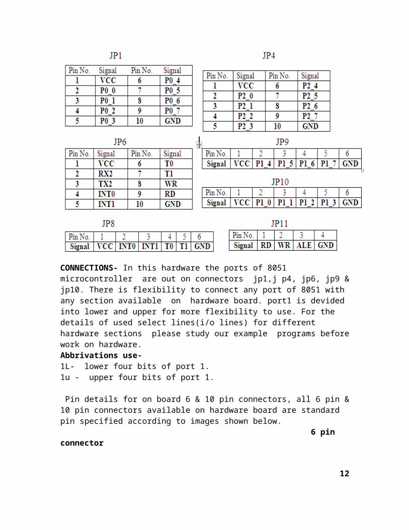
JP1 PORT P0 JP4 PORT
P2
P89C51RD2/P89V51RD22)()
JP6 PORT P3
JP9 PORT 1(upper)
Jp10 PORT 1(lower)
8051 reset
7
CONNECTIONS- In this hardware the ports of 8051 microcontroller are out on connectors jp1,j p4, jp6, jp9 & jp10. There is flexibility to connect any port of 8051 with any section available on hardware board. port1 is devided into lower and upper for more flexibility to use. For the details of used select lines(i/o lines) for different hardware sections please study our example programs before work on hardware. Abbrivations use-1L- lower four bits of port 1.1u - upper four bits of port 1.
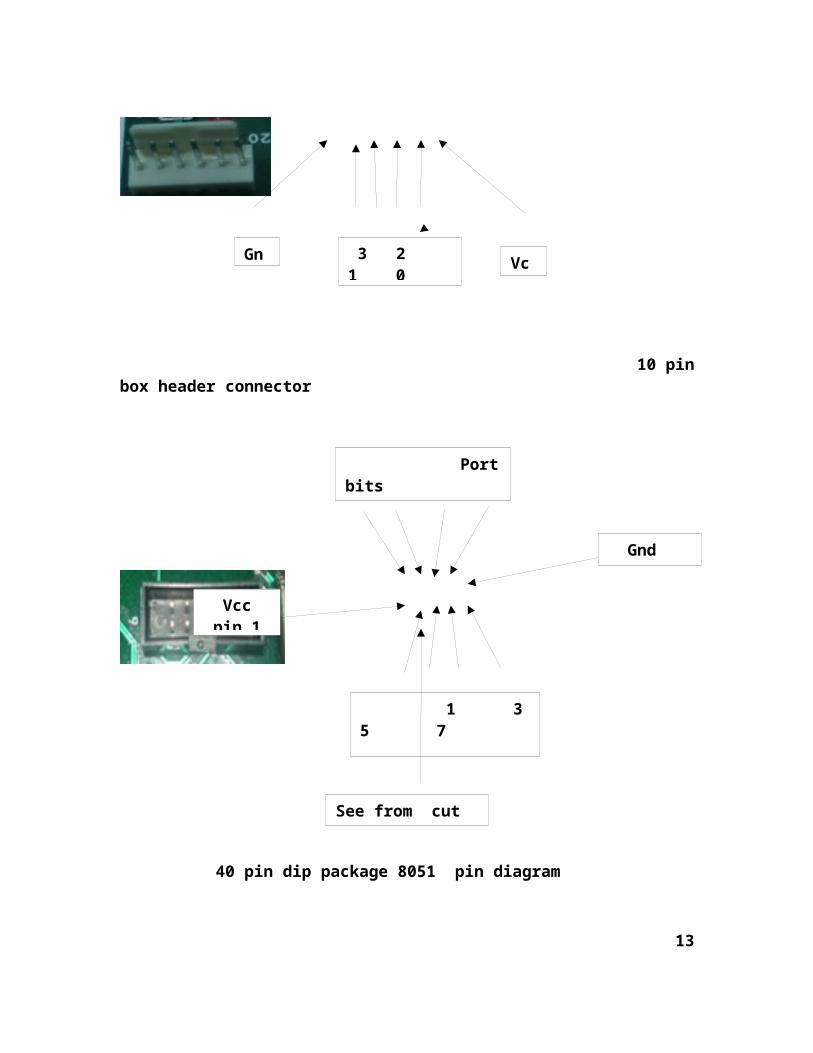
Pin details for on board 6 & 10 pin connectors, all 6 pin & 10 pin connectors available on hardware board are standard pin specified according to images shown below. 6 pin connector
Gn 3 2 1 0
Port bitsVcc
8

10 pin box header connector
40 pin dip package 8051 pin diagram
1 3 5 7 Port bits
Port bits 0 2 4 6
Vcc pin 1
Gnd pin 10
See from cut side
9
Block diagram for 8051
10

8051Microcontroller Board has on board
(a) ADC section.
(b) RTC & EEPROM section.
(c) DISPLAY (LCD, LED, & 7-SEG) section.
(d) INPUT SWITCHES (PUSH BUTTON & DIP SWITCH) section.
(e) RELAY section.
(f) BUZZER section
(g) RS232 SECTION
(h) 4X4 MATRIX KEYPAD SECTION
(i) POWER SUPPLY SECTION
(j) STEPPER MOTOR SECTION
(k) DAC SECTION
PERIPHERALS
Part No. Specifications
ADC0809CCN 8-BIT 8-CHANNEL, 100s.RTC DS1307 64X8, SERIAL I2C Real Time Clock.EPROM 24C04 4K serial EEPROM.LCD 16 x 2 character LCDBUZZER 5VRELAY 5A/250V ACDAC0808 8 bit+12vdc,-15v dcSTEPPER MOTOR 5 V7-SEGMENT COMMON ANODELED 1.5V
POWER SUPPLY REQUIREMENTS
Voltage Rating Current Rating
+/- 5 V 1A+/- 12V 1A
11
8051 Microcontroller Board Features
P89C51RD2/P89V51RD2 Features• On-chip Flash Program Memory with In-System Programming (ISP) and In-Application Programming (IAP) capability• Boot ROM contains low-level Flash programming routines for downloading via the UART• Can be programmed by the end-user application (IAP)• Parallel programming with 87C51 compatible hardware interface to programmer• Supports 6-clock/12-clock mode via parallel programmer (default clock mode after Chip Erase is 12-clock)• 6-clock/12-clock mode Flash bit erasable and programmable via ISP• 6-clock/12-clock mode programmable “on-the-fly” by SFR bit• Peripherals (PCA, timers, UART) may use either 6-clock or 12-clock mode while the CPU is in 6-clock mode• Speed up to 20 MHz with 6-clock cycles per machine cycle (40 MHz equivalent performance); up to 33 MHz with 12 clocks per machine cycle• Fully static operation• RAM expandable externally to 64 Kbytes• Four interrupt priority levels• Seven interrupt sources• Four 8-bit I/O ports• Full-duplex enhanced UART
– Framing error detection– Automatic address recognition
• Power control modes– Clock can be stopped and resumed– Idle mode– Power down mode
• Programmable clock-out pin• Second DPTR register• Asynchronous port reset• Low EMI (inhibit ALE)• Programmable Counter Array (PCA)
– PWM– Capture/compare
12
KEY BOARD SECTIONKey board is an input section with 4 switches to give input to microcontroller.with use of keyboard section we can put conditions on microcontroller to give or not give output. In this section a 6 pin connector is provided to connect with microcontroller any port .From right first pin is +5v dc(Vcc),second to fourth are switch select pin,with each pin switch is connected,from left first pin is ground(GND).
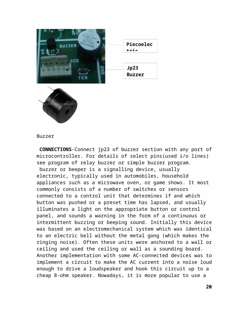
KEY BOARD Different types of key switches BUZZER SECTION
A Buzzer is output device having +ve and –ve terminals ,which generate a tone when it get high signal on its positive terminal.these devices are capable of geneate sound ,such kind of devices can be used in hardwares like security systems and sensitive equipments to protect them from burn.For example if temperature of particular area rise over than prespecified temperature then a sound should generate.
Buzzer
Piecoelectric buzzer
Jp23 Buzzer input connector
Key board connector External intrupt
13

CONNECTIONS-Connect jp23 of buzzer section with any port of microcontroller. For details of select pins(used i/o lines) see program of relay buzzer or simple buzzer program. buzzer or beeper is a signalling device, usually electronic, typically used in automobiles, household appliances such as a microwave oven, or game shows. It most commonly consists of a number of switches or sensors connected to a control unit that determines if and which button was pushed or a preset time has lapsed, and usually illuminates a light on the appropriate button or control panel, and sounds a warning in the form of a continuous or intermittent buzzing or beeping sound. Initially this device was based on an electromechanical system which was identical to an electric bell without the metal gong (which makes the ringing noise). Often these units were anchored to a wall or ceiling and used the ceiling or wall as a sounding board. Another implementation with some AC-connected devices was to implement a circuit to make the AC current into a noise loud enough to drive a loudspeaker and hook this circuit up to a cheap 8-ohm speaker. Nowadays, it is more popular to use a ceramic-based piezoelectric sounder which makes a high-pitched tone. Usually these were hooked up to "driver" circuits which varied the pitch of the sound or pulsed the sound on and off.
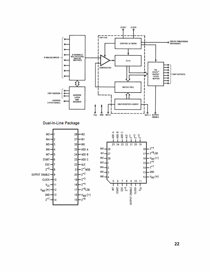
ANALOG TO DIGITAL CONVERTER (ADC0809)
ADC General Description:
The ADC0809 Data acquisition component is a monolithic CMOS device with an 8-bit analog-to-digital converter, 8 channel multiplexer and microprocessor compatible control logic. The 8-bit A/D converter uses successive approximation as the conversion technique. The converter features a high impedance chopper stabilized comparator, a 256R voltage divider with analog switch tree and a successive approximation register. The 8-bit Channel multiplexer can directly access any of 8 segnal-ended analog signals.The device eliminates the need for external zero and full scale adjustments. Easey interfacing to microprocessors input and latched TTL TRI-STATE output.The design of the ADC0808,ADC0809 has been optimized by incorporating the most desirable aspects of several A/D conversion techniques. The ADC0808, ADC0809 offers high speed, high accuracy, minimal temperature dependence, excellent long term accuracy and repeatability, and consumes minimal power. These features make this device ideally suited to application from process and machine control to consumer and automotive application. For 16-channel multiplexer with common output (sample/hold port) see ADC0816 data sheet. (See AN274 for more information.)
14

15

CIRCUIT DIAGRAM FOR ADC
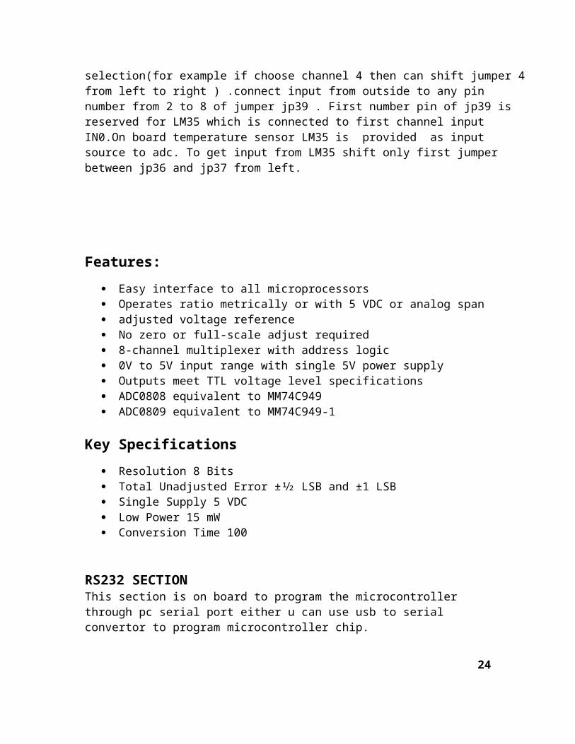
8 varaiable resistors are provided in adc section , each is connected to channel input. IN0,IN1,IN2,IN3.IN4,IN5,IN6,IN7 to give input to adc .Either input can give from out side by shifting jumpers between jp36 and jp37 from 1 to 8( left to right ).jumpers can be selected optionally according to channel selection(for example if choose channel 4 then can shift jumper 4 from left to right ) .connect input from outside to any pin number from 2 to 8 of jumper jp39 . First number pin of jp39 is reserved for LM35 which is connected to first channel input IN0.On board temperature sensor LM35 is provided as input source to adc. To get input from LM35 shift only first jumper between jp36 and jp37 from left.
ADC 0809
Jp 31 SET0 SET1 SET2 CLK 0 1 2 3
Jp 28 EOC ALE SOC OE 4 5 6 7
Jp 26 8 bit digital out
LM 35 temperature sensor
Input to 8 channels IN0 IN1 IN2 IN3 IN4 IN5 IN6 IN7
16

Features:
Easy interface to all microprocessors Operates ratio metrically or with 5 VDC or analog span adjusted voltage reference No zero or full-scale adjust required 8-channel multiplexer with address logic 0V to 5V input range with single 5V power supply Outputs meet TTL voltage level specifications ADC0808 equivalent to MM74C949 ADC0809 equivalent to MM74C949-1
Key Specifications
Resolution 8 Bits Total Unadjusted Error ±1⁄2 LSB and ±1 LSB Single Supply 5 VDC Low Power 15 mW Conversion Time 100
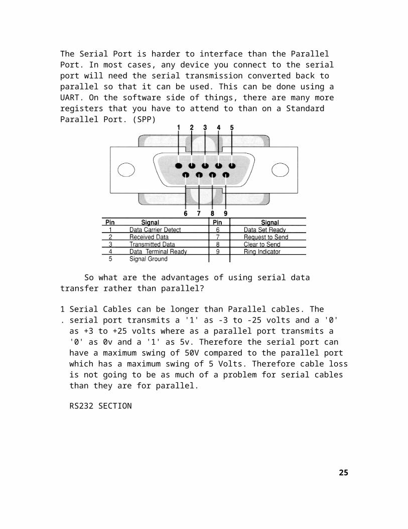
RS232 SECTIONThis section is on board to program the microcontroller through pc serial port either u can use usb to serial convertor to program microcontroller chip.The Serial Port is harder to interface than the Parallel Port. In most cases, any device you connect to the serial port will need the serial transmission converted back to parallel so that it can be used. This can be done using a UART. On the software side of things, there are many more registers that you have to attend to than on a Standard Parallel Port. (SPP)
So what are the advantages of using serial data transfer rather than parallel?
17

1. Serial Cables can be longer than Parallel cables. The serial port transmits a '1' as -3 to -25 volts and a '0' as +3 to +25 volts where as a parallel port transmits a '0' as 0v and a '1' as 5v. Therefore the serial port can have a maximum swing of 50V compared to the parallel port which has a maximum swing of 5 Volts. Therefore cable loss is not going to be as much of a problem for serial cables than they are for parallel.
RS232 SECTION
2. You don't need as many wires than parallel transmission. If your device needs to be mounted a far distance away from the computer then 3 core cable (Null Modem Configuration) is going to be a lot cheaper that running 19 or 25 core cable. However you must take into account the cost of the interfacing at each end.
3. Infra Red devices have proven quite popular recently. You may of seen many electronic diaries and palmtop computers which have infra red capabilities build in. However could you imagine transmitting 8 bits of data at the one time across the room and being able to (from the devices point of view) decipher which bits are which? Therefore serial transmission is used where one bit is sent at a time. IrDA-1 (The first infra red specifications) was capable of 115.2k baud and was interfaced into a UART. The pulse length however was cut down to 3/16th of a RS232 bit length to conserve power considering these devices are mainly used on diaries, laptops and palmtops.
4. Microcontroller's have also proven to be quite popular recently. Many of these have in built SCI (Serial Communications Interfaces) which can be used to talk to the outside world. Serial Communication reduces the pin count of these MPU's. Only two pins are commonly used, Transmit Data (TXD) and Receive Data (RXD) compared with at least 8 pins if you use a 8 bit Parallel method (You may also require a Strobe).
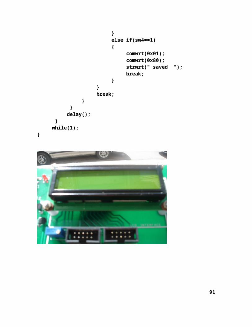
LCD DISLAY SECTION
9 pin D connector to program 8051
18

A liquid crystal display (LCD) is a thin, flat panel used for electronically displaying information such as text, images, and moving pictures. Its uses include monitors for computers, televisions, instrument panels, and other devices ranging from aircraft cockpit displays, to every-day consumer devices such as video players, gaming devices, clocks, watches, calculators, and telephones. Among its major features are its lightweight construction, its portability, and its ability to be produced in much larger screen sizes than are practical for the construction of cathode ray tube (CRT) display technology. Its low electrical power consumption enables it to be used in battery-powered electronic equipment. It is an electronically-modulated optical device made up of any number of pixels filled with liquid crystals and arrayed in front of a light source (backlight) or reflector to produce images in color or monochrome. The earliest discoveries leading to the development of LCD technology date from 1888. By 2008, worldwide sales of televisions with LCD screens had surpassed the sale of CRT units.
JP2 8 bit data port
Jp44 4 bit data port
Jp5 2 bit control rs & eJp 31 2 bit control rs & e
19
CONNECTIONS- Connect any port of 8051(carrying data) from microcontroller with jp2(in case of 8 bit data mode )and with jp44(in case of 4 bit data mode) data port of lcd (D0-D7) and control port with jp5(0-RS and 1-E) or jp31(0-RS and 1-E) of lcd.For more details see program of lcd display. FEATURES• 5 x 8 dots with cursor• Built-in controller (KS 0066 or Equivalent)• + 5V power supply (Also available for + 3V)• 1/16 duty cycle• B/L to be driven by pin 1, pin 2 or pin 15, pin 16 or A.K (LED)• N.V. optional for + 3V power supply
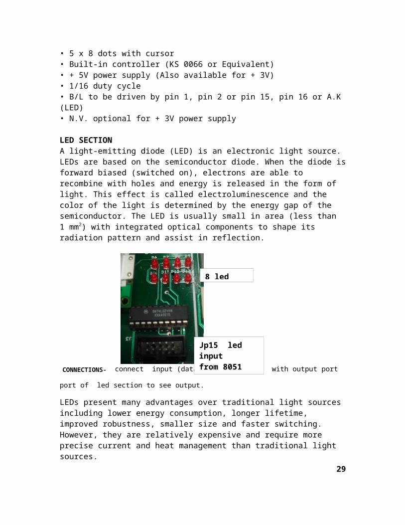
LED SECTIONA light-emitting diode (LED) is an electronic light source. LEDs are based on the semiconductor diode. When the diode is forward biased (switched on), electrons are able to recombine with holes and energy is released in the form of light. This effect is called electroluminescence and the color of the light is determined by the energy gap of the semiconductor. The LED is usually small in area (less than 1 mm2) with integrated optical components to shape its radiation pattern and assist in reflection.
Jp15 led input from 8051
8 led display
20

CONNECTIONS- connect input (data) port from 8051 with output port port of led section to see
output.
LEDs present many advantages over traditional light sources including lower energy consumption, longer lifetime, improved robustness, smaller size and faster switching. However, they are relatively expensive and require more precise current and heat management than traditional light sources.
Applications of LEDs are diverse. They are used as low-energy indicators but also for replacements for traditional light sources in general lighting and automotive lighting. The compact size of LEDs has allowed new text and video displays and sensors to be developed, while their high switching rates are useful in communications technology.
SEVEN SEGMENT DISLAY SECTION
A seven-segment display -less commonly known as a seven-segment indicator, is a form of electronic display device for displaying decimal numerals that is an alternative to the more complex dot-matrix displays. Seven-segment displays are widely used in digital clocks, electronic meters, and other electronic devices for displaying numerical information.
Concept and visual structure -The individual segments of a seven-segment display.A seven segment display, as its name indicates, is composed of seven elements. Individually on or off, they can be combined to produce simplified representations of the arabic numerals. Often the seven segments are arranged in an oblique, or italic, arrangement, which aids readability.
Each of the numbers 0, 6, 7 and 9 may be represented by two or more different glyphs on seven-segment displays.
21
CONNECTIONS- connect data carrying port of 8051 with jp21 data port of 7 segment section and control port with jp13 of seven segment section to see output.
The seven segments are arranged as a rectangle of two vertical segments on each side with one horizontal segment on the top, middle, and bottom. Additionally, the seventh segment bisects the rectangle horizontally. There are also fourteen-segment displays and sixteen-segment displays (for full alphanumerics); however, these have mostly been replaced by dot-matrix displays.
The segments of a 7-segment display are referred to by the letters A to G, as shown to the right, where the optional DP decimal point (an "eighth segment") is used for the display of non-integer numbers.
RELAY SECTION
A relay is an electrical switch that opens and closes under the control of another electrical circuit. In the original form, the switch is operated by an electromagnet to open or close one or many sets of contacts. It was invented by Joseph Henry in 1835. Because a relay is able to control an output circuit of higher power than the input circuit, it can be considered to be, in a broad sense, a form of an electrical amplifier.
Common anode 7 seg.
Jp13 control port
Jp21 data port
22

Relay
Jp27 input to relayGnd 3 2 1 0 Vcc
Jp 30 12v dc supply relay
NO C NC Jp24 relay 1 out
NO C NCJp32 relay 2 out
Gnd+12v
23
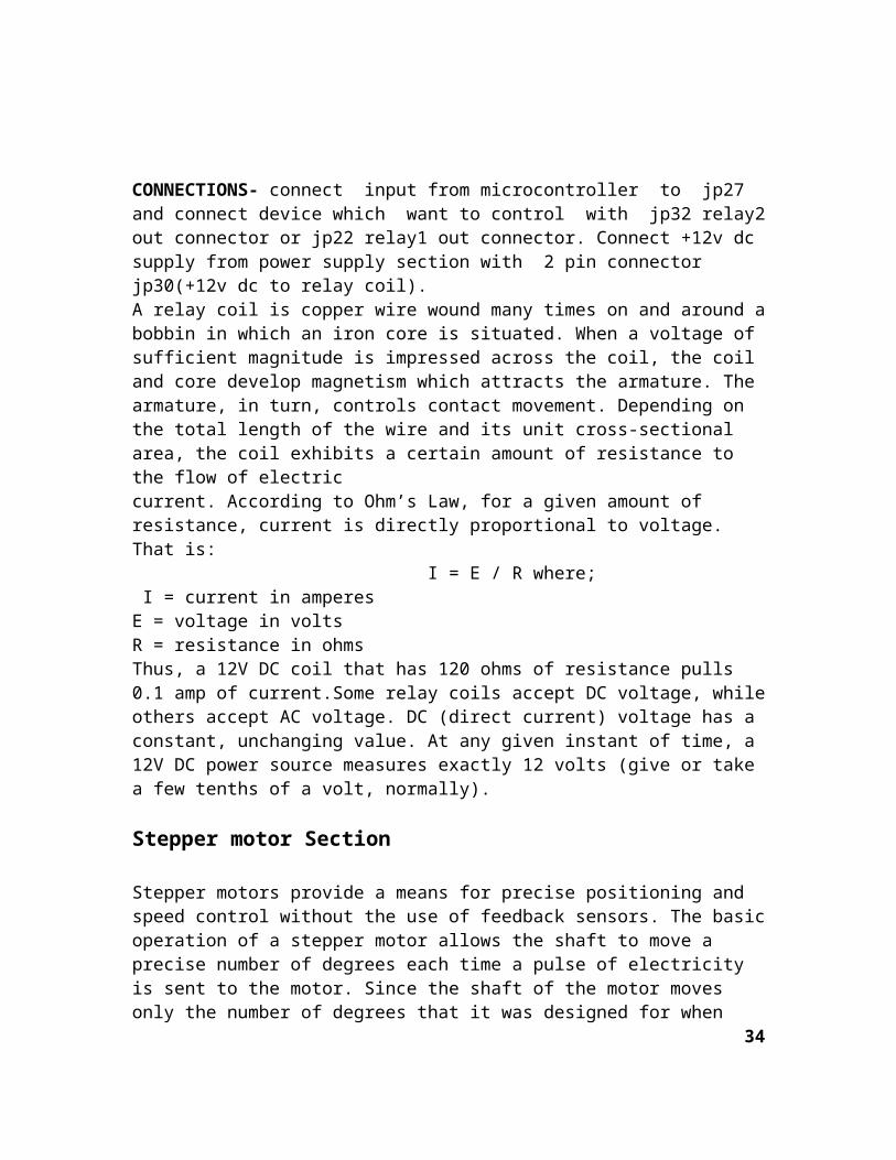
CONNECTIONS- connect input from microcontroller to jp27 and connect device which want to control with jp32 relay2 out connector or jp22 relay1 out connector. Connect +12v dc supply from power supply section with 2 pin connector jp30(+12v dc to relay coil).A relay coil is copper wire wound many times on and around a bobbin in which an iron core is situated. When a voltage of sufficient magnitude is impressed across the coil, the coil and core develop magnetism which attracts the armature. The armature, in turn, controls contact movement. Depending on the total length of the wire and its unit cross-sectional area, the coil exhibits a certain amount of resistance to the flow of electriccurrent. According to Ohm’s Law, for a given amount of resistance, current is directly proportional to voltage. That is: I = E / R where; I = current in amperesE = voltage in voltsR = resistance in ohmsThus, a 12V DC coil that has 120 ohms of resistance pulls 0.1 amp of current.Some relay coils accept DC voltage, while others accept AC voltage. DC (direct current) voltage has a constant, unchanging value. At any given instant of time, a 12V DC power source measures exactly 12 volts (give or take a few tenths of a volt, normally).
Stepper motor Section
Stepper motors provide a means for precise positioning and speed control without the use of feedback sensors. The basic operation of a stepper motor allows the shaft to move a precise number of degrees each time a pulse of electricity is sent to the motor. Since the shaft of the motor moves only the number of degrees that it was designed for when each pulse is delivered, you can control the pulses that are sent and control the positioning and speed. The rotor of the motor produces torque from the interaction between the magnetic field in the stator and rotor. The strength of the magnetic fields is proportional to the amount of current sent to the stator and the number of turns in the windings. The stepper motor uses the theory of operation for magnets to make the motor shaft turn a precise distance when a pulse of electricity is provided. You learned previously that like poles of a magnet repel and unlike poles attract. Figure 1 shows a typical cross-sectional view of the rotor and stator of a stepper motor. From this diagram you can see that the stator (stationary winding) has eight poles, and the rotor has six poles (three complete magnets). The rotor will require 24 pulses of electricity to move the 24 steps to make one complete revolution. Another way to say this is that the rotor will move precisely 15° for each pulse of electricity that the motor receives. The number of degrees the rotor will turn when a pulse of electricity is delivered to the motor can be calculated by dividing the number of degrees in one revolution of the shaft (360°) by the number of poles (north and south) in the rotor. In this stepper motor 360° is divided by 24 to get 15°. When no power is applied to the motor, the residual magnetism in the rotor magnets will cause the rotor to detent or align one set of its magnetic poles with the magnetic poles of one of the stator magnets. This means that the rotor will have 24 possible detent positions. When the rotor is in a detent position, it will have enough magnetic force to keep the shaft from moving
24
Jp128 bit input data from 8051
Jp16 Ouput to stepper motor
to the next position. This is what makes the rotor feel like it is clicking from one position to the next as you rotate the rotor by hand with no power applied.
Stepper motor fig 1.
Fig 1. Diagram that shows the position of the six-pole rotor and eight-pole stator of a typical stepper motor.
When power is applied, it is directed to only one of the stator pairs of windings, which will cause that winding pair to become a magnet. One of the coils for the pair will become the North Pole, and the other will become the South Pole. When this occurs, the stator coil that is the North Pole will attract the closest rotor tooth that has the opposite polarity, and the stator coil that is the South Pole will attract the closest rotor tooth that has the opposite polarity. When current is flowing through these poles, the rotor will now have a much stronger attraction to the stator winding, and the increased torque is called holding torque.
CIRCUIT DIAGRAM FOR STEPPER MOTOR
Jp128 bit input data from 8051
Jp16 Ouput to stepper motor
25

By changing the current flow to the next stator winding, the magnetic field will be changed 45°. The rotor will only move 15° before its magnetic fields will again align with the change in the stator field. The magnetic field in the stator is continually changed as the rotor moves through the 24 steps to move a total of 360°. Figure 2 shows the position of the rotor changing as the current supplied to the stator changes.
FIGURE 2. Movement of the stepper motor rotor as current is pulsed to the stator. (a) Current is applied to the A and A’ windings, so the A winding is north, (b) Current is applied to B and B’ windings, so the B winding is north, (c) Current is applied to the C and C’ windings, so the C winding is north, (d) Current is applied to the D and D’ windings so the D winding is north. (e) Current is applied to the A and A’ windings, so the A’ winding is north.
26

CONNECTIONS- Stepper motor section have two connectors, jp16 & jp12 .jp12 is input connector from microcontroller and jp16 is output connector to stepper motor.
DAC0808 SECTION
In electronics, a digital-to-analog converter (DAC or D-to-A) is a device for converting a digital (usually binary) code to an analog signal (current, voltage or electric charge).
A DAC converts an abstract finite-precision number (usually a fixed-point binary number) into a concrete physical quantity (e.g., a voltage or a pressure). In particular, DACs are often used to convert finite-precision time series data to a continually-varying physical signal.
A typical DAC converts the abstract numbers into a concrete sequence of impulses. that are then processed by a reconstruction filter using some form of interpolation to fill in data between the impulses. Other DAC methods (e.g., methods based on Delta-sigma modulation) produce a pulse-density modulated signal that can then be filtered in a similar way to produce a smoothly-varying signal.
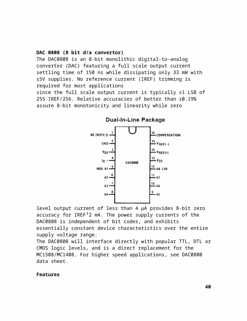
DAC 0808 (8 bit d/a convertor)The DAC0808 is an 8-bit monolithic digital-to-analog converter (DAC) featuring a full scale output current settling time of 150 ns while dissipating only 33 mW with ±5V supplies. No reference current (IREF) trimming is required for most applicationssince the full scale output current is typically ±1 LSB of 255 IREF/256. Relative accuracies of better than ±0.19% assure 8-bit monotonicity and linearity while zero
27

level output current of less than 4 μA provides 8-bit zero accuracy for IREF³2 mA. The power supply currents of the DAC0808 is independent of bit codes, and exhibits essentially constant device characteristics over the entire supply voltage range.The DAC0808 will interface directly with popular TTL, DTL or CMOS logic levels, and is a direct replacement for the MC1508/MC1408. For higher speed applications, see DAC0800 data sheet.
Features Relative accuracy: ±0.19% error maximum Full scale current match: ±1 LSB type Fast settling time: 150 ns typ Noninverting digital inputs are TTL and CMOS ompatible High speed multiplying input slew rate: 8 mA/μs Power supply voltage range: ±4.5V to ±18V Low power consumption: 33 mW @ ±5V
RTC & E2PROM
RTC A real-time clock (RTC) is a computer clock (most often in the form of an integrated circuit )that keeps track of the current time. Although the term often refers to the devices in personal computers, servers and embedded systems, RTCs are present in almost any electronic device which needs to keep accurate time. The DS1307 serial real-time clock (RTC) is alow-power, full binary-coded decimal (BCD) clock/calendar plus 56 bytes of NV SRAM. Address and data are transferred serially through an I2C*, bidirectional bus. The clock/calendar provides seconds, minutes, hours, day, date, month, and year information. The end of the month date is automatically adjusted for months with fewer than 31 days, including corrections for leap year. The clock operates in either
28
the 24- hour or 12-hour format with AM/PM indicator. The DS1307 has a built-in power-sense circuit that detects power failures and automatically switches to the battery supply.
RTC DS1307 FEATURES
Real-time clock (RTC) counts seconds, minutes, hours, date of the month, month, day of the week, and year with leap-year compensation valid up to 2100
56-byte, battery-backed, nonvolatile (NV) RAM for data storage Two-wire serial interface Programmable square wave output signal Automatic power-fail detect and switch circuitry Consumes less than 500nA in battery backup mode with oscillator
running Optional industrial temperature range: -40°C to +85°C Available in 8-pin DIP or SOIC Underwriters Laboratory (UL) recognized
E2PROM 24C04 FEATURES
Low-voltage and Standard-voltage Operation– 2.7 (VCC = 2.7V to 5.5V)– 1.8 (VCC = 1.8V to 5.5V)
Internally Organized 128 x 8 (1K), 256 x 8 (2K), 512 x 8 (4K), 1024 x 8 (8K) or 2048 x 8 (16K)
2-wire Serial Interface Schmitt Trigger, Filtered Inputs for Noise Suppression Bi-directional Data Transfer Protocol 100 kHz (1.8V) and 400 kHz (2.5V, 2.7V, 5V) Compatibility Write Protect Pin for Hardware Data Protection 8-byte Page (1K, 2K), 16-byte Page (4K, 8K, 16K) Write Modes Partial Page Writes are Allowed Self-timed Write Cycle (5 ms max) High-reliability
– Endurance: 1 Million Write Cycles– Data Retention: 100 Years
Automotive Grade, Extended Temperature and Lead-Free Devices Available
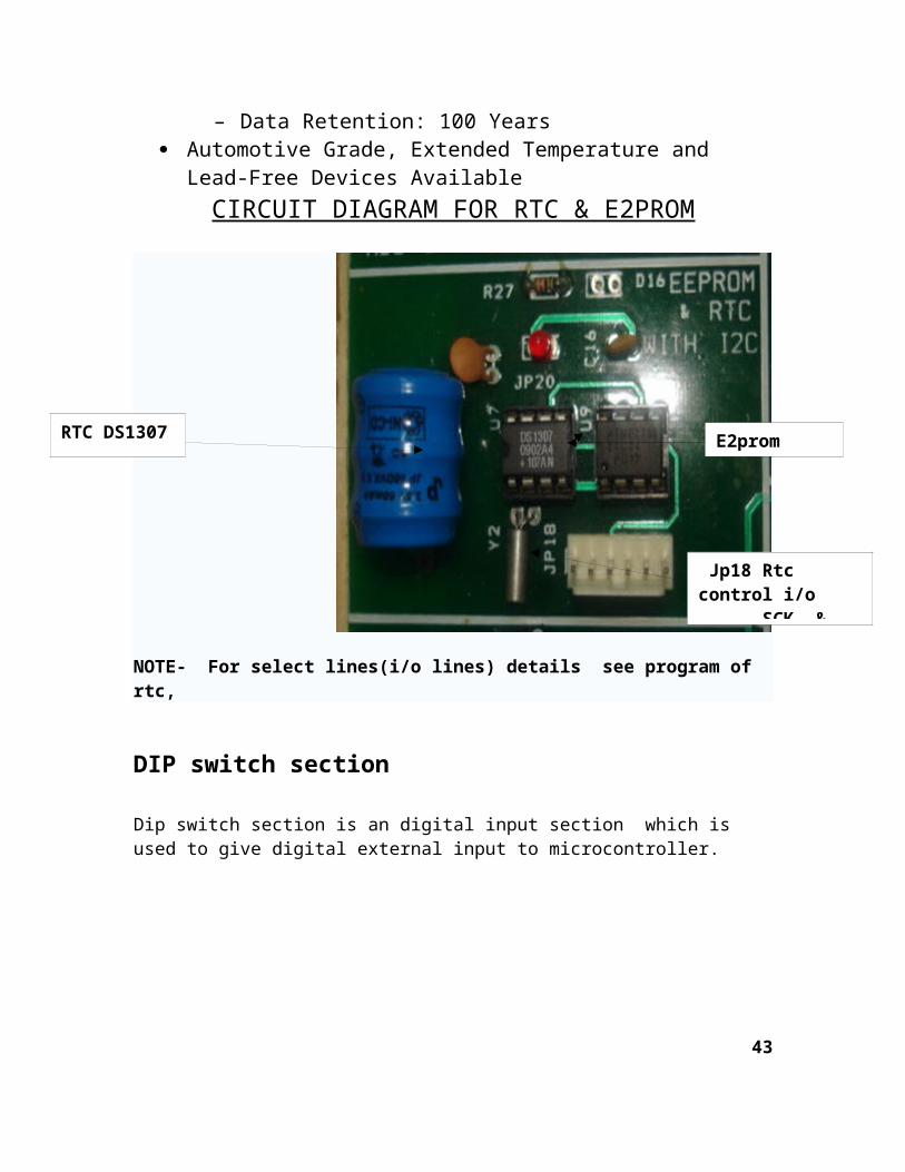
CIRCUIT DIAGRAM FOR RTC & E2PROM29

NOTE- For select lines(i/o lines) details see program of rtc,
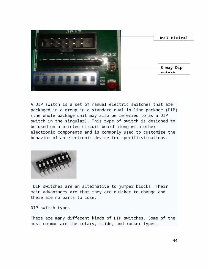
DIP switch section
Dip switch section is an digital input section which is used to give digital external input to microcontroller.
A DIP switch is a set of manual electric switches that are packaged in a group in a standard dual in-line package (DIP) (the whole package unit may also be referred to as a
E2prom 24c04 242224242424c
RTC DS1307
Jp18 Rtc control i/o SCK & SDATA
Jp17 Digital output
8 way Dip switch
30

DIP switch in the singular). This type of switch is designed to be used on a printed circuit board along with other electronic components and is commonly used to customize the behavior of an electronic device for specificsituations.
DIP switches are an alternative to jumper blocks. Their main advantages are that they are quicker to change and there are no parts to lose.
DIP switch types
There are many different kinds of DIP switches. Some of the most common are the rotary, slide, and rocker types.
Rotary DIP switches contain multiple contacts, one of which is selected by rotating the switch to align it with a number printed on the package.
The slide and rocker types, which are very common, are arrays of simple SPDT (single-pole, single-throw) contacts, which can be either on or off. This allows each switch to select a one-bit binary value. The values of all switches in the DIP package can also be interpreted as one number. For example, seven switches offer 128 combinations, allowing them to select a standard ASCII character. Eight switches offer 256 combinations, which is equivalent to one byte.
The DIP switch package also has socket pins or mounting leads to provide an electrical path from the switch contacts to the circuit board. Although circuits can use the electrical contacts directly, it is more common to convert them into high and low signals. In this case the circuit board also needs interface circuitry for the DIP switch, consisting of a series of pull-up or pull-down resistors, a buffer, decode logic, and other components. Typically the device's firmware reads the DIP switches. They were also often used on arcade games in the 1980s and early 1990s to store settings, before the advent of cheaper, battery-backed RAM and were very commonly used to set security codes on garage door openers as well as on some early cordless phones. This design, which used up to twelve switches in a group, was used to avoid interference from other nearby door opener remotes or other devices. Current garage door openers use rolling code systems for better security.
These type of switches were used on early video cards for early computers to facilitate compatibility with other video standards. For example, CGA cards allowed for MDA compatibility.
31

Recently (since the late 1990s), DIP switches have become less common in consumer electronics. Reasons include the trend toward smaller products, the demand for easier configuration through setting screens, and the falling price of non-volatile memory. But DIP switches are still widely used in industrial equipment because they are inexpensive and easy to incorporate into circuit designs, and because they allow settings to be checked at a glance without powering the system on.
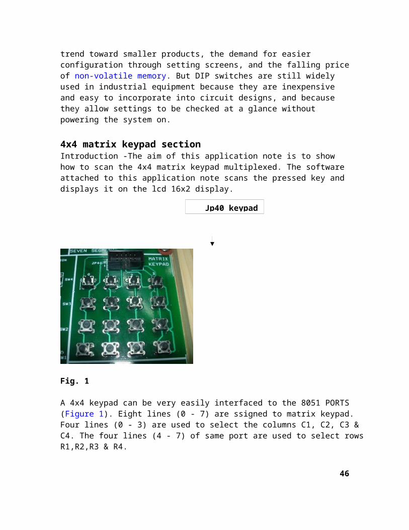
4x4 matrix keypad section Introduction -The aim of this application note is to show how to scan the 4x4 matrix keypad multiplexed. The software attached to this application note scans the pressed key and displays it on the lcd 16x2 display.
Fig. 1
A 4x4 keypad can be very easily interfaced to the 8051 PORTS (Figure 1). Eight lines (0 - 7) are ssigned to matrix keypad. Four lines (0 - 3) are used to select the columns C1, C2, C3 & C4. The four lines (4 - 7) of same port are used to select rows R1,R2,R3 & R4.
CONNECTIONS- Make connections for lcd display by connecting data and control port of 8051 and connect keypad connector jp40 with 8051 port(selected for keypad interface).for more details how to use see program of matrix keypad.
Jp40 keypad ouput
32

USE OF COMPILER
AND PROGRAMMER
Compiler: KEIL
Programming Tool: FLASH MAGIC
1. Double Click on the icon present on the desktop.
33
2. The following window will be popped-up
3. Go to the project & click on new project
34

4. Make a folder on desktop & give file name.
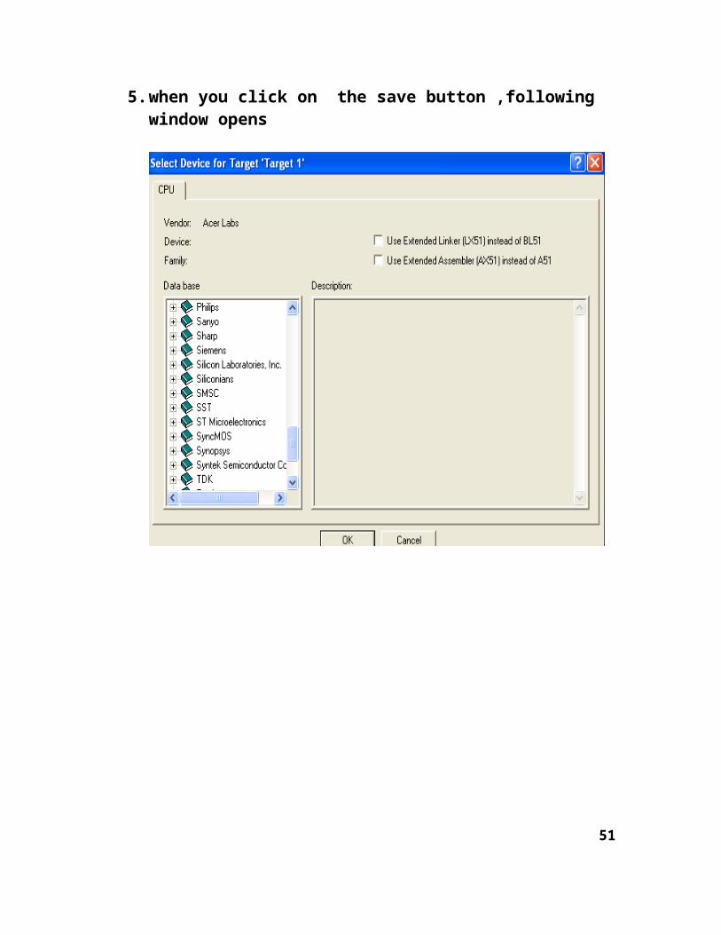
5. when you click on the save button ,following window opens
35

6. Select Philips & 89v51RD2xx
36

7. Then select NO on the pop-up given below.
8. Then make a New File.
37

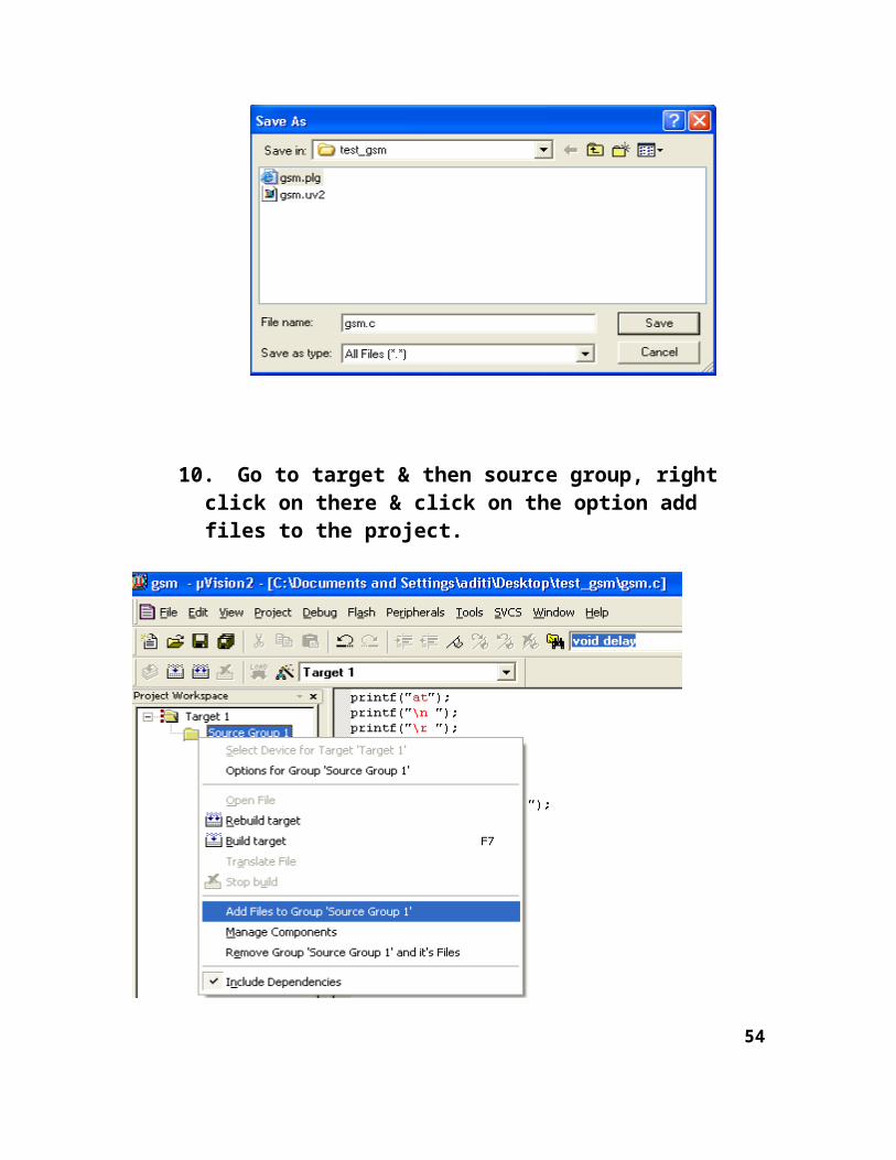
9. Write or copy your code there & save it with extension .c or .asm depending on your coding.
10.Go to target & then source group, right click on there & click on the option add files to the project.
38

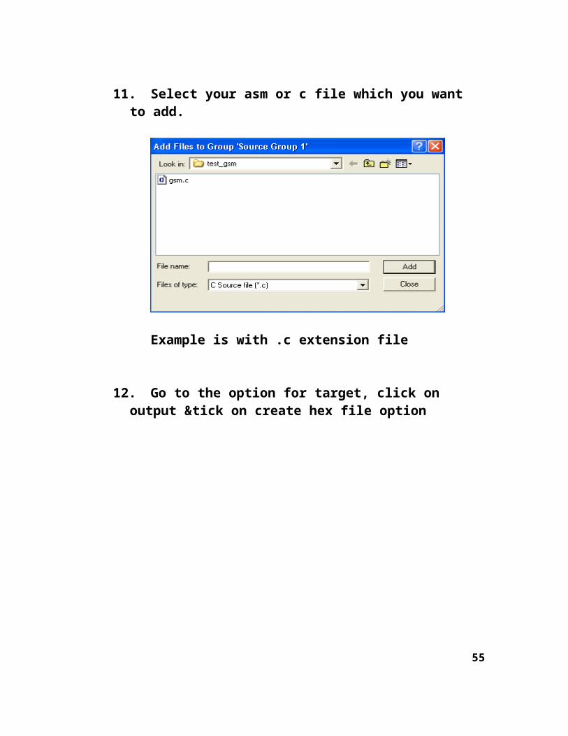
11.Select your asm or c file which you want to add.
Example is with .c extension file
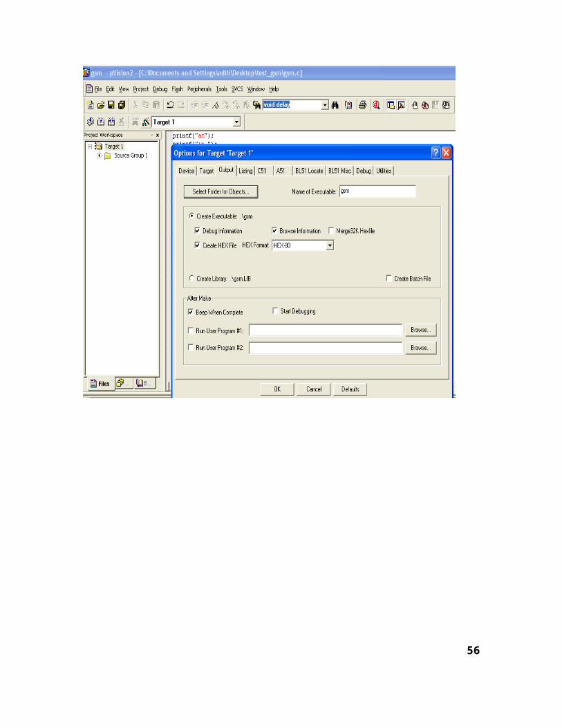
12.Go to the option for target, click on output &tick on create hex file option
39
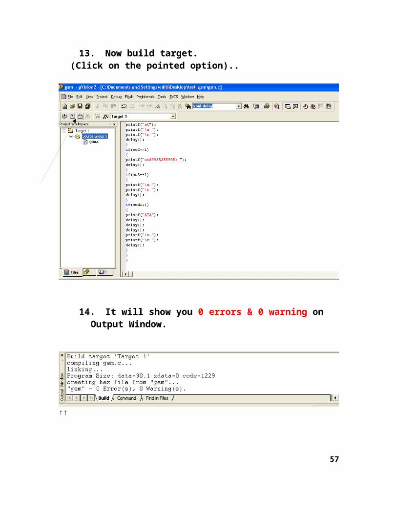
13.Now build target.(Click on the pointed option)..
40

14.It will show you 0 errors & 0 warning on Output Window.
↑↑
41

After performing all these steps the chip will be configured through Flash Magic .Let us hand on the steps of chip configuration through Flash Magic………
Special Notes: -
Make all the DIP switches in off position before burning the program in the controller.
Connect the Programming Cable on your Kit (prog. Conn.)And other side of cable with the COM Port of the Computer.
Burn the Program in the microcontroller with help of FLASH MAGIC or ECE FLASH as explained in the next section.
42
How to use FLASH-MAGICOR
How to use ECE flash
The following window will be popped-up
Press “cancel” to continue.
43
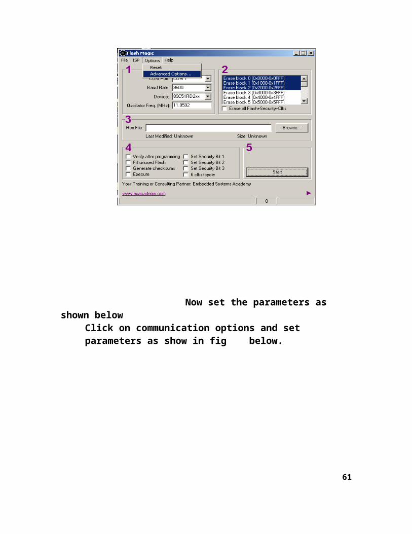
Configuration:Click options and then click advanced options…
Now set the parameters as shown belowClick on communication options and set parameters as show in fig below.
44
Click on hardware config and set parameters T1(200)and T2(300). Now disable option use DTR and RST shown in fig below.
45
Click on timeouts option and set parameters regular timeout 30, long timeout 120 and diasable option use my timeouts for ISP operations as shown in fig below.
46

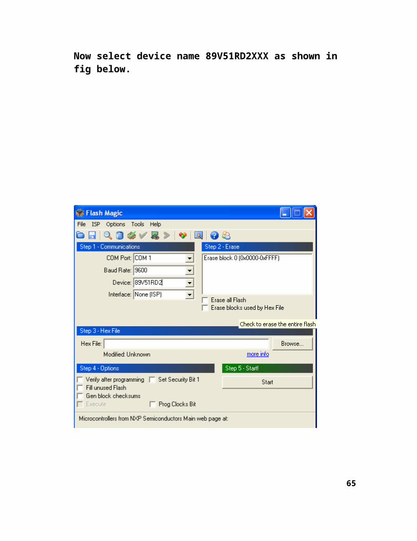
now click ok main front window will appear.Now select device name 89V51RD2XXX as shown in fig below.
47

After selection of the chip (P89v51RD2xx) , Port (Com1), Osc.Mhz(11.0592) we can see the window as below:
48

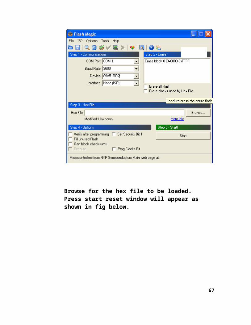
Browse for the hex file to be loaded. Press start reset window will appear as shown in fig below.
49

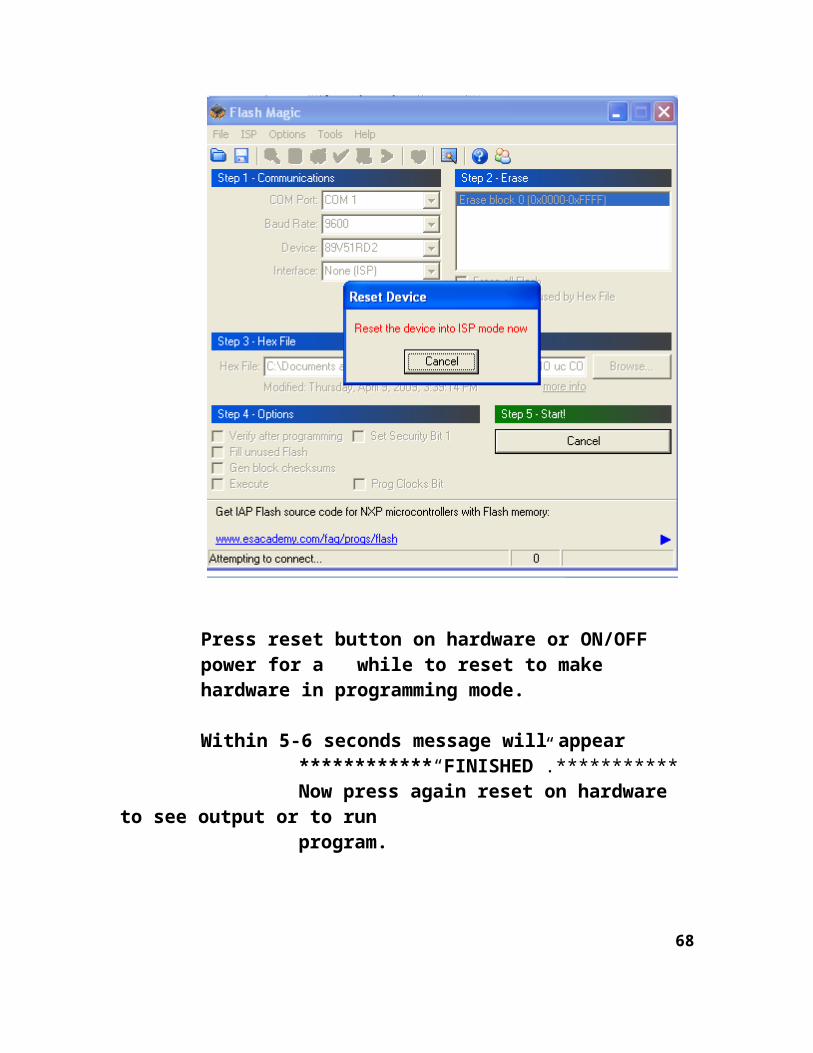
Press reset button on hardware or ON/OFF power for a while to reset to make hardware in programming mode.
Within 5-6 seconds message will appear ************“FINISHED”.*********** Now press again reset on hardware to see output or to run program.
50
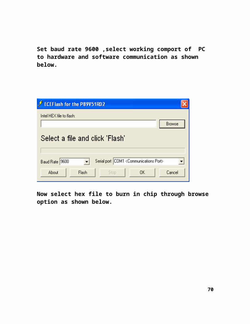
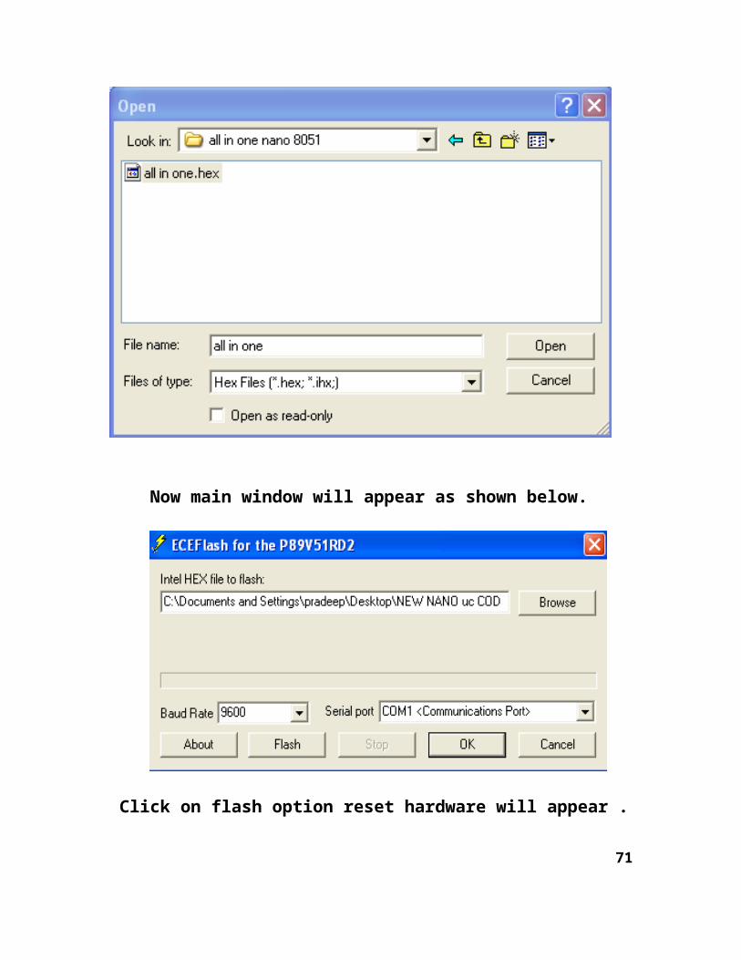
To burn chip 89V51RDRXX through ECE flash it required less .Double click on icon as shown below.
Flash window will appear as shown below.
Set baud rate 9600 ,select working comport of PC to hardware and software communication as shown below.
51

Now select hex file to burn in chip through browse option as shown below.
Now main window will appear as shown below.
52

Click on flash option reset hardware will appear .
Now press reset switch on hardware board and flash will burn with 5-6 Seconds.Again press reset switch on hardware board to run your program or to see output.
53
EXPERIMENTS FOR 8051
DAUGHTER BOARD
54
EXPERIMENT NO: 1
AIM: Program of right shift of LED’S
CONNECTIONS: Connect Port0 (P0) to LED Section.
//connect port0 to led section//# include<reg51.h>void delay();void main(){P0=0X01;delay();P0=0X02;delay();P0=0X04;delay();P0=0X08;delay();P0=0X10;delay();P0=0X20;delay();P0=0X40;delay();P0=0X80;delay();}
void delay(){int i;for(i=0;i<=30000;i++);}
55
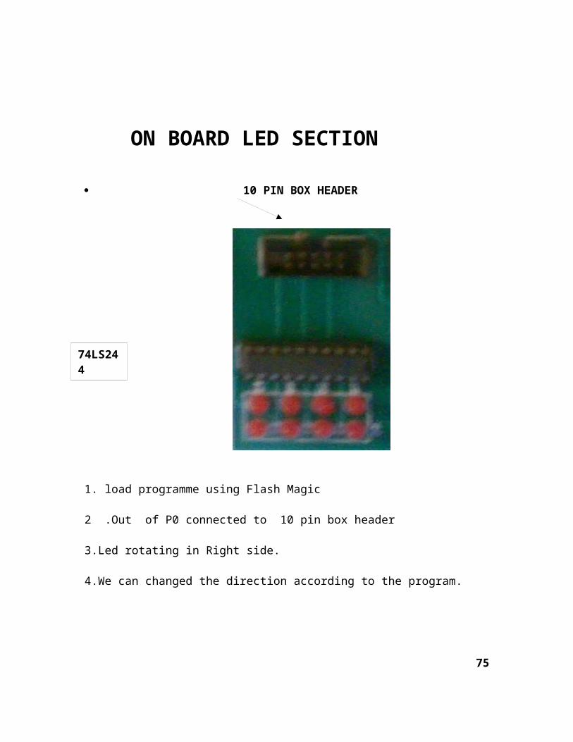
ON BOARD LED SECTION
10 PIN BOX HEADER
1. load programme using Flash Magic
2 .Out of P0 connected to 10 pin box header
3.Led rotating in Right side.
4.We can changed the direction according to the program.
74LS244
56
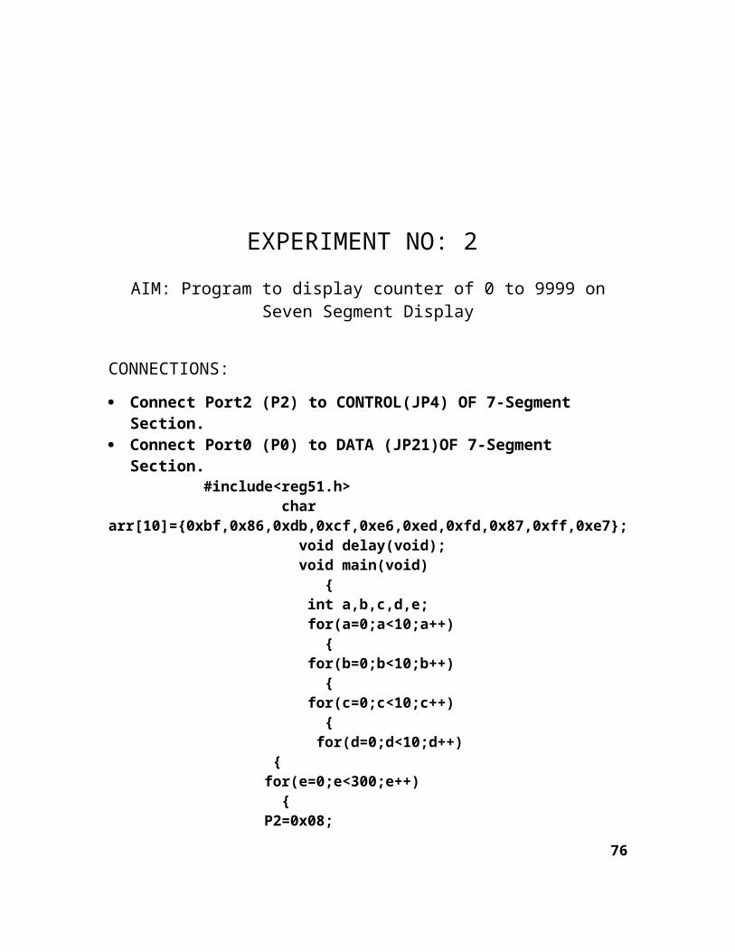
EXPERIMENT NO: 2
AIM: Program to display counter of 0 to 9999 on Seven Segment Display
CONNECTIONS:
Connect Port2 (P2) to CONTROL(JP4) OF 7-Segment Section. Connect Port0 (P0) to DATA (JP21)OF 7-Segment Section. #include<reg51.h> char arr[10]={0xbf,0x86,0xdb,0xcf,0xe6,0xed,0xfd,0x87,0xff,0xe7}; void delay(void); void main(void) { int a,b,c,d,e; for(a=0;a<10;a++) { for(b=0;b<10;b++) { for(c=0;c<10;c++) { for(d=0;d<10;d++)
{ for(e=0;e<300;e++) { P2=0x08; P0=arr[a]; delay(); P2=0x04; P0=arr[b]; delay(); P2=0x02; P0=arr[c]; delay(); P2=0x01; P0=arr[d]; delay(); } } } } } }
void delay(void) { int f;for(f=0;f<20;f++); }
57
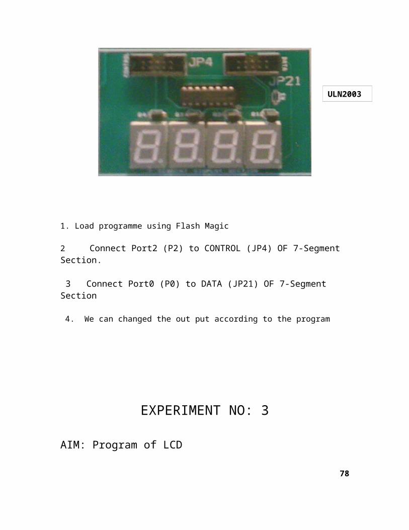
ON BOARD SEVEN SEGMENT
1. Load programme using Flash Magic
2 Connect Port2 (P2) to CONTROL (JP4) OF 7-Segment Section.
3 Connect Port0 (P0) to DATA (JP21) OF 7-Segment Section
4. We can changed the out put according to the program
EXPERIMENT NO: 3
Controlled Pins Data Pins
ULN2003
58

AIM: Program of LCD
CONNECTIONS:
Connect Port2 (P2) to JP2 OF LCD Section. Connect Port0 (P0) to JP5 OF LCD Section.
/////PORT0-----LCD CONTRL /////PORT2-----LCD DATA
#include<reg51.h>sbit RS=P0^0;sbit E=P0^1;void cmddiply(){RS=0;E=1;E=0;}void datadiply(){RS=1;E=1;E=0;}void delay(){int i;for(i=0;i<30000;i++);}void main(){while(1){P2=0x38;cmddiply();delay();P2=0x0E;cmddiply();delay();P2=0x06;cmddiply();
59

delay();P2=0x01;cmddiply();delay();P2=0x80;cmddiply();delay();
P2='A';datadiply();delay();P2='D';datadiply();delay();P2='V';datadiply();delay();P2='A';datadiply();delay();P2='N';datadiply();delay();P2='C';datadiply();delay();P2='E';datadiply();delay();P2=0xC0;cmddiply();delay();P2='T';datadiply();delay();P2='E';datadiply();delay();P2='C';datadiply();delay();P2='H';datadiply();delay();P2='8';datadiply();
60
delay();P2='5';datadiply();delay();P2='1';datadiply();delay();}}
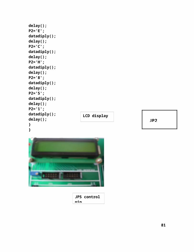
1. Load programme using Flash Magic
2 Connect Port2 (P2) to DATA (JP2) OF LCD
3 Connect Port0 (P0) to CONTROL (JP5) OF LCD
4. ADVANCE TECH851 display on Lcd
5 We can changed the out put according to the pr
EXPERIMENT NO: 4
AIM: Program for Dip Test
LCD display
JP2 data JP5 control pin
61

CONNECTIONS:
Connect Port2 (P2) to LED Section. Connect Port0 (P0) to DIP switch Section.
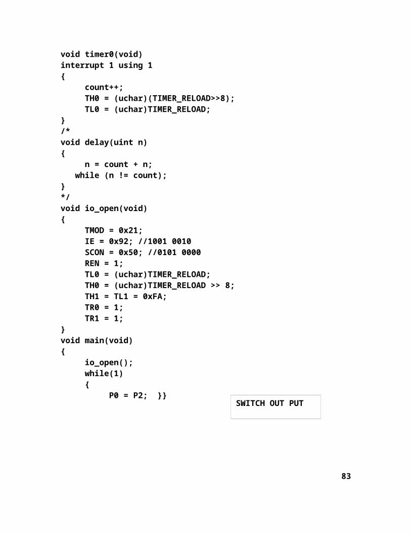
#include<reg51.h>#include<intrins.h>typedef unsigned char uchar;typedef unsigned long ulong;typedef unsigned int uint;#define TIMER_RELOAD (-921)#define port_delay() _nop_(), _nop_(), _nop_(), _nop_()uint count;ulong value;uchar state,rdata;void timer0(void)interrupt 1 using 1{
count++;TH0 = (uchar)(TIMER_RELOAD>>8);TL0 = (uchar)TIMER_RELOAD;
}/*void delay(uint n){
n = count + n; while (n != count);}*/void io_open(void){
TMOD = 0x21;IE = 0x92; //1001 0010SCON = 0x50; //0101 0000REN = 1;TL0 = (uchar)TIMER_RELOAD;TH0 = (uchar)TIMER_RELOAD >> 8;TH1 = TL1 = 0xFA;TR0 = 1;TR1 = 1;
}void main(void){
io_open();62

while(1){
P0 = P2; }}
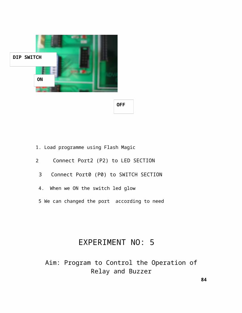
1. Load programme using Flash Magic
2 Connect Port2 (P2) to LED SECTION
3 Connect Port0 (P0) to SWITCH SECTION
4. When we ON the switch led glow
5 We can changed the port according to need
EXPERIMENT NO: 5
Aim: Program to Control the Operation of Relay and Buzzer
DIP SWITCH
ON
OFF
SWITCH OUT PUT
63

CONNECTIONS:
Connect Port2 (P2) to RELAY & BUZZER Section.
#include<reg51.h>void delay(int);sbit rly1=P2^1;sbit rly2=P2^2;sbit buz=P2^3;main(){buz=1;rly1=1;delay(30000);rly1=0;delay(30000);buz=0;delay(30000);buz=1;rly2=1;delay(30000);rly2=0;buz=0;delay(30000);
}void delay(int x){int i;for(i=0;i<=x;i++);
EXPERIMENT NO:6
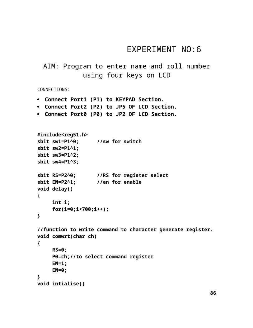
AIM: Program to enter name and roll number using four keys on LCD
CONNECTIONS:
64
Connect Port1 (P1) to KEYPAD Section. Connect Port2 (P2) to JP5 OF LCD Section. Connect Port0 (P0) to JP2 OF LCD Section.
#include<reg51.h>sbit sw1=P1^0; //sw for switchsbit sw2=P1^1;sbit sw3=P1^2;sbit sw4=P1^3;
sbit RS=P2^0; //RS for register selectsbit EN=P2^1; //en for enablevoid delay(){
int i;for(i=0;i<700;i++);
}
//function to write command to character generate register.void comwrt(char ch){
RS=0;P0=ch;//to select command registerEN=1;EN=0;
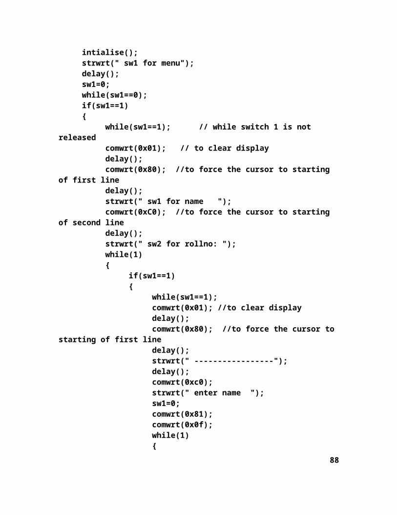
}void intialise(){
comwrt(0x38); //2 lines and 5*7 matrixdelay();comwrt(0x0c); //display on ,cursor not blinkingdelay();comwrt(0x01); //clear display
delay();comwrt(0x06); // to set entry modedelay();comwrt(0x80); //force cursor to beginning of 1st linedelay();
}
//function to write the data into data display register.void datawrt(char ch){
RS=1; //to select data display register
65

P0=ch;EN=1; //for high to low pulseEN=0;
}
//function to display a string on LCDvoid strwrt(char *ptr){
int i;for(;*ptr!='\0';ptr++){
datawrt(*ptr);delay();for(i=0;i<25;i++)delay();
}}void main(){
char i=0,l=0; // i for alphabet number and l for location on LCDintialise();strwrt(" sw1 for menu");delay();sw1=0;while(sw1==0);if(sw1==1){
while(sw1==1); // while switch 1 is not releasedcomwrt(0x01); // to clear displaydelay();comwrt(0x80); //to force the cursor to starting of first linedelay();strwrt(" sw1 for name ");comwrt(0xC0); //to force the cursor to starting of second linedelay();strwrt(" sw2 for rollno: ");while(1){
if(sw1==1){
while(sw1==1);comwrt(0x01); //to clear displaydelay();comwrt(0x80); //to force the cursor to starting of
first linedelay();
66
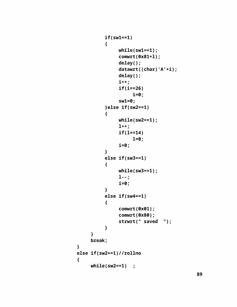
strwrt(" -----------------");delay();comwrt(0xc0);strwrt(" enter name ");sw1=0;comwrt(0x81);comwrt(0x0f);while(1){
if(sw1==1){
while(sw1==1);comwrt(0x81+l);delay();datawrt((char)'A'+i);delay();i++;if(i==26)
i=0;sw1=0;
}else if(sw2==1){
while(sw2==1);l++;if(l==14)
l=0;i=0;
}else if(sw3==1){
while(sw3==1);l--;i=0;
}else if(sw4==1){
comwrt(0x01);comwrt(0x80);strwrt(" saved ");
}}break;
}else if(sw2==1)//rollno{
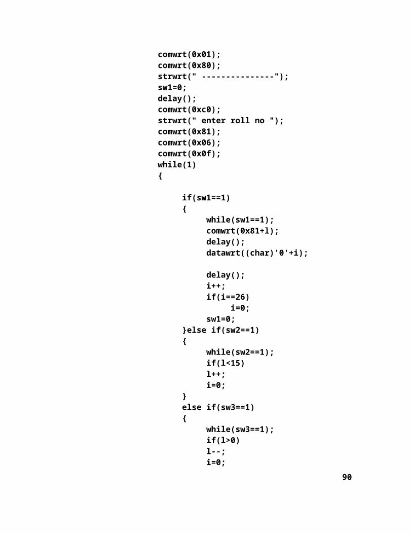
67
while(sw2==1) ;comwrt(0x01);comwrt(0x80);strwrt(" ---------------");sw1=0;delay();comwrt(0xc0);strwrt(" enter roll no ");comwrt(0x81);comwrt(0x06);comwrt(0x0f);while(1){
if(sw1==1){
while(sw1==1);comwrt(0x81+l);delay();datawrt((char)'0'+i);
delay();i++;if(i==26)
i=0;sw1=0;
}else if(sw2==1){
while(sw2==1);if(l<15)l++;i=0;
}else if(sw3==1){
while(sw3==1);if(l>0)l--;i=0;
}else if(sw4==1){
comwrt(0x01);comwrt(0x80);strwrt(" saved ");break;
68

}}break;
} }delay();
}while(1);
}
EXPERIMENT NO: 7
AIM: PROGRAM OF ANALOG TO DIGITAL CONVERTER
CONNECTIONS:
Connect Port3 (P3) to ADC Section.69
Connect Port2 (P2) to JP2 OF LCD Section. Connect Port0 (P0) to JP5 OF LCD Section. Connect Port1 (P1) to 8-bit digital data OF ADC Section.
#include<reg52.h>#include<intrins.h>
typedef unsigned char uchar;typedef unsigned long ulong;typedef unsigned int uint;
#define TIMER_RELOAD (-921)#define port_delay() _nop_(), _nop_(), _nop_(), _nop_()
sbit LRS = P0 ^ 0;sbit LEN = P0 ^ 1;sbit OE = P1 ^ 7;sbit SOC = P1 ^ 6;sbit ALE1 = P1 ^ 5;sbit EOC = P1 ^ 4;sbit ADC_CLK = P1 ^ 3;sbit SEL0 = P1 ^ 2;sbit SEL1 = P1 ^ 1;sbit SEL2 = P1 ^ 0;
uint count,value;uchar adc_val,state;
void timer0(void)interrupt 1 using 1{
count++;TH0 = (uchar)(TIMER_RELOAD>>8);TL0 = (uchar)TIMER_RELOAD;ADC_CLK = ~ADC_CLK;
}
void delay(uint n){
n = count + n; while (n != count);}
void dispstr(uchar *str, uchar stcol, uchar encol)
70
{ uint q;
if(stcol <= 15)P2 = 0x80 + stcol;
elseP2 = 0xB0 + stcol;
LRS = 0;LEN = 1;
LEN = 0; delay(1);
LRS = 1;q=0;for(; stcol <= encol; stcol++){
if(stcol == 16){
P2 = 0xB0 + stcol;LRS = 0;LEN = 1;
LEN = 0;delay(1);LRS = 1;
}P2 = str[q];q++;LEN = 1;
LEN = 0;delay(1);
}}
void clrlcd(){
LRS = 0;P2 = 0x01;LEN = 1;LEN = 0;delay(6);
}
void io_open(void){
LEN = 0;TMOD = 0x21;
71

IE = 0x92; //1001 0010TL0 = (uchar)TIMER_RELOAD;TH0 = (uchar)TIMER_RELOAD >> 8;TR0 = 1;
}
void initlcd(void){
LEN = 0;LRS = 0;delay(20);
P2 = 0x30; LEN = 1; delay(1); LEN = 0; delay(6); P2 = 0x30; LEN = 1; delay(1); LEN = 0; delay(6);
P2 = 0x30; LEN = 1; delay(1); LEN = 0; delay(6);
P2 = 0x38; //funtion set LEN = 1; delay(1); LEN = 0; delay(6);
P2 = 0x0c8; //display off LEN = 1; delay(1); LEN = 0; delay(6);
P2 = 0x01; //clear display; LEN = 1; delay(1); LEN = 0;
72

delay(6);
P2 = 0x06; //entry mode set LEN = 1; delay(1); LEN = 0; delay(6);
P2 = 0x0c; //display on LEN = 1;
delay(1); LEN = 0; delay(6);
}
void dispnum(uint no, uchar stcol, uchar encol) {
uchar temp[5];uchar i,k;for (i = 0; i < 5; i++){
temp[i] = no % 10;no /= 10;
}if(stcol <= 15)
P2 = 0x80 + stcol;else
P2 = 0xB0 + stcol;LRS = 0;LEN = 1;
LEN = 0; delay(1);
LRS = 1;i = k = 4;for(; stcol <= encol; stcol++){
if( k == 1){
k = 200;dispstr(".",stcol,stcol);
}else{
P2 = temp[i] + 0x30;i--;
73

k--;LEN = 1;
LEN = 0;delay(1);
}}
}
void read_adc(void){
ALE1 = 1;OE = 0;SOC = 1;ALE1 = 0;SOC = 0;delay(100);while(!EOC);OE = 1;adc_val = P3;
}
void main(void){
io_open(); initlcd();
clrlcd ();dispstr(" ADVANCE ",0,15);delay(2000);state = 0;while(1){
switch(state){
case 0:dispstr("CHANNEL1 ",0,15);SEL0 = 0; SEL1 = 0; SEL2 = 0;read_adc();value = (adc_val * 400) /255;dispnum(value,16,21);delay(3000);state = 1;break;
case 1:dispstr("CHANNEL2 ",0,15);SEL0 = 0; SEL1 = 0; SEL2 = 1;
74
read_adc();value = (adc_val * 400) /255;dispnum(value,16,21);delay(3000);state = 2;break;
case 2:dispstr("CHANNEL3 ",0,15);SEL0 = 0; SEL1 = 1; SEL2 = 0;read_adc();value = (adc_val * 400) /255;dispnum(value,16,21);delay(3000);state = 3;break;
case 3:dispstr("CHANNEL4 ",0,15);SEL0 = 0; SEL1 = 1; SEL2 = 1;read_adc();value = (adc_val * 400) /255;dispnum(value,16,21);delay(3000);state = 0;break;
}}
}
PRESET
JUMPERSETTINGSECTION 75
1. Load programme using Flash Magic 2 Connect Port3 (P3) to ADC CONTROLE SECTION
3 Connect Port2 (P2) to JP2 OF LCD Section. 4 Connect Port0 (P0) to JP5 OF LCD Section.
5 Connect Port1 (P1) to 8-bit digital data OF ADC Section. 6 Out put display ON LCD
EXPERIMENT NO: 8AIM: PROGRAM OF REAL TIME CONTROL
CONNECTIONS:
Connect Port1 (P1) to RTC Section. Connect Port2 (P2) to JP2 OF LCD Section. Connect Port0 (P0) to JP5 OF LCD Section.
#include<reg51.h>#include<intrins.h>
ADC DATA OUTADC CONTROL
EXTERNAL INPUT
INTERNAL INPUT
76

typedef unsigned char uchar;typedef unsigned long ulong;typedef unsigned int uint;
#define TIMER_RELOAD (-921)#define port_delay() _nop_(), _nop_(), _nop_(), _nop_()#define AVG 10
sbit LRS = P0 ^ 0;sbit LEN = P0 ^ 1;sbit ICLK = P1 ^ 3;sbit IDAT = P1 ^ 1;
uint count;uchar rdata,edata;uint time;uchar second,minute,hour,day,date,month,year;
void timer0(void)interrupt 1 using 1{
count++;TH0 = (uchar)(TIMER_RELOAD>>8);TL0 = (uchar)TIMER_RELOAD;
}
void delay(uint n){
n = count + n; while (n != count);}
void dispstr(uchar *str, uchar stcol, uchar encol) { uint q;
if(stcol <= 15)P2 = 0x80 + stcol;
elseP2 = 0xB0 + stcol;
LRS = 0;LEN = 1;
LEN = 0; delay(1);
LRS = 1;77
q=0;for(; stcol <= encol; stcol++){
if(stcol == 16){
P2 = 0xB0 + stcol;LRS = 0;LEN = 1;
LEN = 0;delay(1);LRS = 1;
}P2 = str[q];q++;LEN = 1;
LEN = 0;delay(1);
}}
void dispnum(uint no, uchar stcol, uchar encol) {
uchar temp[5];uchar i;for (i = 0; i < 2; i++){
temp[i] = no % 10;no /= 10;
}if(stcol <= 15)
P2 = 0x80 + stcol;else
P2 = 0xB0 + stcol;LRS = 0;LEN = 1;
LEN = 0; delay(1);
LRS = 1;i = 1;for(; stcol <= encol; stcol++){
P2 = temp[i] + 0x30;i--;LEN = 1;
LEN = 0;78
delay(1);}
}
void clrlcd(){
LRS = 0;P2 = 0x01;LEN = 1;LEN = 0;delay(6);
}
void str1307(void){ IDAT = 1 ; _nop_() , _nop_() , _nop_() ; ICLK = 1 ; _nop_() , _nop_() , _nop_() ; IDAT = 0 ; _nop_() , _nop_() , _nop_() ; ICLK = 0 ; _nop_() , _nop_() , _nop_() ;}
void stp1307(void){ IDAT = 0 ; _nop_() , _nop_() , _nop_() ; ICLK = 1 ; _nop_() , _nop_() , _nop_() ; IDAT = 1 ; _nop_() , _nop_() , _nop_() ; ICLK = 0 ; _nop_() , _nop_() , _nop_() ;}
void clock(void){ _nop_() ; _nop_() ; _nop_() ; ICLK = 1 ; _nop_() ; _nop_() ; _nop_() ; ICLK = 0 ; _nop_() ; _nop_() ; _nop_() ;}
79

void ack1307(void){ IDAT = 0 ; clock() ;}
void nack1307(void){ IDAT = 1 ; clock() ;}
void opdat(char rtcdata){ char i ; for ( i = 0 ; i < 8 ; i++ ) { if ( ( rtcdata >> ( 7 - i ) ) & 0x01 ) IDAT = 1 ; else
IDAT = 0 ; clock() ; }}
void waitack(void){// watch() ; IDAT = 1 ; _nop_() , _nop_() , _nop_() ; while ( IDAT ) ; ICLK = 1 ; _nop_() , _nop_() , _nop_() ; ICLK = 0 ;}
char getdat(void){ char i , dat ;// watch() ; IDAT = 1 ; _nop_() , _nop_() , _nop_() ; for ( i = 0 ; i < 8 ; i++ ) { ICLK = 1 ; dat = ( ( ( dat << 1 ) & 0xfe ) | IDAT ) ;
_nop_() , _nop_() , _nop_() ;80
ICLK = 0 ; _nop_() , _nop_() , _nop_() ; } return dat ;}
/*void gortc(void) { str1307() ; opdat(0xd0) ; waitack() ; opdat(0x07); waitack(); opdat(0x90); waitack(); stp1307();}*/
void getrtc(void){ char rdata ;// watch() ; str1307() ; opdat(0xd0) ; waitack() ; opdat(0x00) ; waitack() ; stp1307() ; _nop_() , _nop_() , _nop_() ; str1307() ; opdat(0xd1) ; waitack() ; rdata = getdat() ; ack1307() ;
second = ( rdata & 0x7f) ; rdata = getdat() ; ack1307() ;
minute = ( rdata & 0x7f) ; rdata = getdat() ; ack1307() ;
hour = ( rdata & 0x3f) ; rdata = getdat() ; ack1307() ;// watch() ;
81

day = ( rdata & 0x07) ; rdata = getdat() ; ack1307() ;
date = ( rdata & 0x3f) ; rdata = getdat() ; ack1307() ;
month = ( rdata & 0x1f) ; rdata = getdat() ; nack1307() ;
year = rdata ; stp1307() ;}
void setrtc(void){ char rdata ;// watch() ; str1307() ; opdat(0xd0) ; waitack() ; opdat(0x00) ; waitack() ; rdata = ( second & 0x7f) ; opdat(rdata) ; waitack() ; rdata = ( minute & 0x7f) ; opdat(rdata) ; waitack() ; rdata = ( hour & 0x3f) ; opdat(rdata) ; waitack() ; rdata = ( day & 0x07) ; opdat(rdata); waitack(); rdata = ( date & 0x3f); opdat(rdata) ; waitack() ; rdata = ( month & 0x1f); opdat(rdata); waitack() ; rdata = year ; opdat(rdata) ; waitack() ; stp1307() ;}
82
unsigned char bcdtime(unsigned char x){ return ( ( ( x / 10 ) << 4 ) + ( x % 10 ) ) ;}
unsigned char binarytime(unsigned char x){ return ( ( ( x >> 4 ) * 10 ) + ( x & 0xf ) ) ;}
void getrtc1(void){ getrtc() ;// watch() ; year = binarytime( year ); month = binarytime( month ); date = binarytime( date ); hour = binarytime( hour ); minute = binarytime( minute ); second = binarytime( second );}
void setrtc1(void){ // watch() ; year = bcdtime( year ) ; month = bcdtime( month ) ; date = bcdtime( date ) ; hour = bcdtime( hour ) ; minute = bcdtime( minute ) ; second = bcdtime( second ) ; setrtc() ;}
/*void initrtc1(void){// gortc();// getrtc(); setrtc1();// watch();/* year = binarytime( year ); month = binarytime( month ); date = binarytime( date ); hour = binarytime( hour ); minute = binarytime( minute );
83
second = binarytime( second ); getrtc1(); setrtc1();} */
void io_open(void){
LEN = 0;TMOD = 0x21;IE = 0x92; //1001 0010SCON = 0x50; //0101 0000REN = 1;TL0 = (uchar)TIMER_RELOAD;TH0 = (uchar)TIMER_RELOAD >> 8;TH1 = TL1 = 0xFA;TR0 = 1;TR1 = 1;
}
void initlcd(void){
LEN = 0;LRS = 0;delay(20);
P2 = 0x30; LEN = 1; delay(1); LEN = 0; delay(6); P2 = 0x30; LEN = 1; delay(1); LEN = 0; delay(6);
P2 = 0x30; LEN = 1; delay(1); LEN = 0; delay(6);
P2 = 0x38; //funtion set LEN = 1;
84

delay(1); LEN = 0; delay(6); P2 = 0x0c8; //display off LEN = 1; delay(1); LEN = 0; delay(6);
P2 = 0x01; //clear display; LEN = 1; delay(1); LEN = 0; delay(6);
P2 = 0x06; //entry mode set LEN = 1; delay(1); LEN = 0; delay(6);
P2 = 0x0c; //display on LEN = 1;
delay(1); LEN = 0; delay(6);
}
void main(void){
io_open();initlcd();clrlcd ();dispstr(" ADVANCE ",0,15);delay(2000);minute = 52;hour = 3;second = 1;date = 18;month = 5;year = 4;
setrtc1();85
// getrtc1();dispstr(":",18,18);dispstr(":",21,21);while(1){
getrtc1();dispnum(hour,16,17);dispnum(minute,19,20);dispnum(second,22,23);
}}
EXPERIMENT NO: 9
AIM: PROGRAM TO CONTROL THE OPERATION OF STEPPER MOTOR
CONNECTIONS:
Connect Port2 (P2) to STEPPER MOTOR Section.
#include<reg51.h>#include<intrins.h>
typedef unsigned char uchar;
86

typedef unsigned long ulong;typedef unsigned int uint;
#define TIMER_RELOAD (-921)
uint count;
void timer0(void)interrupt 1 using 1{ count++;
TH0 = (uchar)(TIMER_RELOAD>>8);TL0 = (uchar)TIMER_RELOAD;
}
void delay(uint n){
n = count + n; while (n != count);}
void io_open(void){
TMOD = 0x21;IE = 0x92; //1001 0010SCON = 0x50; //0101 0000REN = 1;TL0 = (uchar)TIMER_RELOAD;TH0 = (uchar)TIMER_RELOAD >> 8;TH1 = TL1 = 0xFA;TR0 = 1;TR1 = 1;
} void positive_step(void){ P2 = 0x11;
delay(100);P2 = 0x22; delay(100);P2 = 0x44;delay(100);P2 = 0x88;delay(100);
}
void negative_step(void)87
{ P2 = 0x41;
delay(40);P2 = 0x82;delay(40);P2 = 0x28;delay(40);P2 = 0x14;delay(40);
}void left_90(void){ P2 = 0x44;
delay(40);P2 = 0x88;delay(40);P2 = 0x22;delay(40);P2 = 0x11;delay(40);
}void right_90(void){ P2 = 0x88;
delay(40);P2 = 0x44;delay(40);P2 = 0x22;delay(40);P2 = 0x11;delay(40);
}void forward(uchar step){
uchar i;for(i = 0;i < step;i++){
positive_step();}
}void back(uchar step){
uchar i;for(i = 0;i < step;i++){
88
negative_step();}
}void left(uchar step){
uchar i;for(i = 0;i < step;i++){
left_90();}
}void right(uchar step){
uchar i;for(i = 0;i < step;i++){
right_90();}
}void main(void){
io_open();while(1){
forward(25);//right(20);
//forward(25);//left(20);
}/*forward(28);while(1);*/
}
89
1. Load programme using Flash Magic 2. Connect Port2 (P2) to STEPPER MOTOR Section
3. Motor speed and direction change according to programe
EXPERIMENT NO.10
AIM: PROGRAM TO CONTROL THE OPERATION OF TRAFFICE LIGHT
CONNECTION: P2 and P0 connected to traffic light module
//P2 and p0 with the connectors
STEPPER MOTOR OUTPUT
STEPPER MOTOR INPUT
ULN2003
90
org 00htraffic:;mov p2,#00h
; mov p0,#00h;acall delay
traffic_again:mov p2,#0dbhmov p0,#0aeh
acall delay mov p2,#0ddh
mov p0,#0eehacall delay1
mov p2,#09ehmov p0,#0ebh
acall delaymov p2,#0dehmov p0,#0edhacall delay1
mov p2,#076hmov p0,#0eeh
acall delaymov p2,#0eehmov p0,#0eehacall delay1
mov p2,#0dehmov p0,#05eh
acall delaymov p2,#0dehmov p0,#0f6hacall delay1
jmp traffic_again
delay1:mov r3,#0ffhloop4: mov r4,#0ffhloop3: mov r5,#08hloop5: djnz r5,loop5
djnz r4,loop3djnz r3,loop4
retdelay: mov r3,#0ffhloop1: mov r4,#0ffhloop2: mov r5,#01fhloop: djnz r5,loop
91

djnz r4,loop2djnz r3,loop1
retend
92