user manual rom-db5900 -...
TRANSCRIPT

User Manual
ROM-DB5900
Development Board for SMARC v1.0 modules

CopyrightThe documentation and the software included with this product are copyrighted 2014by Advantech Co., Ltd. All rights are reserved. Advantech Co., Ltd. reserves the rightto make improvements in the products described in this manual at any time withoutnotice. No part of this manual may be reproduced, copied, translated or transmittedin any form or by any means without the prior written permission of Advantech Co.,Ltd. Information provided in this manual is intended to be accurate and reliable. How-ever, Advantech Co., Ltd. assumes no responsibility for its use, nor for any infringe-ments of the rights of third parties, which may result from its use.
AcknowledgementsARM is trademarks of ARM Corporation.
Freescale is trademarks of Freescale Corporation.
Microsoft Windows are registered trademarks of Microsoft Corp.
All other product names or trademarks are properties of their respective owners.
Product Warranty (2 years)Advantech warrants to you, the original purchaser, that each of its products will befree from defects in materials and workmanship for two years from the date of pur-chase.
This warranty does not apply to any products which have been repaired or altered bypersons other than repair personnel authorized by Advantech, or which have beensubject to misuse, abuse, accident or improper installation. Advantech assumes noliability under the terms of this warranty as a consequence of such events.
Because of Advantech’s high quality-control standards and rigorous testing, most ofour customers never need to use our repair service. If an Advantech product is defec-tive, it will be repaired or replaced at no charge during the warranty period. For out-of-warranty repairs, you will be billed according to the cost of replacement materials,service time and freight. Please consult your dealer for more details.
If you think you have a defective product, follow these steps:
1. Collect all the information about the problem encountered. (For example, CPU speed, Advantech products used, other hardware and software used, etc.) Note anything abnormal and list any onscreen messages you get when the problem occurs.
2. Call your dealer and describe the problem. Please have your manual, product, and any helpful information readily available.
3. If your product is diagnosed as defective, obtain an RMA (return merchandize authorization) number from your dealer. This allows us to process your return more quickly.
4. Carefully pack the defective product, a fully-completed Repair and Replacement Order Card and a photocopy proof of purchase date (such as your sales receipt) in a shippable container. A product returned without proof of the purchase date is not eligible for warranty service.
5. Write the RMA number visibly on the outside of the package and ship it prepaid to your dealer.
Part No. 2006B59000 Edition 1
Printed in Taiwan June 2014
ROM-DB5900 User Manual ii

Declaration of Conformity
FCC Class B
Note: This equipment has been tested and found to comply with the limits for a ClassB digital device, pursuant to part 15 of the FCC Rules. These limits are designed toprovide reasonable protection against harmful interference in a residential installa-tion. This equipment generates, uses and can radiate radio frequency energy and, ifnot installed and used in accordance with the instructions, may cause harmful inter-ference to radio communications. However, there is no guarantee that interferencewill not occur in a particular installation. If this equipment does cause harmful interfer-ence to radio or television reception, which can be determined by turning the equip-ment off and on, the user is encouraged to try to correct the interference by one ormore of the following measures:
Reorient or relocate the receiving antenna. Increase the separation between the equipment and receiver. Connect the equipment into an outlet on a circuit different from that to which the
receiver is connected. Consult the dealer or an experienced radio/TV technician for help.
iii ROM-DB5900 User Manual

Warnings, Cautions and Notes
Packing ListBefore installation, please ensure the following items have been shipped.
Optional Accessories
Warning! Warnings indicate conditions, which if not observed, can cause personal injury!
Caution! Cautions are included to help you avoid damaging hardware or losing data. e.g.
There is a danger of a new battery exploding if it is incorrectly installed. Do not attempt to recharge, force open, or heat the battery. Replace the battery only with the same or equivalent type recommended by the man-ufacturer. Discard used batteries according to the manufacturer's instructions.
Note! Notes provide optional additional information.
9696M59000E SMARC v1.0 Carrier board ROM-DB5900 1
9696ED2000E debug adapter board 1
1700021882-01 LVDS backlight cable 1
1700021883-01 LVDS cable 1
1700021941-01 SATA power 1
1700004711 SATA signal 1
1700019076 USB OTG to Type A female 1
1700019077 USB OTG to Type A male 1
1701100300F Cable IDE#3 10P-2.54/D-SUB 9P(M) 30cm for UART and CAN
2
1700022840-01 SPDIF to RCA cable for audio in and out 1
1700022373-01 Debug port cable for ROM-5420 1
1700019474 A Cable D-SUB 9P(F)/D-SUB 9P(F) RS232/RS485 100c 1
2026M59000 China RoHS ROM-DB5900 Electronic Pollution 1st 1
Part No. Description
9696MEG510E Daughter board for audio codec
9696MEG500E Daughter board for MIPI camera
9680015487 Camera 5M MIPI I/F CCM module HAC-002005-B3A
9680015491 PCIe to miniPCIe adapter card
96LEDK-A070WV40NB1
7" LCD AUO G070VW01 V0 w/o tough
ROM-DB5900 User Manual iv

SMARC CPU Boards
For more information please refer to "Advantech Baseboard Check List" and "Evalu-ation Board Reference Schematic".
You can download "Advantech Baseboard Check List" and "Evaluation Board Refer-ence Schematic" from http://com.advantech.com/
Safety Instructions1. Read these safety instructions carefully.2. Keep this User Manual for later reference.3. Disconnect this equipment from any AC outlet before cleaning. Use a damp
cloth. Do not use liquid or spray detergents for cleaning.4. For plug-in equipment, the power outlet socket must be located near the equip-
ment and must be easily accessible.5. Keep this equipment away from humidity.6. Put this equipment on a reliable surface during installation. Dropping it or letting
it fall may cause damage.7. The openings on the enclosure are for air convection. Protect the equipment
from overheating. DO NOT COVER THE OPENINGS.8. Make sure the voltage of the power source is correct before connecting the
equipment to the power outlet.9. Position the power cord so that people cannot step on it. Do not place anything
over the power cord.10. All cautions and warnings on the equipment should be noted.11. If the equipment is not used for a long time, disconnect it from the power source
to avoid damage by transient overvoltage.12. Never pour any liquid into an opening. This may cause fire or electrical shock.13. Never open the equipment. For safety reasons, the equipment should be
opened only by qualified service personnel.14. If one of the following situations arises, get the equipment checked by service
personnel:The power cord or plug is damaged.Liquid has penetrated into the equipment.The equipment has been exposed to moisture.The equipment does not work well, or you cannot get it to work according to
the user's manual.The equipment has been dropped and damaged.The equipment has obvious signs of breakage.
15. DO NOT LEAVE THIS EQUIPMENT IN AN ENVIRONMENT WHERE THE STORAGE TEMPERATURE MAY GO BELOW -20° C (-4° F) OR ABOVE 60° C (140° F). THIS COULD DAMAGE THE EQUIPMENT. THE EQUIPMENT SHOULD BE IN A CONTROLLED ENVIRONMENT.
16. CAUTION: DANGER OF EXPLOSION IF BATTERY IS INCORRECTLY REPLACED. REPLACE ONLY WITH THE SAME OR EQUIVALENT TYPE
Part No. Description
ROM-5420CD-MDA1E Freescale i.mx6 Dual core 1GHz with 1GB memory (0~60C)
v ROM-DB5900 User Manual

RECOMMENDED BY THE MANUFACTURER, DISCARD USED BATTERIES ACCORDING TO THE MANUFACTURER'S INSTRUCTIONS.
The sound pressure level at the operator's position according to IEC 704-1:1982 isno more than 70 dB (A).
DISCLAIMER: This set of instructions is given according to IEC 704-1. Advantechdisclaims all responsibility for the accuracy of any statements contained herein.
Safety Precaution - Static ElectricityFollow these simple precautions to protect yourself from harm and the products fromdamage.
To avoid electrical shock, always disconnect the power from your PC chassis before you work on it. Don't touch any components on the CPU card or other cards while the PC is on.
Disconnect power before making any configuration changes. The sudden rush of power as you connect a jumper or install a card may damage sensitive elec-tronic components.
ROM-DB5900 User Manual vi

Contents
Chapter 1 General Introduction ...........................11.1 Introduction ............................................................................................... 21.2 Product Specification ................................................................................ 2
Chapter 2 H/W Installation....................................32.1 Module Form Factor.................................................................................. 42.2 Environmental Specifications .................................................................... 42.3 ROM-DB5900 Looks ................................................................................. 4
2.3.1 ROM-DB5900 Overview ............................................................... 42.3.2 I/O Connectors.............................................................................. 5
2.4 Connector, Jumper setting, Switch and LED ............................................ 52.4.1 Rear I/O panel............................................................................... 5
Table 2.1: External IO Connector ................................................ 5Table 2.2: DCIN1 (DC-Jack, +12V power input).......................... 5Table 2.3: CN16A (UART0, 2 wires) ........................................... 6Table 2.4: CN16B (UART2, 4 wires) ........................................... 6Table 2.5: VGA1 (VGA) ............................................................... 7Table 2.6: CN42 (HDMI).............................................................. 7Table 2.7: CN5 (RJ-45 & USB 1/2).............................................. 8Table 2.8: Audio1 (Audio output)................................................. 9
2.4.2 Internal I/O .................................................................................... 9Table 2.9: Internal IO Connector ................................................. 9
2.4.3 Connectors.................................................................................. 12Table 2.10:CN6 (PCIex1 connector1) ........................................ 12Table 2.11:CN7 (PCIex1 connector2) ........................................ 13Table 2.12:CN8 (PCIex1 connector3) ........................................ 14Table 2.13:CN11 (SATA connector)........................................... 15Table 2.14:CN12 (SATA Power connector)................................ 15Table 2.15:CN41 (CN41A, MXM 3.0 connector) ........................ 16Table 2.16:LVDS1 (LVDS 24bit)................................................. 19Table 2.17:LVDS_BK_PWR1 (LVDS backlight power) .............. 20Table 2.18:USB_OTG1 (USB OTG)........................................... 20Table 2.19:SD1 (SD slot)............................................................ 20Table 2.20:BAT1 (Lithium-ion Battery power input).................... 21Table 2.21:BH1 (CR-2032)......................................................... 21
2.4.4 Jumpers ...................................................................................... 21Table 2.22:CN1 (VDD_IO+3V/1.8V selection)............................ 21Table 2.23:CN2 (WMODA)......................................................... 21Table 2.24:CN3 (EDP_HPD for LVDS) ...................................... 22Table 2.25:CN9 (SATA-DOM Jumper, default 2-3) .................... 22Table 2.26:CN13 (CAN0 bus, 120OM terminal resistor) ............ 22Table 2.27:CN14 (CAN1 bus, 120OM terminal resistor) ............ 22Table 2.28:CN18 (UART2 function selection) ............................ 23Table 2.29:CN17 (UART1, 2wires)............................................. 23Table 2.30:CN17 (UART3, 2wires)............................................. 24Table 2.31:CN21 (SPDIF) .......................................................... 24Table 2.32:CN22 (Camera 1, MIPI)............................................ 24Table 2.33:CN23 (Camera 2, MIPI)............................................ 25Table 2.34:CN24 (Reserved for GPIO0, multi-pin)..................... 25Table 2.35:CN25 (Reserved for GPIO9, multi-pin)..................... 25Table 2.36:CN26 (Reserved for GPIO1, multi-pin)..................... 26Table 2.37:CN27 (Reserved for GPIO2, multi-pin)..................... 26Table 2.38:CN28 (Reserved for GPIO3, multi-pin)..................... 26
vii ROM-DB5900 User Manual

Table 2.39:CN29 (Reserved for CAN, multi-pin) ........................ 26Table 2.40:CN30 (Reserved for GPIO4, multi-pin)..................... 27Table 2.41:CN31 (Reserved for GPIO5, multi-pin)..................... 27Table 2.42:CN32 (Reserved for GPIO6, multi-pin)..................... 27Table 2.43:CN33 (GPIO)............................................................ 27Table 2.44:CN34 (Reserved for GPIO8, multi-pin)..................... 28Table 2.45:CN35 (Reserved for GPIO7, multi-pin)..................... 28Table 2.46:CN37 (External WDT) .............................................. 28Table 2.47:CN38 (System FAN)................................................. 28Table 2.48:CN39 (AFB, Reserved) ............................................ 29Table 2.49:CN40 (Reserved for EC, programming pin) ............. 29Table 2.50: I2C_CN1 (I2S1)........................................................ 30Table 2.51: I2C_CN2 (I2S2)........................................................ 30Table 2.52: I2C_CN3 (I2S0, audio codec) .................................. 30Table 2.53:SPI_CN1 (SPI1) ....................................................... 31Table 2.54:SPI_CN2 (SPI0) ....................................................... 31Table 2.55:LVDS_BK_SLT1 (LVDS backlight selection) ........... 31Table 2.56:LVDS_VDD_SLT1 (LVDS VDD Power selection) .... 32Table 2.57:LVDS_VDD_SLT2 (LVDS VDD Power selection2) .. 32Table 2.58:CAN1 (CAN0)........................................................... 32Table 2.59:CAN2 (CAN1)........................................................... 32
2.4.5 Switches and buttons.................................................................. 33Table 2.60:SW1 (Boot Selection for SMARC, SPI) .................... 33Table 2.61:SW2 (Reset button).................................................. 33Table 2.62:SW3 (Sleep button) .................................................. 33Table 2.63:SW6 (Power button, CPU) ....................................... 33Table 2.64:SW7 (LID Switch) ..................................................... 33
2.4.6 LEDs........................................................................................... 342.4.7 Hardware installation .................................................................. 34
Chapter 3 Advantech Services.......................... 373.1 RISC Design-in Services ........................................................................ 383.2 Contact Information................................................................................. 413.3 Technical Support and Assistance.......................................................... 423.4 Global Service Policy .............................................................................. 42
3.4.1 Warranty Policy........................................................................... 423.4.2 Warranty Period.......................................................................... 423.4.3 Repairs under Warranty.............................................................. 423.4.4 Exclusions from Warranty........................................................... 43
3.5 Repair Process ....................................................................................... 433.5.1 Obtaining an RMA Number......................................................... 433.5.2 Returning the Product for Repair ................................................ 433.5.3 Service Charges ......................................................................... 443.5.4 Repair Report ............................................................................. 453.5.5 Custody of Products Submitted for Repair ................................. 453.5.6 Shipping Back to Customer ........................................................ 45
ROM-DB5900 User Manual viii

Chapter 1
1 General IntroductionThis chapter gives background information on the ROM-DB5900.Sections include:
Introduction
Specification
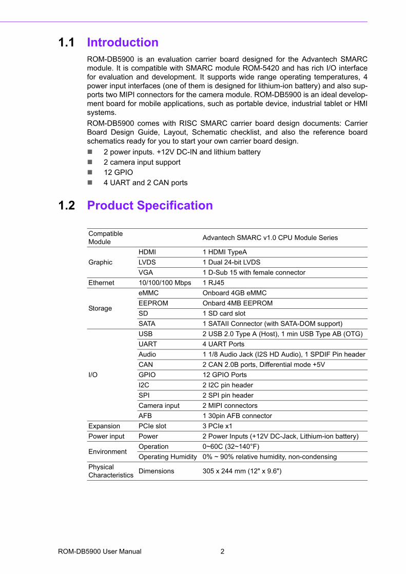
1.1 IntroductionROM-DB5900 is an evaluation carrier board designed for the Advantech SMARCmodule. It is compatible with SMARC module ROM-5420 and has rich I/O interfacefor evaluation and development. It supports wide range operating temperatures, 4power input interfaces (one of them is designed for lithium-ion battery) and also sup-ports two MIPI connectors for the camera module. ROM-DB5900 is an ideal develop-ment board for mobile applications, such as portable device, industrial tablet or HMIsystems.
ROM-DB5900 comes with RISC SMARC carrier board design documents: CarrierBoard Design Guide, Layout, Schematic checklist, and also the reference boardschematics ready for you to start your own carrier board design.
2 power inputs. +12V DC-IN and lithium battery 2 camera input support 12 GPIO 4 UART and 2 CAN ports
1.2 Product Specification
Compatible Module
Advantech SMARC v1.0 CPU Module Series
Graphic
HDMI 1 HDMI TypeA
LVDS 1 Dual 24-bit LVDS
VGA 1 D-Sub 15 with female connector
Ethernet 10/100/100 Mbps 1 RJ45
Storage
eMMC Onboard 4GB eMMC
EEPROM Onbard 4MB EEPROM
SD 1 SD card slot
SATA 1 SATAII Connector (with SATA-DOM support)
I/O
USB 2 USB 2.0 Type A (Host), 1 min USB Type AB (OTG)
UART 4 UART Ports
Audio 1 1/8 Audio Jack (I2S HD Audio), 1 SPDIF Pin header
CAN 2 CAN 2.0B ports, Differential mode +5V
GPIO 12 GPIO Ports
I2C 2 I2C pin header
SPI 2 SPI pin header
Camera input 2 MIPI connectors
AFB 1 30pin AFB connector
Expansion PCIe slot 3 PCIe x1
Power input Power 2 Power Inputs (+12V DC-Jack, Lithium-ion battery)
Environment Operation 0~60C (32~140°F)
Operating Humidity 0% ~ 90% relative humidity, non-condensing
Physical Characteristics
Dimensions 305 x 244 mm (12" x 9.6")
ROM-DB5900 User Manual 2

Chapter 2
2 H/W InstallationThis chapter gives mechanical and connector information on the ROM-DB5900 carrier board.Sections include:
Connector Information
Mechanical Drawing
Hardware Installation
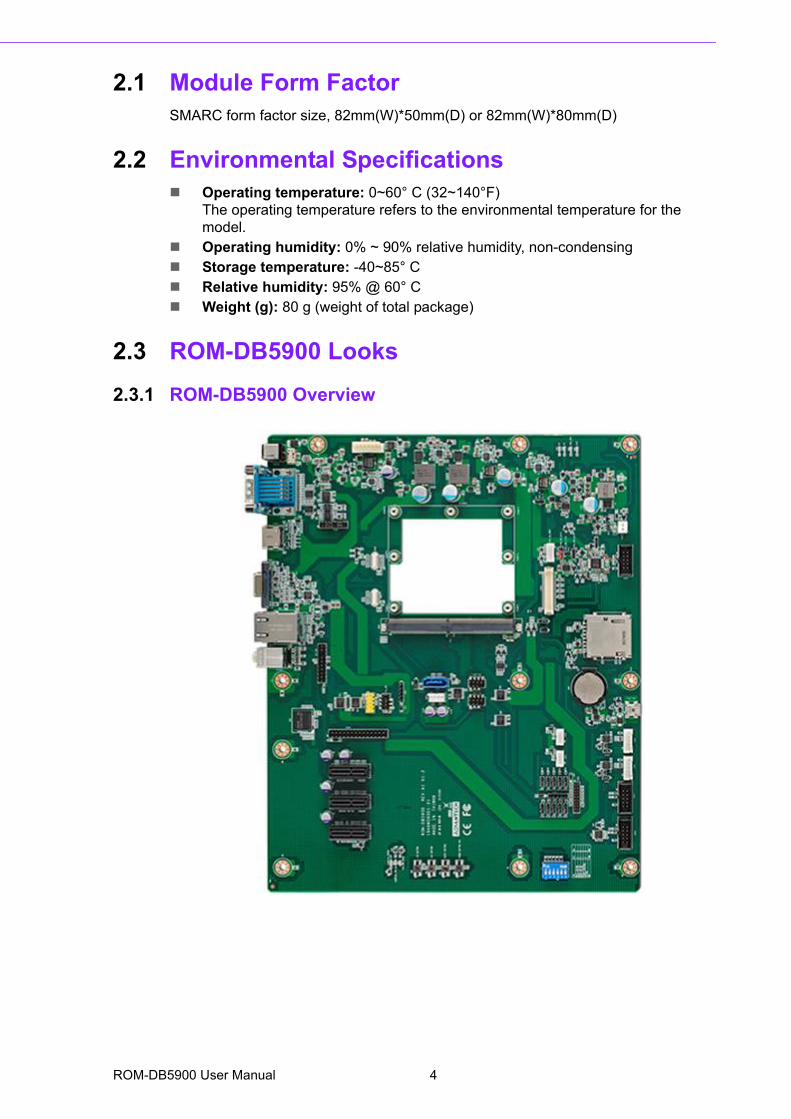
2.1 Module Form FactorSMARC form factor size, 82mm(W)*50mm(D) or 82mm(W)*80mm(D)
2.2 Environmental Specifications Operating temperature: 0~60° C (32~140°F)
The operating temperature refers to the environmental temperature for the model.
Operating humidity: 0% ~ 90% relative humidity, non-condensing Storage temperature: -40~85° C Relative humidity: 95% @ 60° C Weight (g): 80 g (weight of total package)
2.3 ROM-DB5900 Looks
2.3.1 ROM-DB5900 Overview
ROM-DB5900 User Manual 4

Chapter 2
H/W
Installation
2.3.2 I/O Connectors
2.4 Connector, Jumper setting, Switch and LED
2.4.1 Rear I/O panel
Table 2.1: External IO Connector
Position Description
DCIN1 DC Jack A
CN19A UART Port 1 B
CN19B UART Port 2 C
CN42 HDMI Port D
VGA1 VGA Port E
CN5 GbE Ethernet Connector F
CN5 USB Port 1/ 2 G
Audio1 MIC Input/ Audio Output H
Table 2.2: DCIN1 (DC-Jack, +12V power input)
Pin Signal Pin Signal
1 +12V Shield GND
5 ROM-DB5900 User Manual

Table 2.3: CN16A (UART0, 2 wires)
Pin Signal Pin Signal
1 - 2 RX
3 TX 4 -
5 GND 6 -
7 RTS 8 CTS
9 -
Table 2.4: CN16B (UART2, 4 wires)
Pin Signal Pin Signal
1 TXD485- 2 TXD485+
3 RXD485+ 4 RXD485-
5 GND 6 DSR
7 RTS 8 CTS
9 RI
ROM-DB5900 User Manual 6

Chapter 2
H/W
Installation
Table 2.5: VGA1 (VGA)
Pin Signal Pin Signal
1 Red 2 Green
3 Blue 4 -
5 GND 6 GND
7 GND 8 GND
9 +5V 10 GND
11 - 12 DDC_DAT
13 HSYNC 14 VSYNC
15 DDC_CK
Table 2.6: CN42 (HDMI)
Pin Signal Pin Signal
1 TMDS_D2+ 2 GND
3 TMDS_D2- 4 TMDS_D1+
5 GND 6 TMDS_D1-
7 TMDS_D0+ 8 GND
9 TMDS_D0- 10 TMDS_CLK+
11 GND 12 TMDS_CLK-
13 CEC 14 -
15 CTRL_CLK 16 CTRL_DAT
17 GND 18 +5V
19 HPD
7 ROM-DB5900 User Manual
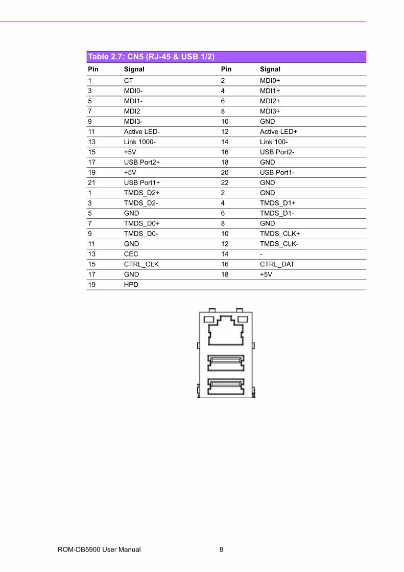
Table 2.7: CN5 (RJ-45 & USB 1/2)
Pin Signal Pin Signal
1 CT 2 MDI0+
3 MDI0- 4 MDI1+
5 MDI1- 6 MDI2+
7 MDI2 8 MDI3+
9 MDI3- 10 GND
11 Active LED- 12 Active LED+
13 Link 1000- 14 Link 100-
15 +5V 16 USB Port2-
17 USB Port2+ 18 GND
19 +5V 20 USB Port1-
21 USB Port1+ 22 GND
1 TMDS_D2+ 2 GND
3 TMDS_D2- 4 TMDS_D1+
5 GND 6 TMDS_D1-
7 TMDS_D0+ 8 GND
9 TMDS_D0- 10 TMDS_CLK+
11 GND 12 TMDS_CLK-
13 CEC 14 -
15 CTRL_CLK 16 CTRL_DAT
17 GND 18 +5V
19 HPD
ROM-DB5900 User Manual 8

Chapter 2
H/W
Installation
2.4.2 Internal I/O
Table 2.8: Audio1 (Audio output)
Pin Signal Pin Signal
1 GND 2 -
3 - 4 -
5 MIC-IN 6 -
7 Audio_L 8 -
9 Audio_R
Table 2.9: Internal IO Connector
Position Description Connector Type
CN1 VDD_IO +3V/1.8V selectionPIN HEADER 3x1P 2.0mm 180D(M) DIP 2000-13 WS
CN2 VMODAPIN HEADER 2*1P 180D(M)SQUARE 2.0mm DIP W/O Pb
CN3 EDP_HPD for LVDSPIN HEADER 3x1P 2.0mm 180D(M) DIP 2000-13 WS
CN5B USB Port1PhoneJack RJ45+USB 22P 90D(F) DIP RU1-196A9WGF
CN5C USB Port2PhoneJack RJ45+USB 22P 90D(F) DIP RU1-196A9WGF
CN6 PCIex1 connector 1PCIEXPRESS 36P 180D(F) DIP 2EG01817-D2D-DF
9 ROM-DB5900 User Manual

CN7 PCIex1 connector 2PCIEXPRESS 36P 180D(F) DIP 2EG01817-D2D-DF
CN8 PCIex1 connector 3PCIEXPRESS 36P 180D(F) DIP 2EG01817-D2D-DF
CN9SATA-DOM Jumper (Power +5V pin7)
PIN HEADER 3x1P 2.0mm 180D(M) DIP 2000-13 WS
CN11 SATA connectorSerial ATA 7P 1.27mm 180D(M) DIP WATM-07DBN4A3B8
CN12 SATA power connectorWAFER 4P 2.5mm 180D(M) DIP 24W1161-04S10-01T
CN13CAN1 bus, 120om terminal resistor
PIN HEADER 2*1P 180D(M)SQUARE 2.0mm DIP W/O Pb
CN14CAN2 bus, 120om terminal resistor
PIN HEADER 2*1P 180D(M)SQUARE 2.0mm DIP W/O Pb
CN15UART2 selection jumper (RS232/422/485)
PIN HEADER 9x2P 2.0mm 180D(M) DIP 21N22050-18S10
CN16A UART0 (RS232)D-SUB Conn. 18P 90D(M) DIP DM10151-H531-4F
CN16B UART2 (RS232/422/485)D-SUB Conn. 18P 90D(M) DIP DM10151-H531-4F
CN17 UART1 (RS232, 2wires)BOX HEADER 5x2P 2.54mm 180D(M) DIP 23N6960-10S10
CN18 UART3 (RS232, 2wires)BOX HEADER 5x2P 2.54mm 180D(M) DIP 23N6960-10S10
CN21 SPDIFPIN HEADER 1X5P 2.54mm 180D 210-91-05GB01
CN22 Camera 1 connector (MIPI)B/B CONN. 2x15P 0.5mm 180D(M) SMD DF12 (3.0)-30D
CN23 Camera 2 connector (MIPI)B/B CONN. 2x15P 0.5mm 180D(M) SMD DF12 (3.0)-30D
CN24GPIO0 (Reserved for multi-function)
PIN HEADER 3x1P 2.0mm 180D(M) DIP 2000-13 WS
CN25GPIO9 (Reserved for multi-function)
PIN HEADER 3x1P 2.0mm 180D(M) DIP 2000-13 WS
CN26GPIO1 (Reserved for multi-function)
PIN HEADER 3x1P 2.0mm 180D(M) DIP 2000-13 WS
CN27GPIO2 (Reserved for multi-function)
PIN HEADER 3x1P 2.0mm 180D(M) DIP 2000-13 WS
CN28GPIO3 (Reserved for multi-function)
PIN HEADER 3x1P 2.0mm 180D(M) DIP 2000-13 WS
CN29 Reserved for CANPIN HEADER 1X5P 2.54mm 180D 210-91-05GB01
CN30GPIO4 (Reserved for multi-function)
PIN HEADER 3x1P 2.0mm 180D(M) DIP 2000-13 WS
CN31GPIO5 (Reserved for multi-function)
PIN HEADER 3x1P 2.0mm 180D(M) DIP 2000-13 WS
CN32GPIO6 (Reserved for multi-function)
PIN HEADER 3x1P 2.0mm 180D(M) DIP 2000-13 WS
CN33 GPIO connectorPIN HEADER 10x2P 2.0mm 180D(M) DIP 21N22050
CN34 GPIO8PIN HEADER 3x1P 2.0mm 180D(M) DIP 2000-13 WS
CN35 GPIO7PIN HEADER 3x1P 2.0mm 180D(M) DIP 2000-13 WS
ROM-DB5900 User Manual 10
Chapter 2
H/W
Installation
CN37 External WDT out PIN HEADER 2*1P 180D(M)SQUARE 2.0mm DIP W/O Pb
CN38 System Fan Wafer 2.54mm 3P 180D(M) DIP 22-27-2031
CN39 AFBPIN HEADER 2x15P 2.54mm 180D(M) 21N22564-30S10B-
CN40 Reserved for EC programming BOX HEADER 5x2P 2.54mm 180D(M) DIP 23N6960-10S10
CN41 MXM 3.0 connector
CN42 HDMI connectorHDMI Conn. 19P 0.5mm 90D(F) SMD QJ51191-LFB4-7F
I2C1 I2C pin headerWAFER BOX 2.0mm 4P 180D(M) W/LOCK A2001WV2-4P
I2C2 I2C pin headerWAFER BOX 2.0mm 4P 180D(M) W/LOCK A2001WV2-4P
I2C_CN1 I2S1PIN HEADER 2x4P 2.54mm 180D(M) SMD 21N22564
I2C_CN2 I2S2PIN HEADER 2x5P 2.54mm 180D(M) DIP 21N22564-10S1
I2C_CN3 Audio codec connectorPIN HEADER 2x10P 2.54mm 180D(M) DIP 21N22564
SPI_CN1 SPI connector 1PIN HEADER 2x4P 2.54mm 180D(M) SMD 21N22564
SPI_CN2 SPI connector 0PIN HEADER 2x4P 2.54mm 180D(M) SMD 21N22564
SW1 Boot Selection DIP SW EDG106S DIP 6P Radial SPST
SW2 Reset button TACT SW STS-091 SMD 4P H=3.8mm
SW3 Sleep button TACT SW STS-091 SMD 4P H=3.8mm
SW6 Power on (CPU module) TACT SW STS-091 SMD 4P H=3.8mm
SW7 LID Switch SW ESD101E65Z SMD 2P 2.5x6.6x3.1mm
LVDS1 LVDS 24bitB/B Conn. 40P 1.25mm 90D SMD DF13-40DP-1.25V(91)
LVDS_BK_PWR1
LVDS backlight powerWAFER BOX 2.0mm 5P 180D(M) DIP WO/Pb JIH VEI
LVDS_BK_SLT1
LVDS backlight selection (+12V/5V)
PIN HEADER 3x1P 2.54mm 180D(M) DIP 205-1x3GS
LVDS_VDD_SLT1
LVDS VDD power selection (+3.3V/+5V)
PIN HEADER 3x1P 2.0mm 180D(M) DIP 2000-13 WS
LVDS_VDD_SLT2
LVDS VDD power selection2(+12V)
PIN HEADER 2*1P 180D(M)SQUARE 2.0mm DIP W/O Pb
USB_OTG1 USB OTG MINI USB 5P 180D(F) SMD UH51543-CS7-7F
CAN1 CAN0 pin headerWAFER BOX 5P 2.5mm 180D(M) DIP A2501WV2-5P
CAN2 CAN1 pin headerWAFER BOX 5P 2.5mm 180D(M) DIP A2501WV2-5P
BAT1 Lithium-ion Battery power inputWAFER 8P 2.54mm 180D(M) DIP A2543WV2-8P
BH1 CR-2032 connectorBATTERY HOLDER 24.9*23.4*8.9 CR2032 BH800.4GG
SD1 SD socketSD CONN 9P 90D(F) SMD DM1AA-SF-PEJ(82)
DCIN1 DC Power in (+12V)DC POWER JACK 2.5mm 90D(M) DIP 2DC-G213B200
11 ROM-DB5900 User Manual
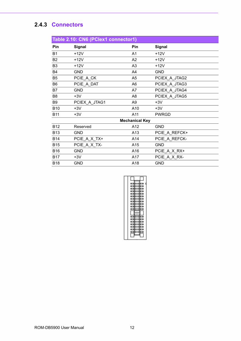
2.4.3 Connectors
Table 2.10: CN6 (PCIex1 connector1)
Pin Signal Pin Signal
B1 +12V A1 +12V
B2 +12V A2 +12V
B3 +12V A3 +12V
B4 GND A4 GND
B5 PCIE_A_CK A5 PCIEX_A_JTAG2
B6 PCIE_A_DAT A6 PCIEX_A_JTAG3
B7 GND A7 PCIEX_A_JTAG4
B8 +3V A8 PCIEX_A_JTAG5
B9 PCIEX_A_JTAG1 A9 +3V
B10 +3V A10 +3V
B11 +3V A11 PWRGD
Mechanical Key
B12 Reserved A12 GND
B13 GND A13 PCIE_A_REFCK+
B14 PCIE_A_X_TX+ A14 PCIE_A_REFCK-
B15 PCIE_A_X_TX- A15 GND
B16 GND A16 PCIE_A_X_RX+
B17 +3V A17 PCIE_A_X_RX-
B18 GND A18 GND
ROM-DB5900 User Manual 12

Chapter 2
H/W
Installation
Table 2.11: CN7 (PCIex1 connector2)
Pin Signal Pin Signal
B1 +12V A1 +12V
B2 +12V A2 +12V
B3 +12V A3 +12V
B4 GND A4 GND
B5 PCIE_B_CK A5 PCIEX_B_JTAG2
B6 PCIE_B_DAT A6 PCIEX_B_JTAG3
B7 GND A7 PCIEX_B_JTAG4
B8 +3V A8 PCIEX_B_JTAG5
B9 PCIEX_B_JTAG1 A9 +3V
B10 +3V A10 +3V
B11 +3V A11 PWRGD
Mechanical Key
B12 Reserved A12 GND
B13 GND A13 PCIE_B_REFCK+
B14 PCIE_B_X_TX+ A14 PCIE_B_REFCK-
B15 PCIE_B_X_TX- A15 GND
B16 GND A16 PCIE_B_X_RX+
B17 +3V A17 PCIE_B_X_RX-
B18 GND A18 GND
1 GND 2 -
3 - 4 -
5 MIC-IN 6 -
7 Audio_L 8 -
9 Audio_R
13 ROM-DB5900 User Manual

Table 2.12: CN8 (PCIex1 connector3)
Pin Signal Pin Signal
B1 +12V A1 +12V
B2 +12V A2 +12V
B3 +12V A3 +12V
B4 GND A4 GND
B5 PCIE_C_CK A5 PCIEX_C_JTAG2
B6 PCIE_C_DAT A6 PCIEX_C_JTAG3
B7 GND A7 PCIEX_C_JTAG4
B8 +3V A8 PCIEX_C_JTAG5
B9 PCIEX_C_JTAG1 A9 +3V
B10 +3V A10 +3V
B11 +3V A11 PWRGD
Mechanical Key
B12 Reserved A12 GND
B13 GND A13 PCIE_C_REFCK+
B14 PCIE_C_X_TX+ A14 PCIE_C_REFCK-
B15 PCIE_C_X_TX- A15 GND
B16 GND A16 PCIE_C_X_RX+
B17 +3V A17 PCIE_C_X_RX-
B18 GND A18 GND
1 GND 2 -
3 - 4 -
5 MIC-IN 6 -
7 Audio_L 8 -
9 Audio_R
ROM-DB5900 User Manual 14

Chapter 2
H/W
Installation
Table 2.13: CN11 (SATA connector)
Pin Signal Pin Signal
1 GND 2 SATA_TX+
3 SATA_TX- 4 GND
5 SATA_RX- 6 SATA_RX+
7 SATA DOM PIN7
Table 2.14: CN12 (SATA Power connector)1 +5V 2 GND
3 GND 4 GND
5 +12V - -
15 ROM-DB5900 User Manual

Table 2.15: CN41 (CN41A, MXM 3.0 connector)
Pin Signal Pin Signal
P1 PCAM_PXL_CK1 S1 PCAM_VSYNC
P2 GND S2 PCAM_HSYNC
P3 CSI1_CK+ S3 GND
P4 CSI1_CK- S4 PCAM_PXL_CK0
P5 - S5 I2C_CAM_CK
P6 PCAM_MCK S6 CAM_MCK
P7 CSI1_D0+ S7 I2C_CAM_DAT
P8 CSI1_D0- S8 CSI0_CK+
P9 GND S9 CSI0_CK-
P10 CSI1_D1+ S10 GND
P11 CSI1_D1- S11 CSI0_D0+
P12 GND S12 CSI0_D0-
P13 CSI1_D2+ S13 GND
P14 CSI1_D2- S14 CSI0_D1+
P15 GND S15 CSI0_D1-
P16 CSI1_D3+ S16 GND
P17 CSI1_D3- S17 AFB0_OUT
P18 GND S18 AFB1_OUT
P19 GBE_MDI3- S19 AFB2_OUT
P20 GBE_MDI3+ S20 AFB3_IN
P21 GBE_LINK100# S21 AFB4_IN
P22 GBE_LINK1000# S22 AFB5_IN
P23 GBE_MDI2- S23 AFB6_PTIO
P24 GBE_MDI2+ S24 AFB7_PTIO
P25 GBE_LINK_ACT# S25 GND
P26 GBE_MDI1- S26 SDMMC_D0
P27 GBE_MDI1+ S27 SDMMC_D1
P28 GBE_CTREF S28 SDMMC_D2
P29 GBE_MDI0- S29 SDMMC_D3
P30 GBE_MDI0+ S30 SDMMC_D4
P31 SPI0_CS1# S31 SDMMC_D5
P32 GND S32 SDMMC_D6
P33 SDIO_WP S33 SDMMC_D7
P34 SDIO_CMD S34 GND
P35 SDIO_CD# S35 SDMMC_CK
P36 SDIO_CK S36 SDMMC_CMD
P37 SDIO_PWR_EN S37 SDMMC_RST#
P38 GND S38 AUDIO_MCK
P39 SDIO_D0 S39 I2S0_LRCK
P40 SDIO_D1 S40 I2S0_SDOUT
P41 SDIO_D2 S41 I2S0_SDIN
P42 SDIO_D3 S42 I2S0_CK
P43 SPI0_CS0# S43 I2S1_LRCK
P44 SPI0_CK S44 I2S1_SDOUT
P45 SPI0_DIN S45 I2S1_SDIN
ROM-DB5900 User Manual 16

Chapter 2
H/W
Installation
P46 SPI0_DO S46 I2S1_CK
P47 GND S47 GND
P48 SATA_TX+ S48 I2C_GP_CK
P49 SATA_TX- S49 I2C_GP_DAT
P50 GND S50 I2S2_LRCK
P51 SATA_RX+ S51 I2S2_SDOUT
P52 SATA_RX- S52 I2S2_SDIN
P53 GND S53 I2S2_CK
P54 SPI1_CS0# S54 SATA_ACT#
P55 SPI1_CS1# S55 AFB8_PTIO
P56 SPI1_CK S56 AFB9_PTIO
P57 SPI1_DIN S57 PCAM_ON_CSI0#
P58 SPI1_DO S58 PCAM_ON_CSI1#
P59 GND S59 SPDIF_OUT
P60 USB0+ S60 SPDIF_IN
P61 USB0- S61 GND
P62 USB0_EN_OC# S62 AFB_DIFF0+
P63 USB0_VBUS_DET S63 AFB_DIFF0-
P64 USB0_OTG_ID S64 GND
P65 USB1+ S65 AFB_DIFF1+
P66 USB1- S66 AFB_DIFF1-
P67 USB1_EN_OC# S67 GND
P68 GND S68 AFB_DIFF2+
P69 USB2+ S69 AFB_DIFF2-
P70 USB2- S70 GND
P71 USB2_EN_OC# S71 AFB_DIFF3+
P72 PCIE_C_PRSNT# S72 AFB_DIFF3-
P73 PCIE_B_PRSNT# S73 GND
P74 PCIE_B_PRSNT# S74 AFB_DIFF4+
P75 PCIE_A_RST# S75 AFB_DIFF4-
P76 PCIE_C_CKREQ# S76 PCIE_B_RST#
P77 PCIE_B_CKREQ# S77 PCIE_C_RST#
P78 PCIE_A_CKREQ# S78 PCIE_C_RX+
P79 GND S79 PCIE_C_RX-
P80 PCIE_C_REFCK+ S80 GND
P81 PCIE_C_REFCK- S81 PCIE_C_TX+
P82 GND S82 PCIE_C_TX-
P83 PCIE_A_REFCK+ S83 GND
P84 PCIE_A_REFCK- S84 PCIE_B_REFCK+
P85 GND S85 PCIE_B_REFCK-
P86 PCIE_A_RX+ S86 GND
P87 PCIE_A_RX- S87 PCIE_B_RX+
P88 GND S88 PCIE_B_RX-
P89 PCIE_A_TX+ S89 GND
P90 PCIE_A_TX- S90 PCIE_B_TX+
P91 GND S91 PCIE_B_TX-
P92 HDMI_D2+ S92 GND
Table 2.15: CN41 (CN41A, MXM 3.0 connector)
17 ROM-DB5900 User Manual
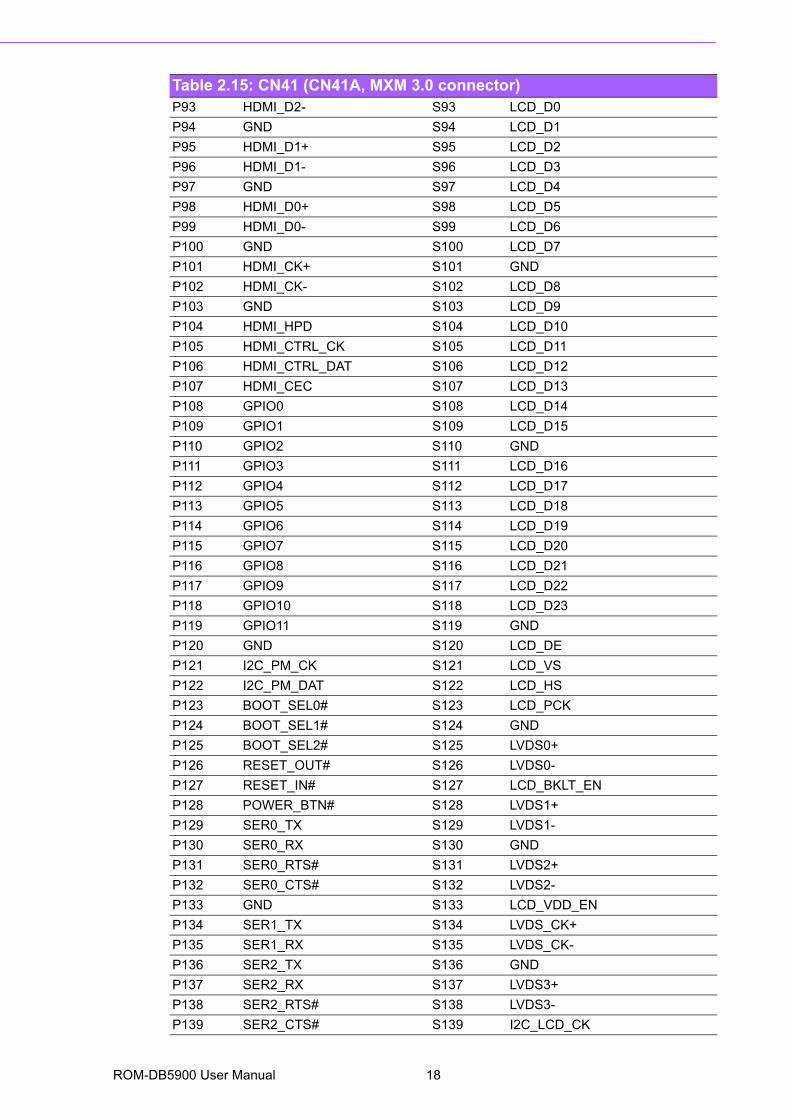
P93 HDMI_D2- S93 LCD_D0
P94 GND S94 LCD_D1
P95 HDMI_D1+ S95 LCD_D2
P96 HDMI_D1- S96 LCD_D3
P97 GND S97 LCD_D4
P98 HDMI_D0+ S98 LCD_D5
P99 HDMI_D0- S99 LCD_D6
P100 GND S100 LCD_D7
P101 HDMI_CK+ S101 GND
P102 HDMI_CK- S102 LCD_D8
P103 GND S103 LCD_D9
P104 HDMI_HPD S104 LCD_D10
P105 HDMI_CTRL_CK S105 LCD_D11
P106 HDMI_CTRL_DAT S106 LCD_D12
P107 HDMI_CEC S107 LCD_D13
P108 GPIO0 S108 LCD_D14
P109 GPIO1 S109 LCD_D15
P110 GPIO2 S110 GND
P111 GPIO3 S111 LCD_D16
P112 GPIO4 S112 LCD_D17
P113 GPIO5 S113 LCD_D18
P114 GPIO6 S114 LCD_D19
P115 GPIO7 S115 LCD_D20
P116 GPIO8 S116 LCD_D21
P117 GPIO9 S117 LCD_D22
P118 GPIO10 S118 LCD_D23
P119 GPIO11 S119 GND
P120 GND S120 LCD_DE
P121 I2C_PM_CK S121 LCD_VS
P122 I2C_PM_DAT S122 LCD_HS
P123 BOOT_SEL0# S123 LCD_PCK
P124 BOOT_SEL1# S124 GND
P125 BOOT_SEL2# S125 LVDS0+
P126 RESET_OUT# S126 LVDS0-
P127 RESET_IN# S127 LCD_BKLT_EN
P128 POWER_BTN# S128 LVDS1+
P129 SER0_TX S129 LVDS1-
P130 SER0_RX S130 GND
P131 SER0_RTS# S131 LVDS2+
P132 SER0_CTS# S132 LVDS2-
P133 GND S133 LCD_VDD_EN
P134 SER1_TX S134 LVDS_CK+
P135 SER1_RX S135 LVDS_CK-
P136 SER2_TX S136 GND
P137 SER2_RX S137 LVDS3+
P138 SER2_RTS# S138 LVDS3-
P139 SER2_CTS# S139 I2C_LCD_CK
Table 2.15: CN41 (CN41A, MXM 3.0 connector)
ROM-DB5900 User Manual 18
Chapter 2
H/W
Installation
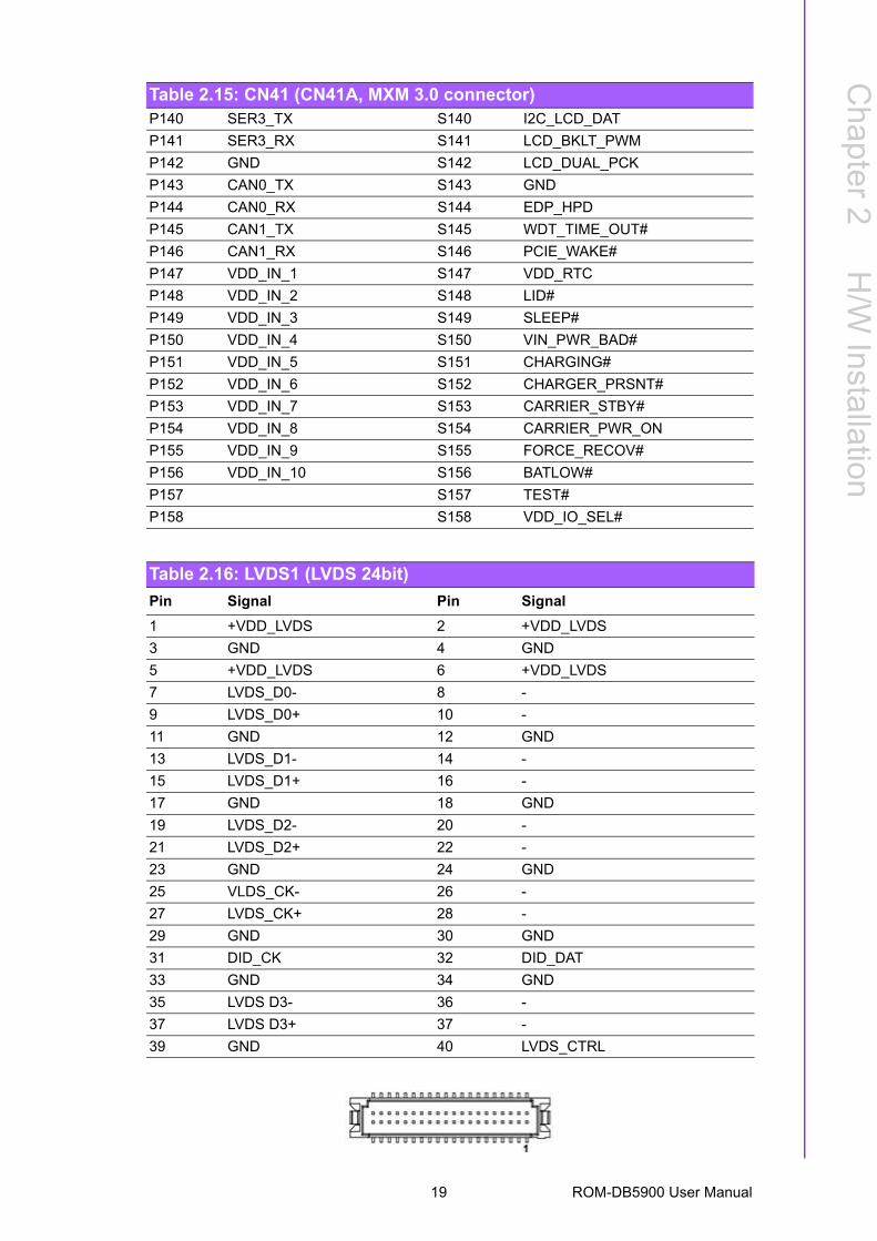
P140 SER3_TX S140 I2C_LCD_DAT
P141 SER3_RX S141 LCD_BKLT_PWM
P142 GND S142 LCD_DUAL_PCK
P143 CAN0_TX S143 GND
P144 CAN0_RX S144 EDP_HPD
P145 CAN1_TX S145 WDT_TIME_OUT#
P146 CAN1_RX S146 PCIE_WAKE#
P147 VDD_IN_1 S147 VDD_RTC
P148 VDD_IN_2 S148 LID#
P149 VDD_IN_3 S149 SLEEP#
P150 VDD_IN_4 S150 VIN_PWR_BAD#
P151 VDD_IN_5 S151 CHARGING#
P152 VDD_IN_6 S152 CHARGER_PRSNT#
P153 VDD_IN_7 S153 CARRIER_STBY#
P154 VDD_IN_8 S154 CARRIER_PWR_ON
P155 VDD_IN_9 S155 FORCE_RECOV#
P156 VDD_IN_10 S156 BATLOW#
P157 S157 TEST#
P158 S158 VDD_IO_SEL#
Table 2.16: LVDS1 (LVDS 24bit)
Pin Signal Pin Signal
1 +VDD_LVDS 2 +VDD_LVDS
3 GND 4 GND
5 +VDD_LVDS 6 +VDD_LVDS
7 LVDS_D0- 8 -
9 LVDS_D0+ 10 -
11 GND 12 GND
13 LVDS_D1- 14 -
15 LVDS_D1+ 16 -
17 GND 18 GND
19 LVDS_D2- 20 -
21 LVDS_D2+ 22 -
23 GND 24 GND
25 VLDS_CK- 26 -
27 LVDS_CK+ 28 -
29 GND 30 GND
31 DID_CK 32 DID_DAT
33 GND 34 GND
35 LVDS D3- 36 -
37 LVDS D3+ 37 -
39 GND 40 LVDS_CTRL
Table 2.15: CN41 (CN41A, MXM 3.0 connector)
19 ROM-DB5900 User Manual
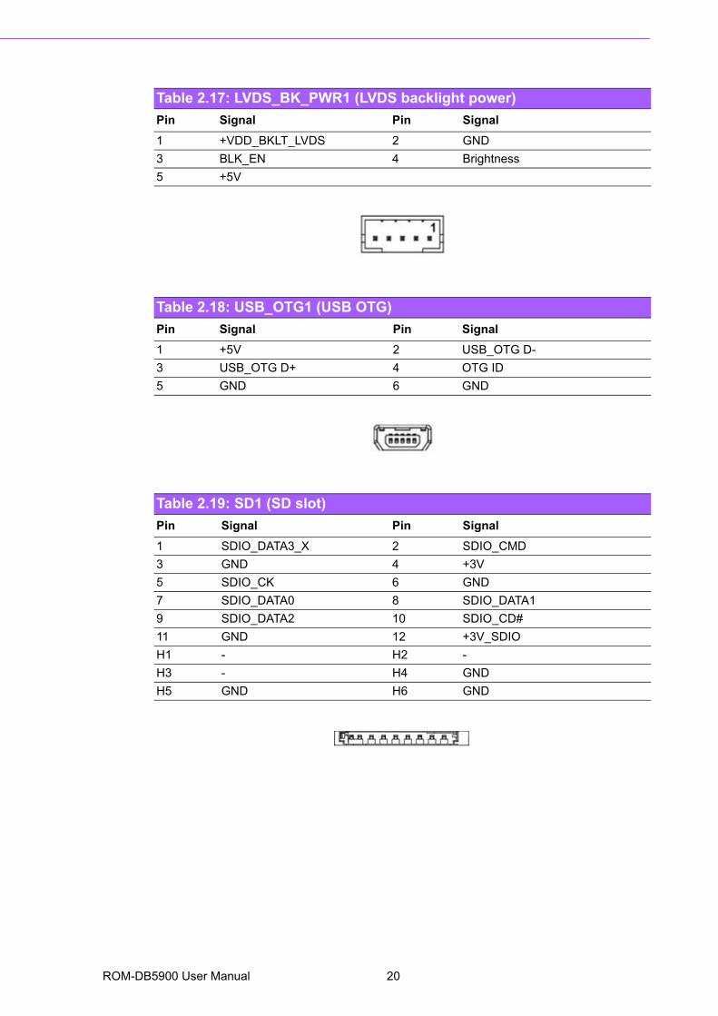
Table 2.17: LVDS_BK_PWR1 (LVDS backlight power)
Pin Signal Pin Signal
1 +VDD_BKLT_LVDS 2 GND
3 BLK_EN 4 Brightness
5 +5V
Table 2.18: USB_OTG1 (USB OTG)
Pin Signal Pin Signal
1 +5V 2 USB_OTG D-
3 USB_OTG D+ 4 OTG ID
5 GND 6 GND
Table 2.19: SD1 (SD slot)
Pin Signal Pin Signal
1 SDIO_DATA3_X 2 SDIO_CMD
3 GND 4 +3V
5 SDIO_CK 6 GND
7 SDIO_DATA0 8 SDIO_DATA1
9 SDIO_DATA2 10 SDIO_CD#
11 GND 12 +3V_SDIO
H1 - H2 -
H3 - H4 GND
H5 GND H6 GND
ROM-DB5900 User Manual 20

Chapter 2
H/W
Installation
2.4.4 Jumpers
Table 2.20: BAT1 (Lithium-ion Battery power input)
Pin Signal Pin Signal
1 GND 2 GND
3 BAT_THER 4 BAT_ID_CN
5 I2C_DAT_BAT 6 I2C_CK_BAT
7 +VBATT 8 +VBATT
Table 2.21: BH1 (CR-2032)
Pin Signal Pin Signal
1 BAT_RTC 2 GND
Table 2.22: CN1 (VDD_IO+3V/1.8V selection)
Pin Signal Pin Signal
1 +3V 2 +VDD_IO
3 +1.8V
Table 2.23: CN2 (WMODA)
Pin Signal Pin Signal
1 +VMODA 2 GND
21 ROM-DB5900 User Manual

Table 2.24: CN3 (EDP_HPD for LVDS)
Pin Signal Pin Signal
1 GND 2 EDP_HDP_A
3 EDP_HPD
Table 2.25: CN9 (SATA-DOM Jumper, default 2-3)
Pin Signal Pin Signal
1 +5V 2 SATA-DOM Pin7
3 GND - -
Table 2.26: CN13 (CAN0 bus, 120OM terminal resistor)
Jumper Mode Jumper Mode
1-2 120 OM (Default) - Without 120 OM
Table 2.27: CN14 (CAN1 bus, 120OM terminal resistor)
Jumper Mode Jumper Mode
1-2 120 OM (Default) - Without 120 OM
ROM-DB5900 User Manual 22

Chapter 2
H/W
Installation
Jumper Mode Jumper Mode
1-2 120 OM (Default) - Without 120 OM
Table 2.28: CN18 (UART2 function selection)
Pin Signal Pin Signal
1 SER2_RX 2 RXD485_A
3 SER2_RX 4 RXD422_A
5 SER2_RX 6 RXD232_A
7 - 8 COM2_RXD
9 NDCD#TXD485- 10 NRXD2TXD485+
11 TXD485-_A 12 TXD485+_A
13 COM2_TXD 14 -
15 NTXD2_RXD485+ 16 NDTR#2_RXD485-
17 RSD485+_A 18 RSD485-_A
Table 2.29: CN17 (UART1, 2wires)
Pin Signal Pin Signal
1 - 2 -
3 COM1_RX 4 -
5 COM1_TX 6 -
7 - 8 -
9 GND 10 -
23 ROM-DB5900 User Manual
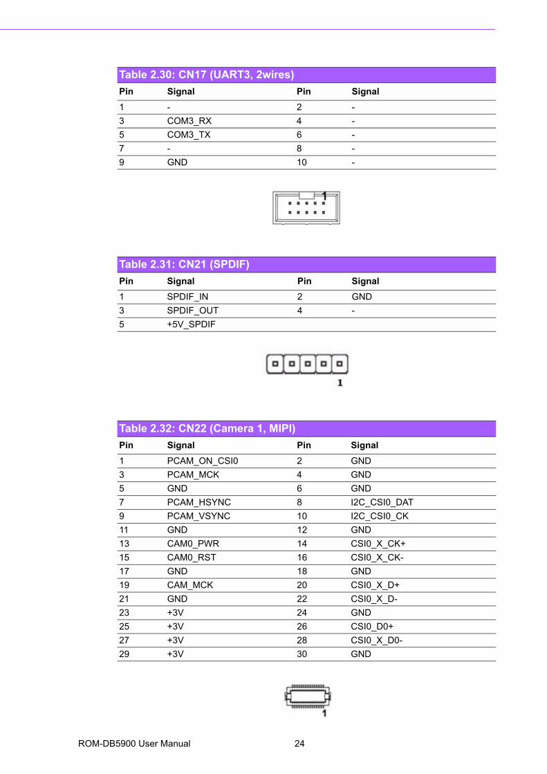
Table 2.30: CN17 (UART3, 2wires)
Pin Signal Pin Signal
1 - 2 -
3 COM3_RX 4 -
5 COM3_TX 6 -
7 - 8 -
9 GND 10 -
Table 2.31: CN21 (SPDIF)
Pin Signal Pin Signal
1 SPDIF_IN 2 GND
3 SPDIF_OUT 4 -
5 +5V_SPDIF
Table 2.32: CN22 (Camera 1, MIPI)
Pin Signal Pin Signal
1 PCAM_ON_CSI0 2 GND
3 PCAM_MCK 4 GND
5 GND 6 GND
7 PCAM_HSYNC 8 I2C_CSI0_DAT
9 PCAM_VSYNC 10 I2C_CSI0_CK
11 GND 12 GND
13 CAM0_PWR 14 CSI0_X_CK+
15 CAM0_RST 16 CSI0_X_CK-
17 GND 18 GND
19 CAM_MCK 20 CSI0_X_D+
21 GND 22 CSI0_X_D-
23 +3V 24 GND
25 +3V 26 CSI0_D0+
27 +3V 28 CSI0_X_D0-
29 +3V 30 GND
ROM-DB5900 User Manual 24
Chapter 2
H/W
Installation
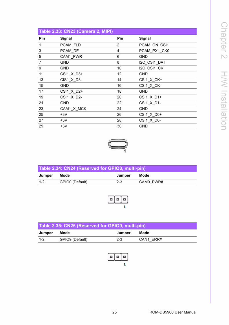
Table 2.33: CN23 (Camera 2, MIPI)
Pin Signal Pin Signal
1 PCAM_FLD 2 PCAM_ON_CSI1
3 PCAM_DE 4 PCAM_PXL_CK0
5 CAM1_PWR 6 GND
7 GND 8 I2C_CSI1_DAT
9 GND 10 I2C_CSI1_CK
11 CSI1_X_D3+ 12 GND
13 CIS1_X_D3- 14 CSI1_X_CK+
15 GND 16 CSI1_X_CK-
17 CSI1_X_D2+ 18 GND
19 CSI1_X_D2- 20 CSI1_X_D1+
21 GND 22 CSI1_X_D1-
23 CAM1_X_MCK 24 GND
25 +3V 26 CSI1_X_D0+
27 +3V 28 CSI1_X_D0-
29 +3V 30 GND
Table 2.34: CN24 (Reserved for GPIO0, multi-pin)
Jumper Mode Jumper Mode
1-2 GPIO0 (Default) 2-3 CAM0_PWR#
Table 2.35: CN25 (Reserved for GPIO9, multi-pin)
Jumper Mode Jumper Mode
1-2 GPIO9 (Default) 2-3 CAN1_ERR#
25 ROM-DB5900 User Manual

Table 2.36: CN26 (Reserved for GPIO1, multi-pin)
Jumper Mode Jumper Mode
1-2 GPIO1 (Default) 2-3 CAM1_PWR
Table 2.37: CN27 (Reserved for GPIO2, multi-pin)
Jumper Mode Jumper Mode
1-2 GPIO2 (Default) 2-3 CAM0_RST#
Table 2.38: CN28 (Reserved for GPIO3, multi-pin)
Jumper Mode Jumper Mode
1-2 GPIO3 (Default) 2-3 CAM1_RST#
Table 2.39: CN29 (Reserved for CAN, multi-pin)
Pin Signal Pin Signal
1 +3V 2 CAN0_ERR#
3 CAN1_ERR# 4 -
5 GND
ROM-DB5900 User Manual 26
Chapter 2
H/W
Installation
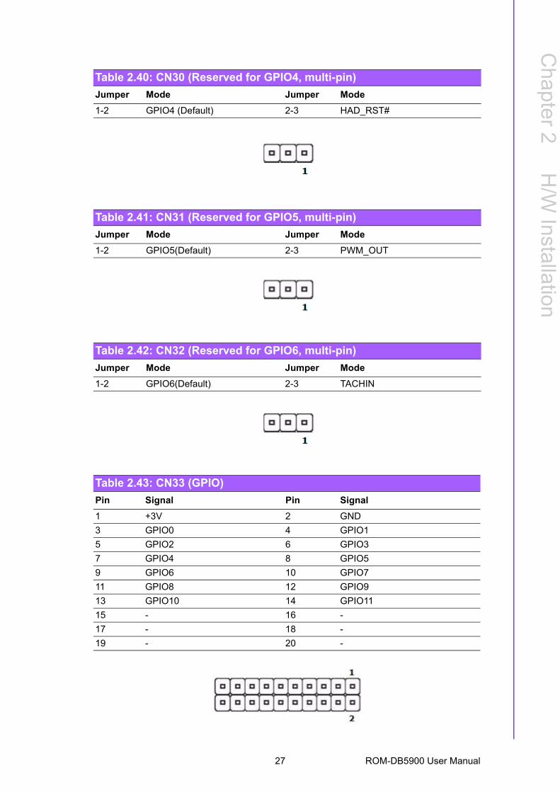
Table 2.40: CN30 (Reserved for GPIO4, multi-pin)
Jumper Mode Jumper Mode
1-2 GPIO4 (Default) 2-3 HAD_RST#
Table 2.41: CN31 (Reserved for GPIO5, multi-pin)
Jumper Mode Jumper Mode
1-2 GPIO5(Default) 2-3 PWM_OUT
Table 2.42: CN32 (Reserved for GPIO6, multi-pin)
Jumper Mode Jumper Mode
1-2 GPIO6(Default) 2-3 TACHIN
Table 2.43: CN33 (GPIO)
Pin Signal Pin Signal
1 +3V 2 GND
3 GPIO0 4 GPIO1
5 GPIO2 6 GPIO3
7 GPIO4 8 GPIO5
9 GPIO6 10 GPIO7
11 GPIO8 12 GPIO9
13 GPIO10 14 GPIO11
15 - 16 -
17 - 18 -
19 - 20 -
27 ROM-DB5900 User Manual

Table 2.44: CN34 (Reserved for GPIO8, multi-pin)
Jumper Mode Jumper Mode
1-2 GPIO8(Default) 2-3 CAN0_ERR#
Table 2.45: CN35 (Reserved for GPIO7, multi-pin)
Jumper Mode Jumper Mode
1-2 GPIO7(Default) 2-3 PCAM_FLD
Table 2.46: CN37 (External WDT)
Pin Signal Pin Signal
1 WDT_Time_Out# 2 GND
Table 2.47: CN38 (System FAN)
Pin Signal Pin Signal
1 GND 2 +12V
3 +5V
ROM-DB5900 User Manual 28

Chapter 2
H/W
Installation
Table 2.48: CN39 (AFB, Reserved)
Pin Signal Pin Signal
1 +3V 2 +3V
3 AFB0_OUT 4 AFB_DIFF0+
5 AFB1_OUT 6 AFB_DIFF0-
7 AFB2_OUT 8 GND
9 GND 10 AFB_DIFF1+
11 AFB3_IN 12 AFB_DIFF1-
13 AFB4_IN 14 GND
15 AFB5_IN 16 AFB_DIFF2+
17 GND 18 AFB_DIFF2-
19 AFB6_PTIO 20 GND
21 AFB7_PTIO 22 AFB_DIFF3+
23 GND 24 AFB_DIFF3-
25 AFB8_PTIO 26 GND
27 AFB9_PTIO 28 AFB_DIFF4+
29 GND 30 AFB_DIFF4-
Table 2.49: CN40 (Reserved for EC, programming pin)
Pin Signal Pin Signal
1 - 2 -
3 EC_RXD 4 -
5 EC_TXD 6 -
7 - 8 -
9 GND 10 -
29 ROM-DB5900 User Manual

Table 2.50: I2C_CN1 (I2S1)
Pin Signal Pin Signal
1 Audio_VDDA1 2 GND
3 I2S1_SDOUT_C 3 I2S1_SDIN_C
5 I2S1_CK_C 6 I2S1_LRCK_C
7 - 8 AUDIO_MCK_C
Table 2.51: I2C_CN2 (I2S2)
Pin Signal Pin Signal
1 Audio_VDDA2 2 GND
3 I2S2_SDOUT_C 3 I2S2_SDIN_C
5 I2S2_CK_C 6 I2S2_LRCK_C
7 - 8 AUDIO_MCK_C
Table 2.52: I2C_CN3 (I2S0, audio codec)
Pin Signal Pin Signal
1 Audio_VDDA 2 GND
3 Audio_VDDA 4 I2S0_SDIN_C
5 I2S0_SDOUT_C 6 I2S0_LRCK_C
7 I2S0_CK_C 8 AUDIO_MCK_C
9 - 10 GND
11 Audio_I2C_CK 12 MIC_BIAS
13 Audio_I2C_DAT 14 GND
15 - 16 HP_R
17 MIC_IN 18 GND
19 GND 20 HP_L
ROM-DB5900 User Manual 30

Chapter 2
H/W
Installation
* +VDD_BKLT_LVDS, pin1
Table 2.53: SPI_CN1 (SPI1)
Pin Signal Pin Signal
1 +3V 2 GND
3 SPI1_CS0# 3 SPI1_CK
5 SPI1_DO_C 6 SPI1_DIN_C
7 - 8 SPI1_CS1#_C
Table 2.54: SPI_CN2 (SPI0)
Pin Signal Pin Signal
1 +3V 2 GND
3 SPI0_CS0# 3 SPI0_CK
5 SPI0_DO_C 6 SPI0_DIN_C
7 - 8 SPI0_CS1#_C
Table 2.55: LVDS_BK_SLT1 (LVDS backlight selection)
Jumper Mode Jumper Mode
1-2 +5V (Default) 2-3 +12V
31 ROM-DB5900 User Manual

Table 2.56: LVDS_VDD_SLT1 (LVDS VDD Power selection)
Jumper Mode Jumper Mode
1-2 +12V (Default) 2-3 +5V
Table 2.57: LVDS_VDD_SLT2 (LVDS VDD Power selection2)
Jumper Mode Jumper Mode
1-2 +12V (Default)
Table 2.58: CAN1 (CAN0)
Pin Signal Pin Signal
1 - 2 -
3 CAN0_D- 4 CAN0_D+
5 GND
Table 2.59: CAN2 (CAN1)
Pin Signal Pin Signal
1 - 2 -
3 CAN1_D- 4 CAN1_D+
5 GND
ROM-DB5900 User Manual 32
Chapter 2
H/W
Installation
2.4.5 Switches and buttons
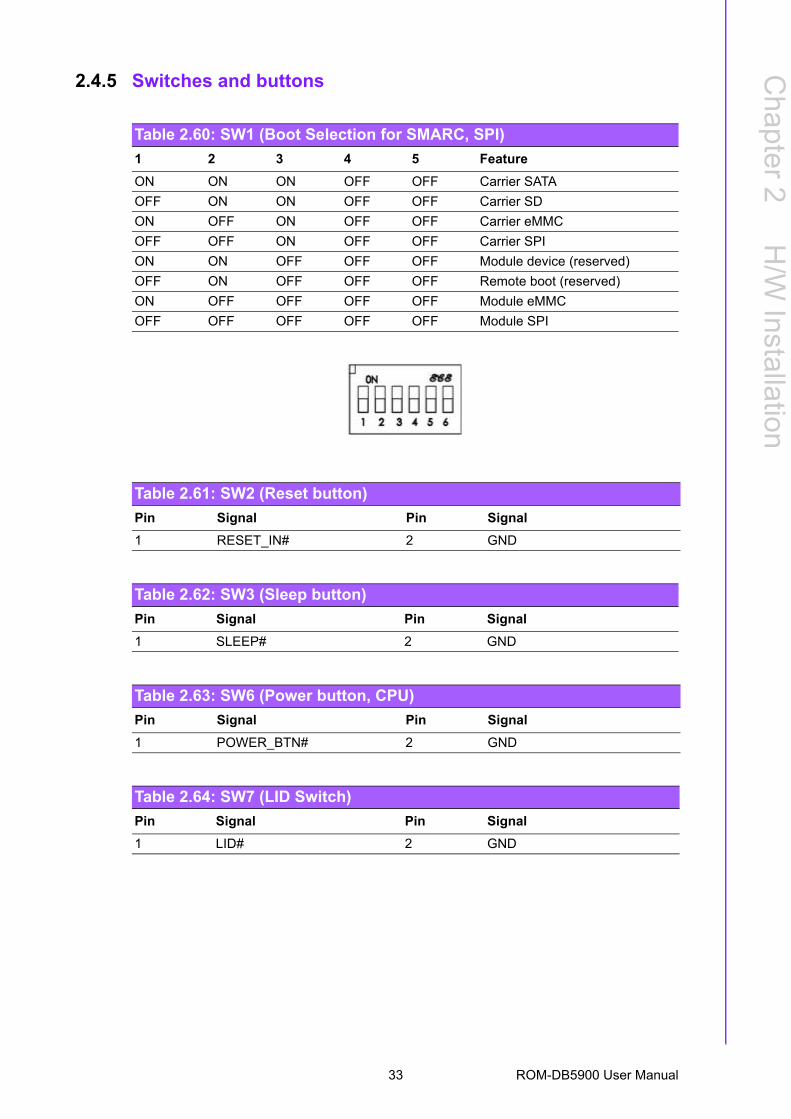
Table 2.60: SW1 (Boot Selection for SMARC, SPI)
1 2 3 4 5 Feature
ON ON ON OFF OFF Carrier SATA
OFF ON ON OFF OFF Carrier SD
ON OFF ON OFF OFF Carrier eMMC
OFF OFF ON OFF OFF Carrier SPI
ON ON OFF OFF OFF Module device (reserved)
OFF ON OFF OFF OFF Remote boot (reserved)
ON OFF OFF OFF OFF Module eMMC
OFF OFF OFF OFF OFF Module SPI
Table 2.61: SW2 (Reset button)
Pin Signal Pin Signal
1 RESET_IN# 2 GND
Table 2.62: SW3 (Sleep button)
Pin Signal Pin Signal
1 SLEEP# 2 GND
Table 2.63: SW6 (Power button, CPU)
Pin Signal Pin Signal
1 POWER_BTN# 2 GND
Table 2.64: SW7 (LID Switch)
Pin Signal Pin Signal
1 LID# 2 GND
33 ROM-DB5900 User Manual
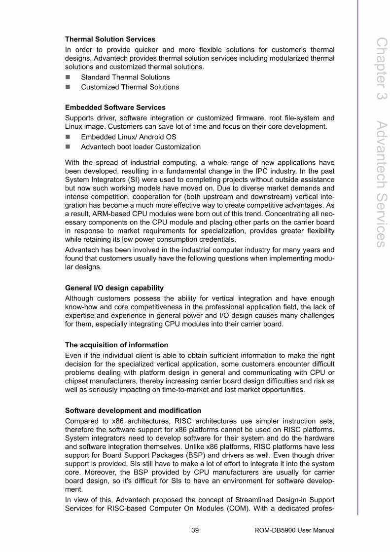
2.4.6 LEDs
2.4.7 Hardware installation1. Install the ROM-5420 module board to carrier board at a 30 degree angle.
Position Function Position Function
D25 VIN_PWR_BAD# D26 +VDC_SYS
D27 Carrier_PWR_ON D28 +12V
D29 Carrier_STBY# D30 +5V
D31 +3V
ROM-DB5900 User Manual 34

Chapter 2
H/W
Installation
2. Press down the module board and make sure the 4 screw holes are aligned with the carrier board and adjust the 4 screws clockwise to fix them in place
35 ROM-DB5900 User Manual

ROM-DB5900 User Manual 36

Chapter 3
3 Advantech ServicesThis chapter introduces Advan-tech design in serviceability, tech-nical support and warranty policy for ROM-DB5900.
3.1 RISC Design-in Services
Advantech RISC Design-in Services help customers to reduce the time and workinvolved with designing new carrier boards. We handle the complexities of technicalresearch and greatly minimize the development risk associated with carrier boards.
Easy Development
Advantech provides support for firmware, root file-system, BSP or other developmenttools for customers. These help customers to easily develop their carrier boards anddifferentiate their embedded products and applications.
Full Range of RISC Product Offerings Comprehensive Document Support
Design Assistance Service
Advantech provides check list for engineer for easy check their schematics and alsoreview service based on customer carrier board schematics. Those services are pre-ventative, and help to catch design errors before they happen. It helps to save a lot oftime and costs with regard to developing carrier boards.
Schematic Review Placement and Layout Review Debugging Assistance Services General/Special Reference Design Database.
ROM-DB5900 User Manual 38
Chapter 3
Advantech
Services
Thermal Solution Services
In order to provide quicker and more flexible solutions for customer's thermaldesigns. Advantech provides thermal solution services including modularized thermalsolutions and customized thermal solutions.
Standard Thermal Solutions Customized Thermal Solutions
Embedded Software Services
Supports driver, software integration or customized firmware, root file-system andLinux image. Customers can save lot of time and focus on their core development.
Embedded Linux/ Android OS Advantech boot loader Customization
With the spread of industrial computing, a whole range of new applications havebeen developed, resulting in a fundamental change in the IPC industry. In the pastSystem Integrators (SI) were used to completing projects without outside assistancebut now such working models have moved on. Due to diverse market demands andintense competition, cooperation for (both upstream and downstream) vertical inte-gration has become a much more effective way to create competitive advantages. Asa result, ARM-based CPU modules were born out of this trend. Concentrating all nec-essary components on the CPU module and placing other parts on the carrier boardin response to market requirements for specialization, provides greater flexibilitywhile retaining its low power consumption credentials.
Advantech has been involved in the industrial computer industry for many years andfound that customers usually have the following questions when implementing modu-lar designs.
General I/O design capability
Although customers possess the ability for vertical integration and have enoughknow-how and core competitiveness in the professional application field, the lack ofexpertise and experience in general power and I/O design causes many challengesfor them, especially integrating CPU modules into their carrier board.
The acquisition of information
Even if the individual client is able to obtain sufficient information to make the rightdecision for the specialized vertical application, some customers encounter difficultproblems dealing with platform design in general and communicating with CPU orchipset manufacturers, thereby increasing carrier board design difficulties and risk aswell as seriously impacting on time-to-market and lost market opportunities.
Software development and modification
Compared to x86 architectures, RISC architectures use simpler instruction sets,therefore the software support for x86 platforms cannot be used on RISC platforms.System integrators need to develop software for their system and do the hardwareand software integration themselves. Unlike x86 platforms, RISC platforms have lesssupport for Board Support Packages (BSP) and drivers as well. Even though driversupport is provided, SIs still have to make a lot of effort to integrate it into the systemcore. Moreover, the BSP provided by CPU manufacturers are usually for carrierboard design, so it's difficult for SIs to have an environment for software develop-ment.
In view of this, Advantech proposed the concept of Streamlined Design-in SupportServices for RISC-based Computer On Modules (COM). With a dedicated profes-
39 ROM-DB5900 User Manual

sional design-in services team, Advantech actively participates in carrier boarddesign and problem solving. Our services not only enable customers to effectivelydistribute their resources but also reduce R&D manpower cost and hardware invest-ment.
By virtue of a close interactive relationship with leading original manufacturers ofCPUs and chipsets such as ARM, TI and Freescale, Advantech helps solve commu-nication and technical support difficulties, and that can reduce the uncertainties ofproduct development too. Advantech's professional software team also focuses onproviding a complete Board Support Package and assists customers to build up asoftware development environment for their RISC platforms.
Advantech RISC design-in services helps customers overcome their problems toachieve the most important goal of faster time to market through a streamlined RISCDesign-in services.
Along with our multi-stage development process which includes: planning, design,integration, and validation, Advantech's RISC design-in service provides comprehen-sive support to the following different phases:
Planning stage
Before deciding to adopt Advantech RISC COM, customers must go through a com-plete survey process, including product features, specification, and compatibility test-ing with software. So, Advantech offers a RISC Customer Solution Board (CSB) asan evaluation tool for carrier boards which are simultaneously designed when devel-oping RISC COMs. In the planning stage, customers can use this evaluation board toassess RISC modules and test peripheral hardware. What's more, Advantech pro-vides standard software Board Support Package (BSP) for RISC COM, so that cus-tomers can define their product's specifications as well as verifying I/O andperformance at the same time. We not only offer hardware planning and technologyconsulting, but also software evaluation and peripheral module recommendations(such as WiFi, 3G, BT). Resolving customer concerns is Advantech's main target atthis stage. Since we all know that product evaluation is the key task in the planningperiod, especially for performance and specification, so we try to help our customersconduct all the necessary tests for their RISC COM.
Design stage
When a product moves into the design stage, Advantech will supply a design guide ofthe carrier board for reference. The carrier board design guide provides pin defini-tions of the COM connector with limitations and recommendations for carrier boarddesign, so customers can have a clear guideline to follow during their carrier boarddevelopment. Regarding different form factors, Advantech offers a complete pin-outcheck list for different form factors such as Q7, ULP and RTX2.0, so that customerscan examine the carrier board signals and layout design accordingly. In addition, ourteam is able to assist customers to review the placement/layout and schematics toensure the carrier board design meets their full requirements. For software develop-ment, Advantech RISC software team can assist customers to establish an environ-ment for software development and evaluate the amount of time and resourcesneeded. If customers outsource software development to a 3rd party, Advantech canalso cooperate with the 3rd party and provide proficient consulting services. WithAdvantech's professional support, the design process becomes much easier andproduct quality will be improved to meet their targets.
ROM-DB5900 User Manual 40
Chapter 3
Advantech
Services
Integration stage
This phase comprises of HW/SW integration, application development, and periph-eral module implementation. Due to the lack of knowledge and experience on plat-forms, customers need to spend a certain amount of time on analyzing integrationproblems. In addition, peripheral module implementation has a lot to do with driverdesigns on carrier boards, RISC platforms usually have less support for ready-madedrivers on the carrier board, therefore the customer has to learn from trial and errorand finally get the best solution with the least effort. Advantech's team has years ofexperience in customer support and HW/SW development knowledge. Conse-quently, we can support customers with professional advice and information as wellas shortening development time and enabling more effective product integration.
Validation stage
After customer's ES sample is completed, the next step is a series of verificationsteps. In addition to verifying a product's functionality, the related test of the product'sefficiency is also an important part at this stage especially for RISC platforms.
As a supportive role, Advantech primarily helps customers solve their problems in thetesting process and will give suggestions and tips as well. Through an efficient verifi-cation process backed by our technical support, customers are able to optimize theirapplications with less fuss. Furthermore, Advantech's team can provide professionalconsulting services about further testing and equipment usage, so customers canfind the right tools to efficiently identify and solve problems to further enhance theirproducts quality and performance.
3.2 Contact InformationBelow is the contact information for Advantech customer service.
On the other hand, you can reach our service team through below website, our tech-nical support engineer will provide quick response once the form is filled out:
http://www.advantech.com.tw/contact/default.aspx?page=contact_form2&sub-ject=Technical+Support
Region/Country Contact Information
America 1-888-576-9688
Brazil 0800-770-5355
Mexico 01-800-467-2415
Europe (Toll Free) 00800-2426-8080
Singapore & SAP 65-64421000
Malaysia 1800-88-1809
Australia (Toll Free) 1300-308-531
China (Toll Free)[email protected]
India (Toll Free) 1-800-425-5071
Japan (Toll Free) 0800-500-1055
Korea (Toll Free) 080-363-9494
080-363-9495
Taiwan (Toll Free) 0800-777-111
Russia (Toll Free) 8-800-555-01-50
41 ROM-DB5900 User Manual

3.3 Technical Support and AssistanceFor more information about this and other Advantech products, please visit our web-site at:
<http://www.advantech.com/>
<http://www.advantech.com/ePlatform/>
For technical support and service, please visit our support website at:
<http://support.advantech.com.tw/support/>
1. Visit the Advantech web site at www.advantech.com/support where you can find the latest information about the product.
2. Contact your distributor, sales representative, or Advantech's customer Service center for technical support if you need additional assistance. Please have the following information ready before you call:- Product name and serial number
- Description of your peripheral attachments
- Description of your software (operating system, version, application software,etc.)
- A complete description of the problem
- The exact wording of any error messages
3.4 Global Service Policy
3.4.1 Warranty PolicyBelow is the warranty policy of Advantech products:
3.4.2 Warranty PeriodAdvantech branded off-the-shelf products and 3rd party off-the-shelf products used toassemble Advantech Configure to Order products are entitled to a 2 years completeand prompt global warranty service. Product defect in design, materials, and work-manship, are covered from the date of shipment.
All customized products will by default carry a 15 months regional warranty service.The actual product warranty terms and conditions may vary based on sales contract.
All 3rd party products purchased separately will be covered by the original manufac-turer's warranty and time period, and shall not exceed one year of coverage throughAdvantech.
3.4.3 Repairs under WarrantyIt is possible to obtain a replacement (Cross-Shipment) during the first 30 days of thepurchase, thru your original ADVANTECH supplier to arrange DOA replacement ifthe products were purchased directly from ADVANTECH and the product is DOA(Dead-on-Arrival). The DOA Cross-Shipment excludes any shipping damage, cus-tomized and/or build-to-order products.
For those products which are not DOA, the return fee to an authorized ADVANTECHrepair facility will be at the customers' expense. The shipping fee for reconstructiveproducts from ADVANTECH back to customers' sites will be at ADVANTECH'sexpense.
ROM-DB5900 User Manual 42
Chapter 3
Advantech
Services
3.4.4 Exclusions from WarrantyThe product is excluded from warranty if
The product has been found to be defective after expiry of the warranty period. Warranty has been voided by removal or alternation of product or part identifica-
tion labels. The product has been misused, abused, or subjected to unauthorized disas-
sembly/modification; placed in an unsuitable physical or operating environment; improperly maintained by the customer; or failure caused which ADVANTECH is not responsible whether by accident or other cause. Such conditions will be determined by ADVANTECH at its sole unfettered discretion.
The product is damaged beyond repair due to a natural disaster such as a light-ing strike, flood, earthquake, etc.
Product updates/upgrades and tests upon the request of customers who are without warranty.
3.5 Repair Process
3.5.1 Obtaining an RMA NumberAll returns from customers must be authorized with an ADVANTECH RMA (ReturnMerchandise Authorization) number. Any returns of defective units or parts withoutvalid RMA numbers will not be accepted; they will be returned to the customer at thecustomer's cost without prior notice.
An RMA number is only an authorization for returning a product; it is not an approvalfor repair or replacement. When requesting an RMA number, please access ADVAN-TECH's RMA web site: http://erma.ADVANTECH.com.tw with an authorized user IDand password.
You must fill out basic product and customer information and describe the problemsencountered in detail in "Problem Description". Vague entries such as "does notwork" and "failure" are not acceptable.
If you are uncertain about the cause of the problem, please contact ADVANTECH'sApplication Engineers (AE). They may be able to find a solution that does not requiresending the product for repair.
The serial number of the whole set is required if only a key defective part is returnedfor repair. Otherwise, the case will be regarded as out-of-warranty.
3.5.2 Returning the Product for RepairIt's possible customers can save time and meet end-user requirements by returningdefective products to an authorized ADVANTECH repair facility without an extracross-region charge. It is required to contact the local repair center before offeringglobal repair service.
It is recommended to send cards without accessories (manuals, cables, etc.).Remove any unnecessary components from the card, such as CPU, DRAM, and CFCard.If you send all these parts back (because you believe they may be part of theproblem), please note clearly that they are included. Otherwise, ADVANTECH is notresponsible for any items not listed. Make sure the "Problem Description" isenclosed.
European Customers that are located outside European Community are requested touse UPS as the forwarding company. We strongly recommend adding a packing listto all shipments.Please prepare a shipment invoice according to the following guide-lines to decrease goods clearance time:
43 ROM-DB5900 User Manual

1. Give a low value to the product on the invoice, or additional charges will be lev-ied by customs that will be borne by the sender.
2. Add information "Invoice for customs purposes only with no commercial value" on the shipment invoice.
3. Show RMA numbers, product serial numbers and warranty status on the ship-ment invoice.
4. Add information about Country of origin of goodsIn addition, please attach an invoice with RMA number to the carton, then write theRMA number on the outside of the carton and attach the packing slip to save han-dling time. Please also address the parts directly to the Service Department and markthe package "Attn. RMA Service Department".
All products must be returned in properly packed ESD material or anti-static bags.ADVANTECH reserves the right to return un-repaired items at the customer's cost ifinappropriately packed.
What’s more, "Door-to-Door" transportation such as speed post is recommended fordelivery, otherwise, the sender should bear additional charges such as clearancefees if Air-Cargo is adopted.
Should DOA cases fail, ADVANTECH will take full responsibility for the product andtransportation charges. If the items are not DOA, but fail within warranty, the senderwill bear the freight charges. For out-of-warranty cases, customers must cover thecost and take care of both outward and inward transportation.
3.5.3 Service ChargesThe product is excluded from warranty if:
The product is repaired after expiry of the warranty period. The product is tested or calibrated after expiry of the warranty period, and a No
Problem Found (NPF) result is obtained. The product, though repaired within the warranty period, has been misused,
abused, or subjected to unauthorized disassembly/modification; placed in an unsuitable physical or operating environment; improperly maintained by the cus-tomer; or failure caused which ADVANTECH is not responsible whether by acci-dent or other cause. Such conditions will be determined by ADVANTECH at its sole unfettered discretion.
The product is damaged beyond repair due to a natural disaster such as a light-ing strike, flood, earthquake, etc.
Product updates and tests upon the request of customers who are without war-ranty.
If a product has been repaired by ADVANTECH, and within three months after such arepair the product requires another repair for the same problem, ADVANTECH will dothis repair free of charge. However, such free repairs do not apply to products whichhave been misused, abused, or subjected to unauthorized disassembly/modification;placed in an unsuitable physical or operating environment; improperly maintained bythe customer; or failure caused which ADVANTECH is not responsible whether byaccident or other cause.
Please contact your nearest regional service center for detail service quotation.
Before we start out-of-warranty repairs, we will send you a pro forma invoice (P/I)with the repair charges. When you remit the funds, please reference the P/I numberlisted under "Our Ref". ADVANTECH reserves the right to deny repair services tocustomers that do not return the DOA unit or sign the P/I. Meanwhile, ADVANTECHwill scrap defective products without prior notice if customers do not return the signedP/I within 3 months.
ROM-DB5900 User Manual 44

Chapter 3
Advantech
Services
3.5.4 Repair ReportADVANTECH returns each product with a "Repair Report" which shows the result ofthe repair. A "Repair Analysis Report" is also provided to customers upon request. Ifthe defect is not caused by ADVANTECH design or manufacturing, customers will becharged US$60 or US$120 for in-warranty or out-of-warranty repair analysis reportsrespectively.
3.5.5 Custody of Products Submitted for RepairADVANTECH will retain custody of a product submitted for repair for one month whileit is waiting for return of a signed P/I or payment (A/R). If the customer fails torespond within such period, ADVANTECH will close the case automatically. ADVAN-TECH will take reasonable measures to stay in proper contact with the customer dur-ing this one month period.
3.5.6 Shipping Back to CustomerThe forwarding company for RMA returns from ADVANTECH to customers isselected by ADVANTECH. Per customer requirement, other express services can beadopted, such as UPS, FedEx etc. The customer must bear the extra costs of suchalternative shipment. If you require any special arrangements, please indicate thiswhen shipping the product to us.
45 ROM-DB5900 User Manual

www.advantech.comPlease verify specifications before quoting. This guide is intended for referencepurposes only.All product specifications are subject to change without notice.No part of this publication may be reproduced in any form or by any means,electronic, photocopying, recording or otherwise, without prior written permis-sion of the publisher.All brand and product names are trademarks or registered trademarks of theirrespective companies.© Advantech Co., Ltd. 2014