user’s manual - build your own microcontroller projects · user’s manual 8051 project board ......
TRANSCRIPT


Contents
1. Overview2. Getting started3. Using Mikro-c for 80514. Example of c programs
SchematicBill of Materials (BOM)
1. Overview
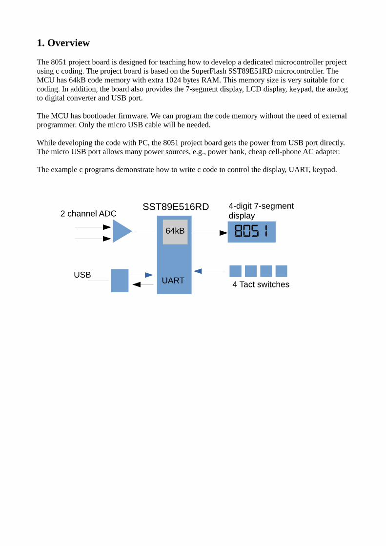
The 8051 project board is designed for teaching how to develop a dedicated microcontroller project using c coding. The project board is based on the SuperFlash SST89E51RD microcontroller. The MCU has 64kB code memory with extra 1024 bytes RAM. This memory size is very suitable for c coding. In addition, the board also provides the 7-segment display, LCD display, keypad, the analogto digital converter and USB port.
The MCU has bootloader firmware. We can program the code memory without the need of external programmer. Only the micro USB cable will be needed.
While developing the code with PC, the 8051 project board gets the power from USB port directly. The micro USB port allows many power sources, e.g., power bank, cheap cell-phone AC adapter.
The example c programs demonstrate how to write c code to control the display, UART, keypad.
8051
2 channel ADCSST89E516RD 4-digit 7-segment
display
4 Tact switchesUARTUSB
64kB

Basic layout
Basic components are:
1. SST89E51RD, 40-pin Microcontroller.2. 4-digit 7-segment display.3. USB-UART interface chip, CH340G4. Tact switch keypad.5. Micro-USB cable

2. Getting started
Students will need PC, or Notebook computer with USB port. The PC will run c compiler program and EasyIAP for hex code downloading.
The UART-USB device, CH340G will need the hardware driver.
Step 1 Download and install the driver.
http://www.kswichit.com/Flashflex/images/CH34x_Install_Windows_v3_4.zip
When connect the project board to the PC USB port, the hardware manager will assign the COM port number automatically.
We can modify the COM port number easily by right click, properties/port settings/advance.
The example was set it to COM2.

We can test communication between the PC and project board by using the EasyIAP program.
Step 2 Download and install the EasyIAP.
http://www.kswichit.com/Flashflex/EasyIAP%20Rev%206.0.zip
Run the EasyIAP. Click Option.
Select COM2, and SST89E51RD chip.

Press RESET button on the project board.
Then CLICK OK, and release RESET button immediately!
The EasyIAP will connect the project board and display chip information.
The IAP Status shows Detect target MCU is successful!

Click Read right-hand, the code memory will be read. We can see the buffer memory window. It shows the memory contents in HEX number.

How to write the hex code to the MCU.
Now let us try program the MCU with hex code.
Download the hex file http://www.kswichit.com/Flashflex/images/scan2.hex
We will try using the EasyIAP to program this hex code the MCU.
Step 4 Reconnect the project board with Connect click again.
Click Dnload/Run UserCode 1.
Then Click the hex file 2.

Then Click YES, the corresponding sectors will be erased.
After completed, the CPU will jump from bootloader to user code.
We will see the display showing 8051.

Can we change the display from 8051 to any text? How?
Now press RESET and connect the project board to the EasyIAP again.
Then click Read.
We see that the bytes that contain pattern 8051 are.
Location 00A1 = 06 for “1”Location 00A4 = 6D for “5”Location 00A7 = 3F for “0”Location 00AA = 7F for “8”
The bit pattern for 7-segment display is shown below.
/* 7-segment pattern converting array
a __ register data
f |__| b D7 D6 D5 D4 D3 D2 D1 D0
e |__| c .DP DP g f e d c b a
d*/

We can modify those bytes easily with Menu, ByteModify
1. Enter location to be modified.
2. Click Display Data.
3. Copy the hex byte.
4. Paste it to New data, then modify from 7F to 3F or any hex value 00-FF.
5. Then Click Replace Data.
The click RESET on the board, see what is happening?
3. Using Mikro-C for 8051 compiler
Mikro-c for 8051 is very suitable for our kit. The demo provides fully functional for a limited code size. It can be downloaded here, https://www.mikroe.com/mikroc/
Let us try building the simple c code for testing the boot loader.
The kit has one debug LED connected to P1.2.
/*Test code led blinking at P1.2 MCU : AT89C51RD2 OSC: 12MHz */
void main() {
while(1) { P1 ^= 0x04; Delay_ms(500); // 0.5 second delay }}
This simple c code will make the debug LED blinks.
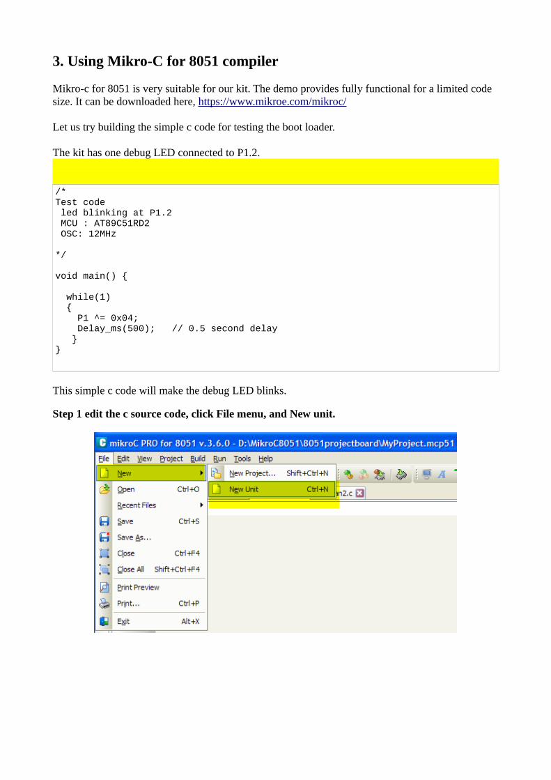
Step 1 edit the c source code, click File menu, and New unit.

Edit c source code and save it as blink.c
We have c source code, now we will create project file then add this source code to the project file.
Step 2 Create project file, set project name 1, select AT89C51RD2 2, and set Clock 12MHz 3.

Step 3 select memory model SMALL for single chip operation.
Step 3 Add the c source code to the project
To build the project or translate the c source code to assembly code and finally to the hex code, click Build or Ctrl-F9.
The compiler will generate assembly code and Intel hex file ready for programming by EasyIAP.

4. Example of c programs
Let us try using the Mikro-c for 8051 by editing the c program, add it to the project file, build the project and finally load the hex code to the 8051 project board.
Source code of the c programs can be downloaded at,
http://www.kswichit.com/Flashflex/projectbo ardsst.html
Program 1 LED blinking
/*Test code led blinking at P1.2 MCU : AT89C51RD2 OSC: 12MHz */
void main() {
while(1) { P1 ^= 0x04; Delay_ms(500); // 0.5 second delay }
The LED that tied to P1.2 bit is turned on when the logic at P1.2 is LOW. We toggle P1.2 by using exclusive OR, delay then repeat the loop.
Can you change blinking rate? How?

Program 2 Scanning 7-segment display
/*Test code seven segment test code MCU : AT89C51RD2 OSC: 12MHz
*/
#define segment P0#define digit P2
void main() {
while(1) { digit = ~0x08; P0 = 0x7f; Delay_ms(300); // 0.5 second delay digit = ~0x04; P0 = 0x7f; Delay_ms(300); // 0.5 second delay digit = ~0x02; P0 = 0x7f; Delay_ms(300); // 0.5 second delay
digit = ~0x01; P0 = 0x7f; Delay_ms(300); // 0.5 second delay }}
Refer to schematic details, we make each digit turn ON one by one.
Did you see display blinking?
Can you make still display? How?
Can you make display “HOLA”? How?

Program 3 Use Timer2 for 9600 BAUD generation
// test CH340G with UART using timer 2 for baud rate generation
char c;sbit LED at P1.B2;
// using timer2 for 9600 bit/s with 12MHz oscillatorvoid init_UART(){ T2CON = 0x30; RCAP2H = 0xFF; RCAP2L = 0xd9; SCON = 0x50; TR2_bit =1;}
void main() {
init_UART(); Delay_ms(100); c = 0x20; // UART1_Write_Text("Start"); while (1) { LED = 0; UART1_Write_Text("\r\n8051 Project board"); LED = 1; Delay_ms(500); } }}
The kit uses a 12MHz oscillator. Our code initializes the serial port by using Timer2 for 9600 bit/s.
To test it, we must close the EasyIAP and run terminal emulator software. Set it to 9600 bit/s.
Can you change message sent to the terminal? How?

Program 4 Scan display and keypad
/*Test code scan display and keypad MCU : AT89C51RD2 OSC: 12MHz*/
/* 7-segment pattern converting array a __ register data f |__| b D7 D6 D5 D4 D3 D2 D1 D0 e |__| c.DP DP g f e d c b a d*/
const char convert[10] = {0x3f,0x06,0x5b,0x4f,0x66,0x6d,0x7d,0x07,0x7f,0x6f};
char buffer[4]; // display buffer memorychar i,j,k;char key;
char scan(){ key = 0xff; j = 0x08; for(i=0; i<4; i++) { P2 = ~j; // select digit P0 = buffer[i]; // write segment Delay_ms(5); if((P2&0x10) == 0) key = i; // if key pressed, save #key P0 = 0; j>>=1; // next digit
} return key; // return key code}
void main() {
buffer[0] = 0x06; buffer[1] = 0x6d; buffer[2] = 0x3f; buffer[3] = 0x7f; while(1) { while(scan()!= 0xff) ; Delay_ms(10); while(scan()== 0xff) ; Delay_ms(10); k=scan();
switch(k) { case 0: P1 = 0; break; case 1: P1 = 0xff; break;

// case 2: show2(); break; // case 3: show3(); break; } }}
More complicated scanning the display and keypad, will display byte pattern in buffer memory and return key code if pressed.
Press SW4 then SW3 what is happening?
Can you move the functions that turn ON/FF debug LED to SW2 and SW1? How?

Program 5 Display number with time to buffer function.
/*Test code display number on 7-segment MCU : AT89C51RD2 OSC: 12MHz*/
/* 7-segment pattern converting array a __ register data f |__| b D7 D6 D5 D4 D3 D2 D1 D0 e |__| c.DP DP g f e d c b a d*/
code char convert[10] = {0x3f,0x06,0x5b,0x4f,0x66,0x6d,0x7d,0x07,0x7f,0x6f};
char buffer[4]; // display buffer memorychar i,j,k;char key;char second,minute;
char scan(){ key = 0xff; j = 0x08; for(i=0; i<4; i++) { P2 = ~j; // select digit P0 = buffer[i]; // write segment Delay_ms(5); if((P2&0x10) == 0) key = i; // if key pressed, save #key P0 = 0; j>>=1; // next digit
} return key; // return key code}
void time2buffer(){ buffer[1]= convert[second/10]; buffer[0]= convert[second%10]; buffer[3]= convert[minute/10]; buffer[2]= convert[minute%10]|0x80;}
void main() {
second = 59; minute = 30; time2buffer(); // convert sec and min to buffer memory while(1)

{ while(scan()!= 0xff) ; Delay_ms(10); while(scan()== 0xff) ; Delay_ms(10); k=scan();
switch(k) { case 0: P1 = 0; break; case 1: P1 = 0xff; break; // case 2: show2(); break; // case 3: show3(); break; } }}
The value in minute and second variables are converted to display pattern using array convert.
Can you change the number to be displayed? How?
Explain below statements.
buffer[1]= convert[second/10]; buffer[0]= convert[second%10];

Program 6 LCD display interface by 4-bit mode
// Lcd module connectionssbit LCD_RS at P2_6_bit;sbit LCD_EN at P2_7_bit;sbit LCD_RW at P2_5_bit; // must be low
sbit LCD_D4 at P0_4_bit;sbit LCD_D5 at P0_5_bit;sbit LCD_D6 at P0_6_bit;sbit LCD_D7 at P0_7_bit;// End Lcd module connections
char txt1[] = "8051 PROJECT KIT";
char txt2[] = "Hello Boy";
char txt3[] = "Lcd4bit";char txt4[] = "Interface";
char i; // Loop variable
void Move_Delay() { // Function used for text moving Delay_ms(500); // You can change the moving speed here}
void main(){
P0= 0; LCD_RW =0; Lcd_Init(); // Initialize Lcd
Lcd_Cmd(_LCD_CLEAR); // Clear display Lcd_Cmd(_LCD_CURSOR_OFF); // Cursor off Lcd_Out(1,6,txt3); // Write text in first row
Lcd_Out(2,6,txt4); // Write text in second row Delay_ms(2000); Lcd_Cmd(_LCD_CLEAR); // Clear display
Lcd_Out(1,1,txt1); // Write text in first row Lcd_Out(2,5,txt2); // Write text in second row
Delay_ms(2000);
// Moving text for(i=0; i<4; i++) { // Move text to the right 4 times Lcd_Cmd(_LCD_SHIFT_RIGHT); Move_Delay(); }
while(1) { // Endless loop for(i=0; i<8; i++) { // Move text to the left 7 times Lcd_Cmd(_LCD_SHIFT_LEFT); Move_Delay(); }
for(i=0; i<8; i++) { // Move text to the right 7 times Lcd_Cmd(_LCD_SHIFT_RIGHT); Move_Delay(); }

}}
The 16x2 text LCD will be installed on JR1 connector. Adjust R3 for LCD contrast.
We use the Mikro-c library for 4-bit LCD interface. Only D4-D7 will be needed for data writing.
Can you change message to be display? How?

Program 7 Digital CLOCK using timer0 intetrrupt
/* Example code for digital clock using timer0 interrupt with 10ms tick MCU : AT89C51RD2 OSC: 12MHz*/
/* 7-segment pattern converting array a __ register data f |__| b D7 D6 D5 D4 D3 D2 D1 D0 e |__| c.DP DP g f e d c b a d*/
char code convert[10] = {0x3f,0x06,0x5b,0x4f,0x66,0x6d,0x7c,0x07,0x7f,0x67};char buffer[4]; // display bufferchar i,j,k;char min_key;char hour_key;char pressed;char command;char sec10,second,minute,hour;char blink_tick;char blink;char state; // state =0 turn off all outputs // state =1 normal clock running, initiate when any keys were pressed char temp;char key;sbit LED at P1.B2;
char scan(){ key = 0xff; j = 0x08; for(i=0; i<4; i++) { P2 = ~j; // select digit P0 = buffer[i]; // write segment Delay_ms(5); if((P2&0x10) == 0) key = i; // if key pressed, save #key P0 = 0; j>>=1; // next digit
} return key; // return key code}
void print_time() { buffer[0]= convert[minute%10]; buffer[1]= convert[minute/10]; buffer[2]= convert[hour%10]|0x80; buffer[3]= convert[hour/10]; if(buffer[3]== 0x3F) buffer[3]=0; // turn off zero
}

void time() { if(++sec10==100) { sec10 =0; print_time(); blink=1;
if ( ++second >= 60) { second = 0;
if ( ++minute >= 60) { minute = 0;
if ( ++hour >= 24) hour = 0; } } }
}
void Timer0InterruptHandler() org IVT_ADDR_ET0{ TH0 = 0xD8; // Reset Timer1 high byte TL0 = 0xF0; // reload 0xD8F0 time(); // update realtime clock if(blink) { if(++blink_tick >50) { blink=0; blink_tick=0; buffer[2]&= ~0x80; } }
}
void release_key() { if((scan()==0xff) && (pressed==1)) { pressed=0; Delay_ms(5); } }
void set_hour() { if((scan()==0) && (pressed==0)) { pressed=1; state=1; print_time(); if(++hour >=24)hour =0;

} }
void set_min() { if((scan()==1) && (pressed==0)) {
second =0; pressed=1; state=1; print_time(); if(++minute>59) minute =0;
}}
void main() {
EA_bit = 0; ET0_bit = 1; // set bit EA and Timer0 enable
TMOD = 0x01; // timer 1 TR0_bit = 1; // run timer0
hour = 8; // when reset set current time to 8:00 minute = 0; second = 0; state=0;
buffer[0]=0x40; buffer[1]=0x40; buffer[2]=0x40; buffer[3]=0x40; pressed=0;
while(1) { switch(state) { case 0: scan(); set_hour(); set_min(); release_key(); break; case 1: EA_bit = 1; // run clock scan(); set_hour(); set_min(); release_key(); break; }

}}
The CLOCK program uses timer0 running 16-bit counter. The timer clock is 12MHz/12= 1MHz.
To produce 10ms tick or 100Hz interrupt rate, the CPU must count 1x10⁶/100 = 10000. Using timer0 16-bit counter, the number of count will be 65536-10000= 55536 or 0xD8F0.
Every 10ms tick, the service for timer0 interrupt will be entered. The time will be updated.
The clock variables will be converted into display pattern by print_time() function.
Pressing keypad, SW4 will update HOUR, SW3 will update MIN.
Can you add function that makes DEBUG LED ON at 20:00 and turn OFF at 23:00? How?

55
44
33
22
11
DD
CC
BB
AA
+5V
ADC0
RS
GND
R/W
ADC1
E
External +5V USB powerAdapter/PowerBank/SolarUSB/USBrealtime data
UART to USB
10-pin USBaspLoader
Designed by Wichit Sirichote, [email protected] (C) 2017
<Doc>
1
8051 PR
OJE
CT
BO
ARD
V1.0
Custom
11
Monday, S
eptember 25, 2017
Title
Size
Docum
ent Num
berR
ev
Date:
Sheet
of
P3.2/IN
T0
D3
P1.1/T
2-EX
D0
DIG
IT1
SC
K
P3.2/IN
T0
P1.1/T
2-EX
D1
DIG
IT4RS
P3.4/T
0
D2
D7
DIG
IT2
CS
KE
Y_P
RE
SS
P1.2
D6
E
D4
ADC
DAT
A
D5
P3.4/T
0
XTAL1
MO
SI
D1
D2
P3.3/IN
T1
P1.0/T
2T
XD
P1.3
12MH
zXT
AL2
P1.0/T
2
MIS
O DIG
IT3RW
D6
D5
P3.3/IN
T1
D4
SC
K
RXD
RS
RW
XTAL1
P1.2
P3.5/T
1
E
RE
SE
T D0
P1.3
D3
P3.7
CS
P3.7
P3.5/T
1
XTAL2
D7
ADC
DAT
A
D4
D2
D0
D6
D1
D7
D5
D3
DIG
IT2
DIG
IT3
DIG
IT4
KE
Y_P
RE
SS
DIG
IT1
D5
D2
D3
D7
D6
D0
D1
D4
12MH
z
TXD
+5VUS
B
+5VUS
BR
XD
UD
+
UD
-
+5VUS
B
MO
SI
MIS
OS
CK
MO
SI
RE
SE
TS
CK
MIS
O
VCC
VCC
VCC
VCC
VCC
VCC
VCC
VCC
VCC
VCC
VCC
U2SS
T59E
516RD
/AT89S
52
9 18 192930
31
40
12345678
21222324252627281011121314151617
3938373635343332
RS
TXT
AL2XT
AL1P
SE
N
ALE/P
RO
G
EA/VP
P
VCC
P1.0/T
2P
1.1/T2-E
XP
1.2P
1.3P
1.4P
1.5/MO
SI
P1.6/M
ISO
P1.7/S
Ck
P2.0/A8
P2.1/A9
P2.2/A10
P2.3/A11
P2.4/A12
P2.5/A13
P2.6/A14
P2.7/A15
P3.0/R
XDP
3.1/TXD
P3.2/IN
TO
P3.3/IN
T1
P3.4/T
OP
3.5/T1
P3.6/W
RP
3.7/RD
P0.0/AD
0P
0.1/AD1
P0.2/AD
2P
0.3/AD3
P0.4/AD
4P
0.5/AD5
P0.6/AD
6P
0.7/AD7
U3
MC
3202
1 5 678
23
CS
/SH
DN
DIN
DO
UT
CLK
VCC
CH
0
CH
1
D21N
5231B 5.1Vz 1/2W
J3CO
N6
123456
+
C10
100uF 16V
C11
0.1uF
+C
5100uF
C9
100nF
U4CH
340G
16417856 23
15
VCC
V3GN
D
XIXOU
D+
UD
-
TXD
RXD
RS
232
R8100
SW
2
12
JR1
CO
NN
RE
CT
16
1 2 3 4 5 6 7 8 9 10 11 12 13 14 15 16
1 2 3 4 5 6 7 8 9 10 11 12 13 14 15 16
D-D+ +5V
GND
CN
1M
ICR
O-U
SB
1234
5
SW
3
12
+
C4
10uF 16V
SW
4
12
S1
RE
SE
T
J2
13579111315
246810121416
++++++++
++++++++
TP
1
+5V 1
TP
2
GN
D
1
C
R4
1k RE
SIS
TO
R S
IP 9
123456789
C6
100nF
J1CO
N10AP
13579
246810
+++++
+++++
R6
100
R7
100
+C
310uF
R3
10K
13
2
R5
10k
C12
100nF
Q1
12MH
z
SW
1
12
C7
0.1uF
D1DE
BU
G LE
D
C8
0.1uF
C1
30pF
R2
5
R1
330C
2
30pF
U1LT
C-4727JR
1416133511157
1
2
6
8
4
ABCDEFGDP
DIGIT1
DIGIT2
DIGIT3
DIGIT4
L1L2L3

8051BOARD
Page 1
8051 PROJECT BOARD V1.0 Revised: Monday, September 25, 2017 Revision: 1Bill Of Material Page1
Item Quantity Reference Part Chk______________________________________________
1 1 CN1 MICRO-USB connector2 2 C1,C2 30pF ceramic cap3 1 C3 10uF 16V electrolytic capacitor4 1 C4 10uF 16V5 1 C5 10uF electrolytic capacitor6 3 C6,C9,C12 100nF7 3 C7,C8,C11 0.1uF8 1 C10 10uF 16V9 1 D1 3mm LED
10 1 D2 1N5231B 5.1Vz 1/2W zener diode11 1 JR1 Header 16-pin12 1 J1 CON10AP13 1 J2 CON16AP14 1 J3 CON615 1 Q1 12MHz xtal16 1 R1 Ohms 330 1/8W 5%17 1 R2 Ohms 5 1/8W 5%18 2 R3,R5 10k 1/8W 5%19 1 R4 1k RESISTOR SIP 920 3 R6,R7,R8 Ohms 100 1/8W 5%21 4 SW1,SW2,SW3,SW4 12x12 TACT switch22 1 S1 6x6 TACT switch RESET23 1 TP1 +5V24 1 TP2 GND25 1 U1 LTC-4727JR26 1 U2 SST89E516RD + 40 pins socket27 1 U3 MCP3202 12-bit ADC + 8 pins socket28 1 U4 CH340G USB-UART chip29 1 PCB Printed Circuit Board