user’s manual - nxp semiconductors | automotive ... · section 4, “programmers model” 12 ......
TRANSCRIPT
User’s Manual
MVPX2UM/DRev. 0.4, 11/2001
MVP X2 RISC Microprocessor Evaluation Platform User’s Manual
CPD Applications
Welcome to MVP, Motorola’s Multi-processing Verification Platform.MVP is a hardware and software development platform which can be used to evaluate theperformance and features of a multi-processing system using Motorola microprocessorswhich implement the PowerPC architecture.
This User’s Manual covers the following issues:
Topic Page
Section 2, “Setup” 3
Section 3, “Configuration” 5
Section 4, “Programmers Model” 12
Section 5, “Development Issues” 16
Section 6, “Other Information” 20
To locate any published errata or updates for this document, refer to the website athttp://www.mot.com/SPS/RISC/smartnetworks/.

Introduction
1.1 IntroductionThe Multi-processing Verification Platform, or “MVP” for short, is an evaluation board which contains twoMPC7450 “V’ger” processors coupled with the Marvell GT64260 Memory/PCI Controller. In additionMVP contains four PCI slots and a VIA PIPC providing USB, IDE and other typical PC I/O peripherals.Figure 1. shows a block diagram of the MVP system.
Figure 1 shows a general block diagram of the major MVP components.
Figure 1. MVP Block Diagram
Refer to the MVP Design Workbook for details on the architecture and design of MVP.
V’ger
L3 PB SRAM
POW
ER
Discovery
ROMs
optional
V’ger
L3 PB SRAM
POW
ER
DIMMs
PCI Slot64bit66MHz3V
PCI Slot64bit66MHz3V
PCI Slot32bit33MHz5V
PCI Slot32bit33MHz5V
Super IOIDEUSBPS2
EthernetDual10/100-baseT
POWER
CLOCKS
I2CEEPROMSystemMonitor
UART
ODTM3
2 MVP X2 RISC Microprocessor Evaluation Platform User’s Manual MOTOROLA
Introduction
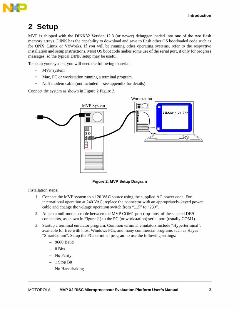
2 SetupMVP is shipped with the DINK32 Version 12.3 (or newer) debugger loaded into one of the two flashmemory arrays. DINK has the capability to download and save to flash other OS bootloaded code such asfor QNX, Linux or VxWorks. If you will be running other operating systems, refer to the respectiveinstallation and setup instructions. Most OS boot code makes some use of the serial port, if only for progressmessages, so the typical DINK setup may be useful.
To setup your system, you will need the following material:
• MVP system
• Mac, PC or workstation running a terminal program.
• Null-modem cable (not included -- see appendix for details).
Connect the system as shown in Figure 2.Figure 2.
Figure 2. MVP Setup Diagram
Installation steps:
1. Connect the MVP system to a 120 VAC source using the supplied AC power code. For international operation at 240 VAC, replace the connector with an appropriately-keyed power cable and change the voltage operation switch from “115” to “230”.
2. Attach a null-modem cable between the MVP COM1 port (top-most of the stacked DB9 connectors, as shown in Figure 2.) to the PC (or workstation) serial port (usually COM1).
3. Startup a terminal emulator program. Common terminal emulators include “Hyperterminal”, available for free with most Windows PCs, and many commercial programs such as Hayes “SmartComm”. Setup the PCs terminal program to use the following settings:
– 9600 Baud
– 8 Bits
– No Parity
– 1 Stop Bit
– No Handshaking
1
CO
M2
1
COM
1CO
M2
',1.��!!�JR����
CO
M1
Workstation
MVP System
MOTOROLA MVP X2 RISC Microprocessor Evaluation Platform User’s Manual 3
Introduction
– Terminal Emulation: any
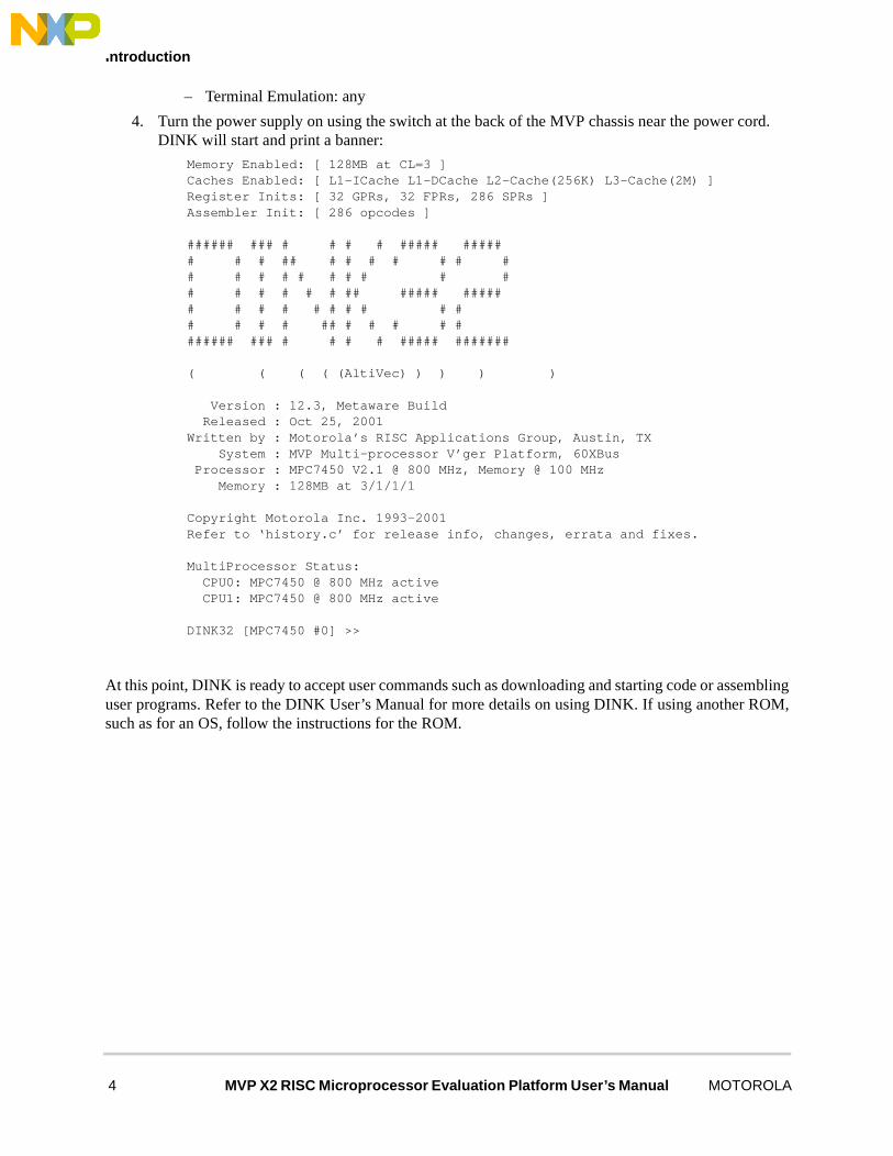
4. Turn the power supply on using the switch at the back of the MVP chassis near the power cord. DINK will start and print a banner:
Memory Enabled: [ 128MB at CL=3 ]Caches Enabled: [ L1-ICache L1-DCache L2-Cache(256K) L3-Cache(2M) ]Register Inits: [ 32 GPRs, 32 FPRs, 286 SPRs ]Assembler Init: [ 286 opcodes ]
###### ### # # # # ##### ###### # # ## # # # # # # ## # # # # # # # # ## # # # # # ## ##### ###### # # # # # # # # ## # # # ## # # # # ####### ### # # # # ##### #######
( ( ( ( (AltiVec) ) ) ) )
Version : 12.3, Metaware BuildReleased : Oct 25, 2001
Written by : Motorola’s RISC Applications Group, Austin, TXSystem : MVP Multi-processor V’ger Platform, 60XBus
Processor : MPC7450 V2.1 @ 800 MHz, Memory @ 100 MHz Memory : 128MB at 3/1/1/1
Copyright Motorola Inc. 1993-2001Refer to ‘history.c’ for release info, changes, errata and fixes.
MultiProcessor Status:CPU0: MPC7450 @ 800 MHz activeCPU1: MPC7450 @ 800 MHz active
DINK32 [MPC7450 #0] >>
At this point, DINK is ready to accept user commands such as downloading and starting code or assemblinguser programs. Refer to the DINK User’s Manual for more details on using DINK. If using another ROM,such as for an OS, follow the instructions for the ROM.
4 MVP X2 RISC Microprocessor Evaluation Platform User’s Manual MOTOROLA

Introduction
3 ConfigurationMVP is shipped ready to run the DINK firmware by default. Memory and cache configuration is set by theDINK software (see the DINK user’s manual for details). Other options, such as system bus frequency areset with switches on the MVP motherboard.
To re-configure the system, remove the AC cord and open the chassis cover by removing the fourPhilips-head screws from the back of the chassis, exposing the motherboard.
It may be easier to reconfigure the system by also removing the two screws holding the slide-in motherboardframe to the chassis. If desired, slide it out partially so the front-panel switches are not disconnected.
All options on MVP are set via four 8-position ‘DIP’ switches, as shown in Figure 3.
Figure 3. MVP in an ATX Chassis
The switches have the same orientation; with the system standing vertically, the switches operate as shownwhere “ON” is to the left and “OFF” is to the right.
All configuration switches should be changed with the power off; most changes only take effect on a systempower-on reset. The system pushbutton reset is not necessarily sufficient.
Table 1. MVP Configuration Switches
Switch No OptionDefault Setting
Description
SW7 1:8 Clock Code See Section 3.1
POWERSUPPLY
GT64260
SW6
SW7
�
�
�
�
�
�
�
�
21
LEFT = ON
RIGHT = OFF
�
�
�
�
�
�
�
�
21
�
�
�
�
�
�
�
�
21
�
�
�
�
�
�
�
�
21
�
�
�
�
�
�
�
�
21
SW5
SW4
MOTOROLA MVP X2 RISC Microprocessor Evaluation Platform User’s Manual 5
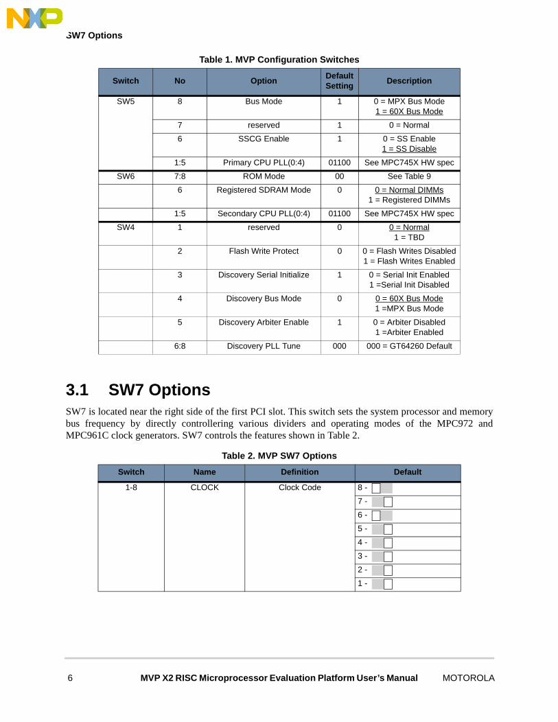
SW7 Options
3.1 SW7 OptionsSW7 is located near the right side of the first PCI slot. This switch sets the system processor and memorybus frequency by directly controllering various dividers and operating modes of the MPC972 andMPC961C clock generators. SW7 controls the features shown in Table 2.
SW5 8 Bus Mode 1 0 = MPX Bus Mode1 = 60X Bus Mode
7 reserved 1 0 = Normal
6 SSCG Enable 1 0 = SS Enable1 = SS Disable
1:5 Primary CPU PLL(0:4) 01100 See MPC745X HW spec
SW6 7:8 ROM Mode 00 See Table 9
6 Registered SDRAM Mode 0 0 = Normal DIMMs1 = Registered DIMMs
1:5 Secondary CPU PLL(0:4) 01100 See MPC745X HW spec
SW4 1 reserved 0 0 = Normal1 = TBD
2 Flash Write Protect 0 0 = Flash Writes Disabled1 = Flash Writes Enabled
3 Discovery Serial Initialize 1 0 = Serial Init Enabled1 =Serial Init Disabled
4 Discovery Bus Mode 0 0 = 60X Bus Mode1 =MPX Bus Mode
5 Discovery Arbiter Enable 1 0 = Arbiter Disabled1 =Arbiter Enabled
6:8 Discovery PLL Tune 000 000 = GT64260 Default
Table 2. MVP SW7 Options
Switch Name Definition Default
1-8 CLOCK Clock Code 8 -
7 -
6 -
5 -
4 -
3 -
2 -
1 -
Table 1. MVP Configuration Switches
Switch No OptionDefault Setting
Description
6 MVP X2 RISC Microprocessor Evaluation Platform User’s Manual MOTOROLA
SW5 Options
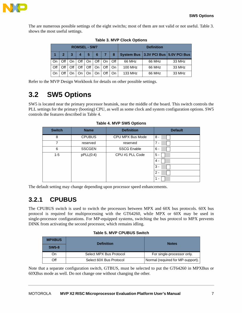
The are numerous possible settings of the eight switchs; most of them are not valid or not useful. Table 3.shows the most useful settings.
Refer to the MVP Design Workbook for details on other possible settings.
3.2 SW5 OptionsSW5 is located near the primary processor heatsink, near the middle of the board. This switch controls thePLL settings for the primary (booting) CPU, as well as some clock and system configuration options. SW5controls the features described in Table 4.
The default setting may change depending upon processor speed enhancements.
3.2.1 CPUBUSThe CPUBUS switch is used to switch the processors between MPX and 60X bus protocols. 60X busprotocol is required for multiprocessing with the GT64260, while MPX or 60X may be used insingle-processor configurations. For MP-equipped systems, switching the bus protocol to MPX preventsDINK from activating the second processor, which remains idling.
Note that a separate configuration switch, GTBUS, must be selected to put the GT64260 in MPXBus or60XBus mode as well. Do not change one without changing the other.
Table 3. MVP Clock Options
ROMSEL - SW7 Definition
1 2 3 4 5 6 7 8 System Bus 3.3V PCI Bus 5.0V PCI Bus
On Off On Off On Off On Off 66 MHz 66 MHz 33 MHz
Off Off Off Off Off On Off On 100 MHz 66 MHz 33 MHz
On Off On On On On Off On 133 MHz 66 MHz 33 MHz
Table 4. MVP SW5 Options
Switch Name Definition Default
8 CPUBUS CPU MPX Bus Mode 8 -
7 reserved reserved 7 -
6 SSCGEN SSCG Enable 6 -
1-5 pPLL(0:4) CPU #1 PLL Code 5 -
4 -
3 -
2 -
1 -
Table 5. MVP CPUBUS Switch
MPXBUSDefinition Notes
SW5-8
On Select MPX Bus Protocol For single-processor only.
Off Select 60X Bus Protocol Normal (required for MP-support).
MOTOROLA MVP X2 RISC Microprocessor Evaluation Platform User’s Manual 7
SW6 Options
3.2.2 SSCGENThe SSCGEN switch is used to enable the spread-spectrum modulation of the clock generator.
The SSCG option is for test purposes only. It modulates the system clock downward -1.25%. While thesystem is expected to operate fully, there is a slight decrease in performance due to the slowed clock.
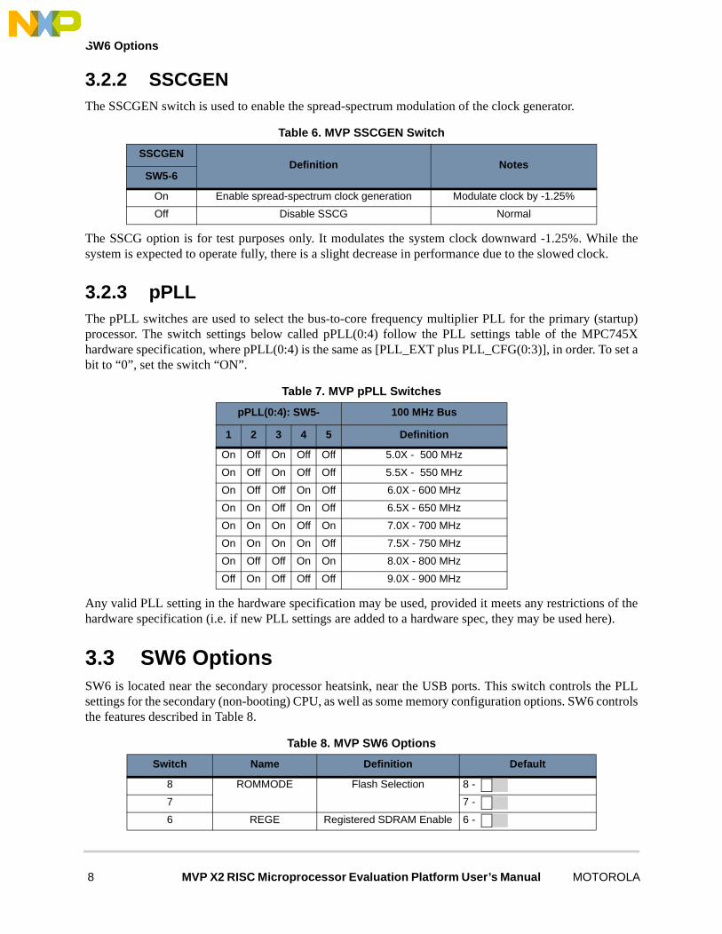
3.2.3 pPLLThe pPLL switches are used to select the bus-to-core frequency multiplier PLL for the primary (startup)processor. The switch settings below called pPLL(0:4) follow the PLL settings table of the MPC745Xhardware specification, where pPLL(0:4) is the same as [PLL_EXT plus PLL_CFG(0:3)], in order. To set abit to “0”, set the switch “ON”.
Any valid PLL setting in the hardware specification may be used, provided it meets any restrictions of thehardware specification (i.e. if new PLL settings are added to a hardware spec, they may be used here).
3.3 SW6 OptionsSW6 is located near the secondary processor heatsink, near the USB ports. This switch controls the PLLsettings for the secondary (non-booting) CPU, as well as some memory configuration options. SW6 controlsthe features described in Table 8.
Table 6. MVP SSCGEN Switch
SSCGENDefinition Notes
SW5-6
On Enable spread-spectrum clock generation Modulate clock by -1.25%
Off Disable SSCG Normal
Table 7. MVP pPLL Switches
pPLL(0:4): SW5- 100 MHz Bus
1 2 3 4 5 Definition
On Off On Off Off 5.0X - 500 MHz
On Off On Off Off 5.5X - 550 MHz
On Off Off On Off 6.0X - 600 MHz
On On Off On Off 6.5X - 650 MHz
On On On Off On 7.0X - 700 MHz
On On On On Off 7.5X - 750 MHz
On Off Off On On 8.0X - 800 MHz
Off On Off Off Off 9.0X - 900 MHz
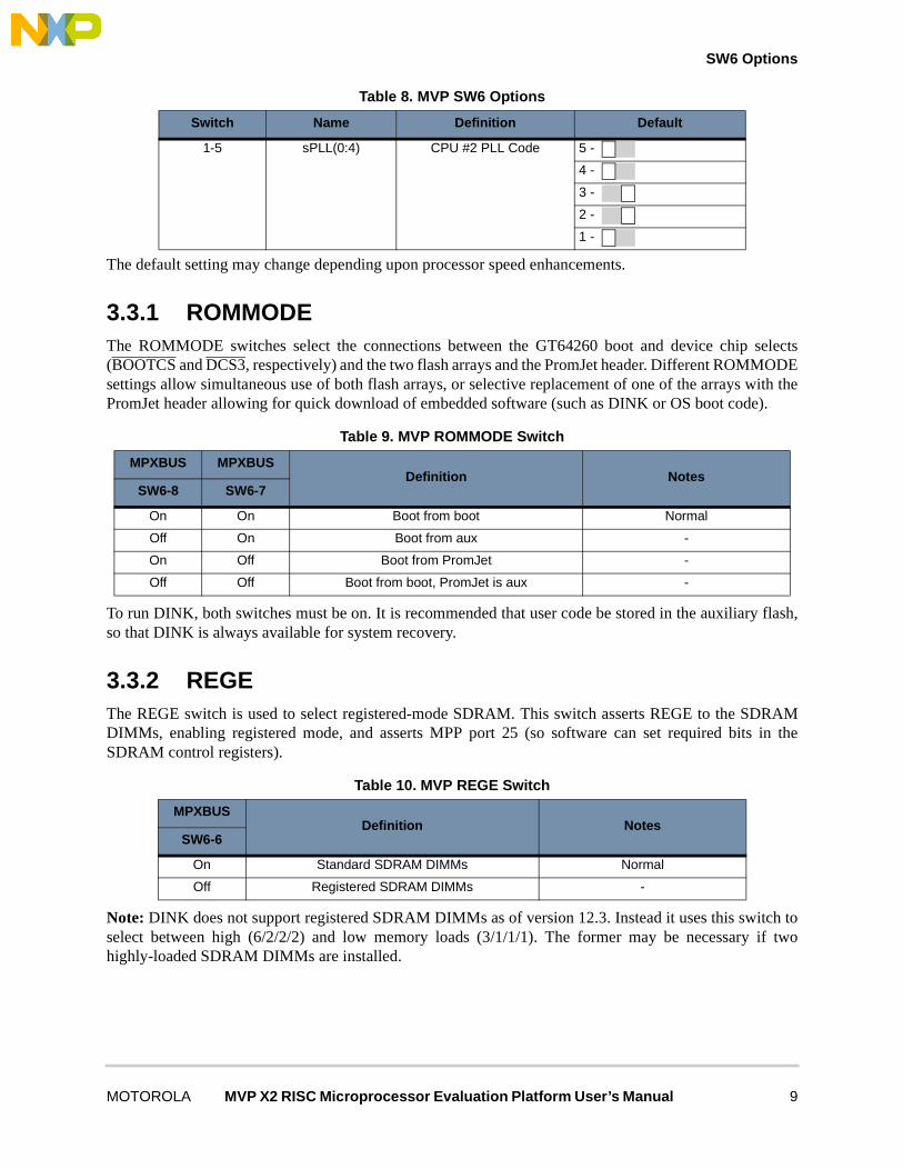
Table 8. MVP SW6 Options
Switch Name Definition Default
8 ROMMODE Flash Selection 8 -
7 7 -
6 REGE Registered SDRAM Enable 6 -
8 MVP X2 RISC Microprocessor Evaluation Platform User’s Manual MOTOROLA
SW6 Options
The default setting may change depending upon processor speed enhancements.
3.3.1 ROMMODEThe ROMMODE switches select the connections between the GT64260 boot and device chip selects(BOOTCS and DCS3, respectively) and the two flash arrays and the PromJet header. Different ROMMODEsettings allow simultaneous use of both flash arrays, or selective replacement of one of the arrays with thePromJet header allowing for quick download of embedded software (such as DINK or OS boot code).
To run DINK, both switches must be on. It is recommended that user code be stored in the auxiliary flash,so that DINK is always available for system recovery.
3.3.2 REGEThe REGE switch is used to select registered-mode SDRAM. This switch asserts REGE to the SDRAMDIMMs, enabling registered mode, and asserts MPP port 25 (so software can set required bits in theSDRAM control registers).
Note: DINK does not support registered SDRAM DIMMs as of version 12.3. Instead it uses this switch toselect between high (6/2/2/2) and low memory loads (3/1/1/1). The former may be necessary if twohighly-loaded SDRAM DIMMs are installed.
1-5 sPLL(0:4) CPU #2 PLL Code 5 -
4 -
3 -
2 -
1 -
Table 9. MVP ROMMODE Switch
MPXBUS MPXBUSDefinition Notes
SW6-8 SW6-7
On On Boot from boot Normal
Off On Boot from aux -
On Off Boot from PromJet -
Off Off Boot from boot, PromJet is aux -
Table 10. MVP REGE Switch
MPXBUSDefinition Notes
SW6-6
On Standard SDRAM DIMMs Normal
Off Registered SDRAM DIMMs -
Table 8. MVP SW6 Options
Switch Name Definition Default
MOTOROLA MVP X2 RISC Microprocessor Evaluation Platform User’s Manual 9
SW4 Options
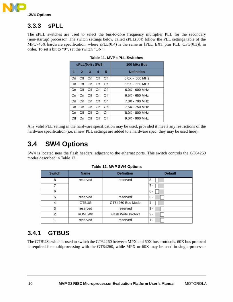
3.3.3 sPLLThe sPLL switches are used to select the bus-to-core frequency multiplier PLL for the secondary(non-startup) processor. The switch settings below called sPLL(0:4) follow the PLL settings table of theMPC745X hardware specification, where sPLL(0:4) is the same as [PLL_EXT plus PLL_CFG(0:3)], inorder. To set a bit to “0”, set the switch “ON”.
Any valid PLL setting in the hardware specification may be used, provided it meets any restrictions of thehardware specification (i.e. if new PLL settings are added to a hardware spec, they may be used here).
3.4 SW4 OptionsSW4 is located near the flash headers, adjacent to the ethernet ports. This switch controls the GT64260modes described in Table 12.
3.4.1 GTBUSThe GTBUS switch is used to switch the GT64260 between MPX and 60X bus protocols. 60X bus protocolis required for multiprocessing with the GT64260, while MPX or 60X may be used in single-processor
Table 11. MVP sPLL Switches
sPLL(0:4) : SW6- 100 MHz Bus
1 2 3 4 5 Definition
On Off On Off Off 5.0X - 500 MHz
On Off On Off Off 5.5X - 550 MHz
On Off Off On Off 6.0X - 600 MHz
On On Off On Off 6.5X - 650 MHz
On On On Off On 7.0X - 700 MHz
On On On On Off 7.5X - 750 MHz
On Off Off On On 8.0X - 800 MHz
Off On Off Off Off 9.0X - 900 MHz
Table 12. MVP SW4 Options
Switch Name Definition Default
8 reserved reserved 8 -
7 7 -
6 6 -
5 reserved reserved 5 -
4 GTBUS GT64260 Bus Mode 4 -
3 reserved reserved 3 -
2 ROM_WP Flash Write Protect 2 -
1 reserved reserved 1 -
10 MVP X2 RISC Microprocessor Evaluation Platform User’s Manual MOTOROLA

SW4 Options
configurations. For MP-equipped systems, switching the bus protocol to MPX prevents DINK fromactivating the second processor, which remains idling.
Note that a separate configuration switch, CPUBUS, must be selected to put the processor in MPXBus or60XBus mode as well. Do not change one without changing the other.
Note that GTBUS is the opposite sense of CPUBUS, so the two switches should always be set oppositely.
3.4.2 ROM_WPThe ROM_WP switch is used to write-protect the local flash devices. If set, writes to the devices will beignored..
Note that if flash is write-protected, the DINK flash programming algorithm cannot detect the flash devicetype, so it will produce erroneous errors.
Table 13. MVP GTBUS Switch
MPXBUSDefinition Notes
SW4-4
On Select 60X Bus Protocol Normal (required for MP-support).
Off Select MPX Bus Protocol For single-processor only.
Table 14. MVP ROM_WP Switch
MPXBUSDefinition Notes
SW4-2
On Flash is write-protected. -
Off Flash may be written to. Normal
MOTOROLA MVP X2 RISC Microprocessor Evaluation Platform User’s Manual 11

Address Map
4 Programmers ModelThis section describes support information which may be useful to hardware or software designers who areusing MVP.
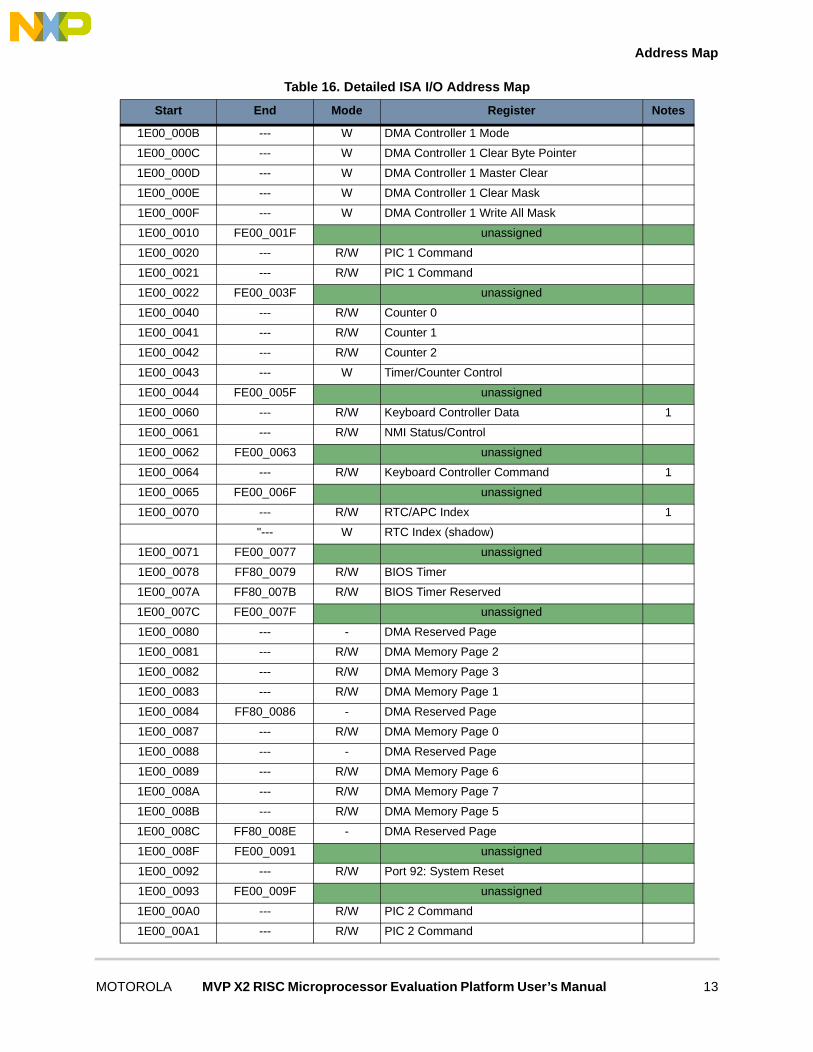
4.1 Address MapTable 15.shows the general address map of the MVP, and Table 15 shows the specific location of ISA/PCII/O addresses.
NOTES:1. Optional, obsolete GT64260 register space.2. Used by DINK; requires programming of GT64260 registers.3. Default GT64260 register space.
The detailed address map in Table 16 assumes that the PnP devices have not been changed from the defaultlocations.
Table 15. Global Address Map
START END Definition Notes
0000_0000 13FF_FFFF SDRAM
1400_0000 14FF_FFFF GT64260 registers 1
1500_0000 1DFF_FFFF SDRAM
1E00_0000 1EFF_FFFF sPCI IO space 2
1F00_0000 1FFF_FFFF SDRAM
2000_0000 F0FF_FFFF unused
F100_0000 F1FF_FFFF GT64260 registers 3
F200_0000 FDFF_FFFF unused
FE00_0000 FEFF_FFFF Alternate flash space
FF00_0000 FFFF_FFFF Boot flash space
Table 16. Detailed ISA I/O Address Map
Start End Mode Register Notes
1E00_0000 --- R/W DMA Channel 0 Base/Current Address
1E00_0001 --- R/W DMA Channel 0 Base/Current Word
1E00_0002 --- R/W DMA Channel 1 Base/Current Address
1E00_0003 --- R/W DMA Channel 1 Base/Current Word
1E00_0004 --- R/W DMA Channel 2 Base/Current Address
1E00_0005 --- R/W DMA Channel 2 Base/Current Word
1E00_0006 --- R/W DMA Channel 3 Base/Current Address
1E00_0007 --- R/W DMA Channel 3 Base/Current Word
1E00_0008 --- R DMA Controller 1 Status
W DMA Controller 1 Command
1E00_0009 --- W DMA Controller 1 Request
1E00_000A --- W DMA Controller 1 Mask
12 MVP X2 RISC Microprocessor Evaluation Platform User’s Manual MOTOROLA
Address Map
1E00_000B --- W DMA Controller 1 Mode
1E00_000C --- W DMA Controller 1 Clear Byte Pointer
1E00_000D --- W DMA Controller 1 Master Clear
1E00_000E --- W DMA Controller 1 Clear Mask
1E00_000F --- W DMA Controller 1 Write All Mask
1E00_0010 FE00_001F unassigned
1E00_0020 --- R/W PIC 1 Command
1E00_0021 --- R/W PIC 1 Command
1E00_0022 FE00_003F unassigned
1E00_0040 --- R/W Counter 0
1E00_0041 --- R/W Counter 1
1E00_0042 --- R/W Counter 2
1E00_0043 --- W Timer/Counter Control
1E00_0044 FE00_005F unassigned
1E00_0060 --- R/W Keyboard Controller Data 1
1E00_0061 --- R/W NMI Status/Control
1E00_0062 FE00_0063 unassigned
1E00_0064 --- R/W Keyboard Controller Command 1
1E00_0065 FE00_006F unassigned
1E00_0070 --- R/W RTC/APC Index 1
"--- W RTC Index (shadow)
1E00_0071 FE00_0077 unassigned
1E00_0078 FF80_0079 R/W BIOS Timer
1E00_007A FF80_007B R/W BIOS Timer Reserved
1E00_007C FE00_007F unassigned
1E00_0080 --- - DMA Reserved Page
1E00_0081 --- R/W DMA Memory Page 2
1E00_0082 --- R/W DMA Memory Page 3
1E00_0083 --- R/W DMA Memory Page 1
1E00_0084 FF80_0086 - DMA Reserved Page
1E00_0087 --- R/W DMA Memory Page 0
1E00_0088 --- - DMA Reserved Page
1E00_0089 --- R/W DMA Memory Page 6
1E00_008A --- R/W DMA Memory Page 7
1E00_008B --- R/W DMA Memory Page 5
1E00_008C FF80_008E - DMA Reserved Page
1E00_008F FE00_0091 unassigned
1E00_0092 --- R/W Port 92: System Reset
1E00_0093 FE00_009F unassigned
1E00_00A0 --- R/W PIC 2 Command
1E00_00A1 --- R/W PIC 2 Command
Table 16. Detailed ISA I/O Address Map
Start End Mode Register Notes
MOTOROLA MVP X2 RISC Microprocessor Evaluation Platform User’s Manual 13

Address Map
1E00_00A2 FE00_00BF unassigned
1E00_00C0 --- R/W DMA Channel 4 Base/Current Address
1E00_00C1 --- R/W DMA Channel 4 Base/Current Word
1E00_00C2 FE00_00C3 unassigned
1E00_00C4 --- R/W DMA Channel 5 Base/Current Address
1E00_00C5 unassigned
1E00_00C6 --- R/W DMA Channel 5 Base/Current Word
1E00_00C7 unassigned
1E00_00C8 --- R/W DMA Channel 6 Base/Current Address
1E00_00C9 unassigned
1E00_00CA --- R/W DMA Channel 6 Base/Current Word
1E00_00CB unassigned
1E00_00CC --- R/W DMA Channel 7 Base/Current Address
1E00_00CD unassigned
1E00_00CE --- R/W DMA Channel 7 Base/Current Word
1E00_00CF unassigned
1E00_00D0 R DMA Controller 2 Status
"W DMA Controller 2 Command
1E00_00D3 unassigned
1E00_00D2 --- W DMA Controller 2 Request
1E00_00D3 unassigned
1E00_00D4 --- W DMA Controller 2 Mask
1E00_00D5 unassigned
1E00_00D6 --- W DMA Controller 2 Mode W
1E00_00D7 unassigned
1E00_00D8 --- W DMA Controller 2 Clear Byte Pointer
1E00_00D9 unassigned
1E00_00DA --- W DMA Controller 2 Master Clear
1E00_00DB unassigned
1E00_00DC --- W DMA Controller 2 Clear Mask
1E00_00DD unassigned
1E00_00DE --- W DMA Controller 2 Write All Mask
1E00_00DF FE00_00EF unassigned
1E00_00F0 --- W Coprocessor Error
1E00_00F1 FE00_016F unassigned
1E00_0170 FE00_0177 R/W IDE Channel 2 Primary
1E00_0178 FE00_01EF unassigned
1E00_01F0 FE00_01F7 R/W IDE Channel 1 Primary
1E00_01F8 FE00_0375 unassigned
1E00_0376 --- R/W IDE Channel 2 Secondary
1E00_0377 FE00_03F5 unassigned
Table 16. Detailed ISA I/O Address Map
Start End Mode Register Notes
14 MVP X2 RISC Microprocessor Evaluation Platform User’s Manual MOTOROLA

Address Map
1E00_03F6 --- R/W IDE Channel 1 Secondary
1E00_03F7 FE00_0409 unassigned
1E00_040A --- R DMA Scatter/Gather Interrupt Status
1E00_040B --- W DMA Controller 1 Extended Mode
1E00_040C FE00_0414 unassigned
1E00_0415 --- W DMA Scatter/Gather Channel 5 Command
1E00_0416 --- W DMA Scatter/Gather Channel 6 Command
1E00_0417 --- W DMA Scatter/Gather Channel 7 Command
1E00_0418 FE00_041C unassigned
1E00_041D --- R DMA Scatter/Gather Channel 5 Status
1E00_041E --- R DMA Scatter/Gather Channel 6 Status
1E00_041F --- R DMA Scatter/Gather Channel 7 Status
1E00_0420 FE00_0433 unassigned
1E00_0434 FE00_0437 R/W DMA Scatter/Gather Channel 5 Table Pointer
1E00_0438 FE00_043B R/W DMA Scatter/Gather Channel 6 Table Pointer
1E00_043C FE00_043F R/W DMA Scatter/Gather Channel 7 Table Pointer
1E00_0440 FE00_0480 unassigned
1E00_0481 --- R/W DMA Page Register 2
1E00_0482 --- R/W DMA Page Register 3
1E00_0483 --- R/W DMA Page Register 1
1E00_0484 FE00_0486 unassigned
1E00_0487 --- R/W DMA Page Register 0
1E00_0488 unassigned
1E00_0489 --- R/W DMA Page Register 6
1E00_048A --- R/W DMA Page Register 7
1E00_048B --- R/W DMA Page Register 5
1E00_048C FE00_04CF unassigned
1E00_04D0 --- R/W PIC 1 Interrupt Control
1E00_04D1 --- R/W PIC 2 Interrupt Control
1E00_04D2 FE00_080F unassigned
1E00_0810 --- W RTC CMOS RAM Protect 1
1E00_0812 --- W RTC CMOS RAM Protect 2
1E00_0813 FEBF_FFFF unassigned
Table 16. Detailed ISA I/O Address Map
Start End Mode Register Notes
MOTOROLA MVP X2 RISC Microprocessor Evaluation Platform User’s Manual 15
Code Development
5 Development IssuesThe following sections cover a few issues related to developing software on the MVP platform.
5.1 Code DevelopmentSoftware can generally be developed on a Unix workstation or PC and downloaded to the MVP using theDINK serial S-record download facility, third-party COP controllers, or the PromJetTM device.
Refer to:
http://e-www.motorola.com/webapp/sps/design_tools/index_dt.jsp
for further details. There are several ways of doing this, depending on the resources available.
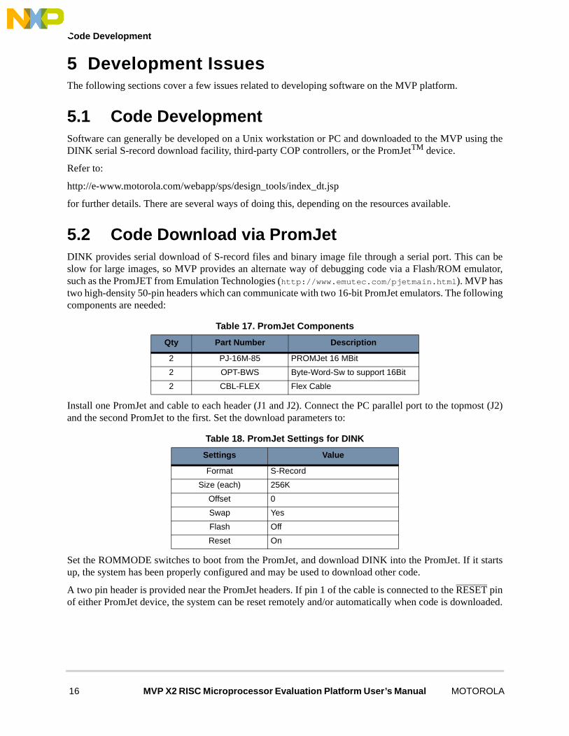
5.2 Code Download via PromJetDINK provides serial download of S-record files and binary image file through a serial port. This can beslow for large images, so MVP provides an alternate way of debugging code via a Flash/ROM emulator,such as the PromJET from Emulation Technologies (http://www.emutec.com/pjetmain.html). MVP hastwo high-density 50-pin headers which can communicate with two 16-bit PromJet emulators. The followingcomponents are needed:
Install one PromJet and cable to each header (J1 and J2). Connect the PC parallel port to the topmost (J2)and the second PromJet to the first. Set the download parameters to:
Set the ROMMODE switches to boot from the PromJet, and download DINK into the PromJet. If it startsup, the system has been properly configured and may be used to download other code.
A two pin header is provided near the PromJet headers. If pin 1 of the cable is connected to the RESET pinof either PromJet device, the system can be reset remotely and/or automatically when code is downloaded.
Table 17. PromJet Components
Qty Part Number Description
2 PJ-16M-85 PROMJet 16 MBit
2 OPT-BWS Byte-Word-Sw to support 16Bit
2 CBL-FLEX Flex Cable
Table 18. PromJet Settings for DINK
Settings Value
Format S-Record
Size (each) 256K
Offset 0
Swap Yes
Flash Off
Reset On
16 MVP X2 RISC Microprocessor Evaluation Platform User’s Manual MOTOROLA

User Code in Flash
5.2.1 PromJet OffsetsThe PromJet has the capability of limiting the apparent size of the PromJet. This can speed up downloadsand more accurately reflect the target system, but makes offset setting tricky. In the previous section, thePromJets were set to 256K, for a total of 512K. Why was the offset ‘0’? Because the image is ‘replicated’when smaller than the target size. Code at 0xFFF0_0100 is also found at
Had the size been set to 512K, code would not have been replicated, but since it is 512K from the top, thevectors would be placed at 0xFFE0_0100 -- incorrect. So if the size were set to 512K, offset must be set to0x10_0000. Then DINK would reside at 0xFFF0_0000-0xFFFF_FFFF and the area from0xFFE0_0000-0xFEFF_FFFF would be available for user code.
In a similar manner, a size of 1M would require an offset of 0x30_0000 to get the vectors in the properposition (note that the changes are all powers-of-two, or masks thereof).
Each “block” in the above table represents a copies of the same downloaded image. Only the “8M” settingfills the entire space (2 x 8M = 16MB, the space allocated for each flash array and corresponding to the twoAm29LV641 64MBit/8MB flash devices used on MVP).
5.3 User Code in FlashDINK has the capability of saving user code to the flash. Generally, user code is written to the auxiliary flasharray. The main flash array contains DINK and can be overwritten; however, if DINK is not present it maybe difficult to recover and will make it difficult for you to get support from the RISC Applications group.
To save an image to the auxiliary flash:
Table 19. PromJet Offsets
Address Size = 256K Size = 512K Size = 1M Size = 2M Size = 4M Size = 8M
FFF8_0000
FFF0_0000
FFE8_0000
FFE0_0000
FFD8_0000
FFD0_0000
FFC8_0000
FFC0_0000
FFB8_0000
FFB0_0000
FFA8_0000
FFA0_0000
FF98_0000
FF90_0000
FF88_0000
FF80_0000
...
MOTOROLA MVP X2 RISC Microprocessor Evaluation Platform User’s Manual 17

Saving Bootable Images to Flash
1. Issue the command:fu -l <src_addr> fef00000 100000
where “src_addr” is the address of your code, which could be an SDRAM address (e.g. “100000”) where code was downloaded as an S-record, or a flash address (e.g. “fff00000”) which contains code (possibly in an PromJet device).
2. If you want to boot your code through DINK (i.e. DINK initializes the system, enter the following:“ENV BOOT=0xFEF00000”
or whatever is the correct entry address for your program.
5.4 Saving Bootable Images to FlashWhile the above procedure saves data to flash, two additional factors must be considered if the goal is tohave the system boot the code immediately after reset. Motorola implementations of the PowerPCarchitecture begin executing code at 0xFFF0_0100, so valid reset vector .
If the compiler/linker places the exception vectors at the start of the code image, as is the case with DINK,then the code must be in memory starting at 0xFFF0_0100. When programming to the auxiliary space andthen swapping flash banks, the equivalent address is 0xFEF0_0100.
Since the top of memory is at 0xFFFF_FFFF, a code image produced this way cannot be larger than 1MB.
To write larger images, the vectors must in the proper position such that the reset vector code ends up at0xFFF00100. For example, a 2MB program could be ‘flashed’ at address 0xFFE0_0000 or 0xFEE0_0000(depending on how you do it), and this program must be linked such that the vectors start 1MB within theimage.
Most linkers are capable of positioning special sections at dedicated addresses. Each linker is a littledifferent, so consult the compiler vendor for details.
The second issue to consider is that DINK performs a great deal of setup; if you have developed code andrun it through DINK, you might not have all needed system initialization. For independant bootable images,you will have to provide the proper system initialization code.
5.5 Upgrading DINKOccasionally, DINK is upgraded with new facilities and bug fixes. DINK has the ability to update itselfusing the “fupdate” command. To update DINK with a new version, follow this sequence:
Table 20. Aliased Flash Addresses
Address as Main Flash Address as Aux. Flash Size
0xFFF0_0000 0xFEF0_0000 1MB Boot vectors must be loaded here!
0xFFE0_0000 0xFEE0_0000 1MB
0xFFD0_0000 0xFED0_0000 1MB
0xFFC0_0000 0xFEC0_0000 1MB
0xFFB0_0000 0xFEB0_0000 1MB
... ...
0xFF10_0000 0xFE10_0000 1MB
0xFF00_0000 0xFE00_0000 1MB Bottom of flash areas.
18 MVP X2 RISC Microprocessor Evaluation Platform User’s Manual MOTOROLA
Upgrading DINK
1. Obtain the S-record or binary image of the DINK upgrade. Be sure to select the MVP version, as versions for Sandpoint or Excimer will not run. DINK images are available in the “Design Tools” section of the Motorola 32-bit embedded processors webpage.
2. Consider writing DINK to the auxiliary flash so that in the event of an error the previous version of DINK will be available. If DINK is erased there is no way to restore it other than with an external PromJet header or through a COP controller.
3. Download the S-record file to the Sandpoint platform using the command:dl -k -o 100000
with the terminal program, in the usual manner. You can also convert it to binary for faster download, as described in the DINK manual).
4. Issue the command:fu -h 100000 fff00000 7ff00
if writing to the standard flash bank, andfu -h 100000 fef00000 7ff00
if writing to the auxiliary flash bank.
Restart, and the new version of DINK should activate (switch to the auxiliary bank if needed).
MOTOROLA MVP X2 RISC Microprocessor Evaluation Platform User’s Manual 19

Null Modem Cable
6 Other Information
6.1 Null Modem CableDINK requires only a simple null-modem cable, with no flow control. Figure 4 shows a simple example.
Figure 4. Null Modem Diagram
6.2 Reference DocumentationTable 21 describes reference documentation which may be useful for understanding the operation of theSandpoint or an attached MPPMC card:
Table 21. Reference Documentation
Document Number/Reference
Sandpoint 3 Technical SummarySchematicsErrata
http://www.mot.com/SPS/PowerPC/teksupport/refdesigns/sandpoint.html
MPPMC SchematicsDocumentationErrata
http://www.mot.com/SPS/PowerPC/teksupport/refdesigns/sandpoint.html
MPC8240 User’s Manual http://e-www.motorola.com/brdata/PDFDB/MICROPROCESSORS/32_BIT/POWERPC/MPC82XX/MPC8240UM.pdf
MPC107 User’s Manual http://e-www.motorola.com/brdata/PDFDB/MICROPROCESSORS/32_BIT/POWERPC/MPC1XX/MPC107UM.pdf
DINK User’s Manualand code updates
http://www.mot.com/SPS/PowerPC/teksupport/tools/DINK32/dinkindex.htm
Draft Standard Physical and Environmental Layers for Processor PCI Mezzanine Cards: PrPMC
http://www.vita.com/vso/
PCI 2.1 Specification http://www.pcisig.com
Draft Standard Physical and Environmental Layers for PCI Mezzanine Cards: PMC
IEEE P1386.1/Draft 2.0 04-APR-1995
DB9 FemaleBack View
1
59
62
3
48
7
DB9 FemaleBack View
1
59
62
3
48
7
20 MVP X2 RISC Microprocessor Evaluation Platform User’s Manual MOTOROLA

Glossary
6.3 GlossaryTable 22 explains some terminology used in this document:
Draft Standard for a Common Mezzanine Card Family: CMC IEEE P1386/Draft 2.0 04-APR-1995
Winbond W83C553 Datasheet http://www.winbond.com.tw/sheet/w83c553f.pdforhttp:///www.winbond.com.tw/
National Semi. PC87307/97307 Datasheet http://www.national.com/pf/PC/PC97307.htmlorhttp:///www.national.com/design/
Table 22. Terminology
Term Definition
ATA AT (PC format) Attach - protocol for communicating over IDE bus.
ATX Form factor for chassis.
BBRAM Battery-Backed Random Access Memory
IDE Integrated Device Electronics -- common disk interface signalling.
MPPMC Motorola Processor PCI Mezzanine Card -- an superset of the VITA PrPMC specification proposal which adds PCI arbitration.
PCI Peripheral Connect Interface
PMC PCI Mezzanine Card -- a small form-factor PCI-2.0 compliant daughtercard standard.
PPMC Processor PCI Mezzanine Card -- an early name for PrPMC; no longer used.
PrPMC Processor PCI Mezzanine Card -- an extension to the IEEE1386 PMC standard adding host-related functions and PCI-2.1 compatibility (was formerly called PPMC).
RAM Are you kidding?
RTC Real Time Clock
SIO System I/O (or SuperIO) - National Semi. PC-I/O device.
WB WinBond, manufacturer of the ISA/IDE interface.
Table 21. Reference Documentation
Document Number/Reference
MOTOROLA MVP X2 RISC Microprocessor Evaluation Platform User’s Manual 21
MVPX2UM/D
HOW TO REACH US:
USA/EUROPE/LOCATIONS NOT LISTED:
Motorola Literature Distribution; P.O. Box 5405, Denver, Colorado 80217 1-303-675-2140 or 1-800-441-2447
JAPAN:
Motorola Japan Ltd.; SPS, Technical Information Center, 3-20-1, Minami-Azabu Minato-ku, Tokyo 106-8573 Japan81-3-3440-3569
ASIA/PACIFIC:
Motorola Semiconductors H.K. Ltd.; Silicon Harbour Centre, 2 Dai King Street, Tai Po Industrial Estate, Tai Po, N.T., Hong Kong852-26668334
TECHNICAL INFORMATION CENTER:
1-800-521-6274
HOME PAGE:
http://www.motorola.com/semiconductors
DOCUMENT COMMENTS:
FAX (512) 933-2625, Attn: RISC Applications Engineering
Information in this document is provided solely to enable system and software implementers to use
Motorola products. There are no express or implied copyright licenses granted hereunder to design or
fabricate any integrated circuits or integrated circuits based on the information in this document.
Motorola reserves the right to make changes without further notice to any products herein. Motorola
makes no warranty, representation or guarantee regarding the suitability of its products for any
particular purpose, nor does Motorola assume any liability arising out of the application or use of any
product or circuit, and specifically disclaims any and all liability, including without limitation
consequential or incidental damages. “Typical” parameters which may be provided in Motorola data
sheets and/or specifications can and do vary in different applications and actual performance may vary
over time. All operating parameters, including “Typicals” must be validated for each customer
application by customer’s technical experts. Motorola does not convey any license under its patent
rights nor the rights of others. Motorola products are not designed, intended, or authorized for use as
components in systems intended for surgical implant into the body, or other applications intended to
support or sustain life, or for any other application in which the failure of the Motorola product could
create a situation where personal injury or death may occur. Should Buyer purchase or use Motorola
products for any such unintended or unauthorized application, Buyer shall indemnify and hold
Motorola and its officers, employees, subsidiaries, affiliates, and distributors harmless against all
claims, costs, damages, and expenses, and reasonable attorney fees arising out of, directly or
indirectly, any claim of personal injury or death associated with such unintended or unauthorized use,
even if such claim alleges that Motorola was negligent regarding the design or manufacture of the part.
Motorola and the Stylized M Logo are registered in the U.S. Patent and Trademark Office. digital dna is a trademark of Motorola, Inc. All other product or service names are the property of their respective owners. Motorola, Inc. is an Equal Opportunity/Affirmative Action Employer.
© Motorola, Inc. 2001