using ftm, pdb, and adc on ke1xf to drive dual pmsm foc ... · using ftm, pdb, and adc on ke1xf to...
TRANSCRIPT

© 2016 NXP B.V.
Using FTM, PDB, and ADC on KE1xF to
Drive Dual PMSM FOC and PFC
1. Introduction
This application note describes the design for the 3-in-1
system that controls the PFC and dual FOC-based PMSM
motors with single KE1xF chip.
The 3-in-1 system requires the processor with high
performance and a set of peripherals to drive the PFC and
dual PMSM FOC simultaneously. Elaborate timing is
required for the three controllers to work together
harmoniously and meet the system control requirements
from the application.
This document introduces the FlexTimer, PDB, and ADC
features on KE1xF, and uses the control parameters of a 3-
in-1 demo system as an example to explain the system
timing design. Additionally, the document lists the detailed
configurations on the FlexTimer, PDB, and ADC to
implement the expected system timing.
NOTE: The description in the document is based on the
control parameters of the given example. However, the
siame method is also applicable to other control parameters.
NXP Semiconductors Document Number: AN5380
Application Note Rev. 0 , 11/2016
Contents
1. Introduction ........................................................................ 1 2. Kinetis KE1xF Sub-Family ................................................ 2
2.1. KE1xF features overview and bock diagram ........... 2 2.2. Interfaces to motor control and PFC ........................ 3
3. System Control Requirement .............................................. 6 3.1. System concept ........................................................ 6 3.2. System signals connection ....................................... 6 3.3. System time specification ........................................ 8
4. System Timing ................................................................... 8 4.1. Peripherals inter-connection .................................... 8 4.2. Designed system timing .......................................... 9 4.3. System timing start ................................................ 11
5. Modules Configuration ..................................................... 13 5.1. PWM configuration for M1 ................................... 13 5.2. PWM configuration for M2 ................................... 16 5.3. PWM configuration for interleaved PFC ............... 17 5.4. PWM synchronization ........................................... 20 5.5. TRGMUX configuration ....................................... 21 5.6. PDB configuration ................................................. 22 5.7. ADC configuration ................................................ 25 5.8. Modules configuration order ................................. 29
6. System Timing on Scope .................................................. 30 7. Acronyms and Abbreviations ........................................... 34 8. References ........................................................................ 34 9. Revision History ............................................................... 34
Kinetis KE1xF Sub-Family
Using FTM, PDB, and ADC on KE1xF to Drive Dual PMSM FOC and PFC, Application Note, Rev. 0, 11/2016
2 NXP Semiconductors
2. Kinetis KE1xF Sub-Family
The KE1xF microcontroller is built on the ARM® Cortex®-M4 processor with higher performance,
richer peripheral integration, and higher memory densities than the existing Kinetis E-series MCU
family. With these advanced features, the KE1xF can drive two high-end motor control algorithms and
digital PFC (Power Factor Correction) control simultaneously that traditionally requires two or more
microcontrollers.
2.1. KE1xF features overview and bock diagram
The summary of the features of the Kinetis KE1xF chip are as follows:
• Core processor and system:
— ARM Cortex-M4 core that based on the ARMv7 architecture and Thumb-2 ISA
— CPU frequency: Up to 168 MHz with 1.25 Dhrystone MIPS per MHz
— Integrated Digital Signal Processor (DSP) and Single-precision Floating Point Unit (FPU)
— Configurable Nested Vectored Interrupt Controller (NIVC)
— 16-channel DMA controller extended up to 64 channel with DMAMUX
• Memory and memory interfaces:
— Up to 512 KB program flash with ECC
— Up to 64 KB SRAM with ECC
— 64 KB FlexNVM with ECC for data flash and with EEPROM emulation
— 4 KB FlexRAM for EEPROM emulation
— 8 KB I/D cache to minimize performance impact of memory access latencies
— Boot ROM with built in bootloader
• Mixed-signal analog:
— 3x 12-bit analog-to-digital converter (ADC), up to 1M sps
— 3x high-speed analog comparators (CMP) with internal 8-bit digital-to-analog (DAC)
— 1x 12-bit digital-to-analog converter (DAC)
• Timing and Control:
— 4x Flex Timer (FTM), offering up to 32 standard channels
— 3x Programmable Delay Block (PDB) with flexible trigger system, to provide accurate
delay and trigger generation for inter-module synchronization
— 1x Low-power Periodic Interrupt Timer (LPIT)
— 1x Low-Power Timer (LPTMR) working at Stop mode
— Pulse Width Timer (PWT)
— Real timer clock (RTC)
• Connective and communication interfaces:
— TriggerMUX for internal module connectivity
— LPUART, LPSPI, LPI2C, FlexIO and CAN (optional)
• Operating characteristics:

Kinetis KE1xF Sub-Family
Using FTM, PDB, and ADC on KE1xF to Drive Dual PMSM FOC and PFC, Application Note, Rev. 0, 11/2016
NXP Semiconductors 3
— Wide operating voltage range from 2.7 to 5.5 V with fully functional flash
program/erase/read operations
— Ambient operating temperature range from -40 ℃ to 105 ℃
The following figures shows a top-level block diagram of the MCU superset device. FlexCAN is
available only for some part numbers.
Figure 1. KE1xF MCU block diagram
2.2. Interfaces to motor control and PFC
The three-in-one reference runs both a compressor motor and a fan motor with advanced motor Field-
Oriented Control (FOC) algorithms with power factor correction (PFC) in single KE1xF MCU. All
controls running simultaneously benefit greatly from the FTM, PDB, ADC, and TRGMUX modules.
FTM offers flexibility in its configuration and enables efficient 3-phase motor or PFC control. The FTM
combine mode is capable of generating both the asymmetric PWM duty cycles and center-aligned duty
cycles according to the turn-on edge and the turn-off edge that are determined by the values written into
the C(n)V and C(n+1)V registers.
The FTM block has the following features:

Kinetis KE1xF Sub-Family
Using FTM, PDB, and ADC on KE1xF to Drive Dual PMSM FOC and PFC, Application Note, Rev. 0, 11/2016
4 NXP Semiconductors
• FTM source clock is selectable.
• Prescaler divide-by 1, 2, 4, 8, 16, 32, 64, or 128.
• 16-bit counter:
— Can be a free-running counter or a counter with initial and final value.
— Counting can be up or up-down.
• Configured for input capture, output compare, or edge-aligned PWM mode.
• In Input Capture mode:
— The capture can occur on rising edges, falling edges or both edges.
— An input filter can be selected for some channels. One unique prescaler is available for all
filters.
• In Output Compare mode the output signal can be set, cleared, or toggled on match.
• All channels can be configured for center-aligned PWM mode.
• Each pair of channels can be combined to generate a PWM signal with independent control of
both edges of PWM signal.
• The FTM channels can operate as pairs with equal outputs, pairs with complementary outputs, or
independent channels with independent outputs.
• The deadtime insertion is available for each complementary pair.
• Generation of match triggers and initialization trigger.
• Software control of PWM outputs.
• Up to four fault inputs for global fault control.
• Polarity of each channel is configurable.
• Generation of an interrupt per channel.
• Generation of an interrupt when the counter overflows.
• Generation of an interrupt when the fault condition is detected.
• Generation of an interrupt when a register reload point occurs
• Synchronized loading of write buffered FTM registers.
• Half cycle and Full cycle register reload capacity.
• Write protection for critical registers.
• Backwards compatible with TPM.
• Testing of input capture mode.
• Direct access to input pin states.
• Dual edge capture for pulse and period width measurement.
• Quadrature decoder with pre-scaled input filters, relative position counting, and interrupt on
position count or capture of position count on external event.
• FTM channels can be selected to generate a trigger pulse on channel output instead of a PWM.
• Dithering capability to simulate fine edge control for both PWM period or PWM duty cycle
The PDB module has the following features:
• One input sources from TRGMUX module and one software trigger source.
Kinetis KE1xF Sub-Family
Using FTM, PDB, and ADC on KE1xF to Drive Dual PMSM FOC and PFC, Application Note, Rev. 0, 11/2016
NXP Semiconductors 5
• Only one PDB channel is configured on KE1xF for ADC hardware trigger.
— One PDB channel is associated with one ADC.
— One trigger output for ADC hardware trigger and up to 8 pre-trigger outputs for ADC
trigger select per PDB channel.
— Trigger outputs can be enabled or disabled independently.
— One 16-bit delay register per pre-trigger output.
— Optional bypass of the delay registers of the pre-trigger outputs.
— Operation in One-Shot or Continuous modes.
— Optional back-to-back mode operation, which enables the ADC conversions complete to
trigger the next PDB channel.
— One programmable delay interrupt.
— One sequence error interrupt.
— One channel flag and one sequence error flag per pre-trigger.
— DMA support.
• Only one DAC interval trigger is configured on KE1xF.
— One interval trigger output per DAC.
— One 16-bit delay interval register per DAC trigger output.
— Optional bypass of the delay interval trigger registers.
— Optional external triggers.
• Only one pulse output (pulse-out's) is configured on KE1xF.
— Pulse-outs can be enabled or disabled independently.
— Programmable pulse width.
The 12-bit ADC module has the following features:
• Linear successive approximation algorithm with up to 12-bit resolution.
• Up to 16 single-ended external analog inputs.
• Output modes: single-ended 12-bit, 10-bit, and 8-bit modes.
• Output in right-justified unsigned format for single-ended.
• Single or continuous conversion, that is, automatic return to idle after single conversion.
• Configurable sample time and conversion speed/power.
• Conversion complete/hardware average complete flag and interrupt.
• Input clock selectable from up to four sources.
• Operation in low-power modes for lower noise.
• Selectable hardware conversion trigger with hardware channel select.
• Automatic compare with interrupt for less-than, greater-than or equal-to, within range, or out-of-
range, programmable value.
• Temperature sensor.
• Hardware average function.
• Selectable voltage reference: external or alternate.
System Control Requirement
Using FTM, PDB, and ADC on KE1xF to Drive Dual PMSM FOC and PFC, Application Note, Rev. 0, 11/2016
6 NXP Semiconductors
• Self-calibration mode.
The TRGMUX introduces an extremely flexible methodology for connecting various trigger sources to
multiple pins/peripherals. It allows software to configure the trigger inputs for various peripherals.
3. System Control Requirement
3.1. System concept
The concept of the dual motor control with the interleaved PFC is showed in the Figure 2. It presents the
typical application requirements for the air-conditioning where one motor controls the compressor and
another motor controls the fan.
Figure 2. PFC dual motor control concept
3.2. System signals connection
The 3-in-1 application consists of the field-oriented control of two sensorless permanent magnet
synchronous motors and the digital control of the power factor correction. The KE1xF MCU controller
has many features that the application can benefit from. In order to control three objects with single
KE1xF MCU processor, the several peripherals are used and the chip pinouts are elaborately assigned
accordingly. The method of motor shunt currents measurement and PFC topology affect the pinout
assignment. The motor shunt currents measurements may be single-shunt, two-shunt or three-shunt.

System Control Requirement
Using FTM, PDB, and ADC on KE1xF to Drive Dual PMSM FOC and PFC, Application Note, Rev. 0, 11/2016
NXP Semiconductors 7
The designer needs to assign the different ADC instance pins for different analog signals to have the
system timing as simple as possible. The two-shunt phase current signals of a motor are assigned to
different ADC instances (ADC0 and ADC1 in this example) so that the two current can be measured at
the same time. The third shunt phase current of a motor is connected to the two ADC instances in case
of using three-shunt measurement method. As to PFC, the input voltage and shunt current are assigned
to different ADC instances to measure them at the same time.
The Figure 3 shows an example of how the processor signals are connected to the power electronics on
the board. The system timing design given in this application note are based on this example of
connection and the two-shunt current measurement is also implemented.
Figure 3. Processor connection to the board circuitry
System Timing
Using FTM, PDB, and ADC on KE1xF to Drive Dual PMSM FOC and PFC, Application Note, Rev. 0, 11/2016
8 NXP Semiconductors
3.3. System time specification
The specification time for each components in the example of the 3-in-1 application are the following:
• Motor 1— compressor drive
— Reconstruction of 3-phase motor current from two shunt resistors
— PWM frequency 5 kHz
— 5 kHz fast loop frequency
— 1 kHz slow loop frequency
• Motor 2—fan drive
— Reconstruction of 3-phase motor current from two shunt resistors
— PWM frequency 10 kHz
— 10 kHz fast loop frequency
— 1 kHz slow loop frequency
• PFC
— 2-MOSFET Interleaved mode
— Current measurement on two shunt resistors
— PWM frequency 80 kHz
— 20 kHz fast loop frequency
— 500 Hz slow loop frequency
4. System Timing
The timing is very important for the 3-in-1 application. It depends on how the peripheral resources are
utilized and how the MCU performance is allocated. The 3-in-1 system involves three control objects:
two FOC sensorless PMSM motors and an interleaved PFC. Each control object has two or more
controllers that are determined by the specific control algorithm. The analog signals measurement for
each controller is scheduled at the specific time points. From the software perspective, each controller
must be calculated as fast as possible after measuring the analog signals and update the actuator before
the specific time point that normally is the reload point for next PWM period. It is difficult to pre-
allocate the specific time slot for each controller and sequence these time slots along the time frame.
The timing implementation needs the support from peripherals on MCU. And utilizing peripherals
efficiently can simplify the timing design. Based on the signal connection on the board introduced
previously, the following sub-sections show the internal modules connection and describe the system
timing design for the example application.
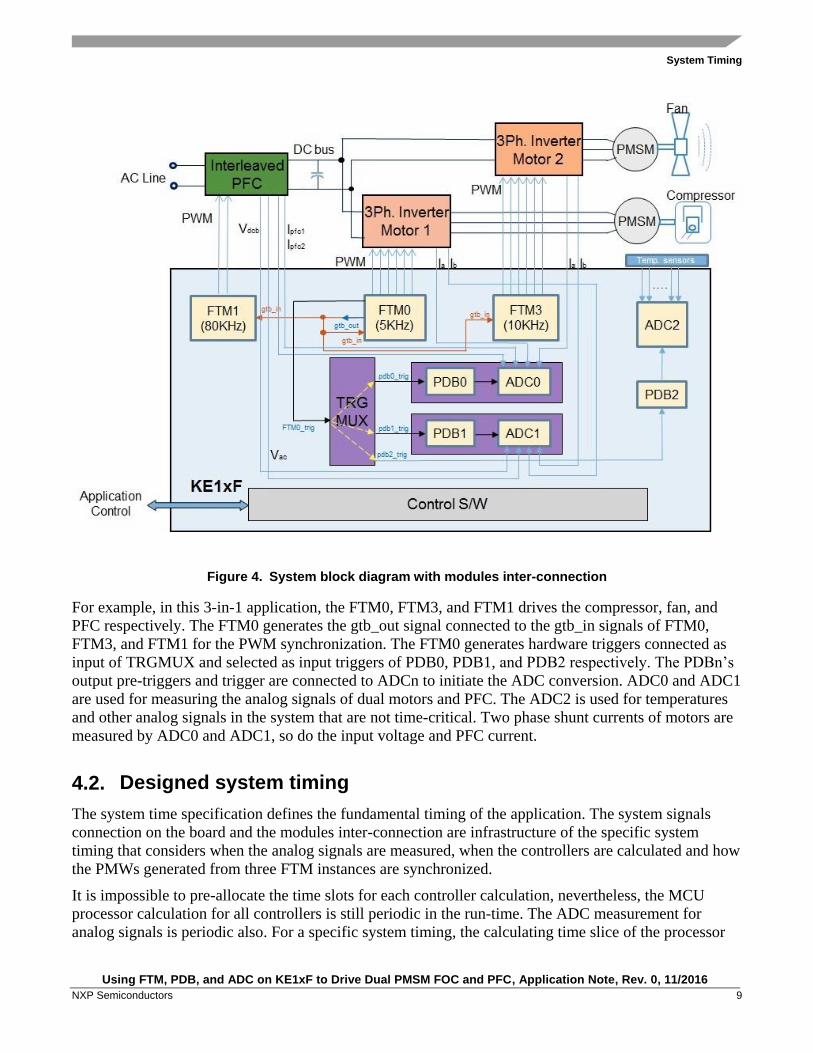
4.1. Peripherals inter-connection
With rich peripherals and their flexible inter-connectivity, it’s easy to implement the complicated timing
to have the KE1xF MCU drive dual sensorless PMSM FOC with PFC. Figure 4 shows the system block
diagram with inter-connection of FTM, PDB, ADC, and TRGMUX for the example application.
System Timing
Using FTM, PDB, and ADC on KE1xF to Drive Dual PMSM FOC and PFC, Application Note, Rev. 0, 11/2016
NXP Semiconductors 9
Figure 4. System block diagram with modules inter-connection
For example, in this 3-in-1 application, the FTM0, FTM3, and FTM1 drives the compressor, fan, and
PFC respectively. The FTM0 generates the gtb_out signal connected to the gtb_in signals of FTM0,
FTM3, and FTM1 for the PWM synchronization. The FTM0 generates hardware triggers connected as
input of TRGMUX and selected as input triggers of PDB0, PDB1, and PDB2 respectively. The PDBn’s
output pre-triggers and trigger are connected to ADCn to initiate the ADC conversion. ADC0 and ADC1
are used for measuring the analog signals of dual motors and PFC. The ADC2 is used for temperatures
and other analog signals in the system that are not time-critical. Two phase shunt currents of motors are
measured by ADC0 and ADC1, so do the input voltage and PFC current.
4.2. Designed system timing
The system time specification defines the fundamental timing of the application. The system signals
connection on the board and the modules inter-connection are infrastructure of the specific system
timing that considers when the analog signals are measured, when the controllers are calculated and how
the PMWs generated from three FTM instances are synchronized.
It is impossible to pre-allocate the time slots for each controller calculation, nevertheless, the MCU
processor calculation for all controllers is still periodic in the run-time. The ADC measurement for
analog signals is periodic also. For a specific system timing, the calculating time slice of the processor

System Timing
Using FTM, PDB, and ADC on KE1xF to Drive Dual PMSM FOC and PFC, Application Note, Rev. 0, 11/2016
10 NXP Semiconductors
calculation period and the measuring time slice of ADC measurement period is defined respectively.
The KE1xF processor running up to 168 MHz is powerful enough to finish all mandatory calculations in
a calculating time slice. The KE1xF 12-bit ADC conversion speed is quick enough to convert all analog
signals during a measuring time slice.
The designed system timing for the example application is shown in Figure 5.
Figure 5. Designed system timing for the example of application
All PWMs for M1, M2, and PFC are center-aligned PWM. The switching frequency of the FTM0 PWM
that drives the M1 (compressor motor) is 5 KHz. The switching frequency of FTM3 PWM for M2 (fan
motor) is 10 kHz. The switching frequency of FTM1 PWMs for PFC is 80 kHz. The ratio of three
witching frequencies is 1:2:8, but the all PWMs do not start from the zero phase at the same time. The
overflow of FTM1 and FTM3 are scheduled elaborately. The FTM1 will start with exactly same phase
as FTM0, and its eight overflow happens exactly in the time of FTM0’s second overflow. The FTM3
first overflow happens exactly in the time when FTM0 counter elapses 12.5 us (1 period of PFC PWM),
that is the second overflow of FTM1 for PFC.
The FTM0 generates two triggers as input of PDB0 and PDB1 through TRGMUX. In the example
application system timing, the initialization trigger, and the external trigger on C7V match are set in
FTM0. Both PDB0 and PDB1 generates eight pre-triggers by eight delay counters to select eight
different ADC configuration registers. The PDB0 output trigger is connected to ADC0 input trigger, and
PDB1 output trigger is connected to ADC1 input trigger. The two connections are configured and work
in parallel and they measure the analog signals simultaneously. All analog signals related to two motors
and PFC are measured by ADC0 and ADC1. To reduce the measure errors caused by PWM switching

System Timing
Using FTM, PDB, and ADC on KE1xF to Drive Dual PMSM FOC and PFC, Application Note, Rev. 0, 11/2016
NXP Semiconductors 11
noise, the ADC measurement points are scheduled close to the as PWM central points as possible. For
PDB2 and ADC2 connection, it is very flexible to configure the delays because all temperature
measurement is slow and not timing-critical. See system signal connection for pin assignment for these
analog signals.
The calculating time slice in the example system timing is 200 us (5 KHz) that is same as PWM period
of compressor motor. The analog measuring time slice is 100 us (10 KHz) that is same as PWM period
of fan motor. Each FTM0 PWM period generates two triggers for PDB to trigger two measuring time
slices. Based on the system time specification, there is one compressor control calculation, two fan
control calculations and four PFC control calculations in one calculating time slice of processor. The
two groups with 16 analog signals are converted in one measuring time slice of ADC.
How to assign the ADC result registers for 16 analog signals is determined by the system timing also. In
this example, the ADCx_R0 (x is 0, 1) are assigned for compressor phase A and phase B current, and
their offsets or values are measured by turns in every other measuring time slice. The ADCx_R1 are for
fan motor two phase current offsets: ADCx_R2 and ADC_R3 are for the interleaved PFC currents and
input voltages; ADCx_R4 are for fan motor two phase currents; ADCx_R5 and ADC_R6 are for the
interleaved PFC currents and input voltages again; the ADCx_R7 is for DC-Bus voltage.
In order to finish all control tasks in one calculating time slice, the specific interrupters are elaborately
scheduled for these calculations respectively. We can use an ISR of ADC conversion complete
interrupts for all calculations, but that’ll increase the interrupt latency. The ADC result register initiating
the conversion complete interrupt requires a check to determine if calculating for the PFC, compressor
or fan control respectively. The good method is to use different hardware interrupt ISRs for different
control objects.
The PFC control calculations will be done in the ISR of the ADC conversion complete interrupt. Only
the interrupts of the 4th and 7th conversion complete in each ADC measuring time slice are enabled. The
fan control calculation is 10 KHz and can be done by PDB0, or PDB1 or PDB3 delay interrupt ISR since
their input trigger are generated with 10 KHz frequency. In this example application, PDB3 delay
interrupt is scheduled with the specific delay value that’s just after the 5th ADC conversion complete in
each ADC measuring time slice, that’s, after the fan motor phase currents are measured.
The compressor control calculation is 5 KHz that is same as the FTM0 PWM switching frequency.
However, the calculation must happen after the compressor motor phase currents are measured. The
time point of the scheduled interrupt must lie in the time after the 1st ADC conversion completes in the
ADC measuring time slice whose trigger is the FTM0 initialization trigger. The 1st ADC conversion
complete in the ADC measuring time slice triggered by the C7V match external trigger is just to
measure the compressor phase current offsets. In the example, the FTM0 channel 6 interrupt will be
enabled and scheduled by setting C6V with specific value to meet the above requirement of timing. The
ISR of FTM0 channel interrupt will calculate the compressor motor control.
The ISRs of interrupts have different priority values by setting 1 for ADC0, 2 for PDB2 and 3 for
FTM0. That means that the PFC calculation has highest priority level, the compressor calculation has
lowest priority level, and the fan calculation has middle priority. As is showed in the Figure 5 also.
4.3. System timing start
How to start the system timing is the key for the system timing working correctly. It includes three
factors:
System Timing
Using FTM, PDB, and ADC on KE1xF to Drive Dual PMSM FOC and PFC, Application Note, Rev. 0, 11/2016
12 NXP Semiconductors
• how to synchronize PWMs
• when to start triggers for ADC
• when to enable the ISRs for calculation
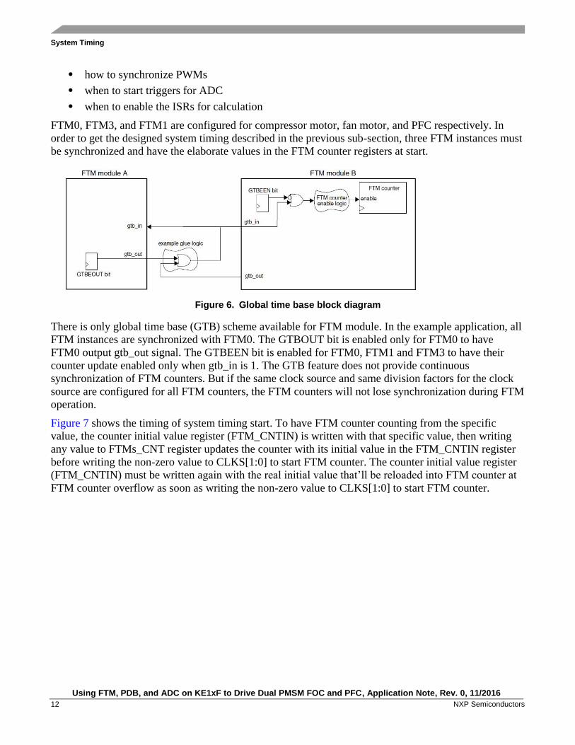
FTM0, FTM3, and FTM1 are configured for compressor motor, fan motor, and PFC respectively. In
order to get the designed system timing described in the previous sub-section, three FTM instances must
be synchronized and have the elaborate values in the FTM counter registers at start.
Figure 6. Global time base block diagram
There is only global time base (GTB) scheme available for FTM module. In the example application, all
FTM instances are synchronized with FTM0. The GTBOUT bit is enabled only for FTM0 to have
FTM0 output gtb_out signal. The GTBEEN bit is enabled for FTM0, FTM1 and FTM3 to have their
counter update enabled only when gtb_in is 1. The GTB feature does not provide continuous
synchronization of FTM counters. But if the same clock source and same division factors for the clock
source are configured for all FTM counters, the FTM counters will not lose synchronization during FTM
operation.
Figure 7 shows the timing of system timing start. To have FTM counter counting from the specific
value, the counter initial value register (FTM_CNTIN) is written with that specific value, then writing
any value to FTMs_CNT register updates the counter with its initial value in the FTM_CNTIN register
before writing the non-zero value to CLKS[1:0] to start FTM counter. The counter initial value register
(FTM_CNTIN) must be written again with the real initial value that’ll be reloaded into FTM counter at
FTM counter overflow as soon as writing the non-zero value to CLKS[1:0] to start FTM counter.

Modules Configuration
Using FTM, PDB, and ADC on KE1xF to Drive Dual PMSM FOC and PFC, Application Note, Rev. 0, 11/2016
NXP Semiconductors 13
Figure 7. System timing start method
Both, the FTM0 initialization trigger and the external trigger on C7V match are disabled in the
initialization routine. All interrupts are disabled also except for the FTM0 channel 6 matching interrupt.
After starting the system timing by setting the FTM0 CLKS[1:0] != 0:0, the PWMs are enabled but their
output are disabled, so do FTM triggers and interrupts. In the C6V matching ISR, the triggers and
interrupts are enabled. The triggers will be generated for ADC conversions from the second ADC
measuring time slice. In Figure 7, it shows that the first 100us period after enabling the FTM0 is for
system start processing. The effective system timing does work after 100 us.
5. Modules Configuration
5.1. PWM configuration for M1
There are some macros are defined for the FTM0 configuration. The clock configuration of the example
application is set as High Speed RUN mode. The system clock is 168 MHz is routed as peripheral
interface clock for FTM module by PCC module. At last it is selected as FTM input clock by setting
CLKS[1:0] = 01 and PS[2:0] = 0; The PWM modulo to generate 5 KHz PWM is derived from the
168-MHz FTM input clock. So the modulo is 168 MHz / 5 kHz = 33600 ticks. The deadtime inserted is
about 16*20/168 MHz ≈2 us. The turn-on time and turn-off time are determined by the IPM component
mounted on the board that can be measured offline.
Modules Configuration
Using FTM, PDB, and ADC on KE1xF to Drive Dual PMSM FOC and PFC, Application Note, Rev. 0, 11/2016
14 NXP Semiconductors
/* Constant definition for 5KHz Motor 1 */
#define M1_MODULO_HALF 16800
#define M1_DEADTIME_VAL 20
#define M1_FTM_CNT_START (-M1_MODULO_HALF)
#define M1_DEADTIME_PS 3
#define M1_DEADTIME (16*20)
#define M1_IMP_UP 189
#define M1_IMP_DOWN 445
#define M1_ADC_DELAY ((M1_IMP_DOWN+M1_IMP_UP+M1_DEADTIME)/2)
#define M1_DISABLE_PWM_OUTPUT() FTM0->SC &= ~(FTM_SC_PWMEN0_MASK | FTM_SC_PWMEN1_MASK |
FTM_SC_PWMEN2_MASK\
| FTM_SC_PWMEN3_MASK | FTM_SC_PWMEN4_MASK |
FTM_SC_PWMEN5_MASK)
#define M1_ENABLE_PWM_OUTPUT() FTM0->SC |= (FTM_SC_PWMEN0_MASK | FTM_SC_PWMEN1_MASK |
FTM_SC_PWMEN2_MASK\ | FTM_SC_PWMEN3_MASK |
FTM_SC_PWMEN4_MASK | FTM_SC_PWMEN5_MASK)
The FTM0 instance is configured to drive compressor motor. It is necessary to enable FTM0 clock by
configuring the PCC FLEXTMR0 register (PCC_FLEXTMR0) from the Peripheral Clock Controller
module (PCC).
The following syntax is used to enable the clock for FTM0:
BITBAND_ACCESS32(&PCC_FLEXTMR0, PCC_CLKCFG_CGC_SHIFT) = 1;
Disable the write-protection and enable the FTM that’s different from compatible TPM behavior.
/* Disable the write-protection */
BITBAND_ACCESS32(&FTM0->MODE, FTM_MODE_WPDIS_SHIFT) = 1;
/* Enable FTM */
BITBAND_ACCESS32(&FTM0->MODE, FTM_MODE_FTMEN_SHIFT) = 1;
The counter runs in the functional mode; the initialization trigger is generated on the counter wrap event.
The PWM reload frequency is set every reload opportunity.
/* Counter running in the functional mode, ITRIGR=0; LDFQ=0 */
FTM0->CONF = FTM_CONF_BDMMODE(3);
The over-current signal is connected to the FTM0 fault signal with active low polarity according to the
hardware. It’s necessary to enable the fault control and set automatic fault clearing. The fault interrupt is
disabled. The following code configures the fault:
/* Enable fault control and automatic fault clearing */
FTM0->MODE |= FTM_MODE_FAULTM_MASK;
/* Disable fault interrupt */
BITBAND_ACCESS32(&FTM0->MODE, FTM_MODE_FAULTIE_SHIFT) = 0;
/* Active low polarity for fault 3 */
FTM0->FLTPOL = FTM_FLTPOL_FLT3POL_MASK;
/* Enable fault3, fault filter 5 system clocks, output safe state for fault */
FTM0->FLTCTRL = FTM_FLTCTRL_FFVAL(5) | FTM_FLTCTRL_FFLTR3EN_MASK | FTM_FLTCTRL_FAULT3EN_MASK;
The each pair of channels are configured as symmetrical PWM in the combine mode and
complementary mode. The PWM update synchronization, fault control and deadtime insertion in the
pair of channels are enabled. The channel (6) and channel (7) are configured as the combine mode even

Modules Configuration
Using FTM, PDB, and ADC on KE1xF to Drive Dual PMSM FOC and PFC, Application Note, Rev. 0, 11/2016
NXP Semiconductors 15
without PWM output to avoid input capture mode. Each pair of channels in the FTM0 are configured
using the following syntax:
FTM0->COMBINE = FTM_COMBINE_FAULTEN0_MASK | FTM_COMBINE_SYNCEN0_MASK | FTM_COMBINE_DTEN0_MASK
| FTM_COMBINE_COMP0_MASK | FTM_COMBINE_COMBINE0_MASK
| FTM_COMBINE_FAULTEN1_MASK | FTM_COMBINE_SYNCEN1_MASK | FTM_COMBINE_DTEN1_MASK
| FTM_COMBINE_COMP1_MASK | FTM_COMBINE_COMBINE1_MASK
| FTM_COMBINE_FAULTEN2_MASK | FTM_COMBINE_SYNCEN2_MASK | FTM_COMBINE_DTEN2_MASK
| FTM_COMBINE_COMP2_MASK | FTM_COMBINE_COMBINE2_MASK |
FTM_COMBINE_COMBINE3_MASK;
The FTM counter initial value register CNTIN will be set up to the negative value of the half modulo.
The FTM modulo register MOD is set as the positive value of the half modulo -1.
/* Set PWM frequency */
FTM0->MOD = M1_MODULO_HALF-1;
FTM0->CNTIN = M1_FTM_CNT_START;
The deadtime insertion is set. The channel (n) outputs is forced low at the beginning of the period and on
the channel (n+1) match (CNT = C(n+1)V), and forced high on the channel (n) match (CNT = C(n)V).
The PWM duty is initialized as center-aligned with 50 % duty.
/* Deadtime = PS*VAL*/
FTM0->DEADTIME = FTM_DEADTIME_DTPS(M1_DEADTIME_PS) |FTM_DEADTIME_DTVAL(M1_DEADTIME_VAL);
/* ELSnB:ELSnA = 1:0, the channle(n) ouput is forced low at the beginning of
* the period and on the channle(n+1) match (CNT = C(n+1)V). It's forced high
* on the channel(n) match (CNT = C(n)V).
*/
BITBAND_ACCESS32(&FTM0->CONTROLS[0].CnSC, FTM_CnSC_ELSB_SHIFT) = 1;
BITBAND_ACCESS32(&FTM0->CONTROLS[1].CnSC, FTM_CnSC_ELSB_SHIFT) = 1;
BITBAND_ACCESS32(&FTM0->CONTROLS[2].CnSC, FTM_CnSC_ELSB_SHIFT) = 1;
BITBAND_ACCESS32(&FTM0->CONTROLS[3].CnSC, FTM_CnSC_ELSB_SHIFT) = 1;
BITBAND_ACCESS32(&FTM0->CONTROLS[4].CnSC, FTM_CnSC_ELSB_SHIFT) = 1;
BITBAND_ACCESS32(&FTM0->CONTROLS[5].CnSC, FTM_CnSC_ELSB_SHIFT) = 1;
/* Initialize PWM with centeral aligned, 50% duty */
FTM0->CONTROLS[0].CnV = -M1_MODULO_HALF/2;
FTM0->CONTROLS[1].CnV = M1_MODULO_HALF/2 - 1;
FTM0->CONTROLS[2].CnV = -M1_MODULO_HALF/2;
FTM0->CONTROLS[3].CnV = M1_MODULO_HALF/2 - 1;
FTM0->CONTROLS[4].CnV = -M1_MODULO_HALF/2;
FTM0->CONTROLS[5].CnV = M1_MODULO_HALF/2 - 1;
The channel 7 match is enabled to trigger the PDB, is set up to 0 to generate a trigger in
the middle of PWM period. This trigger is ORed together with initialization trigger as input
trigger of the PDB through TRGMUX module. The channel 6 register is set up to the value of
Modules Configuration
Using FTM, PDB, and ADC on KE1xF to Drive Dual PMSM FOC and PFC, Application Note, Rev. 0, 11/2016
16 NXP Semiconductors
time after the compressor phase current measurement is done as well as the compressor control
is calculated as early as possible./* Set Channel 7 to tigger the PDB0 and PDB1 */
FTM0->CONTROLS[7].CnV = 0; // Middle of PWM peroid
/* Set Channel 6 to schedule an interrupt to start triggers or motor 1 calculation */
FTM0->CONTROLS[6].CnV = -M1_MODULO_HALF + M1_CALCULATE_INT_DELAY;
The channel 6 interrupt is enabled whose ISR is installed to enable triggers and interrupt to start the
system timing. Below is the way how to configure C6V interrupt and set LDOK bit before running
PWM.
/* Disable PWM channel output ports */
M1_DISABLE_PWM_OUTPUT();
/* Clear CH6 interrupt flag */
FTM0->CONTROLS[6].CnSC &= ~FTM_CnSC_CHF_MASK;
/* Enable CH6 interrupt to start input triggers of PDB */
BITBAND_ACCESS32(&FTM0->CONTROLS[6].CnSC, FTM_CnSC_CHIE_SHIFT) = 1;
/* Configure NVIC for FTM0 interrupt */
NVIC_EnableIRQ(FTM0_IRQn);
NVIC_SetPriority(FTM0_IRQn, ISR_PRIORITY_FTM0);
/* Set LDOK bit */
BITBAND_ACCESS32(&FTM0->PWMLOAD, FTM_PWMLOAD_LDOK_SHIFT) = 1;
The PWM output is disabled during the initialization. The PWM isn’t generated now because the input
clock of FTM is still disabled now.
5.2. PWM configuration for M2
The FTM3 instance is configured for fan compressor whose configurations are almost same as that for
FTM0 instance for compressor. The switching frequency of PWM for fan motor is 10 kHz. So the
modulo is 168 MHz / 10 kHz = 16800 ticks. As a result, the counter initial register CNTIN is -8400 and
MOD register is 8400-1. The second difference is the channel 6 and channel 7 value registers aren’t used
and there’s no interrupt enabled for FTM3. The last difference is the fault input number.
The macros related to FTM3 generating PWM for fan motor are listed as below:
Modules Configuration
Using FTM, PDB, and ADC on KE1xF to Drive Dual PMSM FOC and PFC, Application Note, Rev. 0, 11/2016
NXP Semiconductors 17
/* Constant definition for 10KHz Motor 2 */
#define M2_MODULO_HALF 8400
#define M2_DEADTIME_VAL 16
#define M2_FTM_CNT_START (-M2_MODULO_HALF/4)
#define M2_DEADTIME_PS 3
#define M2_DEADTIME (16*16)
#define M2_IMP_UP 168
#define M2_IMP_DOWN 448
#define M2_ADC_DELAY ((M2_IMP_DOWN+M2_IMP_UP+M2_DEADTIME)/2) // H/w propagation delay
#define M2_DISABLE_PWM_OUTPUT() FTM3->SC &= ~(FTM_SC_PWMEN0_MASK | FTM_SC_PWMEN1_MASK |
FTM_SC_PWMEN2_MASK\
| FTM_SC_PWMEN3_MASK | FTM_SC_PWMEN4_MASK | FTM_SC_PWMEN5_MASK)
#define M2_ENABLE_PWM_OUTPUT() FTM3->SC |= (FTM_SC_PWMEN0_MASK | FTM_SC_PWMEN1_MASK |
FTM_SC_PWMEN2_MASK\
| FTM_SC_PWMEN3_MASK | FTM_SC_PWMEN4_MASK | FTM_SC_PWMEN5_MASK)
5.3. PWM configuration for interleaved PFC
There are two MOSFETs used to drive the interleaved PFC in the application. The PWM signals for two
MOSFETs will be center-aligned and shifted 180 degree to each other. A pair of channels cannot output
two PWMs with 180 degree shift to each other. Two pairs of channels are used to generate two center-
aligned PWMs with 180 degree shift to each other in the application.
The frequency of the PWM of PFC will be 80 KHz. In order to generate 80 KHz, the PWM modulo will
be 168 MHz / 80 KHz = 2100 ticks. The following macros are defined for FTM1 counter initial value
register and mode value register:
#define PFC_MODULO_HALF 1050 // 80KHz
#define PFC_FTM_CNT_START (-PFC_MODULO_HALF)
#define PFC_DISABLE_PWM_OUTPUT() FTM1->SC &= ~(FTM_SC_PWMEN0_MASK | FTM_SC_PWMEN4_MASK)
#define PFC_ENABLE_PWM_OUTPUT() FTM1->SC |= (FTM_SC_PWMEN0_MASK | FTM_SC_PWMEN4_MASK)
The first step is enable FTM1 clock by configuring the PCC FLEXTMR1 register (PCC_FLEXTMR1)
from the Peripheral Clock Controller module (PCC). The following syntax is used to enable the clock
for FTM1:
/* Enable the FTM1 clock */
BITBAND_ACCESS32(&PCC_FLEXTMR1, PCC_CLKCFG_CGC_SHIFT) = 1;
The FTM function is enabled and write-projection mode is disabled. The counter runs in the functional
mode; The PWM reload frequency is set every reload opportunity. There’re 3 fault inputs for the FTM1
modules that are DC-Bus over-voltage fault and two over-current faults. They all are active low polarity
faults and are connected to the input fault 0, fault 2 and fault3.
Below is the code how to configure these features:
Modules Configuration
Using FTM, PDB, and ADC on KE1xF to Drive Dual PMSM FOC and PFC, Application Note, Rev. 0, 11/2016
18 NXP Semiconductors
/* Disable the write-protection */
BITBAND_ACCESS32(&FTM1->MODE, FTM_MODE_WPDIS_SHIFT) = 1;
/* Enable FTM */
BITBAND_ACCESS32(&FTM1->MODE, FTM_MODE_FTMEN_SHIFT) = 1;
/* Counter running in the debug mode */
FTM1->CONF |= FTM_CONF_BDMMODE(3);
/* Enable fault control and automatic fault clearing */
FTM1->MODE |= FTM_MODE_FAULTM_MASK;
/* Disable fault interrupt */
BITBAND_ACCESS32(&FTM1->MODE, FTM_MODE_FAULTIE_SHIFT) = 0;
/* Active high polarity for fault 0, 2, 3 */
FTM1->FLTPOL = 0;
/* Enable fault0, 2, 3, fault fliter 5 system clocks, output safe state for fault */
FTM1->FLTCTRL = FTM_FLTCTRL_FFVAL(5) | FTM_FLTCTRL_FFLTR0EN_MASK | FTM_FLTCTRL_FAULT0EN_MASK
| FTM_FLTCTRL_FFLTR2EN_MASK | FTM_FLTCTRL_FAULT2EN_MASK
| FTM_FLTCTRL_FFLTR3EN_MASK | FTM_FLTCTRL_FAULT3EN_MASK;
The pair of channel 0 and channel 1 is configured as combine and complementary mode. PWM update
synchronization and fault control are enabled also. No deadtime is inserted in the PWM for PFC. Same
configuration is for the pair of channel 4 and channel 5. Despite two pairs of channels are configure,
only the outputs of channel 0 and channel 4 are used as two PWM to drive PFC. In order to implement
two PWMs with180 degree ship to each other, the channel 0 output is forced low at the beginning of the
PWM period and on the event that the FTM1 counter value matches channel 1 value register
(CNT=C1V). The output is set high on the event that the FTM1 counter value matches the channel 0
value register (CNT=C0V). It’s done by setting ELSB:ELSA = 1:0. On the other hand, the channel 4
output is forced high at the beginning of the period and on the event that the FTM1 counter value
matches channel 5 value register (CNT=C5V). The output is cleared low on the event that the FTM1
counter value matches the channel 4 value register (CNT=C4V). It’s done by setting ELSB:ELSA = x:1.
The following syntax is used to configure the PWM edge or level features:
Modules Configuration
Using FTM, PDB, and ADC on KE1xF to Drive Dual PMSM FOC and PFC, Application Note, Rev. 0, 11/2016
NXP Semiconductors 19
/* Center aligned PWM is used in combine mode
* COMBINE = 1 - combine mode set
* COMP = 1 - complementary PWM set
* SYNCEN = 1 - PWM update synchronization enabled
* FAULTEN = 1 - fault control enabled
*/
FTM1->COMBINE = FTM_COMBINE_FAULTEN0_MASK | FTM_COMBINE_SYNCEN0_MASK
| FTM_COMBINE_COMP0_MASK | FTM_COMBINE_COMBINE0_MASK
| FTM_COMBINE_FAULTEN2_MASK | FTM_COMBINE_SYNCEN2_MASK
| FTM_COMBINE_COMP2_MASK | FTM_COMBINE_COMBINE2_MASK;
/* Set PWM frequency */
FTM1->MOD = PFC_MODULO_HALF-1;
FTM1->CNTIN = PFC_FTM_CNT_START;
/* ELSnB:ELSnA = 1:0, the channle(n) ouput is forced low at the beginning of
* the period and on the channle(n+1) match (CNT = C(n+1)V). It's forced high
* on the channel(n) match (CNT = C(n)V).
* ELSnB:ELSnA = x:1, the channle(n) ouput is forced high at the beginning of
* the period and on the channle(n+1) match (CNT = C(n+1)V). It's forced low
* on the channel(n) match (CNT = C(n)V).
* Set ELSnB:ELSnA = 1:0 for one PWM and ELSnB:ELSnA = x:1 for another PWM to
* to implement 180 degree phase shift between two PWMs for interleave PFC
*/
BITBAND_ACCESS32(&FTM1->CONTROLS[0].CnSC, FTM_CnSC_ELSB_SHIFT) = 1;
BITBAND_ACCESS32(&FTM1->CONTROLS[1].CnSC, FTM_CnSC_ELSB_SHIFT) = 1;
BITBAND_ACCESS32(&FTM1->CONTROLS[4].CnSC, FTM_CnSC_ELSA_SHIFT) = 1;
BITBAND_ACCESS32(&FTM1->CONTROLS[5].CnSC, FTM_CnSC_ELSA_SHIFT) = 1;
The PWMs are initialized with 0% duty. Below is the way how to set 0% duty for two PWM with 180
degree shift to each other:
/* Initialize PWM with centeral aligned, 0% duty */
FTM1->CONTROLS[0].CnV = -PFC_MODULO_HALF/2;
FTM1->CONTROLS[1].CnV = -PFC_MODULO_HALF/2;
FTM1->CONTROLS[4].CnV = -PFC_MODULO_HALF;
FTM1->CONTROLS[5].CnV = PFC_MODULO_HALF;
/* Initialize the channel output */
BITBAND_ACCESS32(&FTM1->MODE, FTM_MODE_INIT_SHIFT) = 1;
The output is disabled after initialization and last step is to set LDOK bit before running FTM1.
/* Disable PWM channel output ports */
PFC_DISABLE_PWM_OUTPUT();
/* Set LDOK bit */
BITBAND_ACCESS32(&FTM1->PWMLOAD, FTM_PWMLOAD_LDOK_SHIFT) = 1;
In order to generate two PWMs with 180 degree shift to each other, the special method is required to
calculate the channel values for a given duty percent value derived from the control calculation. The
calculated values are written to the FTM1 channel value registers before next reload point. The inline
function is given below that’s responsible for channel value calculation and PWM update before next
reload happens.

Modules Configuration
Using FTM, PDB, and ADC on KE1xF to Drive Dual PMSM FOC and PFC, Application Note, Rev. 0, 11/2016
20 NXP Semiconductors
inline void PFC_PWM_UPDATE(GMCLIB_2COOR_T_F16 *psDuty)
{
int16_t w16ModuloHalf = PFC_MODULO_HALF;
int16_t w16Result;
/* Duty cycle limit [0 to 0.9] */
if (!psDuty->f16A) /* 0% duty cycle */
{
FTM1->CONTROLS[0].CnV = -PFC_MODULO_HALF/2;
FTM1->CONTROLS[1].CnV = -PFC_MODULO_HALF/2;
FTM1->CONTROLS[4].CnV = -PFC_MODULO_HALF;
FTM1->CONTROLS[5].CnV = PFC_MODULO_HALF;
}
else
{
/* PWM channel 0 */
w16Result = MLIB_Mul_F16(psDuty->f16A, w16ModuloHalf);
FTM1->CONTROLS[0].CnV = -w16Result;
FTM1->CONTROLS[1].CnV = w16Result;
/* PWM channel 4 */
w16Result = MLIB_Mul_F16(32767 - psDuty->f16B, w16ModuloHalf);
FTM1->CONTROLS[4].CnV = -w16Result;
FTM1->CONTROLS[5].CnV = w16Result;
}
/* Set LDOK bit */
BITBAND_ACCESS32(&FTM1->PWMLOAD, FTM_PWMLOAD_LDOK_SHIFT) = 1;
}
5.4. PWM synchronization
The FTM GTB scheme is used to synchronize the PWMs at the system start. The first step is to set
GTBEEN bit for FTM0, FTM1 and FTM3 to have FTM counter updated only when its gtb_in signal is
1.
The following syntax is to set it for them:
/* Enable GTBEEN for FTM0, FTM1 and FTM3 */
FTM0->CONF |= FTM_CONF_GTBEEN_MASK;
FTM1->CONF |= FTM_CONF_GTBEEN_MASK;
FTM3->CONF |= FTM_CONF_GTBEEN_MASK;
The FTM0, FTM1 and FTM3 counter initial values are written to their initial value registers during
configuration. Now writing any value to the counter register updates the counter value with the value in
its initial value register, CNTIN.
The configuration looks like:
Modules Configuration
Using FTM, PDB, and ADC on KE1xF to Drive Dual PMSM FOC and PFC, Application Note, Rev. 0, 11/2016
NXP Semiconductors 21
FTM0->CNT = M1_MODULO_HALF;
FTM1->CNT = PFC_MODULO_HALF;
FTM3->CNT = M2_MODULO_HALF;
Now selecting the FTM input clock as FTM counter clock source with 1 divider for all FTMs. It can be
done by the way shown below:
/* Select the system clock with 1 divider for all FTMs */
FTM0->SC |= FTM_SC_CLKS(1);
FTM1->SC |= FTM_SC_CLKS(1);
FTM3->SC |= FTM_SC_CLKS(1);
The FTM clock is enabled, but the counter is still disabled due to the enabled GTBEEN bit. Now all
FTM instances with configured features are ready for starting. Setting the FTM0 GTBEOUT to 1
generates the global time base signal and enables the FTM0, FTM1 and FTM3 counters count from their
initial value synchronically. Below shows the code of setting:
/* Set FTM0 GTBEOUT to generate the global time base signal */
FTM0->CONF |= FTM_CONF_GTBEOUT_MASK;
The PWM period is determined by the value written in the CNTIN register and MOD register. The three
initial value register must be updated with the negative value of half modulo as soon as the three FTM
counters are enabled by setting FTM0 GTBEOUT bit. The initial value written in the initialization
function is just to update the counter value with specific value at the start. At the last step, the negative
value of half modulo must be written to the CNTIN register to determine the PWM period. Below is the
way how to write three FTM CNTIN registers:
/* Set the FTM1 and FTM3 Counter initial value */
FTM1->CNTIN = - PFC_MODULO_HALF;
FTM3->CNTIN = - M2_MODULO_HALF;
FTM0->CNTIN = - M1_MODULO_HALF;
5.5. TRGMUX configuration
KE1xF has a TRGMUX that provides a module interconnectivity scheme. Only FTM0 is set up to
generate the initialization trigger and the external trigger on the channel (7) match. The two FTM
triggers are ORed into one input trigger of TRGMUX in the chip design. This input trigger is selected as
PDB input trigger by configuring the TRGMUX. The PDB input trigger will generate 8 pre-triggers and
triggers. The eight pre-trigger signals are connected to the ADC module to select the corresponding
ADC configuration registers and result registers. Eight trigger signals are ORed into one trigger in the
PDB that’s connected to ADC input trigger to trigger the ADC conversion. Only selecting the input
trigger for PDB needs configuration by software. Other connections are done by hardware design in the
chip. The following code show how to select the input trigger for PDB0, PDB1 and PBD2 respectively
in the application:

Modules Configuration
Using FTM, PDB, and ADC on KE1xF to Drive Dual PMSM FOC and PFC, Application Note, Rev. 0, 11/2016
22 NXP Semiconductors
/* Enable the TRGMUX clock */
BITBAND_ACCESS32(&PCC_TRGMUX, PCC_CLKCFG_CGC_SHIFT) = 1;
/* Mux ACMP0_OUT (TRGMUX_IN17) to TRGMUX_EXTOUT7(TRGMUX_OUT11) */
TRGMUX0->TRGCFG[TRGMUX_EXTOUT1_INDEX] |= TRGMUX_TRGCFG_SEL3(17);
/* Mux FTM0_TRIG(TRGMUX0_IN11) to PDB0_TRG_IN (TRGMUX_OUT56) */
TRGMUX0->TRGCFG[TRGMUX_PDB0_INDEX] |= TRGMUX_TRGCFG_SEL0(11);
/* Mux FTM0_TRIG(TRGMUX0_IN11) to PDB1_TRG_IN (TRGMUX_OUT60) */
TRGMUX0->TRGCFG[TRGMUX_PDB1_INDEX] |= TRGMUX_TRGCFG_SEL0(11);
/* Mux FTM0_TRIG(TRGMUX0_IN11) to PDB2_TRG_IN (TRGMUX_OUT60) */
TRGMUX0->TRGCFG[TRGMUX_PDB2_INDEX] |= TRGMUX_TRGCFG_SEL0(11);
5.6. PDB configuration
The PDB0 and PDB1 are configured to generate the pre-triggers and trigger to trigger the ADC0 and
ADC1 conversion respectively. They work in parallel. So the configuration of them are same except the
PDB0 error interrupt is enabled but PDB1 has no interrupt enabled. The PDB2 is configured similar to
the PDB0 but only to generate an interrupt with predefined delay from the input triggers. The
configuration for details will be given in the following content.
The first step is to enable the PDB module clock by configure the PCC_PDB0 register from the
Peripheral Clock Controller module (PCC). Below is the way how to enable PDB0 clock:
/* Enable the PDB0 clock */
BITBAND_ACCESS32(&PCC_PDB0, PCC_CLKCFG_CGC_SHIFT) = 1;
The input of PDB is sourced from FTM0, and all delays for pre-trigger, trigger and delay interrupt are
based on the input trigger. The mod of PDB isn’t used and is set up to maximal value, that’s 0xFFFF.
/* Set the modulus register with max value */
PDB0->MOD = 0xFFFF;
The PDB internal registers are loaded with the values from their buffers when the trigger input event is
detected after 1 is written to LDOK bit. The input clock is set exactly same as system clock, that’s 168
MHz. The trigger input source 0 is selected since hardware design has only one trigger input from
TRGMUX. Below is the way to configure the PDB features.
For PDB0, the error interrupt is enabled.
/* LDMOD=b10, PDBEIE=1, TRGSEL=0(TRGMUX_PDB_TRIG), PRESCALER=0, MULT=0, CONT=0, PDBEN=1*/
PDB0->SC = PDB_SC_LDMOD(2) | PDB_SC_PDBEIE(1) | PDB_SC_TRGSEL(0) | PDB_SC_PDBEN_MASK;
For PDB1:
/* LDMOD=b10, TRGSEL=0, PRESCALER=0, MULT=0, CONT=0, PDBEN=1*/
PDB1->SC = PDB_SC_LDMOD(2) | PDB_SC_TRGSEL(0) | PDB_SC_PDBEN_MASK;
For DPB2:

Modules Configuration
Using FTM, PDB, and ADC on KE1xF to Drive Dual PMSM FOC and PFC, Application Note, Rev. 0, 11/2016
NXP Semiconductors 23
/* LDMOD=b10, TRGSEL=0, PRESCALER=0, MULT=0, CONT=0, PDBEN=1*/
PDB2->SC = PDB_SC_LDMOD(2) | PDB_SC_TRGSEL(0) | PDB_SC_PDBEN_MASK;
The pre-trigger bypass mode is disabled since all 8 delay registers are used to generate eight pre-
triggers. The delayed values are predefined based on the system timing design how to arrange the analog
signal measurement done. See the system timing figure above for details.
The following is the macros used in the PDB configurations.
/* Constant for PDB settings */
#define PDB01_CH0_DELAY_USED 0xFF // Total 8 channels are used
#define M2_CALCULATE_INT_DELAY (PDB01_CH0DLY4_VALUE+315)
#define M1_CALCULATE_INT_DELAY (M1_ADC_DELAY+315)
#define PDB01_CH0DLY0_VALUE M1_ADC_DELAY
#define PDB01_CH0DLY1_VALUE (PFC_MODULO_HALF/2*4+M2_ADC_DELAY)
#define PDB01_CH0DLY2_VALUE (PFC_MODULO_HALF/2*8)
#define PDB01_CH0DLY3_VALUE (PFC_MODULO_HALF/2*10)
#define PDB01_CH0DLY4_VALUE (PFC_MODULO_HALF/2*20+M2_ADC_DELAY)
#define PDB01_CH0DLY5_VALUE (PFC_MODULO_HALF/2*24)
#define PDB01_CH0DLY6_VALUE (PFC_MODULO_HALF/2*26)
#define PDB01_CH0DLY7_VALUE (PFC_MODULO_HALF/2*26+480)
The syntax to configure the PDB delays for DPB0 and PDB1 is given below.
For PDB0:
/* Set the pre-trigger delay register effective (DLY0~DLY7)*/
PDB0->CH[0].C1 = PDB_C1_TOS(PDB01_CH0_DELAY_USED) | PDB_C1_EN(PDB01_CH0_DELAY_USED);
/* Set channel delay for the pre-trigger */
PDB0->CH[0].DLY[0] = PDB01_CH0DLY0_VALUE;
PDB0->CH[0].DLY[1] = PDB01_CH0DLY1_VALUE;
PDB0->CH[0].DLY[2] = PDB01_CH0DLY2_VALUE;
PDB0->CH[0].DLY[3] = PDB01_CH0DLY3_VALUE;
PDB0->CH[0].DLY[4] = PDB01_CH0DLY4_VALUE;
PDB0->CH[0].DLY[5] = PDB01_CH0DLY5_VALUE;
PDB0->CH[0].DLY[6] = PDB01_CH0DLY6_VALUE;
PDB0->CH[0].DLY[7] = PDB01_CH0DLY7_VALUE;
For PDB1:

Modules Configuration
Using FTM, PDB, and ADC on KE1xF to Drive Dual PMSM FOC and PFC, Application Note, Rev. 0, 11/2016
24 NXP Semiconductors
/* Set the pre-trigger delay register effective (DLY0~DLY7)*/
PDB1->CH[0].C1 = PDB_C1_TOS(PDB01_CH0_DELAY_USED) | PDB_C1_EN(PDB01_CH0_DELAY_USED);
/* LDMOD=b10, TRGSEL=0, PRESCALER=0, MULT=0, CONT=0, PDBEN=1*/
PDB1->SC = PDB_SC_LDMOD(2) | PDB_SC_TRGSEL(0) | PDB_SC_PDBEN_MASK;
/* Set channel delay for the pre-trigger */
PDB1->CH[0].DLY[0] = PDB01_CH0DLY0_VALUE;
PDB1->CH[0].DLY[1] = PDB01_CH0DLY1_VALUE;
PDB1->CH[0].DLY[2] = PDB01_CH0DLY2_VALUE;
PDB1->CH[0].DLY[3] = PDB01_CH0DLY3_VALUE;
PDB1->CH[0].DLY[4] = PDB01_CH0DLY4_VALUE;
PDB1->CH[0].DLY[5] = PDB01_CH0DLY5_VALUE;
PDB1->CH[0].DLY[6] = PDB01_CH0DLY6_VALUE;
PDB1->CH[0].DLY[7] = PDB01_CH0DLY7_VALUE;
PDB0 enables the error interrupt to process the case of PDB sequence error. The ADC coco signal is
sent to PDB and the PDB lock state is deactivated after the conversion is done by reading the converted
value in the result register. If another per-trigger signal is detected while the PDB is not deactivated,
thePDB sequence error interrupt is generated. It is important to process such error interrupt. Because the
PFC control calculation is done in the ADC conversion interrupt that’s triggered by PDB. If error
happens, PDB-ADC trigger scheme stops and there is no ADC interrupt any more. As a result, the PWM
to drive PFC MOSFET will stop to update and MOSFETs are damaged.
The following code is to configure the interrupt for PDB0.
/* Clear PDB0 interrupt flag */
BITBAND_ACCESS32(&PDB0->SC, PDB_SC_PDBIF_SHIFT) = 0;
/* Configure NVIC for PDB0 interrupt */
NVIC_EnableIRQ(PDB0_IRQn);
NVIC_SetPriority(PDB0_IRQn, ISR_PRIORITY_PDB0);
PDB2 enables the delay interrupt to calculate the fan motor control calculation. The delayed value is
predefined based on the motor phase current measurement time point. The interrupt is enabled in the
FTM0 C6V matching ISR at the system timing start stage. Below is the code of configure it:
/* Schedule the PDB interrupt delay to calculate M2 controllers */
PDB2->IDLY = M2_CALCULATE_INT_DELAY;
/* Clear PDB2 interrupt flag */
BITBAND_ACCESS32(&PDB2->SC, PDB_SC_PDBIF_SHIFT) = 0;
/* Configure NVIC for PDB2 interrupt */
NVIC_EnableIRQ(PDB2_IRQn);
NVIC_SetPriority(PDB2_IRQn, ISR_PRIORITY_PDB2);
The last step is to set LDOK bit to update the PDB registers from their internal buffers written
previously.
The following is the code to set LDOK bit for PDB0
Modules Configuration
Using FTM, PDB, and ADC on KE1xF to Drive Dual PMSM FOC and PFC, Application Note, Rev. 0, 11/2016
NXP Semiconductors 25
/* Set LDOK for PDB0 */
BITBAND_ACCESS32(&PDB0->SC, PDB_SC_LDOK_SHIFT) = 1;
5.7. ADC configuration
ADC0 and ADC1 are used to convert all timing-critical analog signals. Two ADC instances have almost
same configurations since they always work in parallel with same ways. But the ADC0 enables the
conversion complete interrupt on some results but no interrupt enabled for ADC1. Another difference is
input channel selection. The ADC clock configuration, sample time and voltage reference select, self-
calibration, etc configured for ADC0 here work for ADC1 also. Only the difference part for ADC1 will
be given here.
The ADC first four pre-triggers and trigger can be configured different trigger sources. It’s from PDB by
default.
It is configured explicitly here as in the following code snippet.
/* The first 4 pre-triggers and triggers are all from PDB (default) */
SIM->ADCOPT = SIM_ADCOPT_ADC0TRGSEL(0) | SIM_ADCOPT_ADC0PRETRGSEL(0)
| SIM_ADCOPT_ADC1TRGSEL(0) | SIM_ADCOPT_ADC1PRETRGSEL(0);
The ADC clock source is selected from FIRCDIV2_CLK clock by configuring the PCC_ADC0 register
from the Peripheral Clock Controller module (PCC). The ADC clock must be disabled before changing
the clock source and enabled again after changing. The FIRCDIV2_CLK is configured as 48 MHz in the
application. ADC needs the minimal 275 ns sample time that’s about 13+1 ticks of 48 MHz clock. The
ADC voltage reference is set up to external pins.
The following code set up to these configurations.
/* Disable the clock for ADC0 first*/
BITBAND_ACCESS32(&PCC_ADC0, PCC_CLKCFG_CGC_SHIFT) = 0;
/* Select the FIRCDIV2 (48MHz) as the alternate clock1 of ADC1 */
PCC_ADC0 |= PCC_CLKCFG_PCS(3);
/* Enable the clock for ADC0*/
BITBAND_ACCESS32(&PCC_ADC0, PCC_CLKCFG_CGC_SHIFT) = 1;
/* Clock source: ADC_ALTCLK1; Divide ratio: 1, MODE: 12bit */
ADC0->CFG1 = ADC_CFG1_ADIV(0) | ADC_CFG1_MODE(1) | ADC_CFG1_ADICLK(0);
/* Sample time is 13 for 48MHz clock, 275ns is minimum value */
ADC0->CFG2 = ADC_CFG2_SMPLTS(13);
/* VREFH/VREFL as ADC ADC voltage reference; Software trigger enabled */
ADC0->SC2 = 0;
The ADC has a calibration mechanism to improve the sampling accuracy. It’s mandatory to calibrate the
ADC after power on or reset to get the high accuracy specified in the data sheet. See ADC Calibration

Modules Configuration
Using FTM, PDB, and ADC on KE1xF to Drive Dual PMSM FOC and PFC, Application Note, Rev. 0, 11/2016
26 NXP Semiconductors
on Kinetis E+ Microcontrollers (document AN5314)for detailed information on how to calibrate the
ADC. The below codes show how to calibrate the ADC with the method introduced in the AN5314:

Modules Configuration
Using FTM, PDB, and ADC on KE1xF to Drive Dual PMSM FOC and PFC, Application Note, Rev. 0, 11/2016
NXP Semiconductors 27
/* OFS, CLP9, CLPX are signed number. The highest position bit is the signal bit.
Other calibration value registers are unsigned number. */
int32_t OFS, CLP9, CLPX;
uint32_t CLPS, CLP0, CLP1, CLP2, CLP3, Typ1, Typ2, Typ3;
/* H/W average enabled, 32 samples averaged, Continuous conversion disabled */
ADC0->SC3 = ADC_SC3_AVGE_MASK | ADC_SC3_AVGS(3);
/* Clock should be smaller than 25MHz for calibration */
ADC0->CFG1 |= (ADC0->CFG1 & ~ADC_CFG1_ADIV_MASK) | ADC_CFG1_ADIV(1);
/* starting the calibration of ADC0 */
BITBAND_ACCESS32(&ADC0->SC3, ADC_SC3_CAL_SHIFT) = 1;
/* Wait until the calibration complets */
while(!BITBAND_ACCESS32(&ADC0->SC1[0], ADC_SC1_COCO_SHIFT));
/* Check the calibration status */
/* Get raw calibration result */
OFS = (int32_t)((ADC0->OFS & ADC_OFS_OFS_MASK) >> ADC_OFS_OFS_SHIFT);
CLP9 = (int32_t)((ADC0->CLP9 & ADC_CLP9_CLP9_MASK) >> ADC_CLP9_CLP9_SHIFT);
CLPX = (int32_t)((ADC0->CLPX & ADC_CLPX_CLPX_MASK) >> ADC_CLPX_CLPX_SHIFT);
CLPS = ((ADC0->CLPS & ADC_CLPS_CLPS_MASK) >> ADC_CLPS_CLPS_SHIFT);
CLP0 = ((ADC0->CLP0 & ADC_CLP0_CLP0_MASK) >> ADC_CLP0_CLP0_SHIFT);
CLP1 = ((ADC0->CLP1 & ADC_CLP1_CLP1_MASK) >> ADC_CLP1_CLP1_SHIFT);
CLP2 = ((ADC0->CLP2 & ADC_CLP2_CLP2_MASK) >> ADC_CLP2_CLP2_SHIFT);
CLP3 = ((ADC0->CLP3 & ADC_CLP3_CLP3_MASK) >> ADC_CLP3_CLP3_SHIFT);
Typ1 = (CLP0 + CLP0);
Typ2 = (CLP1 + CLP1 - 26U);
Typ3 = (CLP2 + CLP2);
/* Transform raw calibration result to unified type int32_t when the conversion result value
is signed number. */
OFS = ADC12_TRANSFORM_CALIBRATION_RESULT(OFS, 16);
CLP9 = ADC12_TRANSFORM_CALIBRATION_RESULT(CLP9, 7);
CLPX = ADC12_TRANSFORM_CALIBRATION_RESULT(CLPX, 7);
/* Check the calibration result value with its limit range. */
if ((OFS < -48) || (OFS > 22) || (CLP9 < -12) || (CLP9 > 20) || (CLPX < -16) || (CLPX > 16)
||
(CLPS < 30U) || (CLPS > 120U) || (CLP0 < (CLPS - 14U)) || (CLP0 > (CLPS + 14U)) ||
(CLP1 < (Typ1 - 16U)) || (CLP1 > (Typ1 + 16U)) || (CLP2 < (Typ2 - 20U)) || (CLP2 > (Typ2 +
20U)) ||
(CLP3 < (Typ3 - 36U)) || (CLP3 > (Typ3 + 36U)))
{
return 1; // Calibration failure
}
/* Recover the clock divide ratio */
ADC0->CFG1 |= (ADC0->CFG1 & ~ADC_CFG1_ADIV_MASK) | ADC_CFG1_ADIV(0);
After ADC calibration done, the hardware average and continuous conversion are disabled, and
hardware trigger is enabled for the application. The way how to set is shown below:

Modules Configuration
Using FTM, PDB, and ADC on KE1xF to Drive Dual PMSM FOC and PFC, Application Note, Rev. 0, 11/2016
28 NXP Semiconductors
/* H/W average and Continuous conversion disabled */
ADC0->SC3 = 0;
/* H/W trigger enabled */
BITBAND_ACCESS32(&ADC0->SC2, ADC_SC2_ADTRG_SHIFT) = 1;
Now the ADC input channel selections are set up for 8 configure registers respectively. The conversion
complete interrupts on the 4th and 7th results are enabled whose ISR will calculate the PFC controllers.
The below code give the detailed input channel selection and its interrupt settings for ADC0:
/* Set ADC0 channels, enable SC1C and SC1E interrupt for PFC calculation
* S0 = SE0: I_A_Comp offset/Current
* S1 = SE2: I_A_Fan offset
* S2 = SE12: I_pfc2
* S3 = SE13: I_pfc1
* S4 = SE2: I_A_Fan current
* S5 = SE12: I_pfc1
* S6 = SE13: I_pfc2
* S7 = x
*/
ADC0->SC1[0] = 0;
ADC0->SC1[1] = 2;
ADC0->SC1[2] = 12;
ADC0->SC1[3] = 13 | ADC_SC1_AIEN_MASK; // Enable interrupt
ADC0->SC1[4] = 2;
ADC0->SC1[5] = 12;
ADC0->SC1[6] = 13 | ADC_SC1_AIEN_MASK; // Enable interrupt
ADC0->SC1[7] = 13;
/* Configure NVIC for ADC0 interrupt */
NVIC_EnableIRQ(ADC0_IRQn);
NVIC_SetPriority(ADC0_IRQn, ISR_PRIORITY_ADC0);
For ADC1, only input channel selection configure.

Modules Configuration
Using FTM, PDB, and ADC on KE1xF to Drive Dual PMSM FOC and PFC, Application Note, Rev. 0, 11/2016
NXP Semiconductors 29
/* Set ADC1 channels
* S0 = SE0: I_B_Comp offset/Current
* S1 = SE2: I_B_Fan offset
* S2 = SE4: Vin
* S3 = SE4: Vin
* S4 = SE2: I_B_Fan current
* S5 = SE4: Vin
* S6 = SE4: Vin
* S7 = SE5: VDcbus
*/
ADC1->SC1[0] = 0;
ADC1->SC1[1] = 2;
ADC1->SC1[2] = 4;
ADC1->SC1[3] = 4;
ADC1->SC1[4] = 2;
ADC1->SC1[5] = 4;
ADC1->SC1[6] = 4;
ADC1->SC1[7] = 5;
5.8. Modules configuration order
The modules configuration include system clock initialization, GPIO and PORT initialization besides
the FTM, PDB and ADC configurations introduced in the previous sections.
The related function prototypes are listed below.
/* Peripheral initializing methods */
void Apps_Init(void);
void Clock_Init(void);
void PORT_Init(void);
void FTM0_Init(void);
void FTM1_Init(void);
void FTM3_Init(void);
void FTMS_Sync(void);
void TRGMUX_Init(void);
void PDB012_Init(void);
int32_t ADC01_Init(void);
The initialization of the application requires the functions to be called in the specific order to have them
connected and working as designed system timing. The function Apps_Init() calls the initialization
functions in the appropriate order shown below.
System Timing on Scope
Using FTM, PDB, and ADC on KE1xF to Drive Dual PMSM FOC and PFC, Application Note, Rev. 0, 11/2016
30 NXP Semiconductors
void Apps_Init(void)
{
/* Initialize system clock */
Clock_Init();
/* Initialize all Port/GPIO */
PORT_Init();
/* Initialize internal signal connection */
TRGMUX_Init();
/* Initailize the ADC for analog measurements */
ADC01_Init();
/* Initialize the PDBs */
PDB012_Init();
/* Initialize FTM0 for compressor */
FTM0_Init();
/* Initialize FTM1 for PFC */
FTM1_Init();
/* Initialize FTM3 for FAN */
FTM3_Init();
/* Initialize FreeMASTER */
FMSTR_Init();
/* Synchronize the FTMs */
FTMS_Sync();
}
6. System Timing on Scope
The implemented system timing are showed in the following scope screen shots. In the compressor, fan
and PFC control calculation interrupts, there’s a signal from GPIO that was set at the beginning of the
control interrupt and cleared at the end of that interrupt. One can observe the duration of different
control calculations and its frequency.
Figure 8 shows the compressor PWM at 5 KHz (Yellow), fan PWM at 10 KHz (Cyan) and two PFC
PWMs (Red and Green) at 80 KHz with 180 degree shit to each other.
System Timing on Scope
Using FTM, PDB, and ADC on KE1xF to Drive Dual PMSM FOC and PFC, Application Note, Rev. 0, 11/2016
NXP Semiconductors 31
Figure 8. PWMs of Dual motors and PFC
Figure 9 shows the start of system timing that’s same as the expectation (See System timing start).
Figure 9. PWMs of Dual motors and PFC at System Start
System Timing on Scope
Using FTM, PDB, and ADC on KE1xF to Drive Dual PMSM FOC and PFC, Application Note, Rev. 0, 11/2016
32 NXP Semiconductors
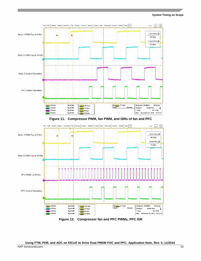
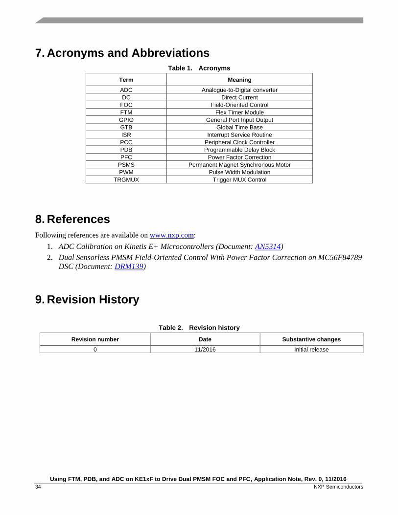
Figure 10, Figure 11, and Figure 12 show the PMW(s) and the control calculations of compressor, fan
and PFC.
NOTE
The PFC control calculation interrupt has the highest priority therefore it
interrupts the other motor calculation interrupts. The compressor (motor 1)
control calculation interrupt has the lowest priority so the duration shown
in the figure has to subtract the time of fan and PFC calculations.
Figure 10. Compressor PWM and ISRs of compressor, fan, and PFC
System Timing on Scope
Using FTM, PDB, and ADC on KE1xF to Drive Dual PMSM FOC and PFC, Application Note, Rev. 0, 11/2016
NXP Semiconductors 33
Figure 11. Compressor PWM, fan PWM, and ISRs of fan and PFC
Figure 12. Compressor fan and PFC PWMs, PFC ISR
Using FTM, PDB, and ADC on KE1xF to Drive Dual PMSM FOC and PFC, Application Note, Rev. 0, 11/2016
34 NXP Semiconductors
7. Acronyms and Abbreviations Table 1. Acronyms
Term Meaning
ADC Analogue-to-Digital converter
DC Direct Current
FOC Field-Oriented Control
FTM Flex Timer Module
GPIO General Port Input Output
GTB Global Time Base
ISR Interrupt Service Routine
PCC Peripheral Clock Controller
PDB Programmable Delay Block
PFC Power Factor Correction
PSMS Permanent Magnet Synchronous Motor
PWM Pulse Width Modulation
TRGMUX Trigger MUX Control
8. References
Following references are available on www.nxp.com:
1. ADC Calibration on Kinetis E+ Microcontrollers (Document: AN5314)
2. Dual Sensorless PMSM Field-Oriented Control With Power Factor Correction on MC56F84789
DSC (Document: DRM139)
9. Revision History
Table 2. Revision history
Revision number Date Substantive changes
0 11/2016 Initial release

Document Number: AN5380 Rev. 0
11/2016
How to Reach Us:
Home Page:
nxp.com
Web Support:
nxp.com/support
Information in this document is provided solely to enable system and software
implementers to use NXP products. There are no express or implied copyright licenses
granted hereunder to design or fabricate any integrated circuits based on the information in
this document. NXP reserves the right to make changes without further notice to any
products herein.
NXP makes no warranty, representation, or guarantee regarding the suitability of its
products for any particular purpose, nor does NXP assume any liability arising out of the
application or use of any product or circuit, and specifically disclaims any and all liability,
including without limitation consequential or incidental damages. “Typical” parameters that
may be provided in NXP data sheets and/or specifications can and do vary in different
applications, and actual performance may vary over time. All operating parameters,
including “typicals,” must be validated for each customer application by customer’s
technical experts. NXP does not convey any license under its patent rights nor the rights of
others. NXP sells products pursuant to standard terms and conditions of sale, which can
be found at the following address: nxp.com/SalesTermsandConditions.
NXP, the NXP logo, NXP SECURE CONNECTIONS FOR A SMARTER WORLD,
Freescale, the Freescale logo, and Kinetis are trademarks of NXP B.V. All other product or
service names are the property of their respective owners.
ARM, the ARM logo, and Cortex are registered trademarks of ARM Limited (or its
subsidiaries) in the EU and/or elsewhere. All rights reserved.
© 2016 NXP B.V.
.