using ldo for led control and brightness matching · important notice for ti reference designs
TRANSCRIPT

TIDU922A – March 2015 – Revised Jul 2015 Using LDO for LED Control and Brightness Matching 1
Copyright © 2015, Texas Instruments Incorporated
TI Designs
Using LDO for LED Control and Brightness Matching
TI Designs
TI Designs provide the foundation that you need including methodology, testing and design files to quickly evaluate and customize the system. TI Designs help you accelerate your time to market.
Design Resources
TIDA-00526 Design Folder
LP38693MPX-ADJ Product Folder
TPD4E1U06 Product Folder
High level Block Diagram
Design Features
Cost optimized LED brightness matching solution
Small foot print with few compensation components
Tunable for a wide range of LED types
Dimmable brightness control feature
Enable/Disable feature
Featured Applications
Battery-power devices
Backlight
Indicator LEDs
Fun-lights for toys Board Image
LDO
MCU/CPU
ON/OFF
EN
Vin VoutBattery
Power Supply
Brand A Brand B Brand C
Ask The Analog Experts
Linear Regulators - Forum
WEBENCH® Design Center
www.ti.com
TIDU922A – March 2015 – Revised Jul 2015 Using LDO for LED Control and Brightness Matching 2
Copyright © 2015, Texas Instruments Incorporated
1 System description This document describes how LDO can be used as a white LED continuous current source for consistent brightness. This design provides higher power efficiency and brightness matching than discrete solutions. All of this in an affordable, small foot print, and easy to implement design.
1.1 Design Overview
In todays market there is a wide range of applications that utilize white light emitting diodes (LED) for illumination, indication, decoration and many other applications. A known issue with white LEDs is that their I-V characteristics fluctuate from brand to brand and part to part. The variation in the current drawn by the LED is directly proportional with the luminous intensity or millicandela (mcd), which is the standard unit to measure brightness intensity. Having various LED suppliers and variation in the manufacturing process make it difficult to obtain consistent and satisfactory results using just a limiting resistor. If a passive circuitry is implemented the limiting resistor will have to be adjusted for each LED. Brightness mismatch could be perceived by customers or users as a poorly made design. This issue can be avoided by implementing a constant current source to each LED using a lightning management unit like LP3952, however if the application requires to power multiple LEDs and cost is an obstacle a low cost, low dropout linear regulator like LP38693-ADJ can be implemented as a current controlled source which will do an excellent job of matching the brightness of the LEDs and controlling the light intensity. This TI design provides all the design files and supporting documentation (schematic, layout, and test data).
1.2 Benefits
If cost is of great concern and the application is sensitive to noise created by power switchers a low noise, low cost, easy to implement low dropout linear (LDO) regulator is a great solution. LDOs offer a consistent current supply for color and brightness accuracy over the manufacturing life of the device. Furthermore, it will provide the following extra features to the system:
High load/line transient regulation and high power supply rejection minimizes noise from source power.
Small foot print with no need of bulk components like inductors or external FETs.
Adjustable LDO output gives flexibility to tune the design for various types of LEDs.
Enable/Disable capability will prolong battery operation.
High current and low IQ maximizes battery life.
Brightness dimming control via PWM.
Fold-back current limiting.

www.ti.com
TIDU922A – March 2015 – Revised Jul 2015 Using LDO for LED Control and Brightness Matching 3
Copyright © 2015, Texas Instruments Incorporated
2 Block Diagram
LP38693MPX-
ADJ
LDO
PWM signal
ON/OFF
EN
Vin
VoutBattery
Power Supply
5V-10V
Brand A Brand B Brand C
ADJ
R R R
TPD4E1U06
ESD protection
Figure 1 Functional block diagram
3 Component Selection This LED brightness matching design features the following parts:
LP38693MPX-ADJ : 500mA Low Dropout CMOS Linear Regulators with Adjustable Output Stable with Ceramic Output Cap.
TPD4E1U06: Quad Channel High Speed ESD Protection Device
LEDs: 3.5V Forward voltage white LEDs
3.1 LP38693MPX-ADJ
The LP38691/3-ADJ low dropout CMOS linear regulators provide 2.0% precision reference voltage, extremely low dropout voltage (250mV @ 500mA load current, VOUT = 5V) and excellent AC performance utilizing ultra low ESR ceramic output capacitors. The low thermal resistance of the WSON and SOT-223 packages allows the full operating current to be used even in high ambient temperature environments. The use of a PMOS power transistor means that no DC base drive current is required to bias it allowing ground pin current to remain below 100 µA regardless of load current, input voltage, or operating temperature. Alternative Adjustable output power LDOs:
LP2951 (ADJ) not functional equivalent - wider Vin/Vout
LP38501-ADJ not functional equivalent - Higher current supply
LP38691-ADJ equivalent functionality -not enable/disable capability For more alternatives visit ti.com/LDO

www.ti.com
TIDU922A – March 2015 – Revised Jul 2015 Using LDO for LED Control and Brightness Matching 4
Copyright © 2015, Texas Instruments Incorporated
3.2 TPD4E1U06
The TPD4E1U06 is a quad channel unidirectional Transient Voltage Suppressor (TVS) based Electrostatic Discharge (ESD) protection diode with ultra low capacitance. This device can dissipate ESD strikes above the maximum level specified by the IEC 61000-4-2 international standard. Features ultra low leakage current of 10nA (max). Its 0.8-pF line capacitance makes it suitable for a wide range of applications.
Figure 2 TPD4E1U06 Block Diagram
3.3 LEDs
The LEDs chosen for this design are from leading LED manufacturers. If more affordable LEDs from other manufactures are used then the brightness mismatch might be grater if they are driven with a passive circuitry.
LED Brand A 3.3.1
Brand: LUMEX Reference number AND720HW
Table 1 LED Brand A
CHARACTERISTICS SYMBOL RATING TYPICAL UNIT
Forward Current IF 20 mA
Forward Voltage VR 3.5 V
Package Type Thru-Hole T1-3/4 5 mm
Luminous Intensity LI 9000 mcd
LED Brand B 3.3.2
Brand: AND Reference number SSL-LX5093UWC/G
Table 2 LED Brand B
CHARACTERISTICS SYMBOL RATING TYPICAL UNIT
Forward Current IF 20 mA
Forward Voltage VR 3.5 V
Package Type Thru-Hole T1-3/4 5 mm
Luminous Intensity LI 11000 mcd

www.ti.com
TIDU922A – March 2015 – Revised Jul 2015 Using LDO for LED Control and Brightness Matching 5
Copyright © 2015, Texas Instruments Incorporated
4 System Design Considerations and component selection In order to have a consistent forward current (IF) across the set of LEDs the LP38693-ADJ LDO is used in a current regulation mode, dependent on one of the LEDs forward voltage drop. The LDO will source current to compensate for the forward voltage across the reference LED. This will allow the other non-matching LEDs connected in parallel to have a constant current flow equal to the reference LED forward current (FI). This design drives eight LEDs four from brand A and four from brand B, their datasheet specifies a forward voltage drop of 3.5V at 20mA. The LP38693-ADJ is able to drive up to 24 LEDs at 20mA per LED The design considerations on this section apply to the given parameters. If your design requires other parameters than the stated in this document, it is necessary to review the ratings on the datasheet of mentioned devices or consider using an alternative part from section 3 or perform an easy parametric search at www.ti.com/ldo
Table 3 Design Parameters
DESIGN PARAMETERS VALUE
Input voltage 5.2V to 10V
Output voltage 5V
Maximum output current 500 mA
White LED forward voltage 3.5V
4.1 Input Voltage Considerations
The input voltage should be higher than the combine voltage of LDO dropout voltage (250mV), LED voltage drop and LED reference voltage (explained in section 4.3.1). Minimum input voltage = VDO +VLED+VLED_REF = 250mV+ 3.5V + 1.49V = 5.2V An input capacitor of at least 1μF is required (ceramic recommended). The capacitor must be located not more than one centimeter from the input pin and returned to a clean analog ground.
www.ti.com
TIDU922A – March 2015 – Revised Jul 2015 Using LDO for LED Control and Brightness Matching 6
Copyright © 2015, Texas Instruments Incorporated
4.2 Capacitor selection consideration
Input output capacitors are necessary for loop stability and eliminate high frequency noise; the following recommendations were taken into account:
To ensure tolerance and variation with temperature X7R or X5R ceramic capacitors were used Input/output caps must be located less than 1cm from the input/output pins
± 20% tolerance of nominal over full operating ratings Output capacitor ESR must not exceed 100mΩ
Output minimum capacitance of 1 µF Input minimum capacitance of 1 µF
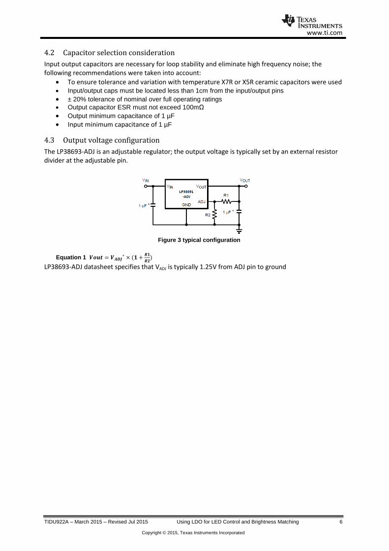
4.3 Output voltage configuration
The LP38693-ADJ is an adjustable regulator; the output voltage is typically set by an external resistor divider at the adjustable pin.
Figure 3 typical configuration
Equation 1 𝑽𝒐𝒖𝒕 = 𝑽𝑨𝑫𝑱∗ × (𝟏 +
𝑹𝟏
𝑹𝟐)
LP38693-ADJ datasheet specifies that VADJ is typically 1.25V from ADJ pin to ground

www.ti.com
TIDU922A – March 2015 – Revised Jul 2015 Using LDO for LED Control and Brightness Matching 7
Copyright © 2015, Texas Instruments Incorporated
The typical model of setting the output voltage could not used in this design, because in order to match the brightness of the array of LEDs the LDO needs to monitor the forward current of one of the LEDs (Reference LED). Various circuit configurations were assessed; the top two configurations were evaluated using the LP38693-ADJ low dropout regulator. Circuit configuration A
Figure 4 Circuit Configuration A
PROS: Requires lower input voltage; the voltage divider at the ADJ pin permits a lower voltage drop at the biasing resistor R3 in this case. CONS: In this case the LP38693 takes more time to reach steady state and the output voltage accuracy is affected by minimal changes in the LED (i.e. LED rising temperature due to prolonged operation). This approach works with most LDO architectures; however, it is recommended to check for stability before implementing design topology

www.ti.com
TIDU922A – March 2015 – Revised Jul 2015 Using LDO for LED Control and Brightness Matching 8
Copyright © 2015, Texas Instruments Incorporated
Circuit configuration B
Figure 5 Circuit Configuration B
PROS: The LDO reaches steady state faster than configuration A, and delivers a superior current matching among all the LEDs. CONS: Due to a higher voltage drop across R3 it requires higher input voltage than circuit B. Next section will explain how to calculate the resistor values on configuration B.

www.ti.com
TIDU922A – March 2015 – Revised Jul 2015 Using LDO for LED Control and Brightness Matching 9
Copyright © 2015, Texas Instruments Incorporated
Resistor value selection 4.3.1
LDO automatically adjust the output voltage to compensate for the voltage drop on the LED. The resistive network has to be adjusted to regulate the forward current of the LED. Resistor R1, R2 and R3 on Figure 5 determine the current across the LED. As a conservative approach 12KΩ was selected for R2 in order to meet the minimum load current requirement of 100uA; a maximum Ohmic value of 100kΩ is recommended for R2. The voltage across R3 will define the LED current; a 100Ω was selected to simplify the calculations. An Ohmic value for R1 was calculated such as 2 volts are delivered across R3. Equation 2 was used to determine the Ohmic value for R1.
Equation 2 𝑹𝟏 = (𝟐
𝑽𝑨𝑫𝑱− 𝟏) × 𝑹𝟐 = (
𝟐
𝟏.𝟐𝟓− 𝟏) × 𝟏𝟐𝒌𝜴 = 𝟕. 𝟐𝒌𝜴
VADJ: The datasheet specifies that The LDO develops a 1.25V reference voltage between the adjustable pin and ground (VADJ varies for other LDOs architectures).
Table 4 LDO Feedback network values
COMPONENT VALUE (SMD-0603 1% STANDARD)
R1 7.32KΩ
R2 12kΩ
R3 100Ω
4.4 Safety
If the final product is intended to have the LEDs exposed to any possible source of electro static discharge (ESD), it is recommended to implement a voltage transient suppressor. The overvoltage and over current transients could totally damage the LEDs or it might permanent disturb their normal functionality. The TPD4E1U06 with its low clamping voltage, ultra low leakage current, and tiny foot print makes it a great safety solution to avid failure due to ESD. The ESD protection was not implemented in the evaluation module. To implement in your design just follow the following guidelines:
The optimum placement is as close to the connector as possible. – EMI during an ESD event can couple from the trace being struck to other nearby
unprotected traces, resulting in early system failures. – The PCB designer needs to minimize the possibility of EMI coupling by keeping any
unprotected traces away from the protected traces which are between the TVS and the connector.
Route the protected traces as straight as possible.
Eliminate any sharp corners on the protected traces between the TVS and the connector by using rounded corners with the largest radii possible.
– Electric fields tend to build up on corners, increasing EMI coupling.

www.ti.com
TIDU922A – March 2015 – Revised Jul 2015 Using LDO for LED Control and Brightness Matching 10
Copyright © 2015, Texas Instruments Incorporated
5 Test setup and results
5.1 Passive circuit vs LDO constant current supply
Since LED brightness intensity is directly dependent on how much current it draws, we measured the voltage across the limiting resistor and calculated the current through the LEDs. Two test setups were made to quantify the benefits of using and LDO over a fix bias voltage with a limiting resistor: The first setup used a fix voltage supply and a simple limiting resistor to limit the current drawn by the array of eight LEDs. The second setup used the same array of eight LEDs, but in this case the current through the LEDs was regulated by a LDO. Then the results from the two scenarios were compared to determine which setup yield a better LED current matching. A tighter LED current matching means that the brightness intensity will be better matched among the array of LEDs.
Table 5 Test Equipment
EQUIPMENT DEVICE NUMBER FUNCTION
Voltage supply Agilent E3631A Constant voltage supply 5.2VDC
For uniformity consistent power supply was used instead of a battery.
Digital Voltmeter
Agilent 34401A Used to measure voltage across the limiting resistor in order to calculate the LED forward current

www.ti.com
TIDU922A – March 2015 – Revised Jul 2015 Using LDO for LED Control and Brightness Matching 11
Copyright © 2015, Texas Instruments Incorporated
Passive circuit test setup and results 5.1.1
From the information on the datasheet of the LEDs we take the assumption that the typical forward voltage (LEDVF) is 3.5V at 20mA. Taking 3.5V as reference the required limiting resistance (RLIM) was calculated with Equation 3.
Equation 3 𝑹𝑳𝑰𝑴=𝑷𝒐𝒘𝒆𝒓𝑺𝒖𝒑𝒑𝒍𝒚𝒗𝒐𝒍𝒕𝒂𝒈𝒆−𝑳𝑬𝑫𝑽𝑭
𝑳𝑬𝑫𝑰𝑭=
𝟓.𝟐𝑽−𝟑.𝟓𝑽
𝟐𝟎𝒎𝑨= 𝟖𝟓𝜴
Four LEDs from brand A and four LEDs from brand B were connected in parallel from the continuous voltage source.
Brand A
x4
Brand B
x4
Rlim Rlim
Power Supply
5.2V
+ +
-
+
Figure 6 Test Setup - limiting resistor
The LED forward current on Table 6 and Table 7 was calculated by measuring the voltage across the limiting resistor and using ohms law to calculate the LED forward current.
Table 6 Limiting resistor Test results
LED Brand
#umber
Limiting resistor [Ω]
Voltage across RLIM [Volts]
LED forward current [mA]
Average Standard deviation
A#1 82 1.98 24.09 24.05
0.38
A#2 82 2.02 24.59
A#3 82 1.95 23.80
A#4 82 1.95 23.74
B#1 82 1.87 22.78 22.96
0.29
B#2 82 1.87 22.80
B#3 82 1.87 22.85
B#4 82 1.92 23.39
Standard Deviation 0.776
Average 0.34
The total input current for the passive circuit was 189mA and the input voltage was 5.2V, which yields a total input power of 982.8mW

www.ti.com
TIDU922A – March 2015 – Revised Jul 2015 Using LDO for LED Control and Brightness Matching 12
Copyright © 2015, Texas Instruments Incorporated
LDO constant current supply – test setup and results 5.1.2
Figure 7 represents the test setup for the constant current supply circuit. All the resistor values were calculated using the equations in section 4.3.1. It was assume that the forward voltage of the LEDs is 3.5V at a 20mA forward current.
LP38693MPX-
ADJ
LDO
EN
Vin
Vout
Power Supply
5.2V
Brand B
X1
Brand B
x3
Brand C
x4
ADJ
100Ω
100Ω 100Ω
12kΩ
7.32kΩ
-
+
Figure 7 Test setup – LDO Current source
Table 7 LDO Constant current supply - test results
LED BRAND #NUMBER
LIMITING RESISTOR [Ω]
VOLTAGE ACROSS RLIM
[VOLTS]
LED FORWARD CURRENT
[MA]
AVERAGE STANDARD DEVIATION
A#1 100 1.99 19.91 19.87
0.33
A#2 100 2.03 20.3
A#3 100 1.97 19.74
A#4 100 1.95 19.52
B#1 100 1.91 19.13 19.25
0.22
B#2 100 1.91 19.13
B#3 100 1.92 19.16
B#4 100 1.96 19.57
Standard Deviation 0.438
Average 0.27
The total input current of the LDO is 159mA and the input voltage is 5.2V, which yields a total input power of 826.8mW

www.ti.com
TIDU922A – March 2015 – Revised Jul 2015 Using LDO for LED Control and Brightness Matching 13
Copyright © 2015, Texas Instruments Incorporated
Comparison 5.1.3
By comparing Table 6 and Table 7 we can conclude the following advantages of using LDO over passive circuitry:
Brand to brand current matching improved by 43.5%
Within brand current matching improvement of 20%
LDO is more accurate at delivering the desired LED forward current of 20mA. Passive circuitry delivered an average of 23.51mA when the LDO did a better job with an average of 19.56mA forward current per LED.
The LDO prolongs battery operation by using 156mW less than the passive circuit approach. LDO total input power = VIN x IIN = 5.2V X 63mA = 826.8mW Passive circuit total input power =VIN x IIN = 5.2V X 91mA = 982.8mW
Brand to Brand matching
pasive components 0.78
LDO 0.44
Passive Circuitry
LDO
0.00
0.10
0.20
0.30
0.40
0.50
0.60
0.70
0.80
0.90
LED
fo
rwar
d c
urr
en
t d
evi
atio
n 43.5%
improvement
whitin brand matching
pasive components 0.34
LDO 0.27
Passive Circuitry
LDO
-
0.05
0.10
0.15
0.20
0.25
0.30
0.35
0.40
LED
fo
rwar
d c
urr
en
t d
evi
atio
n
20% improvement

www.ti.com
TIDU922A – March 2015 – Revised Jul 2015 Using LDO for LED Control and Brightness Matching 14
Copyright © 2015, Texas Instruments Incorporated
5.2 Dimmable brightness
This test demonstrates the ability of dimming LED brightness by applying a PWM signal at the enable pin of the LDO. This dimmable ability is directly related with the architecture design of the enable feature it is necessary to verify functionality on the bench if other LDO, PWM frequency, or PWM voltage is intended to be used for a similar design. The signal at the enable pin must not go lower than ground potential or higher than Vin. The enable pin has no internal pull-up or pull-down, it must never be left floating otherwise it will have an undetermined behavior.
Table 8 Equipment used in dimmable brightness test
A square signal with variable duty cycle was applied to the enable pin of the LP38693-ADJ.Figure 8 represents the dimmable brightness test setup, the feedback network components were calculated using the equation in section 4.3.1
LP38693MPX-ADJLDO
EN
Vin
VoutPower Supply
5.2V
Power Supply
5.2V
Brand B X1
Brand B X1
Brand B x3
Brand B x3
Brand C x4
Brand C x4
ADJ
100Ω
100Ω 100Ω
12kΩ
7.32kΩ
Square wave
generator
Figure 8 Dimmable brightness test setup
The LED brightness softens when the current through the LED drops. Table 9 shows how the LEDs forward
current drops by adjusting the duty cycle of the input signal on the enable pin.
Table 9 Dimmable Brightness Test Results
DUTY CYCLE VOLTAGE ACROSS RLIM [VOLTS] LED FORWARD CURRENT
[AMPS]
20% 60mV 0.6 mA
50% 112mV 1.12mA
80% 1.06V 10.6mA
TEST EQUIPMENT PART NUMBER FUNCTION
Oscilloscope Agilent MSO7034B Measure the waveform signals of the system
Voltage supply Agilent E3631A Supply DC voltage
Function generator (square signal generator)
Agilent 33220A Signal: Square wave Frequency: 1KHz High level: 2.5 Low level: 0V Duty cycle: 20% - 80%

www.ti.com
TIDU922A – March 2015 – Revised Jul 2015 Using LDO for LED Control and Brightness Matching 15
Copyright © 2015, Texas Instruments Incorporated
Brightness is directly related with LED forward current. Table 10 shows a comparison between the pulsed output voltage charging and discharging the output cap and LED brightness. Test setup: DC coupled probe capture waveform at VOUT PIN Time division: 2ms\DIV time division Voltage: 2V\DIV
Table 10 Dimmable Brightness Comparison Test Results (Part 2)
SCOPE SHOTS AT VOUT PIN
BOARD PICTURE
SQ-Wave Duty Cycle = 20%
SQ-Wave Duty Cycle = 50%
SQ-Wave Duty Cycle = 80%

www.ti.com
TIDU922A – March 2015 – Revised Jul 2015 Using LDO for LED Control and Brightness Matching 16
Copyright © 2015, Texas Instruments Incorporated
6 Design Files
6.1 Schematics
To download the Schematics for each board, see the design files at http://www.ti.com/tool/TIDA-00526
Figure 9: Schematic
www.ti.com
TIDU922A – March 2015 – Revised Jul 2015 Using LDO for LED Control and Brightness Matching 17
Copyright © 2015, Texas Instruments Incorporated
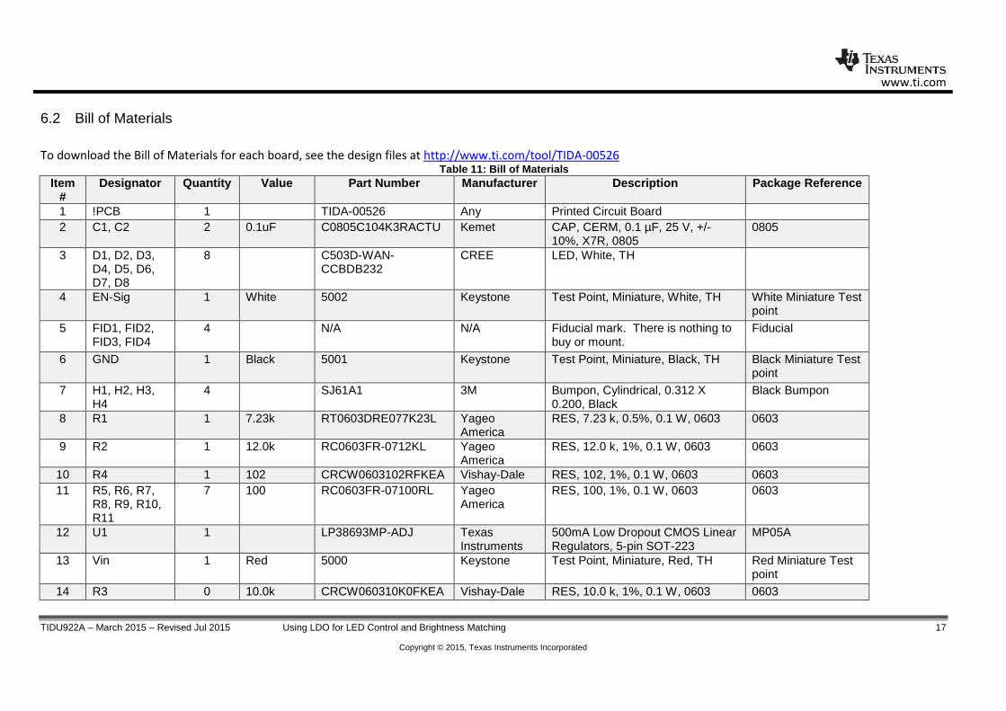
6.2 Bill of Materials
To download the Bill of Materials for each board, see the design files at http://www.ti.com/tool/TIDA-00526
Table 11: Bill of Materials
Item #
Designator Quantity Value Part Number Manufacturer Description Package Reference
1 !PCB 1 TIDA-00526 Any Printed Circuit Board
2 C1, C2 2 0.1uF C0805C104K3RACTU Kemet CAP, CERM, 0.1 µF, 25 V, +/- 10%, X7R, 0805
0805
3 D1, D2, D3, D4, D5, D6, D7, D8
8 C503D-WAN-CCBDB232
CREE LED, White, TH
4 EN-Sig 1 White 5002 Keystone Test Point, Miniature, White, TH White Miniature Test point
5 FID1, FID2, FID3, FID4
4 N/A N/A Fiducial mark. There is nothing to buy or mount.
Fiducial
6 GND 1 Black 5001 Keystone Test Point, Miniature, Black, TH Black Miniature Test point
7 H1, H2, H3, H4
4 SJ61A1 3M Bumpon, Cylindrical, 0.312 X 0.200, Black
Black Bumpon
8 R1 1 7.23k RT0603DRE077K23L Yageo America
RES, 7.23 k, 0.5%, 0.1 W, 0603 0603
9 R2 1 12.0k RC0603FR-0712KL Yageo America
RES, 12.0 k, 1%, 0.1 W, 0603 0603
10 R4 1 102 CRCW0603102RFKEA Vishay-Dale RES, 102, 1%, 0.1 W, 0603 0603
11 R5, R6, R7, R8, R9, R10, R11
7 100 RC0603FR-07100RL Yageo America
RES, 100, 1%, 0.1 W, 0603 0603
12 U1 1 LP38693MP-ADJ Texas Instruments
500mA Low Dropout CMOS Linear Regulators, 5-pin SOT-223
MP05A
13 Vin 1 Red 5000 Keystone Test Point, Miniature, Red, TH Red Miniature Test point
14 R3 0 10.0k CRCW060310K0FKEA Vishay-Dale RES, 10.0 k, 1%, 0.1 W, 0603 0603

www.ti.com
TIDU922A – March 2015 – Revised Jul 2015 Using LDO for LED Control and Brightness Matching 18
Copyright © 2015, Texas Instruments Incorporated
Layout Prints 6.2.1
To download the Layout Prints for each board, see the design files at http://www.ti.com/tool/TIDA-00526
Figure 10 Top Silkscreen
TOP SOLDER MASK
Figure 11 Top Solder Mask
TOP LAYER
Figure 12 Top Layer
BOTTOM LAYER
Figure 13 Bottom Layer
www.ti.com
TIDU922A – March 2015 – Revised Jul 2015 Using LDO for LED Control and Brightness Matching 19
Copyright © 2015, Texas Instruments Incorporated
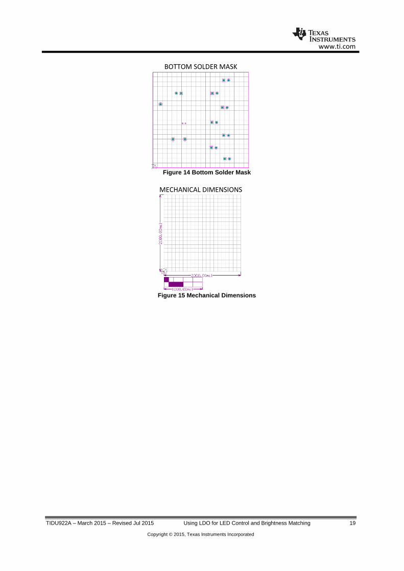
BOTTOM SOLDER MASK
Figure 14 Bottom Solder Mask
MECHANICAL DIMENSIONS
Figure 15 Mechanical Dimensions

www.ti.com
TIDU922A – March 2015 – Revised Jul 2015 Using LDO for LED Control and Brightness Matching 20
Copyright © 2015, Texas Instruments Incorporated
6.3 Altium Designer Project
To download the Altium project files for each board, see the design files at http://www.ti.com/tool/TIDA-00526
Figure 16 Altium Screenshot

www.ti.com
TIDU922A – March 2015 – Revised Jul 2015 Using LDO for LED Control and Brightness Matching 21
Copyright © 2015, Texas Instruments Incorporated
6.4 Layout Guidelines
Figure 17 Layout hints

www.ti.com
TIDU922A – March 2015 – Revised Jul 2015 Using LDO for LED Control and Brightness Matching 22
Copyright © 2015, Texas Instruments Incorporated
6.5 Gerber files
To download the Gerber files for each board, see the design files at http://www.ti.com/tool/TIDA-00526
Figure 18 CAMtastic.CAM Gerber view

www.ti.com
TIDU922A – March 2015 – Revised Jul 2015 Using LDO for LED Control and Brightness Matching 23
Copyright © 2015, Texas Instruments Incorporated
6.6 Assembly Drawings
To download the Assembly Drawings for each board, see the design files at http://www.ti.com/tool/TIDA-00526
Figure 19 Top Assembly Drawings

www.ti.com
TIDU922A – March 2015 – Revised Jul 2015 Using LDO for LED Control and Brightness Matching 24
Copyright © 2015, Texas Instruments Incorporated
7 About the Author Antony Pierre Carvajales Is an Applications Engineer on the mobile power devices RF power group at Texas Instruments. Antony has worked in various business units expanding his knowledge on analog circuitry to help customers solve their design challenges using TI technologies.

IMPORTANT NOTICE FOR TI REFERENCE DESIGNS
Texas Instruments Incorporated ("TI") reference designs are solely intended to assist designers (“Buyers”) who are developing systems thatincorporate TI semiconductor products (also referred to herein as “components”). Buyer understands and agrees that Buyer remainsresponsible for using its independent analysis, evaluation and judgment in designing Buyer’s systems and products.TI reference designs have been created using standard laboratory conditions and engineering practices. TI has not conducted anytesting other than that specifically described in the published documentation for a particular reference design. TI may makecorrections, enhancements, improvements and other changes to its reference designs.Buyers are authorized to use TI reference designs with the TI component(s) identified in each particular reference design and to modify thereference design in the development of their end products. HOWEVER, NO OTHER LICENSE, EXPRESS OR IMPLIED, BY ESTOPPELOR OTHERWISE TO ANY OTHER TI INTELLECTUAL PROPERTY RIGHT, AND NO LICENSE TO ANY THIRD PARTY TECHNOLOGYOR INTELLECTUAL PROPERTY RIGHT, IS GRANTED HEREIN, including but not limited to any patent right, copyright, mask work right,or other intellectual property right relating to any combination, machine, or process in which TI components or services are used.Information published by TI regarding third-party products or services does not constitute a license to use such products or services, or awarranty or endorsement thereof. Use of such information may require a license from a third party under the patents or other intellectualproperty of the third party, or a license from TI under the patents or other intellectual property of TI.TI REFERENCE DESIGNS ARE PROVIDED "AS IS". TI MAKES NO WARRANTIES OR REPRESENTATIONS WITH REGARD TO THEREFERENCE DESIGNS OR USE OF THE REFERENCE DESIGNS, EXPRESS, IMPLIED OR STATUTORY, INCLUDING ACCURACY ORCOMPLETENESS. TI DISCLAIMS ANY WARRANTY OF TITLE AND ANY IMPLIED WARRANTIES OF MERCHANTABILITY, FITNESSFOR A PARTICULAR PURPOSE, QUIET ENJOYMENT, QUIET POSSESSION, AND NON-INFRINGEMENT OF ANY THIRD PARTYINTELLECTUAL PROPERTY RIGHTS WITH REGARD TO TI REFERENCE DESIGNS OR USE THEREOF. TI SHALL NOT BE LIABLEFOR AND SHALL NOT DEFEND OR INDEMNIFY BUYERS AGAINST ANY THIRD PARTY INFRINGEMENT CLAIM THAT RELATES TOOR IS BASED ON A COMBINATION OF COMPONENTS PROVIDED IN A TI REFERENCE DESIGN. IN NO EVENT SHALL TI BELIABLE FOR ANY ACTUAL, SPECIAL, INCIDENTAL, CONSEQUENTIAL OR INDIRECT DAMAGES, HOWEVER CAUSED, ON ANYTHEORY OF LIABILITY AND WHETHER OR NOT TI HAS BEEN ADVISED OF THE POSSIBILITY OF SUCH DAMAGES, ARISING INANY WAY OUT OF TI REFERENCE DESIGNS OR BUYER’S USE OF TI REFERENCE DESIGNS.TI reserves the right to make corrections, enhancements, improvements and other changes to its semiconductor products and services perJESD46, latest issue, and to discontinue any product or service per JESD48, latest issue. Buyers should obtain the latest relevantinformation before placing orders and should verify that such information is current and complete. All semiconductor products are soldsubject to TI’s terms and conditions of sale supplied at the time of order acknowledgment.TI warrants performance of its components to the specifications applicable at the time of sale, in accordance with the warranty in TI’s termsand conditions of sale of semiconductor products. Testing and other quality control techniques for TI components are used to the extent TIdeems necessary to support this warranty. Except where mandated by applicable law, testing of all parameters of each component is notnecessarily performed.TI assumes no liability for applications assistance or the design of Buyers’ products. Buyers are responsible for their products andapplications using TI components. To minimize the risks associated with Buyers’ products and applications, Buyers should provideadequate design and operating safeguards.Reproduction of significant portions of TI information in TI data books, data sheets or reference designs is permissible only if reproduction iswithout alteration and is accompanied by all associated warranties, conditions, limitations, and notices. TI is not responsible or liable forsuch altered documentation. Information of third parties may be subject to additional restrictions.Buyer acknowledges and agrees that it is solely responsible for compliance with all legal, regulatory and safety-related requirementsconcerning its products, and any use of TI components in its applications, notwithstanding any applications-related information or supportthat may be provided by TI. Buyer represents and agrees that it has all the necessary expertise to create and implement safeguards thatanticipate dangerous failures, monitor failures and their consequences, lessen the likelihood of dangerous failures and take appropriateremedial actions. Buyer will fully indemnify TI and its representatives against any damages arising out of the use of any TI components inBuyer’s safety-critical applications.In some cases, TI components may be promoted specifically to facilitate safety-related applications. With such components, TI’s goal is tohelp enable customers to design and create their own end-product solutions that meet applicable functional safety standards andrequirements. Nonetheless, such components are subject to these terms.No TI components are authorized for use in FDA Class III (or similar life-critical medical equipment) unless authorized officers of the partieshave executed an agreement specifically governing such use.Only those TI components that TI has specifically designated as military grade or “enhanced plastic” are designed and intended for use inmilitary/aerospace applications or environments. Buyer acknowledges and agrees that any military or aerospace use of TI components thathave not been so designated is solely at Buyer's risk, and Buyer is solely responsible for compliance with all legal and regulatoryrequirements in connection with such use.TI has specifically designated certain components as meeting ISO/TS16949 requirements, mainly for automotive use. In any case of use ofnon-designated products, TI will not be responsible for any failure to meet ISO/TS16949.IMPORTANT NOTICE
Mailing Address: Texas Instruments, Post Office Box 655303, Dallas, Texas 75265Copyright © 2015, Texas Instruments Incorporated