utmi plus1 0.prn - nxp semiconductors€¦ · page 5 acronyms and terms fs full-speed hs high-speed...
TRANSCRIPT

UTMI+ Specification, Revision 1.0, February 25th , 2004
Page 1
UTMI+ Specification
Revision 1.0

UTMI+ Specification, Revision 1.0, February 25th , 2004
Page 2
Revision History
Revision Issue Date Comment 0.7 April 24th, 2002 Initial version 0.71 April 29th, 2002 Reworked the different levels 0.72 June 4th, 2002 Extended definition of OpMode
Added outline on how to implement multi-port host controllers using UTMI+
0.8 June 17th, 2002 Promoted to version 0.8 to allow review by OTG workgroup members 0.81 July 3rd, 2002 Clarified Optional charge pump, rewording for grammer and clarity 0.82 July 22nd, 2002 Added signal IdPullup
Added signal FsSerialMode and legacy interface signals Added signal TxBitstuffEnable / TxBitstuffEnableH Removed signal SessEnd
0.83 October 23rd, 2002 Changed FsSerialMode into FsLsSerialMode Added SessEnd signal back because there is still uncertainty that an OTG system will work without this signal in all conditions. Added clarifications
0.9rc January 8th, 2003 Added clarification of long EOP generation Modified suspend/resume behaviour in host mode Changed IdPullup timing Added chapter on T&MT connector
0.9rc2 January 17th, 2003 Added section on ambiguities in UTMI v1.05 spec Added clarification on HostDisconnect signal when PHY is in suspend
0.9rc3 February 7th, 2003 Changed TermSelect definition for LS devices Changed clarification for RxActive/RxValid during transmit Added clarification for LineState
0.9 February 21st, 2003 Added more clarification to LineState Promoted to version 0.9 by OTG workgroup
0.91 October 13th, 2003 Changed time between IdPullup being asserted and IdDig having a valid value. Updated LineState tables Changed behaviour of OpMode during chirp sequence Updated disclaimer
0.92 November 13th, 2003 Changed time T1 during resume to be minimum 16 LS bit times. This allows the transceiver to complete the resume signaling in a correct way.
1.0 February 25th, 2004 Version approved by the Promoters and Adopters of UTMI+/ULPI "The present Specification has been circulated for the sole benefit of legally-recognized Promoters, Adopters and Contributors of the Specification. All rights are expressly reserved, including but not limited to intellectual property rights under patents, trademarks, copyrights and trade secrets. The respective Promoter's, Adopter's

UTMI+ Specification, Revision 1.0, February 25th , 2004
Page 3
or Contributor's agreement entered into by Promoters, Adopters and Contributors sets forth their conditions of use of the Specification."
Table of Contents
1. Introduction.................................................................................................................................6 1.1 Purpose..................................................................................................................................6 1.2 Audience................................................................................................................................6 1.3 Disclaimers.............................................................................................................................6 1.4 Relevant Documents................................................................................................................6
2. Definition of Different levels........................................................................................................7 2.1 UTMI+ level 0 : USB2.0 peripherals ...........................................................................................7
2.1.1 Additional requirements and clarifications on top of UTMI ................................................8 2.2 UTMI+ level 1 : USB2.0 peripherals, host controllers and On-the-Go devices (HS and FS only)......9
2.2.1 Additional signals for UTMI+ level 1. ..............................................................................9 2.2.2 Generation of long EOP ............................................................................................. 15 2.2.3 Data line pulsing........................................................................................................ 16 2.2.4 HS keep-alive generation............................................................................................ 16 2.2.5 UTMI+ level 1 transceiver core used in a USB2.0 peripheral........................................... 17
2.3 UTMI+ level 2 : USB2.0 peripherals, host controllers and On-the-Go devices (HS / FS / LS / no hub support)...................................................................................................................................... 17
2.3.1 XcvrSelect(1:0) .......................................................................................................... 18 2.3.2 LS keep-alive generation ............................................................................................ 19 2.3.3 LineState.................................................................................................................. 19
2.4 UTMI+ level 3 : USB2.0 peripherals, host controllers and On-the-Go devices (HS / FS / LS / preamble) 20
2.4.1 XcvrSelect(1:0) .......................................................................................................... 20 2.4.2 Multi-port host controllers ........................................................................................... 21
3. Explanation of different signaling modes................................................................................. 22 3.1 Chirp sequence..................................................................................................................... 22 3.2 Suspend / Resume signaling for downstream facing ports ......................................................... 22 3.3 Transmit error reporting for downstream facing ports ................................................................. 24 3.4 Selection of different signaling modes for upstream and downstream facing ports ........................ 25
4. T&MT Connector ....................................................................................................................... 26
Figures
Figure 1 : UTMI+ levels ...........................................................................................................................7 Figure 2 : UTMI+ level 0 entity diagram (16-bit interface).............................................................................8 Figure 3 : UTMI+ level 1 entity diagram...................................................................................................10 Figure 4 : HostDisconnect behaviour (signals are not on scale).................................................................14 Figure 5 : Data line pulsing for a Dual-Role B-device ................................................................................16 Figure 6 : HS keep-alive generation ........................................................................................................16 Figure 7 : UTMI+ level 2 entity diagram...................................................................................................18 Figure 8 : LS keep-alive generation.........................................................................................................19

UTMI+ Specification, Revision 1.0, February 25th , 2004
Page 4
Figure 9 : Reset sequence for a HS peripheral connected to a HS Host Controller ......................................22 Figure 10 : Resume signaling on downstream facing ports........................................................................23 Figure 11 : Transmit error reporting for downstream facing ports................................................................24
Tables
Table 1 : Filtering of LineState .................................................................................................................9 Table 2 : UTMI+ level 1 transceiver core used in a USB2.0 peripheral ........................................................17 Table 3 : LineState for upstream facing ports (DpPulldown and DmPulldown = 0)........................................20 Table 4 : LineState for downstream facing ports(DpPulldown and DmPulldown = 1).....................................20 Table 5 : Different signaling modes for upstream and downstream facing ports ...........................................25 Table 6 : T&MT connector pinning[1] ........................................................................................................26

UTMI+ Specification, Revision 1.0, February 25th , 2004
Page 5
Acronyms and Terms FS Full-Speed HS High-Speed IC Integrated Circuit LS Low-Speed OTG On-The-Go SE0 Single Ended Zero USB Universal Serial Bus USB-IF USB Implementers Forum UTMI USB 2.0 Transceiver Macrocell Interface
Contributors Bart Vertenten Philips Srinivas Pattamatta Philips Jerome Tjia Philips Chung Wing Yan Philips Farran Mackay Philips Chris Kolb ARC Christopher Meyers ARC David Cobbs Cypress David Wooten Cypress Eric Huang Synopsys Ravikumar Govindaraman Synopsys Saleem Mohammad Synopsys Michael Pennell SMSC Nabil Takla Innovative Paul Berg MCCI Peter Hirt ST Microelectronics Alok Kaushik ST Microelectronics Rob Douglas Mentor Graphics Andy King Mentor Graphics Zong Liang Wu TransDimension Hemal Doshi Portalplayer Inc

UTMI+ Specification, Revision 1.0, February 25th , 2004
Page 6
1. Introduction 1.1 Purpose The purpose of this document is to specify an interface to which USB 2.0 ASIC, ASSP, discrete PHY, system peripherals and IP vendors can develop USB2.0 products. The existing UTMI specification describes an interface only for USB2.0 peripherals. The UTMI specification can not be used to develop USB 2.0 host or On-The-Go peripherals. The intention of this UTMI+ specification is to extend the UTMI specification to standardize the interface for USB 2.0 hosts and USB 2.0 On-The-Go peripherals. The UTMI+ specification defines and standardizes the interoperability characteristics with existing USB 2.0 hosts and peripherals. 1.2 Audience This document is intended for developers and vendors of USB 2.0 ASIC, ASSP, discrete PHY, system, peripheral and IP products. 1.3 Disclaimers This document is a recommendation of the contributors indicated in the title pages. It does not necessarily reflect the position of their respective companies, the OTG working group, or the position of the USB-IF. 1.4 Relevant Documents
• USB 2.0 Transceiver Macrocell Interface Specification, version 1.05, Steve McGowan, March 29th, 2001 • USB 2.0 Transceiver and Macrocell Tester(T&MT) Interface Specification, Wes Talarek, version 1.2, April 4th,
2001 • On-The-Go Supplement to the USB 2.0 Specification (www.usb.org/developers/onthego) • USB 2.0 Specification (www.usb.org/developers/docs.html) • OTG Certification Specification Revision 0.7 • ECN_27%_ Resistor (www.usb.org/app/members/ecn_html) • OTG Labeling Specification Revision 0.63
UTMI+ Specification, Revision 1.0, February 25th , 2004
Page 7
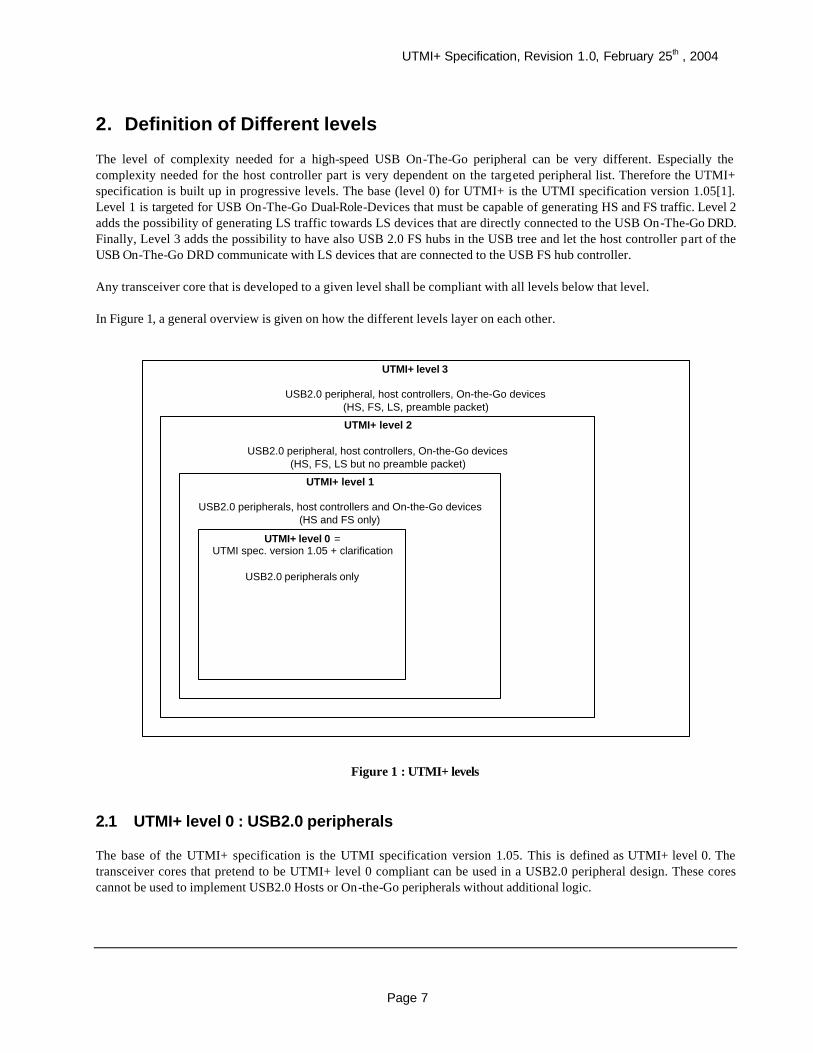
2. Definition of Different levels The level of complexity needed for a high-speed USB On-The-Go peripheral can be very different. Especially the complexity needed for the host controller part is very dependent on the targeted peripheral list. Therefore the UTMI+ specification is built up in progressive levels. The base (level 0) for UTMI+ is the UTMI specification version 1.05[1]. Level 1 is targeted for USB On-The-Go Dual-Role-Devices that must be capable of generating HS and FS traffic. Level 2 adds the possibility of generating LS traffic towards LS devices that are directly connected to the USB On-The-Go DRD. Finally, Level 3 adds the possibility to have also USB 2.0 FS hubs in the USB tree and let the host controller part of the USB On-The-Go DRD communicate with LS devices that are connected to the USB FS hub controller. Any transceiver core that is developed to a given level shall be compliant with all levels below that level. In Figure 1, a general overview is given on how the different levels layer on each other.
UTMI+ level 0 =UTMI spec. version 1.05 + clarification
USB2.0 peripherals only
UTMI+ level 1
USB2.0 peripherals, host controllers and On-the-Go devices(HS and FS only)
UTMI+ level 2
USB2.0 peripheral, host controllers, On-the-Go devices(HS, FS, LS but no preamble packet)
UTMI+ level 3
USB2.0 peripheral, host controllers, On-the-Go devices(HS, FS, LS, preamble packet)
Figure 1 : UTMI+ levels
2.1 UTMI+ level 0 : USB2.0 peripherals The base of the UTMI+ specification is the UTMI specification version 1.05. This is defined as UTMI+ level 0. The transceiver cores that pretend to be UTMI+ level 0 compliant can be used in a USB2.0 peripheral design. These cores cannot be used to implement USB2.0 Hosts or On-the-Go peripherals without additional logic.

UTMI+ Specification, Revision 1.0, February 25th , 2004
Page 8
DataIn(15:8) DataOut(15:8)DataIn(7:0) DataOut(7:0)
TXValid
TXValidH
DataBus16_8
TXReady
RXActive
RXValid
RXValidH
CLKReset
SuspendM
XcvrSelect
TermSelect
RXError
DP
DM
OpMode(1:0) LineState(1:0)
16-bit interface
Figure 2 : UTMI+ level 0 entity diagram (16-bit interface)
During the implementation of UTMI+, it was found that some parts of the UTMI spec were not clearly specified or could be interpreted in different ways. This caused that integration of UTMI transceiver from one vendor with the USB device core from another vendor was not always working. To remove these problems from future designs any core that is UTMI+ compliant must implement the requirements described in section 2.1.1.
For more details on how to implement a UTMI+ level 0 transceiver see also the UTMI spec[1]. In Figure 2 a general overview is given of all interface signals needed for UTMI+ level 0 transceiver with 16-bit interface. For a UTMI+ level 0 transceiver with 8-bit interface the TXValidH, RXValidH, DataBus16_8, DataIn(15:8) and DataOut(15:8) signals are not needed.
2.1.1 Additional requirements and clarifications on top of UTMI 2.1.1.1 Use of LineState for timers The UTMI spec mentions several times that LineState is the most accurate signal to be used for timing a certain state on the USB bus. It is not a hard requirement for the USB device core designer to use this signal. He can use whatever method he wants as long as correct behavior on the USB bus is guaranteed without forcing additional constraints on the PHY design. 2.1.1.2 LineState filtering Minimal filtering should be applied to LineState to ensure that skew on the DP/DM signals does not generate unwanted SE0 or SE1 states between J and K states. For instance, for FS mode Table 7-9 of the USB 2.0 Specification identifies the “Width of SE0 interval during differential transition” to be 14ns max. These SE0 states are noise to the SIE and should

UTMI+ Specification, Revision 1.0, February 25th , 2004
Page 9
not be propagated by LineState. To be able to filter worst case SE0 noise, the transceiver should implement filtering as indicated in Table 1. Filtering should only occur on an SE0. If during filtering the SE0 a non-SE0 event occurs then the filtering should stop and linestate behaviour continues as previously.
Bus speed 8-bit interface (CLK = 60MHz) 16-bit interface (CLK = 30 MHz) Low-speed mode filtering 14 CLK cycles 7 CLK cycles Full-speed mode filtering 2 CLK cycles 1 CLK cycle High-speed mode filtering 2 CLK cycles 1 CLK cycle
Table 1 : Filtering of LineState
2.1.1.3 RxActive/RxValid during transmit The UTMI PHY must internally block the USB receive path once a USB transmit has begun. The receive path can be unblocked when the internal Squelch (HS) or SE0-to-J (FS/LS) is seen. 2.1.1.4 TxReady behavior when not bitstuffing TxReady must be used in chirp mode. If TxReady is not asserted by the UTMI PHY when the USB device core was sending a chirp, it can cause the device core to lock-up if the device core is holding the transmit data on the bus until it sees TxReady asserted. By explicitly requiring that TxReady must be asserted for all transmit data including chirp data, this problem can be avoided. 2.1.1.5 Receive End Delay At the end of page 59 of the UTMI spec v.1.05 there is a contradiction between the number of bit times and the number of clock cycles for Total Receive End Delay for an interface running at 30MHz. 6 30 MHz clock cycles is actually 96 bit times. For a 16 bit transceiver interface, the Total Receive End Delay must be between 32-96 bit times or 2-6, 30 MHz CLKs 2.2 UTMI+ level 1 : USB2.0 peripherals, host controllers and On-the-Go devices (HS
and FS only) Any transceiver core that has an interface compliant with UTMI+ level 1, has all signals compliant with UTMI+ level 0. A transceiver core with UTMI+ level 1 interface can be used for USB2.0 peripheral, host or On-the-Go device designs that support only HS and FS traffic. If a host controller needs to be able to communicate with a LS device some additional functions are required that are not part of level1 (cfr section 2.3). Transceivers implementing level 1 may optionally include an integrated charge pump to supply VBUS current to the On-The-Go connector. If the charge pump is integrated within the transceiver macrocell then a description of the charge pump must be given in the transceiver datasheet to allow integrators to build a complete USB On-The-Go peripheral. If the charge pump is not integrated within the transceiver macrocell then the optional DrvVbus signal may be omitted from the macrocell. 2.2.1 Additional signals for UTMI+ level 1. USB On-The-Go peripherals have some additional capabilities and therefore some new signals need to be implemented. 1. A USB On-The-Go dual role peripheral needs to be capable to distinguish between a mini-A and mini-B plug. 2. A USB On-The-Go peripheral has to know if Vbus is below or above a certain voltage level.

UTMI+ Specification, Revision 1.0, February 25th , 2004
Page 10
3. A USB On-The-Go peripheral must be able to drive Vbus and charge or discharge Vbus. 4. A USB On-The-Go dual role peripheral needs to be able to switch the pull-up resistor on DP and the pull-down
resistor on both DP and DM. 5. The downstream facing port of a host controller must have 15 kOhm pull-down resistors on both DP and DM lines.
Some signals are needed to do the correct switching of the resistors 6. The host controller must be able to detect a disconnect of a peripheral. This is possible for a FS peripheral by using
LineState, but it is not possible for HS peripherals using the current UTMI specification. Therefore an additional signal needs to be implemented. To make the design of the digital SIE easier, this new disconnect signal will be used in both speeds (HS/FS) to indicate if there is a device connected or not.
In Figure 3 an overview is given of all signals needed for the UTMI+ level 1 interface.
DataIn(15:8) DataOut(15:8)
DataIn(7:0) DataOut(7:0)
TXValid
TXValidH
DataBus16_8
TXReady
RXActive
RXValid
RXValidH
CLKReset
SuspendM
XcvrSelect
TermSelect
RXError
DP
DM
OpMode(1:0) LineState(1:0)
16-bit interfaceUTMI+ level 0 entity
16-bit interfaceUTMI+ level 1 entity
HostDisconnect
DpPulldown
DmPulldown
IdDig
AValid
BValid
VbusValid
DrvVbus
ChrgVbus
DischrgVbus
IdPullup
TxBitstuffEnable
Rx_DP
Rx_DM
Rx_RCV
Tx_Enable_N
Tx_DAT
Tx_SE0
FsLsSerialMode
TxBitstuffEnableH
SessEnd
Figure 3 : UTMI+ level 1 entity diagram

UTMI+ Specification, Revision 1.0, February 25th , 2004
Page 11
2.2.1.1 IdDig / IdPullup The id signal is indicating the state of the ID pin on the USB mini receptacle. This pin makes it able to determine which kind of plug is connected. To save power, there is also an IdPullup signal. Only when this IdPullup signal is high, the analog Id line will be sampled and the IdDig signal will indicate the correct value. IdPullup Signal that enables the sampling of the analog Id line.
0b : Sampling of Id pin is disabled. IdDig is not valid 1b : Sampling of Id pin is enabled.
IdDig Indicates whether the connected plug is a mini-A or mini-B. This is only valid when IdPullup is set to 1b. It must be valid within 50ms after IdPullup is set to 1b. 0b : connected plug is a mini-A 1b : connected plug is a mini-B
2.2.1.2 AValid The AValid signal is used to indicate if the session for an A-peripheral is valid. This signal is 1b when Vbus is above 2V. Avalid Indicates if the session for an A-peripheral is valid (0.8V < Vth < 2V).
0b : Vbus < 0.8V 1b : Vbus > 2V
2.2.1.3 BValid The BValid signal is used to indicate if the session for a B-peripheral is valid. This signal is 1b when Vbus is above 4V. Bvalid Indicates if the session for an B-peripheral is valid (0.8V < Vth < 4V).
0b : Vbus < 0.8V 1b : Vbus > 4V
2.2.1.4 VbusValid The VbusValid signal is used to determine whether or not the voltage on Vbus is at a valid level for operation. The minimum threshold for the Vbus comparator is 4.4V VbusValid Indicates if the voltage on Vbus is at a valid level for operation (4.4V < Vth < 4.75V).
0b : Vbus < 4.4V 1b : Vbus > 4.75V
2.2.1.5 SessEnd The SessEnd signal is used to determine if the voltage on Vbus is below its B-Device Session End threshold. SessEnd Indicates if the voltage on Vbus (0.2V < Vth < 0.8V).
1b : Vbus < 0.2V 0b : Vbus > 0.8V
UTMI+ Specification, Revision 1.0, February 25th , 2004
Page 12
According to the definition in the OTG supplement of the USB 2.0 specification, it must be possible to build a USB OTG DRD without the SessEnd signal. The detection can be done in the digital controller section. 50ms after Vbus is discharged, the voltage on Vbus must be below the B-device Session End Threshold. This is correct in a normal working environment. However it is always possible that in systems for some reason the Vbus does not go down to levels less than SessEnd (e.g. standard host, short circuit on the charge pump so that Vbus is always on, etc). Therefore it is seen that this signal is a must and is preferred to be used in order to have a correct working system in all cases. 2.2.1.6 DrvVbus The DrvVbus is an enable signal to drive 5V on Vbus. The DrvVbus signal is optional for transceiver implementations,depending on whether an integrated charge pump is implemented. The DrvVbus signal is mandatory for SIE implementing an interface that is compliant with level 2 of UTMI+. DrvVbus This signal enables to drive 5V on Vbus
0b : do not drive Vbus 1b : drive 5V on Vbus
2.2.1.7 DischrgVbus If DischrgVbus is active then Vbus will be pulled down through a resistor to ground. This is needed to discharge Vbus before initiating SRP. B-peripherals use this signal to ensure that Vbus is at a low enough voltage before starting SRP. The minimum time that DischrgVbus needs to be asserted is 50 ms. DischrgVbus The signal enables discharging Vbus.
1b : discharge Vbus through a resistor (this has to be active for at least 50 ms) 0b : do not discharge Vbus through a resistor
2.2.1.8 ChrgVbus If ChrgVbus is active then Vbus will be pulled up through a resistor. This is done to initiate SRP. The minimum time that ChrgVbus needs to be asserted is 30 ms. ChrgVbus The signal enables charging Vbus.
1b : charge Vbus through a resistor (this has to be active for at least 30 ms) 0b : do not charge Vbus through a resistor
2.2.1.9 DpPulldown / DmPulldown DpPulldown This signal enables the 15k Ohm pull-down resistor on the DP line.
0b : Pull-down resistor not connected to DP 1b : Pull-down resistor connected to DP
DmPulldown This signal enables the 15k Ohm pull-down resistor on the DM line. 0b : Pull-down resistor not connected to DM 1b : Pull-down resistor connected to DM
These two signals are used to switch on the 15k Ohm pull-down resistors on both DP and DM for a host. These signals should not been toggled during normal operation. Using the TermSelect signal can do switching the pull-up resistor for a peripheral. For a peripheral both signals should been set to 0b. For a host controller both signals should been set to 1b.

UTMI+ Specification, Revision 1.0, February 25th , 2004
Page 13
2.2.1.10 HostDisconnect HostDisconnect This signal is used for all types of peripherals connected to it. It is only valid when
DpPulldown and DmPulldown are 1b. If DpPulldown and DmPulldown are not 1b then the behaviour of HostDisconnect is undefined. As long as there is no peripheral connected, this signal will be 1b. If a peripheral is connected, then the value of this signal will be 0b.
Internally there are two disconnect signals, one that detects disconnect in HS mode and one that detects connect/disconnect in FS mode. Depending on XcvrSelect one of these signals is routed to the actual output port HostDisconnect. If in HS mode a disconnect is detected, the HostDisconnect signal will be set to 1b. At that moment the Macrocell will be switched to FS mode (XcvrSelect = 01b). In FS/LS mode, a disconnect condition occurs if the transceiver detects a SE0 signaling for 2.5 us and a connect condition occurs if the transceiver detects non-SE0 signaling for 2.5 us. If a disconnect is detected, hostdisconnect is asserted and if a connect is detected it is deasserted. In HS mode, a disconnect condition is evaluated every time a HS SOF packet is sent. If a disconnect is detected, hostdisconnect is asserted. When hostdisconnect is asserted in high-speed mode the transceiver is placed into full-speed mode by the host core. Also when the host core wants to put the USB bus (which has a hi-speed device connected) into suspend mode, it switches the transceiver from hi-speed mode into full-speed mode. At that moment the connected hi-speed device is still in hi-speed and the USB bus state is still in SE0. To prevent false full-speed connect/disconnects, the hostdisconnect signal cannot be updated for 4 ms from the transition into full-speed. After the 4 ms recovery time the status of the full-speed connect/disconnect can be determined and the hostdisconnect signal updated accordingly. The 4 ms of recovery time allows the peripheral device connected to the host to detect the suspend signaling on the USB bus, move into the FS suspend mode and bring the USB bus to the Full Speed Idle state (Jstate). However if the transceiver is put into power down (which can happen for power consumption reasons), the hostdisconnect signal is deasserted immediately (in both cases : device connected or not) and the 4 ms recovery time is not required. The core attached must look at LineState to see if the state of the USB bus changes. If it does, the core should bring the transceiver out of power down and look at the hostdisconnect signal. When the transceiver comes out of power down the hostdisconnect signal must have the correct value within 1 ms after the clock is back up and running.

UTMI+ Specification, Revision 1.0, February 25th , 2004
Page 14
Disconnect of HS peripheral
Transition from operational to suspend
USB bus
HS disconnect
FS/LS disconnect
HostDisconnect
TermSelect
SOF tokens onthe USB bus
4ms recovery time
SOF tokens onthe USB bus
4ms recovery time
J-state
USB bus
HS disconnect
FS/LS disconnect
HostDisconnect
TermSelect
Hi-speed devicedisconnected
Device goes into suspend
Host puts bus in suspend mode
Figure 4 : HostDisconnect behaviour (signals are not on scale)
2.2.1.11 OpMode OpMode(1:0) These signals select between various operational modes :
00b : Normal operation (The UTMI+ transceiver automatically appends the SYNC and EOP pattern) 01b : Non-driving 10b : Disable bit stuffing and NRZI encoding 11b : Normal operation without automatic generation of SYNC and EOP. NRZI encoding is always enabled. Bit stuffing depends on the value of TxBitstuffEnable and TxBitstuffEnableH. This is only valid when XcvrSelect is set to 00b. If OpMode is set to 11b together with XcvrSelect not equal to 00b, the behavior of the transceiver is undefined.
The extension of OpMode is done to have control on all bits that are sent on the USB bus. This mode has to be used in order to send a HS keep-alive packet on the USB bus (cfr. section 2.2.4).

UTMI+ Specification, Revision 1.0, February 25th , 2004
Page 15
2.2.1.12 TxBitstuffEnable / TxBitstuffEnableH These signals is only used when Opmode is set to 11b. While OpMode is set to 11b the automatic generation of SYNC and EOP is disabled. However if for some reason somebody wants to have control over generation the SYNC and EOP pattern, there must be a way to indicate to the transceiver that a Bitstuff error must be generated on the bus for the EOP. These signals make it also possible to transmit high-speed USB packets while the transceiver is put into OpMode = 11b. TxBitstuffEnable Indicates if the data on the DataOut(7:0) lines needs to be bitstuffed or not.
0b : Bitstuffing is disabled 1b : Bitstuffing is enabled
TxBitstuffEnableH Indicates if the data on the DataOut(15:8) lines needs to be bitstuffed or not. 0b : Bitstuffing is disabled 1b : Bitstuffing is enabled This signal is only required when the 16 bit mode is selected.
2.2.1.13 FsLsSerialMode The FsLsSerialMode signal indicates how the digital core signals the FS and LS packets to the transceiver. If this signal is set to 0b, the packets are communicated via the parallel interface as defined in the UTMI spec. If the signal is set to 1b, the packets are communicated using the serial interface as indicated below. The reason to add this to the interface is to make it possible to reuse existing FS/LS host controller IP without changing its interface. This also makes that if this interface is used for the host controller part, it is possible to implement complete host controller functionality using a UTMI+ level 1 compliant interface. This could be seen as a contradiction with the actual naming of the levels. However the leveling naming is referring to the situation where only the parallel interface is used. FsLsSerialMode 0b : FS and LS packets are sent using the parallel interface.
1b : FS and LS packets are sent using the serial interface. Tx_Enable_N Active low output enable signal. Tx_DAT Differential data at D+/D- output Tx_Se0 Force Single-Ended Zero Rx_DP Single-ended receive data, positive terminal.
The data is only valid if FsLsSerialMode is set to 1b Rx_DM Single-ended receive data, negative terminal
The data is only valid if FsLsSerialMode is set to 1b Rx_RCV Receive data
The data is only valid if FsLsSerialMode is set to 1b 2.2.2 Generation of long EOP Most of the HS USB packets that are generated consist of an 8-bit EOP. Only when a SOF has to be sent on the USB bus, the EOP must be 40 bits. To generate the correct packets on the USB bus, the transceiver must check the PID value of every packet that is transmitted in HS mode. When the PID is equal to SOF, the transceiver must generate a 40-bit EOP. In all other HS cases the transceiver generates an 8-bit EOP on the USB bus

UTMI+ Specification, Revision 1.0, February 25th , 2004
Page 16
2.2.3 Data line pulsing Data line pulsing can be implemented by using the XcvrSelect, DpPullDown, DmPullDown and TermSelect signals. In the figure 5 the period T has to be between 5 and 10 ms.
TermSelect
DpPulldown
DmPulldown
XcvrSelect 01b
T
Figure 5 : Data line pulsing for a Dual-Role B-device 2.2.4 HS keep-alive generation In certain cases the debug port of an EHCI compliant host controller needs to be able to transmit a HS keep-alive SYNC packet. This is a SYNC pattern without any other data or EOP. The figure underneath indicates how this HS keep-alive can be generated.
TxValid
DataIn(7:0)
OpMode(1:0)
XcvrSelect(1:0)
TxReady
CLK
00h
00b
11b
80h
Figure 6 : HS keep-alive generation

UTMI+ Specification, Revision 1.0, February 25th , 2004
Page 17
2.2.5 UTMI+ level 1 transceiver core used in a USB2.0 peripheral A transceiver core that is compliant to UTMI+ level 1 can be used together with a SIE that is compliant with the UTMI specification to develop a USB 2.0 peripheral. To be able to do some signals have to be tied off or can be left open. This is indicated in Table 1. Signal Direction Value when used in USB2.0 peripheral DpPulldown In 0b DmPulldown in 0b HostDisconnect out Open IdDig out Open IdPullup in 0b AValid out Open BValid out Open VbusValid out same use as defined in UTMI+ level 2
0b : Vbus < 4.4V 1b : Vbus > 4.75V
SessEnd out Open DrvVbus in 0b DischrgVbus in 0b ChrgVbus in 0b TxBitStuffEnable in 0b TxBitStuffEnableH in 0b FsLsSerialMode in 0b Tx_Enable_N in 1b Tx_DAT in 0b Tx_SE0 in 0b Rx_DP out Open Rx_DM out Open Rx_RCV out Open
Table 2 : UTMI+ level 1 transceiver core used in a USB2.0 peripheral
2.3 UTMI+ level 2 : USB2.0 peripherals, host controllers and On-the-Go devices (HS
/ FS / LS / no hub support) If a host controller must be able to handle LS traffic some more extensions are needed. This level covers all USB 2.0 traffic described in the USB specification except a host sending a LS packet to a USB LS device that is connected through a FS hub (PRE PID handling). This is covered in the next level.
• The host controller must be able to transmit packets at LS. • The host controller must be able to send LS keep-alive packets on a low-speed bus. A LS keep-alive packet is
equal to a LS EOP. Figure 7 gives an overview of all signals.

UTMI+ Specification, Revision 1.0, February 25th , 2004
Page 18
DataIn(15:8)DataOut(15:8)
DataIn(7:0)DataOut(7:0)
TXValid
TXValidH
DataBus16_8
TXReady
RXActive
RXValid
RXValidH
CLKReset
SuspendM
XcvrSelect(0)
TermSelect
RXError
DP
DM
OpMode(1:0)LineState(1:0)
16-bit interfaceUTMI+ level 0 entity
16-bit interfaceUTMI+ level 1 entity
HostDisconnect
DpPulldown
DmPulldown
IdDig
AValid
BValid
VbusValid
DrvVbus
ChrgVbus
DischrgVbus
IdPullup
TxBitstuffEnable
Rx_DP
Rx_DM
Rx_RCV
Tx_Enable_N
Tx_DAT
Tx_SE0
FsLsSerialMode
TxBitstuffEnableH
SessEnd
XcvrSelect(1)
16-bit interfaceUTMI+ level 2 entity
Figure 7 : UTMI+ level 2 entity diagram
2.3.1 XcvrSelect(1:0) XcvrSelect(1:0) Transceiver Select. This signal selects between the LS, FS and HS transceivers :
00b : HS transceiver 01b : FS transceiver 10b : LS transceiver 11b : Reserved (cfr. Section 2.4.1 for definition of this value in level 3)

UTMI+ Specification, Revision 1.0, February 25th , 2004
Page 19
2.3.2 LS keep-alive generation To generate a LS keep-alive packet on a LS bus, the signals on the UTMI+ level 2 interface need to be asserted as indicated in Figure 8. The SIE will set TxValid with XcvrSelect in the mode Low Speed transceiver enabled and TxData 0xA5 on the 8 LSB. The transceiver will decode this assertion and determine that it needs to send a low-speed keep-alive packet on the USB bus.
TxValid
TxReady
DataIn(7:0)
NRZI Encoded Data
LS Bits
SE0 'J' State drivenby host
Idle ('J' State) Idle ('J' State)
XcvrSelect
0 1 2 3 4
CLK (not to scale)
0xA5
"10"
Figure 8 : LS keep-alive generation
2.3.3 LineState Table 3 gives an overview on the conditions that cause the different values that must appear on the LineState signal for upstream facing ports. The same for downstream facing ports is indicated in Table 4. The values of Linestate that are indicated as “Invalid” should never appear in that mode. The top part of the table indicates the control inputs the transceiver to indicate the operational mode, while the bottom part of the table specifies the receiver input conditions used by the transceiver to generate the line state output signals. In full-speed and low-speed mode, LineState(0) always reflects DP and LineState(1) reflects DM. E.g. if for a downstream facing port, the XcvrSelect is set to “00”, TermSelect is set to ‘0’ and OpMode is set to “00”, LineState will indicate “SE0” if there is Squelch in the PHY. If there is not(Squelch) the value on LineState will be “J-State”
Mode Low
Speed Full
Speed High
Speed Chirp
XcvrSelect 10 01/11 00 00 TermSelect 1 1 0 1
00 (SE0) SE0 SE0 Squelch Squelch
01 LS-K FS-J ! Squelch ! Squelch &
HS_Differential_Receiver_Output
10 LS-J FS-K Invalid ! Squelch &
! HS_Differential_Receiver_Output
Line State(1:0)
11 (SE1) SE1 SE1 Invalid Invalid

UTMI+ Specification, Revision 1.0, February 25th , 2004
Page 20
Table 3 : LineState for upstream facing ports (DpPulldown and DmPulldown = 0)
Mode Low
Speed Full
Speed High
Speed Chirp
XcvrSelect 10 01/11 00 00 TermSelect 1 1 0 0
OpMode don’t care don’t care 00/01/11 10 00 (SE0) SE0 SE0 Squelch Squelch
01 LS-K FS-J ! Squelch ! Squelch &
HS_Differential_Receiver_Output
10 LS-J FS-K Invalid ! Squelch &
! HS_Differential_Receiver_Output
Line State(1:0)
11 (SE1) SE1 SE1 Invalid Invalid
Table 4 : LineState for downstream facing ports(DpPulldown and DmPulldown = 1)
2.4 UTMI+ level 3 : USB2.0 peripherals, host controllers and On-the-Go devices (HS
/ FS / LS / preamble) This is a further enhancement of level 2. In this level it will be feasible to handle LS traffic that has to be sent from the host to the LS device via a FS hub. In level 2, the host controller part of the USB On-The-Go DRD is only feasible to communicate with LS device directly connected to the host if the parallel interface is used. The additional functionality for this level is that the host part must be able to generate preamble packets. 2.4.1 XcvrSelect(1:0) XcvrSelect(1:0) Transceiver Select. This signal selects between the LS, FS and HS transceivers :
00b : HS transceiver 01b : FS transceiver 10b : LS transceiver 11b : Send a LS packet on a FS bus or receive a LS packet. If XcrvSelect is 11b, the transceiver will send a preamble packet at FS before sending the LS packet. In receive mode it will wait to receive an LS packet with the LS transceiver enabled. The transceiver must send all data (both FS preamble packet and the LS data) with FS signaling (fast rise & fall times & opposite polarity)
XcvrSelect controls a number of transceiver related elements, for instance. - Selects the receiver (source for the Mux block) in the receive path. For 00b, it will select the HS receive path. For 01b,
it will select the FS receive path and for 10b or 11b it will select the LS receive path. - It is used as a gating term for enabling the HS, FS or LS Transmit Driver - Switch internal UTMI clocks to shared logic. In the USB2.0 specification[2] section 8.6.5 there is a definition on how the signals on the USB bus have to look like when sending a LS packet on a FS bus. This has to be handled inside the UTMI+ core. The XcvrSelect will be put to 11b together with the actual data that has to be sent at low-speed. If the transceiver is in host mode, it will first issue a PRE packet at full-speed, then it will drive the bus to the Idle state and time for the hub setup time before sending OUT the actual data at low-speed. Note : If XcvrSelect is 11b, then the transceiver also needs to detect a FS EOP as the end of a packet. This is needed because when a LS device is babbling, the hub between this device and the host controller will disable this port and stop

UTMI+ Specification, Revision 1.0, February 25th , 2004
Page 21
the packet that is sent to the host controller with a FS EOP. This is to prevent a babble condition on the port of the host controller. 2.4.2 Multi-port host controllers UTMI+ transceivers that are compliant with level 3 can be used to implement a multi-port host controller. If a transceiver vendor wants to support multi-port host applications then they may optionally provide a mechanism to slave the multiple transceiver to a single UTMI clock for connection to a single SIE in the host controller. There are different mechanisms to implement this. The implementation of this mechanism is beyond the scope of this specification.

UTMI+ Specification, Revision 1.0, February 25th , 2004
Page 22
3. Explanation of different signaling modes 3.1 Chirp sequence Figure 9 specifies how the signals need to be applied for both a host controller and a peripheral during reset when a high-speed peripheral is connected to a high-speed host controller. The signals are given for the case that both the peripheral and the host controller are using a UTMI+ level 1 or higher compliant transceiver core. All the timing of the different events must be implemented in the peripheral or host controller core. The core must also indicate the difference between sending a chirp-K and a chirp-J to the transceiver. It can do this by using the TxData lines.
HostMode
XcvrSelect(1:0)
TermSelect
OpMode(1:0)
TXValid
LINESTATE
HostMode
XcvrSelect(1:0)
TermSelect
OpMode(1:0)
TXValid
LINESTATE
DP
FS Detect Host Drives Device Responds Host Responds HS Idle
01(FS) 00(HS)
00(normal) 10(Chirp) 00(normal)
SE0 Device Chirp K Host Chirp KJKJKJ...J SE0
HOST
DEVICE
01(FS) 00(HS)
00(normal) 00(normal)10(Chirp)
J SE0 Device Chirp K Host Chirp KJKJKJ... J SE0
DM
USB
SE0
SE0
Figure 9 : Reset sequence for a HS peripheral connected to a HS Host Controller
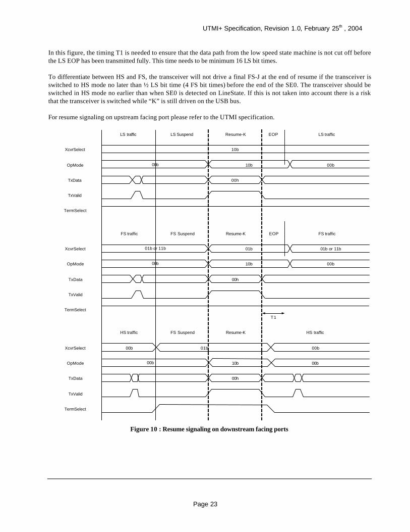
3.2 Suspend / Resume signaling for downstream facing ports This section only applies for downstream facing ports. A port is configured as a downstream facing port when both dppulldown and dmpulldown are active. When a downstream facing port is transmitting a resume (full speed data K), it must be ended with either a low speed EOP (if previously in low / full speed before suspend) or a transition to high speed idle (if previously in high speed). In Figure 10 these different cases are shown.
UTMI+ Specification, Revision 1.0, February 25th , 2004
Page 23
In this figure, the timing T1 is needed to ensure that the data path from the low speed state machine is not cut off before the LS EOP has been transmitted fully. This time needs to be minimum 16 LS bit times. To differentiate between HS and FS, the transceiver will not drive a final FS-J at the end of resume if the transceiver is switched to HS mode no later than ½ LS bit time (4 FS bit times) before the end of the SE0. The transceiver should be switched in HS mode no earlier than when SE0 is detected on LineState. If this is not taken into account there is a risk that the transceiver is switched while “K” is still driven on the USB bus. For resume signaling on upstream facing port please refer to the UTMI specification.
LS traffic LS Suspend Resume-K EOP LS traffic
XcvrSelect
OpMode
TxData
TxValid
10b
00h
HS traffic FS Suspend Resume-K HS traffic
XcvrSelect
OpMode
TxData
TxValid
00b
10b00b 00b
00h
00b
FS traffic FS Suspend Resume-K EOP FS traffic
XcvrSelect
OpMode
TxData
TxValid
10b00b 00b
00h
TermSelect
TermSelect
10b00b 00b
01b01b or 11b 01b or 11b
TermSelect
T1
01b
Figure 10 : Resume signaling on downstream facing ports

UTMI+ Specification, Revision 1.0, February 25th , 2004
Page 24
3.3 Transmit error reporting for downstream facing ports In FS/LS, to indicate that there was a problem with the data transmitter (e.g. buffer underrun) a bit stuff error is generated followed by an EOP. To do this OpMode is switched to 10b to disable the encoding and 00h is loaded into DataIn for at least 1 clock cycle before negating TxValid. However this causes conflict with device resume generation that does not add and EOP when the encoding is not active. Therefore transmit error reporting will only be carried out for at least 1 byte/word. Any greater than this and the generation of the EOP is not guaranteed.
DataIn
OpMode
TxValid
00b 10b 00b
00h
Figure 11 : Transmit error reporting for downstream facing ports

UTMI+ Specification, Revision 1.0, February 25th , 2004
Page 25
3.4 Selection of different signaling modes for upstream and downstream facing ports
For upstream facing ports TermSelect is used as a switch for enabling the pull-up resistor. If XcvrSelect(1) is set to logic ‘0’, TermSelect controls the pull-up resistor on DP. If XcvrSelect is set to “10”, TermSelect is logic ‘1’ and both DpPulldown and DmPulldown are set to logic ‘0’, the pull-up resistor is on DM is switched on. If both DpPulldown and DmPulldown are 1b then TermSelect is used to switch on/off the HS terminations. When DpPulldown and DmPulldown are 1b the pull-up resistor on DP or DM is never switched on. OpMode for downstream facing ports is not only used for disabling bit stuffing but also to distinguish between chirp mode and normal operation mode. Analog Transceiver State XcvrSelect(1:0) TermSelect OpMode(1:0) DpPulldown DmPulldown OTG Host Low Speed 10b 1b 00b 1b 1b Host Low Speed 10b 1b 00b 1b 1b Host Low Speed Suspend 10b 1b 00b 1b 1b Host Low Speed Resume 10b 1b 10b 1b 1b Peripheral Low Speed 10b 1b 00b 0b 0b Peripheral Low Speed Suspend 10b 1b 00b 0b 0b OTG Host Full Speed 01b or 11b 1b 00b 1b 1b Host Full Speed 01b or 11b 1b 00b 1b 1b OTG Peripheral Full Speed 01b 1b 00b 0b 1b Peripheral Full Speed 01b 1b 00b 0b 0b OTG Host High Speed 00b 0b 00b or 11b 1b 1b Host High Speed 00b 0b 00b or 11b 1b 1b Host HS/FS Suspend 01b 1b 00b or 11b 1b 1b Host HS/FS Resume 01b 1b 10b 1b 1b OTG Peripheral High Speed 00b 0b 00b or 11b 0b 1b Peripheral High Speed 00b 0b 00b or 11b 0b 0b Peripheral HS/FSSuspend 01b 1b 00b or 11b 0b 0b Peripheral Resume 01b 1b 10b 0b 0b Host Chirp 00b 0b 10b 1b 1b Peripheral Chirp 00b 1b 10b 0b 0b Tristate Drivers --b -b 01b -b -b
Table 5 : Different signaling modes for upstream and downstream facing ports

UTMI+ Specification, Revision 1.0, February 25th , 2004
Page 26
4. T&MT Connector For UTMI there was a standard connector defined to easily test function cores with transceivers. This definition is extended to suite the UTMI+ extensions. The definition of the different pins is given in Table 6. Pin Function Pin Function Pin Function Pin Function 1 Ddir[3] 26 TxBitstuffEnable 51 GND 76 GND 2 GND 27 GND 52 System Clock 77 ValidH 3 TxBitstuffEnableH 28 VBUS_out 53 GND 78 XcvrSelect1 4 GND 29 VbusValid 54 GND 79 Tx_Enable_N 5 SesEnd 30 VendorID_0 55 FsLsSerialMode 80 GND 6 BValid 31 Data15 56 AValid 81 VDD 7 IdDig 32 GND 57 VDD 82 Data14 8 VDD 33 Data13 58 DischrgVbus 83 Data12 9 GND 34 Data11 59 Tx_SE0 84 GND
10 Tx_DAT 35 GND 60 TxValid 85 Data10 11 ChrgVbus 36 Data9 61 IdPullup 86 Data8 12 DmPulldown 37 Data7 62 GND 87 VDD 13 GND 38 VDD 63 DpPulldown 88 Data6 14 DrvVbus 39 GND 64 IFType0 89 IFType1 15 Vstatus4 40 Force_RxErr 65 GND 90 Clk 16 VDD 41 Data5 66 RxActive 91 Data4 17 Reset 42 Data3 67 OpMode0 92 GND 18 OpMode1 43 GND 68 GND 93 Data2 19 XcvrSelect0 44 Data1 69 VDD 94 Data0 20 TermSelect 45 Vstatus0 70 Vstatus1 95 GND 21 GND 46 GND 71 Vstatus2 96 Vstatus3 22 SuspendM 47 VBUS_in 72 RxValid 97 Rx_DP 23 LineState0 48 Rx_DM 73 GND 98 RX_RCV 24 GND 49 DC_PSNT_N 74 RxError 99 VendorID_1 25 LineState1 50 HostDisconnect 75 TxReady 100 GND/3v3-PSUSHDM[2]
Table 6 : T&MT connector pinning[1]
[1] All non-standard T&MT pinning is marked in italics [2] Pin 100 (GND in T&MT definition) has been designated 3V3-PSU-SHDN. The pin 100 "redefinition" is to do with the implementation of the daughter card. It is a way of choosing whether the daughter card should be supplied through the T&MT connector or from the on board power supplies. If pin 100 is connected to ground then the T&MT supplies the power. If it is left floating then the on board power supplies are used. [3] If DDIR is active then all bidirectional signals become inputs to the transceiver (i.e. for the transceiver to transmit data onto the cable DDIR must be set to logic ‘1’).