uv sources and optics applications, infrastructure and ... · bulk materials for uv optics • high...
TRANSCRIPT

UV Sources and Optics pApplications, Infrastructure and
Component ReliabilityComponent ReliabilityVladimir Liberman, MIT Lincoln Lab
IEEE Reliability UV Workshop
March 14 2012March 14, 2012
UV reliability 1VL 3/14/2012
MIT Lincoln Laboratory

Outline
• Introduction
UV O ti• UV Optics– Sources– Detectors
B lk l t i l– Bulk lens materials– Optical coatings
• Ph t t i ti t l• Photocontamination control– Background information– Contamination mechanisms
Remediation– Remediation
• Conclusions
MIT Lincoln LaboratoryUV reliability 2VL 3/14/2012

Background
• The material for this presentation is mainly derived from – SPIE short course on “UV Optical materials” prepared by– SPIE short course on UV Optical materials prepared by
Vlad Libermanand– SPIE short course on “Contamination Control” prepared by p p y
Rod Kunz• Both above courses were originally designed to address
the technology of 193-nm and 248-nm based photolithographyphotolithography
• However, most of the presented material is relevant for any technology involving UV radiation and optical materials
MIT Lincoln LaboratoryUV reliability 3VL 3/14/2012

Understanding Supplier Infrastructure
• UV optical systems require more stringent material selectionsselections
– More limited than the visible range• An educated user is in a better position to know what is
available for the UV application spacepp p– Better choices can be made when initially acquiring a system
Sources, materials, coatings, detectorsSystem purge, material construction
– Higher reliability performance from a more educated user
MIT Lincoln LaboratoryUV reliability 4VL 3/14/2012
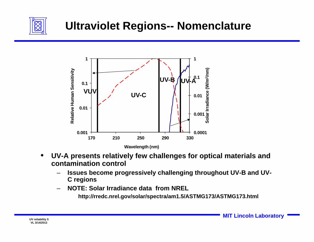
Ultraviolet Regions-- Nomenclature
11
nm)
vity
0.01
0.10.1
adia
nce
(W/m
2 /n
Hum
an S
ensi
tiv
UV-C
UV-B
VUVUV-A
0.0001
0.001
0.001
0.01
170 210 250 290 330
Sola
r Irr
a
Rel
ativ
e
170 210 250 290 330
Wavelength (nm)
• UV-A presents relatively few challenges for optical materials and contamination control
– Issues become progressively challenging throughout UV-B and UV-C regions
– NOTE: Solar Irradiance data from NRELhttp://rredc nrel gov/solar/spectra/am1 5/ASTMG173/ASTMG173 html
MIT Lincoln LaboratoryUV reliability 5VL 3/14/2012
http://rredc.nrel.gov/solar/spectra/am1.5/ASTMG173/ASTMG173.html
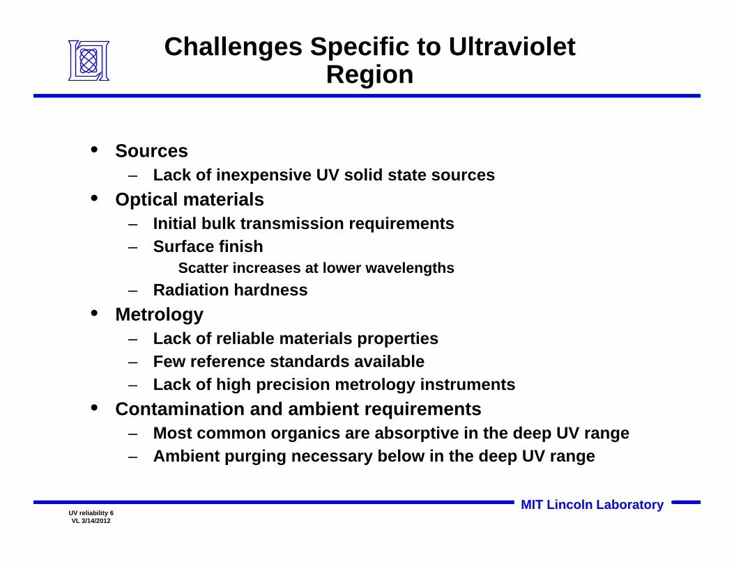
Challenges Specific to Ultraviolet Region
• Sources– Lack of inexpensive UV solid state sources– Lack of inexpensive UV solid state sources
• Optical materials– Initial bulk transmission requirements– Surface finish– Surface finish
Scatter increases at lower wavelengths– Radiation hardness
• MetrologyMetrology– Lack of reliable materials properties– Few reference standards available– Lack of high precision metrology instrumentsg p gy
• Contamination and ambient requirements– Most common organics are absorptive in the deep UV range– Ambient purging necessary below in the deep UV range
MIT Lincoln LaboratoryUV reliability 6VL 3/14/2012
b e t pu g g ecessa y be o t e deep U a ge

Attenuation Lengths of Gaseous H2O, O2 and O3
10000
O2
100
1000
cm-a
tm)
2
1
10
Leng
th, 1
/e(c
Ozone can be a serious problem for
0.1
1
Atte
nuat
ion
O3
UV-C region
0.001
0.01
150 170 190 210 230 250 270 290
O3
H2O
MIT Lincoln LaboratoryUV reliability 7VL 3/14/2012
Wavelength (nm)

UV Light Sources – Overview
• Gaseous discharge sources– Example: Excimer lasers– Example: Excimer lasers– PRO: High power and brightness– CON: Bulky and costly to maintain
• Solid state sourcesSolid state sources– PRO: Compact, easy to use, potentially low cost– However, still in development stages
• Note on units:Note on units:– CW power measured in Watts
Cf. Total solar UV output is 10 W/m2
– Pulsed energy measured in JoulesgyCf. Total solar UV output is 1 J/m2 every 100 ms
MIT Lincoln LaboratoryUV reliability 8VL 3/14/2012

UV Laser Sources Pulsed Gas Discharge
Excimer Laser
Wavel (nm) Pulse Engy (mJ) Spot Size (cm2) Rep Rate (Hz)
308 (XeCl), 222 (KrCl)
>100 mJ Up to several
cm2
100- 1000
351(XeF), 248 (KrF) 193
>100 mJ
Up to several (KrF), 193
(ArF) >100 mJ Up to several
cm2 100- 1000
157 (F2) 10-30 mJ Up to several cm2 Up to 200
Wavel (nm) Pulse Engy (mJ) Spot Size (cm2) Rep Rate (Hz)
Nitrogen Laser
Wavel (nm) Pulse Engy (mJ) Spot Size (cm ) Rep Rate (Hz)
337
>100 mJ
Up to several
cm2
100- 1000
MIT Lincoln LaboratoryUV reliability 9VL 3/14/2012

Excimer Laser
BenefitsHigh pulse energy
Drawbacks– Poor spatial beam profile and pulse-– High pulse energy
– Large beam sizePoor spatial beam profile and pulseto-pulse stability
Solutions exist but expensive– High maintenance
Gas fillsGas fillsChamber optics
Applications– Micromachining
Microlithography– Microlithography248, 193 nm
– Laser eye surgery (193 nm)
MIT Lincoln LaboratoryUV reliability 10
VL 3/14/2012

UV Excimer Laser Applications
• Eye surgery • Micromachining
• Photolithography
MIT Lincoln LaboratoryUV reliability 11
VL 3/14/2012

UV Laser Sources Continuous Wave Gas Discharge
He-Cd
Wavel (nm) Power (W) Beam Diam. (mm)( ) ( ) (mm)
325
10-2
0.5
Wavel (nm) Power (W) Beam Diam. (mm) Method
Ar+ Laser
(mm)
351, 364
Up to 1
1
Fundamental
257 244 U t 1 SHG257, 244 Up to 1 1 SHG
– Laser direct writing– Micromachining
MIT Lincoln LaboratoryUV reliability 12
VL 3/14/2012
– Metrology

UV Laser SourcesSolid State
IR-pumped, nonlinear conversion
Wavel (nm) Pulse Engy (mJ) Spot Size (mm2) Rep Rate (Hz)
355, 266
2 1-2 >1000
213 0.5 1-2 >1000
Tunable Sources: OPO Extensions For example 355 nm pump BBO crystal
Wavel. Range (nm)
Nominal Energy (mJ) Technique
- For example, 355 nm pump, BBO crystal
197-235
1-5 Tripling
203-300 5-30 Sum-frequency
mixing with 355 nm
MIT Lincoln LaboratoryUV reliability 13
VL 3/14/2012

Discharge Lamp Sources for UV application
• Incoherent irradiation– low brightnessg• Uses
– Metrology– Sterilization
MIT Lincoln LaboratoryUV reliability 14
VL 3/14/2012
– Adhesive/sealant curing

UV LEDs
• Extremely attractive– Ultimate portabilityp y– Low cost
• Challenges– Material systems difficult to work y
with– Very low quantum efficiencies– Lifetime issues
• This is a subject of active research– Great interest in the defense and
commercial user communitiesHirayama et al. Electron. Commun. Jpn 93 (2010) 748.
MIT Lincoln LaboratoryUV reliability 15
VL 3/14/2012

UV Light Detection
• Detector choice is determined by source type– Laser or lamp– Laser or lamp– Pulsed or CW
• And application requirements– Response speed– Response speed– Dynamic range– Precision and/or accuracy – DurabilityDurability
MIT Lincoln LaboratoryUV reliability 16
VL 3/14/2012

Common Detector Types and Their Primary Usage
Type Application Salient Features
Pyroelectric Pulse energy or average power for pulsed lasers
Good dynamic range Spectrally flat Long term radiation durability
Low level light detection for Very high gain-photonPhotomultiplier
tube
Low level light detection for metrology applications
Very high gain photon counting possible
Low level laser or lamp sources
High sensitivity Good dynamic range
Photodiodes sourcesArray-based devices, such as dispersive spectrometers and beam profilers
Good dynamic rangeHigh detection speed
Long-term radiation durability Thermopile
Average laser power, pulsed or CW
Long-term radiation durabilityWithstands high power levels Spectrally Flat Standards available
MIT Lincoln LaboratoryUV reliability 17
VL 3/14/2012

Bulk Materials for UV Optics
• High purity fused silica– Well-developed infrastructure– Well-developed infrastructure– Cost and availability depends on purity
• Fluoride crystals– Needed for achromatic correction in optical designs– Needed for achromatic correction in optical designs– More expensive than fused silica
• Some plastics may have limited use
MIT Lincoln LaboratoryUV reliability 18
VL 3/14/2012

Common SiO2 Window Material Transmission (http://www.escoproducts.com)
(all for 10 mm thickness)Pyrex Zerodur
(Aluminosilicate)
UV-grade fused silica
BK-7
Wavelength (nm)Wavelength (nm)
• Great variability in UV cutoff wavelengths for conventional glass windows
• Cost is a major factor when deciding to switch to high purity UV grade fused silica
MIT Lincoln LaboratoryUV reliability 19
VL 3/14/2012
grade fused silica

Transmission of Optical Materials In the VUV Range
100 (all 2 mm thick windows)
80
100
%)
CaF2
LiF
(all 2 mm thick windows)
60
ansm
ittan
ce (%
SapphireLiF
MgF2
20
40Tra
Fused Silica
0120 130 140 150 160 170 180 190 200
Wavelength (nm)
MIT Lincoln LaboratoryUV reliability 20
VL 3/14/2012
Wavelength (nm)

UV Transparent Plastics
• A number of polymers exhibit t i th UV
Poly(methyl methacrylate) Transmission(Plexiglas™ or Lucite™)
Typically, 1/8 inch thickness
transparency in the UV• Polycarbonate• Teflon AF• PMMA• PMMA
• However, most cannot be made intooptical quality windows• Radiation durability is a majorRadiation durability is a major
concern
http://www.plasticgenius.com/2011/05/infrared-and-ultraviolet-transmission.html
MIT Lincoln LaboratoryUV reliability 21
VL 3/14/2012

Common Types of Thin Film Coatings
• Antireflectance coatings– Throughput enhancement– Throughput enhancement– Ghost image reduction
• Full reflectors– Laser windows– Laser windows– Turning mirrors– Retro-reflectors in imaging systems
• Partial reflectorsPartial reflectors– Beam delivery systems– Catadioptric imaging systems
Many custom designsMany custom designs• Filters
– Bandpass/high pass or low pass– Notch filters
MIT Lincoln LaboratoryUV reliability 22
VL 3/14/2012
otc te s– Etc.
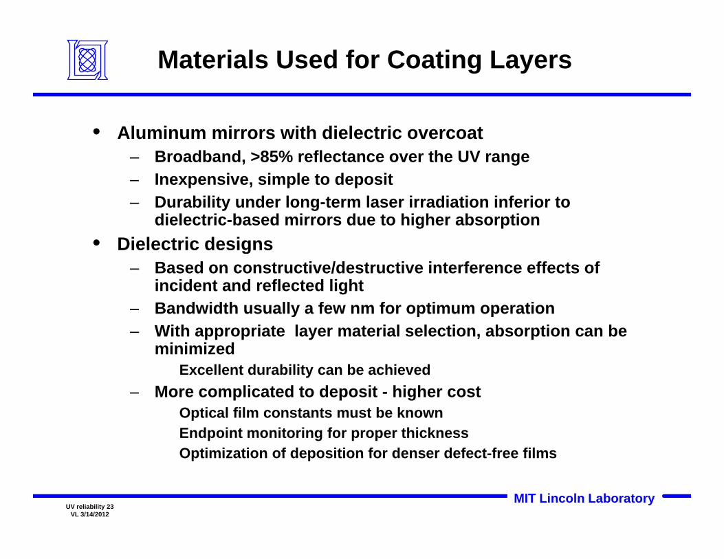
Materials Used for Coating Layers
• Aluminum mirrors with dielectric overcoat– Broadband, >85% reflectance over the UV range
I i i l t d it– Inexpensive, simple to deposit– Durability under long-term laser irradiation inferior to
dielectric-based mirrors due to higher absorption• Dielectric designs• Dielectric designs
– Based on constructive/destructive interference effects of incident and reflected light
– Bandwidth usually a few nm for optimum operationy p p– With appropriate layer material selection, absorption can be
minimizedExcellent durability can be achieved
M li d d i hi h– More complicated to deposit - higher costOptical film constants must be knownEndpoint monitoring for proper thicknessOptimization of deposition for denser defect-free films
MIT Lincoln LaboratoryUV reliability 23
VL 3/14/2012
Optimization of deposition for denser defect free films

Dielectric Coating Layer Materials for Ultraviolet Region
• Basic design involves alternating quarterwave layers of higher and lower index materials than the substratehigher and lower index materials than the substrate
– 3-5 layers for antireflectance designs– Up to 40 layers for high reflector applications– Layer thicknesses in the tens of nanometers, depending on y , p g
wavelength and layer indices• Fluoride or oxide materials may be used
– High indexFluorides: LaF3, GdF3, NdF3Oxides: Al2O3, HfO2, ZrO2
– Low indexFluorides: MgF LiF AlFFluorides: MgF2, LiF, AlF3Oxides: SiO2
MIT Lincoln LaboratoryUV reliability 24
VL 3/14/2012

Examples of Commercial UV Coatings
Broadband Full reflector Narrowband Turning Mirror
B db d AR C ti Laser Line CleanupBroadband AR Coating Laser Line Cleanup
MIT Lincoln LaboratoryUV reliability 25
VL 3/14/2012

“Switching Gears” – From Design to Durability
• What determines longevity of a UV-source-based optical system?system?
• Most common short term failures are not from fundamental material damage but from photoinduced contamination!
• How to separate contamination from material damage?How to separate contamination from material damage?– Contamination is strictly surface-limited, not bulk– Contamination will manifest itself as haze on the surface
As opposed to coating delamination• It is best to consider contamination control during design
stages– As opposed to implementing remediation strategies– Once the onset is observed, it may be too late to save the
optical train from complete replacement!
MIT Lincoln LaboratoryUV reliability 26
VL 3/14/2012

Outline: Photocontamination Control
1. Description and background of photocontamination2 C id i i i l bl2. Considerations prior to optical assembly3. Contamination mechanisms4. Dealing with contaminated optics5. Monitoring for airborne contamination
(material for this section was kindly provided by R. Kunz, ( y p y ,MIT Lincoln Laboratory)
MIT Lincoln LaboratoryUV reliability 27
VL 3/14/2012

1. Overview of Photocontamination
• Precision UV optics are being integrated into a wider range of applications
– Lithography, metrology, interferometry, etc.g p y, gy, y,– Operational requirement very demanding
• Short UV wavelengths interact with ambient in ways not experienced at longer wavelengths, leading to film formation on optical surfaces
– Often referred to a “damage”, “solarization”, or “fogging”• Phenomenon first experienced in space optics
– Full-spectrum solar radiation, large thermal gradients in devices– Significant impact on early space missions– Large investment in infrastructure to manage problem
MIT Lincoln LaboratoryUV reliability 28
VL 3/14/2012

Experience of the Space Optics Community
• Best practices developed to mitigate problem– Defined acceptable levels and established measurement
benchmarksbenchmarks– Contamination requirement as MIL-STD-1246C
• Database of acceptable materials established for use in this applicationapplication
– Standardization of tests for material acceptability• UV Photocontamination specifications, as they pertain to
semiconductor lithographic systems, may be even tightersemiconductor lithographic systems, may be even tighter than those for space optics
MIT Lincoln LaboratoryUV reliability 29
VL 3/14/2012Description and background of photocontamination

Important Processes in Photocontamination
M (gas)
Vapor Source or GenerationRadiation of wavelength
Mass Transport
M (gas)
Gas-surface equilibrium
LENS
M (surf) M (surf) M (surf) M (surf) M (surf)
Photochemical formation of contaminationof contamination
Afterwards: Identification, cleaning, and removal of the contaminant
MIT Lincoln LaboratoryUV reliability 30
VL 3/14/2012
, g,

2. Considerations Prior to Optical Assembly
Its easier to build it right the first time than it is to remediate a poor d idesign...but the designer needs to understand the potential sources of contamination.
• Operating environment • Construction materialsConstruction materials• Stray light – the aggravating factor
MIT Lincoln LaboratoryUV reliability 31
VL 3/14/2012

Time Variability in Ambient Gas Composition
Episodic contamination can be harder to quantify – Need real-time monitors
MIT Lincoln LaboratoryUV reliability 32
VL 3/14/2012
Gronheid et al., In-line monitoring of acid and base contaminants at low ppt-levels for 193nm lithography, Proc. SPIE Vol. 5754, p. 1591 (2005).

Example: Identification of “Contamination-Free” Flexible Purge-Gas Tubing
3.E+05
3.E+05F F
FF
FF
FF
F3C
CF2
CF3
2 E+05
2.E+05
coun
ts)
FFF
F
F3C CF2
F
FF
FF
FF
F FCHF3
Both samples
1.E+05
2.E+05
Sign
al (c
Tubing A
Both sampleswere billed as“fluoropolymers”
0.E+00
5.E+04
3 4 5 6 7 8 9 10
Tubing B
Retention Time (minutes)
For 1-meter of tubing with 0.5-cm ID, nitrogen flowing at 1 liter perminute will be contaminated by:
11 ppb of ario s fl orocarbons for T bing A
MIT Lincoln LaboratoryUV reliability 33
VL 3/14/2012
- 11 ppb of various fluorocarbons for Tubing A- <0.1 ppb total volatile organic compounds for Tubing B

Potential Sources of Contamination
• Potting and/or encapsulation layers• Adhesives• Adhesives• Tapes• Lubricants
S l t• Sealants• Photoresists• Conformal coatings (paint, anodization, etc.)• ..and just about anything else containing organic carbon
MIT Lincoln LaboratoryUV reliability 34
VL 3/14/2012

UV Degradation of SiliconesVIRGIN SURFACE AT 0 25uJ/cm2 pulseCH VIRGIN SURFACE AT 0.25uJ/cm -pulse
SiO
OO
OSi
Si
Si
CH3
H3C
H3C CH3
CH3
CH3
CH3H3C
CH3
CH3
CH3
SiOSiOSiOSiOSi
CH3CH3H3C
H3C
H3C CH3SiOSiCH3
CH3
CH3
CH3
CH3
CH3
OSiO
O
O
Si
SiSi
CH3
H3C
H3CCH3
CH3
CH3
CH3H3C
Si
O
CH3
CH3
CH3
CH3
CH3
SiOH
CH3
H3C
CH3
VIRGIN SURFACE AT 0.27uJ/cm2-pulse
CH3
CH3
CH3
CH3
SiOSiOSiOSi
CH3CH3H3C
H3C
H3C CH3SiOSiOSi
CH3
CH3
CH3 CH3
CH3
CH3
H3C
H3C
SiOSiCH3
CH3
CH3
CH3
CH3
CH3
2.7%55%2%
33%
52%32%12%3%
SiO
CH3
CH3
H3C
CH3n
5.3%
SiO
CH3
CH3
H3C
CH3n
RTVSilicone Paste
OSiOH3C
CH3H3C
Si CH3
CH3Si
O OSiH3C
CH
CH3H3C
43.4%
6.5%
10.4%
38.7%
CH3
CH3
CH3
CH3
SiOSiOSiOSi
CH3CH3H3C
H3C
H3C CH3
OSiO
SiH3C
CH3H3C
Si
O
CH3
CH3
47%
38%
5%
1%
O
O
Si
SiSi
CH3
H3CCH3
CH3
CH3
O
OSiO
OO
Si
Si
Si
CH
H3C
H3C CH3
CH3
CH3H3C
Si
O
CH3
CH3
CH3CH3
SiOSiOSiOSiOSiH3C
H3C CH3
CH3
CH3
OO
Si
Si
CH3
H3C CH3
CH3
CH3
SiO
O
OSiSi
H3C
H3C CH3
CH3H3C
SiOSiOSi
CH3 CH3
CH
H3CSiOSiCH3
CH3
CH3
CH3
O
O
Si
SiSi
CH3
H3CCH3
CH3
CH3
O 5%
4%3%
MIT Lincoln LaboratoryUV reliability 35
VL 3/14/2012
PREIRRADIATED SURFACE AT 13 uJ/cm2-pulse
OSiCH3
H3C
3
O SiCH3H3C
CH3CH3CH3H3C CH3
OO
SiCH3 CH3
CH3SiOSiOSi
CH3
CH3
CH3
CH3
H3CCH3 CH3
PREIRRADIATED SURFACE AT 13 uJ/cm2-pulse

3. Contamination Mechanisms
• Origins of contaminating vapor and mechanisms of outgassingoutgassing
• Mass transport to the lens• Beam-induced chemistry – “photocontamination”• Deposition models and the effect of wavelength• Deposition models and the effect of wavelength• Mechanisms and composition of deposits
MIT Lincoln LaboratoryUV reliability 36
VL 3/14/2012

Mass Transport to the Lens
• Airborne – Viscous gas flow (molecular flow such as that found in space
and particle beam optics not possible)and particle beam optics not possible)– Directed flow can increase or decrease contamination rate –
it depends where the contaminating vapor is originating!• Surface creep
– Implicated in some types of oil-related contamination– Surface tension is the driving force– Distances can be surprisingly long (>cm)
• Surface diffusion– Not well understood, but rates can be high (>m/sec)– Related to surface creep, but active at the molecular rather
than bulk level
MIT Lincoln LaboratoryUV reliability 37
VL 3/14/2012

Outgassing Test Used in Space Industry: ASTM E 595
• Material held at 125 °C for 24 hours– Comparison of initial and final sample weight yields the Total
Mass Loss (TML)Mass Loss (TML)• A cold plate at 25 °C is used to collect outgassing material
– Amount of collected mass is the Collected Volatile Condensable Material (CVCM)
• Sample can then be placed in 50% humidity environment at 25 °C for 24 hours
– Final weight yields Water Vapor Retained (WVR)• Unlike space optics industry, no universal test exists for
litho/UV Systems optics
MIT Lincoln LaboratoryUV reliability 38
VL 3/14/2012

Outgassing Characteristics(An Example from NASA Database)
Material TML% at 75 °C TML% at 125 °C CVCM (%)*
Adhesives
R-2560 1.58 1.53 n/a
RTV-566 0.11 0.26 0.02
DC 93-500 0.07 0.08 0.05
Films
Kapton FEP n/a 0.25 0.01
Kapton H n/a 1.17 0.00
Mylar n/a 0.32 0.04
FEP Teflon n/a 0.77 0.35
Oils and Greases
Brayco 815Z n/a 0.25 0.01
Braycote 803 n/a 0.24 0.13
Krytox 143AD n/a 28.54 5.71
Vakote MLD73-91 0.40 n/a n/a
Paints and Coatings
S13G/LO 0.45 1.00 0.13
Chemglaze Z306 2.40 2.52 0.07
DC Q9-6313 0.40 0.39 n/a
MIT Lincoln LaboratoryUV reliability 39
VL 3/14/2012
Aremco 569 2.28 3.58 n/a
LMSC 1170 1.88 2.89 n/a
*Collected Volatile Condensable Materials

4. Dealing With Contaminated OpticsIdentification, Mitigation, and Remediation
• Confirmation that contamination has occurred– Optical effects– Optical effects– Chemical identification
• Identification of the origin of the contaminating vapor• Elimination of the source of the vapor• Elimination of the source of the vapor
– Removal– Shrouding
• Cleaning the optical surface• Cleaning the optical surface– In situ methods if possible
• Silicone contamination cannot be cleaned optics have to• Silicone contamination cannot be cleaned– optics have to be replaced
MIT Lincoln LaboratoryUV reliability 40
VL 3/14/2012

Optical Effects of Contamination
• Scattering– Leads to increased flare in litho tools
Many published methods to measure, track, and quantifyTracking flare over time the single most useful diagnostic
– Quantified ex situ via the Bidirectional Reflectance Distribution Function (BRDF)
Scattered intensity versus angle (off specular)Scattered intensity versus angle (off specular)– Severe contamination visible to naked eye
Scattering of visible wavelengthsUsually in pattern of lens exposure
• Absorption– Decreased system transmission– Increased or different thermal signatures– Increase in cross-field non-uniformity
• Periodic measurements of both BRDF/flare and transmission provides the earliest indication of
t i ti
MIT Lincoln LaboratoryUV reliability 41
VL 3/14/2012
contamination

5. Airborne ContaminationWhat Needs To Be Detected?
• All compounds that can cause lens contamination– Siloxanes (<ppt)– Phosphonates (<ppb)– Hydrocarbons (>ppb)– Sulfur dioxide (“sulfate”), ammonia, other anions that can cause
lt f ti ( it t hl id )salt formation (nitrates, chloride)
• Time averaged values useful (~hours)
• Best if real time (~minutes)– Quantify concentration transients– Correlate with other activities - troubleshooting
MIT Lincoln LaboratoryUV reliability 42
VL 3/14/2012

Summary
• There are a number of unique applications utilizing ultraviolet irradiation
Semiconductor processing– Semiconductor processing– Medical– Micromachining
• These applications require a proper selection and• These applications require a proper selection and understanding of UV sources and optical materials
– Recent studies, stimulated by excimer laser-based UV lithography for semiconductor processing, helped to advance the understanding of this range
• Photocontamination of optics is a unique problem for the UV range
Hi h h t b d b ki f t i– High photon energy causes bond breaking of most organics– Contamination needs to be well controlled to ensure long
term reliability of optical systems
MIT Lincoln LaboratoryUV reliability 43
VL 3/14/2012