vax7000 pocket guide
TRANSCRIPT

digital equipment corporationmaynard, massachusetts
VAX 7000Pocket Service Guide
Order Number EK–7000A–PG.001
This manual is intended for Digital service engineers. It supplies easy-to-access key information on VAX 7000 systems.

First Printing, September 1992
The information in this document is subject to change without notice and shouldnot be construed as a commitment by Digital Equipment Corporation.
Digital Equipment Corporation assumes no responsibility for any errors that mayappear in this document.
The software, if any, described in this document is furnished under a license andmay be used or copied only in accordance with the terms of such license. No re-sponsibility is assumed for the use or reliability of software or equipment that isnot supplied by Digital Equipment Corporation or its affiliated companies.
Copyright © 1992 by Digital Equipment Corporation.
All Rights Reserved.Printed in U.S.A.
The following are trademarks of Digital Equipment Corporation:
DEC OpenVMS VAXBIDEC LANcontroller PDP VAXclusterDECnet ULTRIX VAXELNDECUS UNIBUS XMIDWMVA VAX
FCC NOTICE: The equipment described in this manual generates, uses, and mayemit radio frequency energy. The equipment has been type tested and found tocomply with the limits for a Class A computing device pursuant to Subpart J ofPart 15 of FCC Rules, which are designed to provide reasonable protection againstsuch radio frequency interference when operated in a commercial environment. Operation of this equipment in a residential area may cause interference, in whichcase the user at his own expense may be required to take measures to correct theinterference.

iii
Contents
Preface ...................................................................................................... xi
Chapter 1 Registers1.1 KA7AA Registers ................................................................... 1-21.2 MS7AA Registers ................................................................. 1-271.3 I/O Port Registers................................................................. 1-351.4 DWLMA Registers ............................................................... 1-40
Chapter 2 Addressing2.1 VAX 7000 Block Diagram ...................................................... 2-22.2 LSB Address Space ................................................................ 2-32.3 XMI Addresses ....................................................................... 2-62.4 VAXBI Addresses ................................................................... 2-7
Chapter 3 Console3.1 Console Commands ................................................................ 3-23.2 Environment Variables .......................................................... 3-93.3 Device Name Fields ............................................................. 3-113.4 Command Syntax ................................................................. 3-123.5 Boot Command ..................................................................... 3-143.6 Cdp Command ...................................................................... 3-173.7 Show Configuration Command ........................................... 3-183.8 Show Device Command ....................................................... 3-193.9 Show Network Command .................................................... 3-203.10 Show Power Command ........................................................ 3-21

iv
Chapter 4 Diagnostics4.1 Test Command ....................................................................... 4-24.2 Set Host Command — Running DUP-Based Diagnostics
and Utilities .......................................................................... 4-104.3 Set Host Command — Running Diagnostics on a Remote
XMI Adapter ........................................................................ 4-12
Chapter 5 FRU Locations5.1 FRUs Common to Every Platform ........................................ 5-25.2 Platform Cables ...................................................................... 5-65.3 FRUs in the XMI Plug-In Unit.............................................. 5-85.4 FRUs in the Disk Plug-In Unit........................................... 5-105.5 FRUs in the Battery Plug-In Unit...................................... 5-12
Chapter 6 Controls and Indicators6.1 Control Panel.......................................................................... 6-26.2 TF85 Removable Media Device ............................................. 6-36.3 Cabinet Control Logic Module ............................................... 6-46.4 IOP Module............................................................................. 6-56.5 KA7AA Processor Module ...................................................... 6-66.6 Power Regulator ..................................................................... 6-86.7 AC Input Box .......................................................................... 6-96.8 BA651 XMI PIU Power Regulators ..................................... 6-106.9 DWLMA Module .................................................................. 6-126.10 BA654 Disk PIU ................................................................... 6-13
Chapter 7 Restoring Corrupted ROMs7.1 Restoring a Corrupted EEPROM .......................................... 7-27.2 Restoring Corrupted Firmware on an Adapter .................... 7-37.3 Restoring Corrupted Firmware on a CPU ............................ 7-7
Chapter 8 System Errors8.1 Machine Check Frame ........................................................... 8-28.2 Machine Check Parse Tree .................................................... 8-58.3 Hard Error Parse Tree ......................................................... 8-12

v
8.4 Soft Error Parse Tree ........................................................... 8-208.5 I/O Port Parse Tree .............................................................. 8-218.6 DWLMA Parse Tree ............................................................. 8-23
Examples2-1 Examining the Device Register of VAXBI Node 7 ............... 2-73-1 Boot Command — Booting from an InfoServer .................. 3-143-2 Cdp Command...................................................................... 3-173-3 Show Configuration Command ........................................... 3-183-4 Show Device Command ....................................................... 3-193-5 Show Network Command .................................................... 3-203-6 Show Power Command ........................................................ 3-214-1 Test Command — System Test ............................................. 4-24-2 Test Command — Write/Read/Compare Test of All Disks
Not Associated with Controller "a" ....................................... 4-44-3 Test Command — Destructive Exercising Selected, Then
Aborted ................................................................................... 4-64-4 Output from Test Command — Quiet Qualifier Set ............ 4-64-5 Test Command — Detection of Memory Data Compare
Error ....................................................................................... 4-74-6 Test Command — Use of Wildcard ....................................... 4-84-7 Test Command — Test All Devices Associated with XMI0 . 4-94-8 Set Host Command — Running DUP-Based Diagnostics
and Utilities .......................................................................... 4-104-9 Set Host Command — Running Diagnostics on a Remote
XMI Adapter, Failing Case .................................................. 4-124-10 Set Host Command — Running Diagnostics on a Remote
XMI Adapter, Passing Case ................................................. 4-137-1 Using the Build EEPROM Command to Restore a
Corrupted EEPROM .............................................................. 7-27-2 Booting LFU ........................................................................... 7-37-3 LFU Display and Show Commands ...................................... 7-57-4 LFU Update Command ......................................................... 7-67-5 LFU Exit Command............................................................... 7-67-6 Preparing the Source System to Restore Corrupted
Firmware on a CPU ............................................................... 7-87-7 Running Kermit and Setting Parameters ............................ 7-87-8 Downline Loading Code to Corrupted FEPROMs................ 7-9
Figures1-1 LDEV — Device Register ....................................................... 1-31-2 LBER — Bus Error Register ................................................. 1-3
vi
1-3 LCNR — Configuration Register .......................................... 1-41-4 LMMR0–7 — Memory Mapping Registers ........................... 1-41-5 LBESR0–3 — Bus Error Syndrome Registers ..................... 1-41-6 LBECR0–1 — Bus Error Command Registers ..................... 1-51-7 LIOINTR — I/O Interrupt Register ...................................... 1-51-8 LIPINTR — Interprocessor Interrupt Register .................... 1-51-9 LMODE — Mode Register ..................................................... 1-61-10 LMERR — Module Error Register ...................................... 1-71-11 LLOCK — Lock Address Register ......................................... 1-71-12 LDIAG — Diagnostic Control Register ................................. 1-81-13 LTAGA — Tag Address Register .......................................... 1-81-14 LTAGW — Tag Write Data Register .................................... 1-81-15 LCON — Console Communication Registers ....................... 1-91-16 LPERF — Performance Counter Control Register .............. 1-91-17 LCNTR — Performance Counter Registers .......................... 1-91-18 LMISSADDR — Last Miss Address Register ..................... 1-101-19 ICCS — Interval Clock Control and Status Register ......... 1-141-20 NICR — Next Interval Count Register ............................... 1-141-21 ICR — Interval Count Register ........................................... 1-151-22 TODR — Time-of-Day Register........................................... 1-151-23 MCESR — Machine Check Error Summary Register ....... 1-151-24 SID — System Identification Register ................................ 1-151-25 PCSCR — Patchable Control Store Control Register ........ 1-161-26 ECR — Ebox Control Register ............................................ 1-161-27 BIU_CTL — BIU Control Register ..................................... 1-171-28 DIAG_CTL — Diagnostic Control Register ........................ 1-171-29 BIU_STAT — BIU Status Register ..................................... 1-181-30 BIU_ADDR — BIU Address Register ................................. 1-181-31 FILL_SYND — Fill Syndrome Register ............................. 1-181-32 FILL_ADDR — Fill Address Register ................................. 1-191-33 CHALT — Console Halt Register ........................................ 1-191-34 VMAR — VIC Memory Address Register ........................... 1-191-35 VTAG — VIC Tag Register .................................................. 1-191-36 VDATA — VIC Data Register ............................................. 1-201-37 ICSR — Ibox Control and Status Register ......................... 1-201-38 BPCR — Ibox Branch Prediction Control Register ............ 1-201-39 MP0BR — Mbox P0 Base Register ..................................... 1-211-40 MP0LR — Mbox P0 Length Register .................................. 1-211-41 MP1BR — Mbox P1 Base Register ..................................... 1-211-42 MP1LR — Mbox P1 Length Register .................................. 1-211-43 MSBR — Mbox System Base Register ................................ 1-221-44 MSLR — Mbox System Length Register ............................ 1-221-45 MMAPEN — Mbox Memory Management Enable
Register ................................................................................. 1-22

vii
1-46 PAMODE — Physical Address Mode Register ................... 1-221-47 MMEADR — Memory Management Exception Address
Register ................................................................................. 1-231-48 MMEPTE — Memory Management Exception PTE
Address Register .................................................................. 1-231-49 MMESTS — Memory Management Exception Status
Register ................................................................................. 1-231-50 TBADR — Translation Buffer Parity Address Register .... 1-241-51 TBSTS — Translation Buffer Parity Status Register ........ 1-241-52 PCADR — P-Cache Parity Address Register ..................... 1-241-53 PCSTS — P-Cache Status Register .................................... 1-251-54 PCCTL — P-Cache Control Register .................................. 1-251-55 LDEV — Device Register ..................................................... 1-281-56 LBER — Bus Error Register ............................................... 1-281-57 LCNR — Configuration Register ........................................ 1-291-58 IBR — Information Base Repair Register .......................... 1-291-59 LBESR0–3 — Bus Error Syndrome Registers ................... 1-291-60 LBECR0–1 — Bus Error Command Registers ................... 1-301-61 MCR — Memory Configuration Register ............................ 1-301-62 AMR — Address Mapping Register .................................... 1-301-63 MSTR0–1 — Memory Self-Test Registers .......................... 1-311-64 FADR — Failing Address Register ..................................... 1-311-65 MERA — Memory Error Register A ................................... 1-311-66 MSYNDA — Memory Syndrome Register A ...................... 1-321-67 MDRA — Memory Diagnostic Register A ........................... 1-321-68 MCBSA — Memory Check Bit Substitute Register A ....... 1-321-69 MERB — Memory Error Register B ................................... 1-331-70 MSYNDB — Memory Syndrome Register B ...................... 1-331-71 MDRB — Memory Diagnostic Register B ........................... 1-331-72 MCBSB — Memory Check Bit Substitute Register B ....... 1-341-73 IBR — Information Base Repair Register .......................... 1-361-74 LILID0–3 — Interrupt Level 0–3 IDENT Registers .......... 1-361-75 LCPUMASK — CPU Interrupt Mask Register .................. 1-371-76 LMBPR — Mailbox Pointer Register .................................. 1-371-77 IPCNSE — I/O Port Chip Node-Specific Error Register.... 1-371-78 IPCVR — I/O Port Chip Vector Register ............................ 1-371-79 IPCMSR — I/O Port Chip Mode Selection Register ........... 1-381-80 IPCHST — I/O Port Chip Hose Status Register ................ 1-381-81 IPCDR — I/O Port Chip Diagnostic Register ..................... 1-391-82 LDIAG — Diagnostic Register ............................................ 1-401-83 IMSK — Interrupt Mask Register ...................................... 1-411-84 LEVR — Error Vector Register ........................................... 1-411-85 LERR — Error Register ....................................................... 1-411-86 LGPR — General Purpose Register .................................... 1-42
viii
1-87 IPR1 — Interrupt Pending Register 1 ................................ 1-421-88 IPR2 — Interrupt Pending Register 2 ................................ 1-421-89 IIPR — Interrupt in Progress Register ............................... 1-421-90 XDEV — Device Register .................................................... 1-431-91 XBER — Bus Error Register ............................................... 1-441-92 XFADR — Failing Address Register ................................... 1-451-93 XFAER — Failing Address Extension Register ................. 1-451-94 IBR — Information Base Repair Register .......................... 1-452-1 VAX 7000 Block Diagram ...................................................... 2-22-2 Virtual Address Space Layout ............................................... 2-32-3 Physical Address Space Layouts ........................................... 2-35-1 Platform Cabinet (Front) Showing FRU Locations .............. 5-25-2 Platform Cabinet (Rear) Showing FRU Locations ............... 5-45-3 Platform Cabinet (Rear and Front) Showing Cables ........... 5-65-4 XMI Plug-In Unit (Front) Showing FRU Locations............. 5-85-5 Disk Plug-In Unit (Front) Showing FRU Locations........... 5-105-6 Battery Plug-In Unit (Rear) Showing FRU Locations....... 5-126-1 Control Panel ......................................................................... 6-26-2 TF85 Controls and Indicators ............................................... 6-36-3 CCL Module LEDs ................................................................. 6-46-4 IOP (E2044-AA) Module LED............................................... 6-56-5 Processor (E2045) LEDs After Self-Test............................... 6-66-6 Power Regulator LEDs .......................................................... 6-86-7 AC Input Box — Indicators on Circuit Breaker ................... 6-96-8 XMI PIU Power Regulators ................................................. 6-106-9 DWLMA (T2028-AA) Module LEDs.................................... 6-126-10 Disk Brick Control Panel ..................................................... 6-138-1 Machine Check Frame ........................................................... 8-28-2 Machine Check Parse Tree .................................................... 8-58-3 Hard Error Parse Tree ......................................................... 8-128-4 Soft Error Parse Tree ........................................................... 8-208-5 IOP Parse Tree ..................................................................... 8-218-6 DWLMA Parse Tree ............................................................. 8-23
Tables1 VAX 7000 Documentation ...................................................... xii2 Related Documents ................................................................ xiv1-1 LSB Required Registers......................................................... 1-21-2 KA7AA-Specific Registers..................................................... 1-61-3 KA7AA Internal Processor Registers .................................. 1-111-4 Gbus Registers ..................................................................... 1-261-5 MS7AA Registers ................................................................. 1-27

ix
1-6 I/O Port Registers................................................................. 1-351-7 LSB Registers ....................................................................... 1-401-8 XMI Registers ....................................................................... 1-432-1 Address Mapping from 30-Bit Mode to 32-Bit Mode............ 2-42-2 LSB Node Base Addresses ..................................................... 2-42-3 Device Type Codes ................................................................. 2-52-4 XMI Node Addresses .............................................................. 2-62-5 Base Addresses of VAXBI Nodes........................................... 2-82-6 Address Offsets of VAXBI Registers ..................................... 2-93-1 Console Commands ................................................................ 3-23-2 Boot Command Options ......................................................... 3-33-3 Cdp Command Options .......................................................... 3-43-4 Clear EEPROM Command Options ...................................... 3-43-5 Create Command Option ....................................................... 3-53-6 Deposit and Examine Command Options ............................. 3-53-7 Set EEPROM Command Options .......................................... 3-63-8 Set Host Command Options .................................................. 3-63-9 Show EEPROM Command Options ...................................... 3-63-10 Show Power Command Options ............................................ 3-73-11 Test Command Options ......................................................... 3-73-12 Update Command Options .................................................... 3-83-13 Environment Variables .......................................................... 3-93-14 Device Name Fields ............................................................. 3-113-15 Console Special Characters ................................................. 3-133-16 Sample Boot Commands ...................................................... 3-163-17 Abbreviations Used in Show Power Command Output ..... 3-226-1 Control Panel Indicator Lights.............................................. 6-26-2 TF85 Lights ............................................................................ 6-36-3 CCL Module LEDs ................................................................. 6-46-4 IOP (E2044-AA) Module LED............................................... 6-56-5 Processor (E2045) LEDs After Self-Test............................... 6-66-6 Self-Test LEDs Indicating Defective DC-to-DC Converter.. 6-76-7 Power Regulator Lights ......................................................... 6-86-8 AC Input Box — Indicators on Circuit Breaker ................... 6-96-9 XMI PIU Power Regulator Lights (Regulators A and B) ... 6-116-10 XMI PIU Power Switches (Regulator B) ............................. 6-116-11 DWLMA (T2028-AA) Module LEDs.................................... 6-126-12 Disk Brick Controls and Indicators .................................... 6-138-1 Machine Check Frame Parameters ...................................... 8-38-2 Machine Check Codes in the Stack Frame ........................... 8-4

xi
Preface
Intended AudienceThis manual is written for the Digital service engineer.
Document StructureThis manual has eight chapters:• Chapter 1, Registers, lists the registers in this system and provides
an illustration of each.• Chapter 2, Addressing, provides information on address space lay-
out, addresses, and device types.• Chapter 3, Console, contains a list of the console commands, syntax,
and error messages.• Chapter 4, Diagnostics, shows examples of running diagnostics on
adapters and device controllers.• Chapter 5, FRU Locations, identifies the field-replaceable units in
the platform.• Chapter 6, Controls and Indicators, discusses the controls and in-
dicators on various components of the system.• Chapter 7, Restoring Corrupted ROMs, provides instructions for
restoring corrupted EEPROMs and for updating corrupted firmware.• Chapter 8, System Errors, includes the machine check frame and
the system parse trees.

xii
Conventions Used in This DocumentThe text shown in command syntax uses these conventions:• Bold text indicates elements to be typed at the terminal.• Brackets ([]) indicate that an element is optional.• Braces ({}) indicate a choice from the enclosed list.• Angle brackets (<>) indicate that the enclosed text is not a literal de-
piction of the element but instead a reference to the kind of item thatcan appear in that position.
The icons shown below are used in illustrations for designating part place-ment in the system described. A shaded area in the icon shows the loca-tion of the component or part being discussed.
Document TitlesTable 1 lists the books in the VAX 7000 documentation set. Table 2 listsother documents that you may find useful.
Table 1 VAX 7000 Documentation
RearFront
Title Order Number
Installation Kit EK–7000A–DK
Site Preparation Guide EK–7000A–SP
Installation Guide EK–700EA–IN
Hardware User Information Kit EK–7001A–DK
Operations Manual EK–7000A–OP
Basic Troubleshooting EK–7000A–TS

xiii
Table 1 VAX 7000 Documentation (Continued)
Title Order Number
Service Information Kit EK–7002A–DK
Pocket Service Guide EK–7000A–PG
Advanced Troubleshooting EK–7001A–TS
Platform Service Manual EK–7000A–SV
System Service Manual EK–7002A–SV
Reference ManualsConsole Reference Manual EK–70C0A–TM
KA7AA CPU Technical Manual EK–KA7AA–TM
MS7AA Technical Manual EK–MS7AA–TM
I/O System Technical Manual EK–70I0A–TM
Platform Technical Manual EK–7000A–TM
Upgrade ManualsKA7AA CPU Installation Guide EK–KA7AA–IN
MS7AA Memory Installation Guide EK–MS7AA–IN
DWLMA XMI PIU Installation Guide EK–DWLMA–IN
H7237 Battery PIU Installation Guide EK–H7237–IN
BA654 Disk PIU Installation Guide EK–BA654–IN
DWMBB VAXBI PIU Installation Guide EK–DWMBB–IN
Removable Media Installation Guide EK–TFRRD–IN

xiv
Table 2 Related Documents
Title Order Number
General Site PreparationSite Environmental Preparation Guide EK–CSEPG–MA
System I/O OptionsCIXCD Interface User Guide EK–CIXCD–UG
DEC FDDIcontroller 400 Installation/ProblemSolving
EK–DEMFA–IP
DEC LANcontroller 400 Installation Guide EK–DEMNA–IN
DEC LANcontroller 400 Technical Manual EK–DEMNA–TM
DSSI VAXcluster Installation and Troubleshoot-ing Manual
EK–410AA–MG
InfoServer 150 Installation and Owner’s Guide EK–INFSV–OM
KFMSA Module Installation and User Manual EK–KFMSA–IM
KFMSA Module Service Guide EK–KFMSA–SV
RF Series Integrated Storage Element User Guide EK–RF72D–UG
TF85 Cartridge Tape Subsystem Owner’s Manual EK–OTF85–OM
Operating System ManualsVMS Upgrade and Installation Supplement: VAX 7000–600 and VAX 10000–600 Series
AA–PRAHA–TE
VMS Network Control Program Manual AA–LA50A–TE
VAXclusters and NetworkingHSC Installation Manual EK–HSCMN–IN
SC008 Star Coupler User’s Guide EK–SC008–UG
VAX Volume Shadowing Manual AA–PBTVA–TE
Peripherals
Installing and Using the VT420 Video Terminal EK–VT420–UG
LA75 Companion Printer Installation and UserGuide
EK–LA75X–UG

Registers 1-1
Chapter 1
RegistersThis chapter is a compilation of the major registers in components of theVAX 7000 system. Each section consists of a list of the registers in thecomponent including register name, mnemonic, and address and illustra-tions of the major registers. Sections include:• KA7AA Registers
— LSB Required Registers— CPU-Specific Registers— Internal Processor Registers— Gbus Registers
• MS7AA Registers• I/O Port Registers• DWLMA Registers
— LSB Registers— XMI Registers

1-2 Registers
1.1 KA7AA Registers
Table 1-1 LSB Required Registers
Mnemonic Register Name Byte Offset
LDEV Device BB 1 + 0000
LBER Bus Error BB + 0040
LCNR Configuration BB + 0080
LMMR0 Memory Mapping 0 BB + 0200
LMMR1 Memory Mapping 1 BB + 0240
LMMR2 Memory Mapping 2 BB + 0280
LMMR3 Memory Mapping 3 BB + 02C0
LMMR4 Memory Mapping 4 BB + 0300
LMMR5 Memory Mapping 5 BB + 0340
LMMR6 Memory Mapping 6 BB + 0380
LMMR7 Memory Mapping 7 BB + 03C0
LBESR0 Bus Error Syndrome 0 BB + 0600
LBESR1 Bus Error Syndrome 1 BB + 0640
LBESR2 Bus Error Syndrome 2 BB + 0680
LBESR3 Bus Error Syndrome 3 BB + 06C0
LBECR0 Bus Error Command 0 BB + 0700
LBECR1 Bus Error Command 1 BB + 0740
LIOINTR I/O Interrupt BSB2 + 0000
LIPINTR Interprocessor Interrupt BSB + 0040
1 BB is the node space base address of the CPU module in hex.2 BSB is the broadcast space base address in hex.

Registers 1-3
Figure 1-1 LDEV — Device Register
Figure 1-2 LBER — Bus Error Register
31 0
DREV
BXB-0100-92
30 1516
DTYPE
31 18 17 16 15 14 13 12 11 10 9 4 3 08 7 6 5 12
RSVD
NSES CTCE DTCE
CDPE CPE2 CPE CE2
CNFE STE TDE
CDPE2
DIE SHE CAE
NXAE
19
BXB-0101-92
<3> <2> <1> <0>
<7> <6> <5> <4>
<11> <10> <9> <8>
<15> <14> <13> <12>
<18> <17> <16>
CE UCE2 UCE
E

1-4 Registers
Figure 1-3 LCNR — Configuration Register
Figure 1-4 LMMR0–7 — Memory Mapping Registers
Figure 1-5 LBESR0–3 — Bus Error Syndrome Registers
31 30 29 28 27 0
RSTSTATNHALTNRSTSTF
BXB-0102-92
CEEN
MBZ
1
31 17 16 11 10 9 4 3 0
BXB-0104-92
8 5
RSVDMODULE_ADDR
2 1
NBANKS AW
IA INT EN
31 0
SYND_0
7 6
RSVD
SYND_1RSVD
SYND_2RSVD
SYND_3RSVD
BXB-0105-92

Registers 1-5
Figure 1-6 LBECR0–1 — Bus Error Command Registers
Figure 1-7 LIOINTR — I/O Interrupt Register
Figure 1-8 LIPINTR — Interprocessor Interrupt Register
31 20 19 18 17 16 15 14 11 10 0
CA <31:0>
7 6
RSVD CID
BXB-0106-92
RSVD P CMD CA
CNF
DIRTYSHARED
DCYCLE
5 3 2
31 16 15 12 11 4 3 0
CPU 0
8 7
MBZ CPU 1CPU 2CPU 3
BXB-0109-92
31 16 15 0
MBZ MASK
BXB-0120-92

1-6 Registers
Table 1-2 KA7AA-Specific Registers
Figure 1-9 LMODE — Mode Register
Mnemonic Register Name Byte Offset
LMODE Mode BB + C00
LMERR Module Error BB + C40
LLOCK Lock Address BB + C80
LDIAG Diagnostic Control BB + D00
LTAGA Tag Address BB + D40
LTAGW Tag Write Data BB + D80
LCON Console Communication BB + E00BB + E40
LPERF Performance Counter Control BB + F00
LCNTR Performance Counter BB + F40BB + F80
LMISSADDR Last Miss Address BB + FC0
31 17 16 15 11 10 9 4 3 08 7 6 5 12
MBZ MBZ
BXB-0130-92
LEVI_REVCLR_LOCK
STCOND_TO
LOCK_MODE PMODE WMODE
BSIZE
Registers 1-7
Figure 1-10 LMERR — Module Error Register
Figure 1-11 LLOCK — Lock Address Register
31 11 10 9 4 3 08 7 6 5
RSVD
BXB-0122-92
ARBDROP ARBCOL
BDATADBEBDATASBE
BMAPPE BSTATPE
BTAGPE PMAPPE
31 30 29 28 0
LADR
BXB-0126-92
MBZ LOCK
MBZ
1

1-8 Registers
Figure 1-12 LDIAG — Diagnostic Control Register
Figure 1-13 LTAGA — Tag Address Register
Figure 1-14 LTAGW — Tag Write Data Register
31 11 10 4 3 07 6 5 12
MBZ
BXB-0121-92
TAG_SEL FRIGN FBDP FBCP
FDBE FSBE
FSHARE FDIRTY SPARE
8
31 19 18 0
TAG_ADDR
BXB-0123-92
MBZ
31 30 29 28 27 0
TAG_DATA
BXB-0124-92
PMAPP VALID SHARED DIRTY
26 25 24 23
BTAGP BSTATP BMAPP
MBZ ��

Registers 1-9
Figure 1-15 LCON — Console Communication Registers
Figure 1-16 LPERF — Performance Counter Control Register
Figure 1-17 LCNTR — Performance Counter Registers
31 0
CON_COM_DATA0
BXB-0129-92
CON_COM_DATA1
0
1
31 24 23 22 21 20 16 15 14 13 12 4 3 08 7 12
N_MASK LC1_SEL LC0_SEL MBZ
BXB-0229-92
LC1_HLT LC1_RUN
MBZ
MA_FREQ LC1_OVFL LC0_OVFL
LC0_HLT LC0_RUN
MBZ
31 0
EV_COUNT0
BXB-0228-92
EV_COUNT1

1-10 Registers
Figure 1-18 LMISSADDR — Last Miss Address Register
31 29 28 0
MBZ MISS_ADDR
BXB-0227-92

Registers 1-11
Table 1-3 KA7AA Internal Processor Registers
Mnemonic Register Name AddressDec Hex Type
KSP Kernel Stack Pointer 0 0 R/W
ESP Executive Stack Pointer 1 1 R/W
SSP Supervisor Stack Pointer 2 2 R/W
USP User Stack Pointer 3 3 R/W
ISP Interrupt Stack Pointer 4 4 R/W
P0BR P0 Base 8 8 R/W
P0LR P0 Length 9 9 R/W
P1BR P1 Base 10 A R/W
P1LR P1 Length 11 B R/W
SBR System Base 12 C R/W
SLR System Length 13 D R/W
CPUID CPU Identification 1 14 E R/W
PCBB Process Control Block Base 16 10 R/W
SCBB System Control Block Base 17 11 R/W
IPL Interrupt Priority Level 1 18 12 R/W
ASTLVL AST Level 1 19 13 R/W
SIRR Software Interrupt Request 20 14 WO
SISR Software Interrupt Summary 1 21 15 R/W
ICCS Interval Clock Control/Status 1 24 18 R/W
NICR Next Interval Count 25 19 WO
ICR Interval Count 26 1A RO
TODR Time-of-Day 27 1B R/W
MCESR Machine Check Error Summary 38 26 WO
SAVPC Console Saved PC 42 2A RO
SAVPSL Console Saved PSL 43 2B RO
1 Initialized on reset.

1-12 Registers
Table 1-3 KA7AA Internal Processor Registers (Continued)
Mnemonic Register Name AddressDec Hex Type
MAPEN Memory Management Enable 1 56 38 R/W
TBIA Translation Buffer InvalidateAll
57 39 WO
TBIS Translation Buffer InvalidateSingle
58 3A WO
PME Performance Monitor Enable 1 61 3D R/W
SID System Identification 62 3E RO
TBCHK Translation Buffer Check 63 3F WO
LMBOX Mailbox 121 79 WO
INTSYS Interrupt System Status 2 122 7A R/W
PMFCNT Performance Monitoring Facil-ity Count
123 7B R/W
PCSCR Patchable Control Store Con-trol2
124 7C R/W
ECR Ebox Control 125 7D R/W
MTBTAG Mbox TB Tag Fill 2 126 7E WO
MTBPTE Mbox TB PTE Fill 2 127 7F WO
BIU_CTL BIU Control 160 A0 WO
DIAG_CTL Diagnostic Control 161 A1 WO
BC_TAG B-Cache Error Tag 162 A2 RO
BIU_STAT BIU Status 164 A4 W1C
BIU_ADDR BIU Address 166 A6 RO
FILL_SYN Fill Syndrome 168 A8 RO
FILL_ADDR Fill Address 170 AA RO
IPR_STR_COND
STxC Pass Fail/CEFSTS 172 AC R/W
1 Initialized on reset.2 Testability and diagnostic use only; not for software use in normal operation.

Registers 1-13
Table 1-3 KA7AA Internal Processor Registers (Continued)
Mnemonic Register Name AddressDec Hex Type
BCDECC Software ECC 174 AE WO
CHALT Console Halt 176 B0 R/W
SIO Serial I/O 178 B2 R/W
SOE_IE SROM_OE_Serial I.E. 180 B4 R/W
QW_PACK Pack I/O to QW 184 B8 WO
CLR_IO_PACK
Clear QW I/O Pack 185 B9 WO
VMAR VIC Memory Address 208 D0 R/W
VTAG VIC Tag 209 D1 R/W
VDATA VIC Data 210 D2 R/W
ICSR Ibox Control and Status 211 D3 R/W
BPCR Ibox Branch Prediction Control2 212 D4 R/W
BPC Ibox Backup PC 214 D6 RO
BPCUNW Ibox Backup PC with RLOGUnwind 3
215 D7 RO
MP0BR Mbox P0 Base 2 224 E0 R/W
MP0LR Mbox P0 Length 2 225 E1 R/W
MP1BR Mbox P1 Base 2 226 E2 R/W
MP1LR Mbox P1 Length 2 227 E3 R/W
MSBR Mbox System Base 2 228 E4 R/W
MSLR Mbox System Length 2 229 E5 R/W
MMAPEN Mbox Memory Management Enable 2
230 E6 R/W
PAMODE Physical Address Mode 231 E7 R/W
MMEADR Memory Management Excep-tion Address
232 E8 RO
2 Testability and diagnostic use only; not for software use in normal operation.3 Chip use only; not for software use.

1-14 Registers
Table 1-3 KA7AA Internal Processor Registers (Continued)
Figure 1-19 ICCS — Interval Clock Control and Status Register
Figure 1-20 NICR — Next Interval Count Register
Mnemonic Register Name AddressDec Hex Type
MMEPTE Memory Management Excep-tion PTE Address
233 E9 RO
MMESTS Memory Management Excep-tion Status
234 EA RO
TBADR Translation Buffer Parity Ad-dress
236 EC RO
TBSTS Translation Buffer ParityStatus
237 ED R/W
PCADR P-Cache Parity Address 242 F2 RO
PCSTS P-Cache Status 244 F4 R/W
PCCTL P-Cache Control 248 F8 R/W
31 30 4 3 08 7 6 5
MBZ
BXB-0167-92
1
ERR INTR IE
SGL XFR RUN
MBZ
31 0
NINT_COUNT
BXB-0169-92

Registers 1-15
Figure 1-21 ICR — Interval Count Register
Figure 1-22 TODR — Time-of-Day Register
Figure 1-23 MCESR — Machine Check Error Summary Register
Figure 1-24 SID — System Identification Register
31 0
INT_COUNT
BXB-0168-92
31 0
TOD
BXB-0166-92
31 0
BXB-0236-92
MCESR
31 24 23 16 15 08 7
CPU_TYPE 0 0 0 0 0 0 0 0 MIC_OPTIONS MIC_REV
BXB-0180-92

1-16 Registers
Figure 1-25 PCSCR — Patchable Control Store Control Register
Figure 1-26 ECR — Ebox Control Register
31 13 12 11 10 9 08 7
0 0 0 0 0 0 0 0 0 0 0 0 0 0 0 0 0 0 0 0 0 0 0 0 0 0 0
BXB-0137-92
PCS_DATA SHIFT
PCS_WRITE PCS_ENB
PAR_PORT_DIS
31 30 23 22 21 19 18 17 16 15 14 13 12 4 3 07 6 5 12
0 0 0 0 0 0 0 0 0 0 0 0 0 0 0
BXB-0138-92
FBOX_ST4_BYPASS_ENB TO_EXT
FBOX_ENB
TO_CLOCK TO_TEST
TO_OCCURRED
PMF_CLEAR PMF_LFSR
PMF_EMUX PMF_PMUX
PMF_ENB FBOX_TEST_ENB
00

Registers 1-17
Figure 1-27 BIU_CTL — BIU Control Register
Figure 1-28 DIAG_CTL — Diagnostic Control Register
31 30 28 27 24 23 20 19 16 15 14 13 12 11 10 9 4 3 08 7 6 5 12
X X X X 0 0 0 0 X X X X X
BXB-0213-92
BC_SIZE WS_IO
IO_MAP "PV"
QW_IO_RD PCACHE_MODE
X X X 0
BC_SPD BC_FHIT
OE ECC
BC_ENBNOTE: X bits read inverted values from DIAG_CTL
31 28 27 26 24 23 21 20 16 15 14 13 12 11 10 08 7 6 5
X X X X 0 0 0 0 0 X X X X X X X X X X X
BXB-0212-92
SW_ECC TODR_TEST TODR_INC PACK_DISABLE MAB_EN
PM_ACCS_TYPE PM_HIT_TYPE DIS_ECC_ERR

1-18 Registers
Figure 1-29 BIU_STAT — BIU Status Register
Figure 1-30 BIU_ADDR — BIU Address Register
Figure 1-31 FILL_SYND — Fill Syndrome Register
BXB-0162-92
FILL_SEO FILL_QW FILL_IRD
FILL_DPERRFILL_CRD FILL_ECC BIU_SEO
BIU_DSP_CMDBC_TCPERR
BC_TPERR BIU_SERR BIU_HERR
0
BIU_ADDR FILL_ADDR
LOST_WRITE FILL_DSP_CMD
31 30 29 28 27 21 20 19 16 15 14 13 12 11 10 9 4 3 08 7 6 12
0 0 0 0 0 0 0
BIU_ADDR
BXB-0186-92
31 4 05
X X X X X
63 7 6 014 13
HI LO
BXB-0163-92
0

Registers 1-19
Figure 1-32 FILL_ADDR — Fill Address Register
Figure 1-33 CHALT — Console Halt Register
Figure 1-34 VMAR — VIC Memory Address Register
Figure 1-35 VTAG — VIC Tag Register
FILL_ADDR
BXB-0187-92
31 4 05
X X X X X
31 0
CON_BASE_ADDR
BXB-0170-92
31 11 10 4 3 0 5 1 2
ADDR 0 0
BXB-0132-92
ROW_INDEX SUB_BLOCK
LW
31 11 10 9 4 3 0 8 7
TAG 0 0
BXB-0133-92
TAG_P DATA_P DATA_V
1-20 Registers
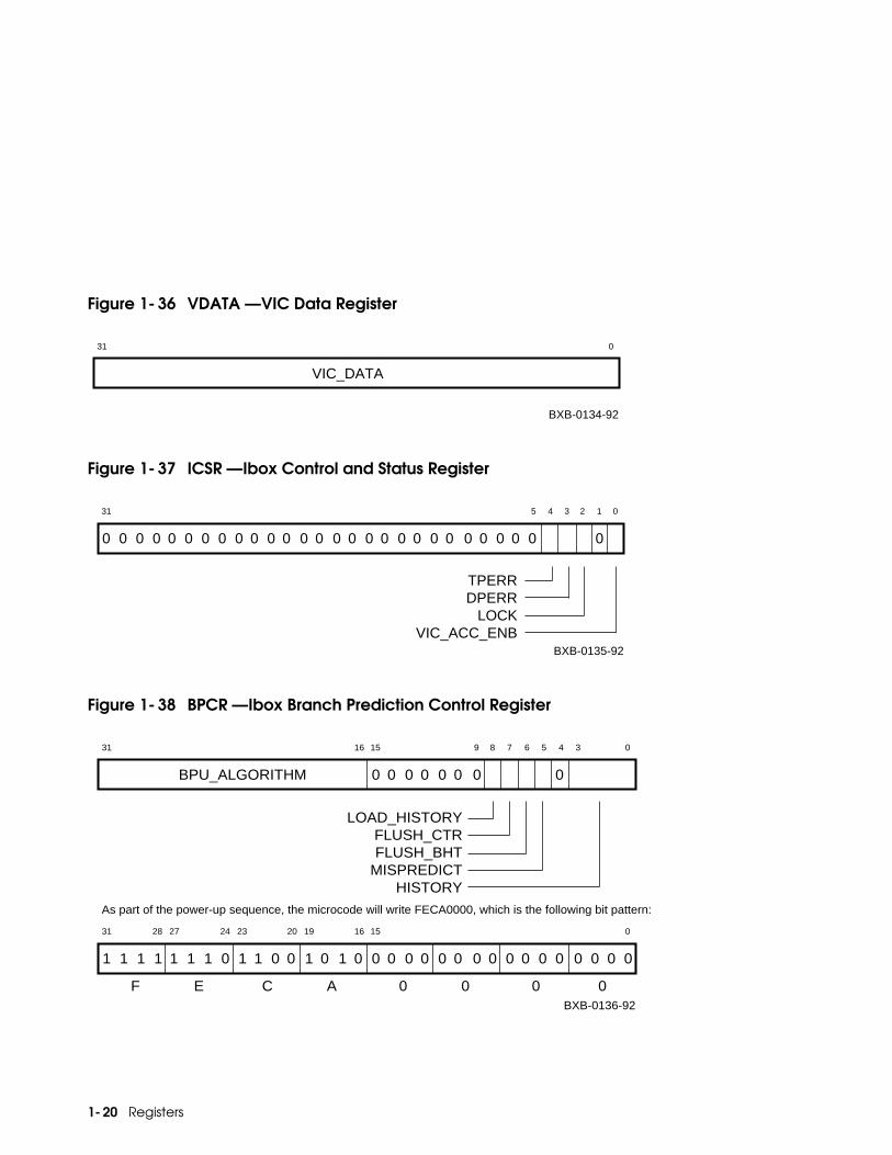
Figure 1-36 VDATA — VIC Data Register
Figure 1-37 ICSR — Ibox Control and Status Register
Figure 1-38 BPCR — Ibox Branch Prediction Control Register
31 0
VIC_DATA
BXB-0134-92
31 4 3 05
0
12
0 0 0 0 0 0 0 0 0 0 0 0 0 0 0 0 0 0 0 0 0 0 0 0 0 0 0
BXB-0135-92
TPERR DPERR
LOCK VIC_ACC_ENB
31 16 15 9 4 3 08 7 6 5
BPU_ALGORITHM 0 0 0 0 0 0 0 0
31 28 27 24 23 20 19 16 15 0
1 1 1 1 1 1 1 0 1 1 0 0 1 0 1 0 0 0 0 0 0 0 0 0 0 0 0 0 0 0 0 0
BXB-0136-92
As part of the power-up sequence, the microcode will write FECA0000, which is the following bit pattern:
LOAD_HISTORY FLUSH_CTR FLUSH_BHT
MISPREDICT HISTORY
F E C A 0 0 0 0

Registers 1-21
Figure 1-39 MP0BR — Mbox P0 Base Register
Figure 1-40 MP0LR — Mbox P0 Length Register
Figure 1-41 MP1BR — Mbox P1 Base Register
Figure 1-42 MP1LR — Mbox P1 Length Register
31 30 29 9 08
1 0 SYS_VA_P0 0 0 0 0 0 0 0 0 0
BXB-0139-92
31 22 21 0
0 0 0 0 0 0 0 0 0 0 P0_LENGTH_LW
BXB-0140-92
31 30 29 9 08
1 0 SYS_VA_P1 0 0 0 0 0 0 0 0 0
BXB-0141-92
31 22 21 0
0 0 0 0 0 0 0 0 0 0 P1_LENGTH_LW
BXB-0142-92
1-22 Registers
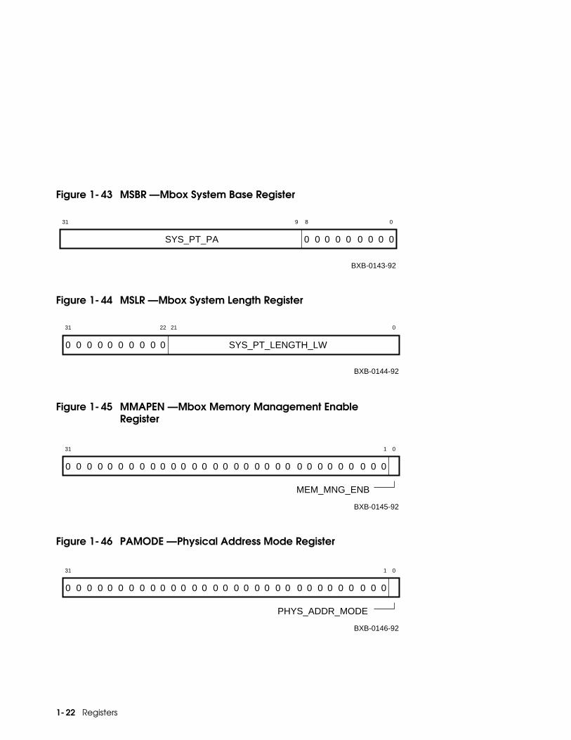
Figure 1-43 MSBR — Mbox System Base Register
Figure 1-44 MSLR — Mbox System Length Register
Figure 1-45 MMAPEN — Mbox Memory Management EnableRegister
Figure 1-46 PAMODE — Physical Address Mode Register
31 9 08
SYS_PT_PA 0 0 0 0 0 0 0 0 0
BXB-0143-92
31 22 21 0
0 0 0 0 0 0 0 0 0 0 SYS_PT_LENGTH_LW
BXB-0144-92
31 0
0 0 0 0 0 0 0 0 0 0 0 0 0 0 0 0 0 0 0 0 0 0 0 0 0 0 0 0 0 0 0
BXB-0145-92
MEM_MNG_ENB
1
31 0
0 0 0 0 0 0 0 0 0 0 0 0 0 0 0 0 0 0 0 0 0 0 0 0 0 0 0 0 0 0 0
BXB-0146-92
PHYS_ADDR_MODE
1

Registers 1-23
Figure 1-47 MMEADR — Memory Management ExceptionAddress Register
Figure 1-48 MMEPTE — Memory Management Exception PTEAddress Register
Figure 1-49 MMESTS — Memory Management Exception StatusRegister
31 0
BXB-0147-92
NME_FAULT_ADDR
31 0
BXB-0148-92
MIOD_FAULT_PTE_ADDR
31 29 28 26 25 16 15 14 13 3 012
SRC 0 0 0 0 0 0 0 0 0 0 0 0 0 0 0 0 0 0 0 0 0
BXB-0149-92
LOCK
FAULT M PTE_REF
LV

1-24 Registers
Figure 1-50 TBADR — Translation Buffer Parity Address Register
Figure 1-51 TBSTS — Translation Buffer Parity Status Register
Figure 1-52 PCADR — P-Cache Parity Address Register
31 0
BXB-0150-92
VA_TB_PE
31 29 28 9 8 4 3 06 5 12
SRC 0 0 0 0 0 0 0 0 0 0 0 0 0 0 0 0 0 0 CMD
BXB-0151-92
EM_VAL TPERR DPERR
LOCK
00
31 3 012
PC_PE_PA 0 0 0
BXB-0152-92

Registers 1-25
Figure 1-53 PCSTS — P-Cache Status Register
Figure 1-54 PCCTL — P-Cache Control Register
31 30 29 28 27 26 25 24 23 22 21 20 19 18 17 16 15 14 13 12 11 10 9 4 3 08
1
12
1 1 1 1 1 1 1 1 1 1 1 1 1 1 1 1 1 1 1 1
BXB-0153-92
LEFT_BANK RIGHT_BANK
DPERR LOCK
CMD
PTE_ER PTE_ER_WR
31 30 29 28 27 26 25 24 23 22 21 20 19 18 17 16 15 14 13 12 11 10 9 4 3 05
1
12
1 1 1 1 1 1 1 1 1 1 1 1 1 1 1 1 1 1 1
BXB-0154-92
PC_PE_ENB BANK_SEL
FORCE_HIT I_STR_ENB
D_STR_ENB
PMM
RED_ENB ELEC_DISABLE
1
8 7
1

1-26 Registers
Table 1-4 Gbus Registers
Register Address
Gbus$WHAMI F700 0000
Gbus$LEDs F700 0040
Gbus$PMask F700 0800
Gbus$Intr F700 00C0
Gbus$Halt F700 0100
Gbus$LSBRST F700 0140
Gbus$Misc F700 0180
Gbus$RMode_ENA F780 0000
Registers 1-27
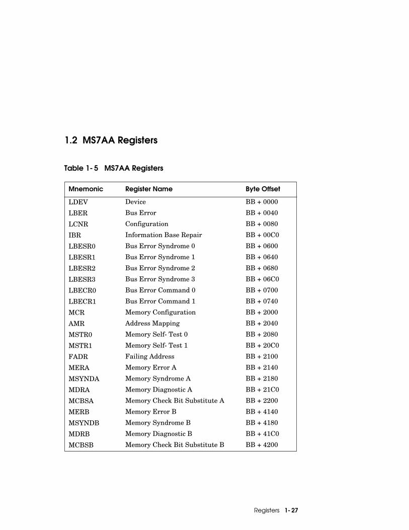
1.2 MS7AA Registers
Table 1-5 MS7AA Registers
Mnemonic Register Name Byte Offset
LDEV Device BB + 0000
LBER Bus Error BB + 0040
LCNR Configuration BB + 0080
IBR Information Base Repair BB + 00C0
LBESR0 Bus Error Syndrome 0 BB + 0600
LBESR1 Bus Error Syndrome 1 BB + 0640
LBESR2 Bus Error Syndrome 2 BB + 0680
LBESR3 Bus Error Syndrome 3 BB + 06C0
LBECR0 Bus Error Command 0 BB + 0700
LBECR1 Bus Error Command 1 BB + 0740
MCR Memory Configuration BB + 2000
AMR Address Mapping BB + 2040
MSTR0 Memory Self-Test 0 BB + 2080
MSTR1 Memory Self-Test 1 BB + 20C0
FADR Failing Address BB + 2100
MERA Memory Error A BB + 2140
MSYNDA Memory Syndrome A BB + 2180
MDRA Memory Diagnostic A BB + 21C0
MCBSA Memory Check Bit Substitute A BB + 2200
MERB Memory Error B BB + 4140
MSYNDB Memory Syndrome B BB + 4180
MDRB Memory Diagnostic B BB + 41C0
MCBSB Memory Check Bit Substitute B BB + 4200

1-28 Registers
Figure 1-55 LDEV — Device Register
Figure 1-56 LBER — Bus Error Register
31 0
DREV
BXB-0100-92
30 1516
DTYPE
31 18 17 16 15 14 13 12 11 10 9 4 3 08 7 6 5 12
RSVD
NSES CTCE DTCE
CDPE CPE2 CPE CE2
CNFE STE TDE
CDPE2
DIE SHE CAE
NXAE
19
BXB-0101-92
<3> <2> <1> <0>
<7> <6> <5> <4>
<11> <10> <9> <8>
<15> <14> <13> <12>
<18> <17> <16>
CE UCE2 UCE
E

Registers 1-29
Figure 1-57 LCNR — Configuration Register
Figure 1-58 IBR — Information Base Repair Register
Figure 1-59 LBESR0–3 — Bus Error Syndrome Registers
31 30 29 28 27 0
RSTSTATNHALTNRSTSTF
BXB-0102-92
CEEN
MBZ
1
31 3 012
MBZ
BXB-0218-92
SCLK XMT_SDAT RCV_SDAT
31 0
SYND_0
7 6
RSVD
SYND_1RSVD
SYND_2RSVD
SYND_3RSVD
BXB-0105-92
1-30 Registers
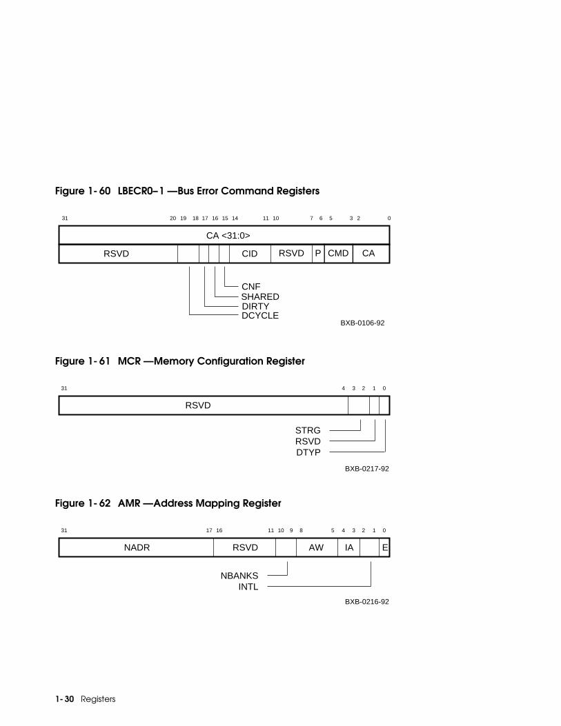
Figure 1-60 LBECR0–1 — Bus Error Command Registers
Figure 1-61 MCR — Memory Configuration Register
Figure 1-62 AMR — Address Mapping Register
31 20 19 18 17 16 15 14 11 10 0
CA <31:0>
7 6
RSVD CID
BXB-0106-92
RSVD P CMD CA
CNF
DIRTYSHARED
DCYCLE
5 3 2
31 4 3 012
RSVD
BXB-0217-92
STRG RSVD DTYP
31 17 16 11 10 9 4 3 08 5 12
NADR RSVD IA �E
BXB-0216-92
NBANKS INTL
AW

Registers 1-31
Figure 1-63 MSTR0–1 — Memory Self-Test Registers
Figure 1-64 FADR — Failing Address Register
Figure 1-65 MERA — Memory Error Register A
31 0
MSTR0
31 0
MSTR1
BXB-0215-92
31 0
FADR
BXB-0214-92
31 12 11 10 9 4 3 08 7 6 5 12
BXB-0219 -92
UCERB UCERA BNKER
FSTR
CERB CERA
APER MULE UCER
CER
RSVD

1-32 Registers
Figure 1-66 MSYNDA — Memory Syndrome Register A
Figure 1-67 MDRA — Memory Diagnostic Register A
Figure 1-68 MCBSA — Memory Check Bit Substitute Register A
31 08 7
RSVD SYNDA
BXB-0223-92
31 30 29 28 27 26 10 9 4 3 08 7 6 5 12
BXB-0225-92
�DCRD BRFSH DRFSH
FCPE FRPE IGSB
MODE
RFR
STPM EXST BPAS
DWDCDRDC FCBS
RSVD
31 08 7
RSVD SCB_A
BXB-0221-92

Registers 1-33
Figure 1-69 MERB — Memory Error Register B
Figure 1-70 MSYNDB — Memory Syndrome Register B
Figure 1-71 MDRB — Memory Diagnostic Register B
31 4 3 012
BXB-0220 -92
APER MULE UCER
CER
RSVD
31 08 7
RSVD SYNDB
BXB-0224-92
31 4 3 08 7 6 5 12
BXB-0226-92
IGSB MODE STPM EXST
BPAS DWDC DRDC FCBS
RSVD

1-34 Registers
Figure 1-72 MCBSB — Memory Check Bit Substitute Register B
31 08 7
RSVD SCB_B
BXB-0222-92

Registers 1-35
1.3 I/O Port Registers
Table 1-6 I/O Port Registers
Mnemonic Register NamePhysicalAddress
SoftwareAddress
LDEV Device 50 0000 A00 0000
LBER Bus Error 50 0002 A00 0040
LCNR Configuration 50 0004 A00 0080
IBR Information Base Repair 50 0006 A00 00C0
LMMR0 Memory Mapping 0 50 0010 A00 0200
LMMR1 Memory Mapping 1 50 0012 A00 0240
LMMR2 Memory Mapping 2 50 0014 A00 0280
LMMR3 Memory Mapping 3 50 0016 A00 02C0
LMMR4 Memory Mapping 4 50 0018 A00 0300
LMMR5 Memory Mapping 5 50 001A A00 0340
LMMR6 Memory Mapping 6 50 001C A00 0380
LMMR7 Memory Mapping 7 50 001E A00 03C0
LBESR0 Bus Error Syndrome 0 50 0030 A00 0600
LBESR1 Bus Error Syndrome 1 50 0032 A00 0640
LBESR2 Bus Error Syndrome 2 50 0034 A00 0680
LBESR3 Bus Error Syndrome 3 50 0036 A00 06C0
LBECR0 Bus Error Command 0 50 0038 A00 0700
LBECR1 Bus Error Command 1 50 003A A00 0740
LILID0 Interrupt Level 0 IDENT 50 0050 A00 0A00
LILID1 Interrupt Level 1 IDENT 50 0052 A00 0A40
LILID2 Interrupt Level 2 IDENT 50 0054 A00 0A80
LILID3 Interrupt Level 3 IDENT 50 0056 A00 0AC0
LCPUMASK CPU Interrupt Mask 50 0058 A00 0B00

1-36 Registers
Table 1-6 I/O Port Registers (Continued)
Figure 1-73 IBR — Information Base Repair Register
Figure 1-74 LILID0–3 — Interrupt Level 0–3 IDENT Registers
Mnemonic Register Name PhysicalAddress
SoftwareAddress
LMBPR Mailbox Pointer 50 0060 A00 0C00
IPCNSE I/O Port Chip Node-SpecificError
50 0100 A00 2000
IPCVR I/O Port Chip Vector 50 0102 A00 2040
IPCMSR I/O Port Chip Mode Selection 50 0104 A00 2080
IPCHST I/O Port Chip Hose Status 50 0106 A00 20C0
IPCDR I/O Port Chip Diagnostic 50 0108 A00 2100
31 3 012
MBZ
BXB-0218-92
SCLK XMT_SDAT RCV_SDAT
31 0
Reserved
BXB-0107-92
30 1516
IDENT

Registers 1-37
Figure 1-75 LCPUMASK — CPU Interrupt Mask Register
Figure 1-76 LMBPR — Mailbox Pointer Register
Figure 1-77 IPCNSE — I/O Port Chip Node-Specific Error Register
Figure 1-78 IPCVR — I/O Port Chip Vector Register
31 16 15 12 11 4 3 0
CPU 0
8 7
MBZ CPU 1CPU 2CPU 3
BXB-0109-92
31 0
BXB-0110-92
5
Mailbox Address <37:6> MBZ
6
31 30 21 20 19 18 17 16 15 12 11 4 3 08 7
0 Reserved
MBX_TIP UP_HOSE_OFLOMULT_INTR_ERR
DN_VRTX_ERR UP_VRTX_ERR
IPC_IE UP_HIC_IE
INTR_NSES
BXB-112-92
UP_HOSE_PKT_ERR UP_HOSE_PAR_ERR
31 0
Reserved
BXB-0108-92
30 1516
Vector
1-38 Registers
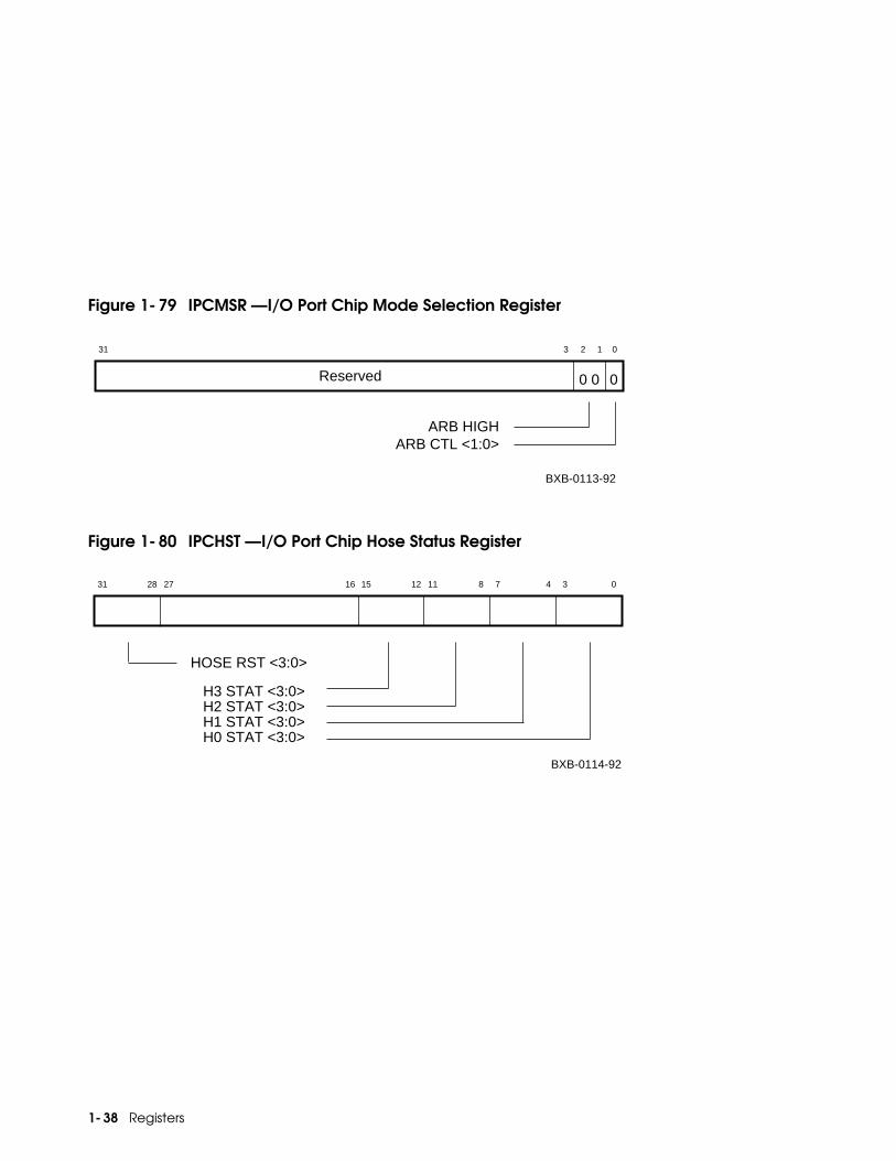
Figure 1-79 IPCMSR — I/O Port Chip Mode Selection Register
Figure 1-80 IPCHST — I/O Port Chip Hose Status Register
31 3 02 1
Reserved 0 0 0
ARB HIGH ARB CTL <1:0>
BXB-0113-92
31 28 27 16 15 12 11 4 3 08 7
BXB-0114-92
HOSE RST <3:0>
H3 STAT <3:0> H2 STAT <3:0> H1 STAT <3:0> H0 STAT <3:0>

Registers 1-39
Figure 1-81 IPCDR — I/O Port Chip Diagnostic Register
31 30 24 23 22 21 14 13 12 11 10 9 4 3 012
Reserved
BXB-0115-92
Reserved
DIS LSB CMD HIC LPBCK EN FRS DAT PE FRC CMD PE
FRC CNFE FRC CAE DIAG ECC <6:0> DIAG ECC EN
FRC DN DPE <1:0> FRS DN SEQ ERR FRC DN ILL CMD

1-40 Registers
1.4 DWLMA Registers
Table 1-7 LSB Registers
Figure 1-82 LDIAG — Diagnostic Register
Mnemonic Register Name Address
LDIAG Diagnostic BB + 40
IMSK Interrupt Mask BB + 44
LEVR Error Vector BB + 48
LERR Error BB + 4C
LGPR General Purpose BB + 50
IPR1 Interrupt Pending 1 BB + 54
IPR2 Interrupt Pending 2 BB + 58
IIPR Interrupt in Progress BB + 5C
31 28 27 26 25 24 23 22 21 20 19 18 17 16 15 14 13 12 11 10 9 08
RSVD
BXB-0209-92
Force CNF Err Disable Retries on NO ACK RSVD
DLLF AS
LOCK LOOP
STE Force XMI Access ASM0 ASM1
NODE
FRRM1 FRRM0
CRE FPE3 FPE0
FPE1 FPE2

Registers 1-41
Figure 1-83 IMSK — Interrupt Mask Register
Figure 1-84 LEVR — Error Vector Register
Figure 1-85 LERR — Error Register
31 28 27 26 25 24 23 22 21 20 19 18 17 16 15 14 13 12 4 3 07 6 5
BXB-0208-92
ITTO RSVD ICNAK IRER
ICC RSVD
IWEI IIPE
RSVD RSVD RSVD
IXPE IWSE
IRIDNAK
IMBER IRBDPE IDFDPE
IRSE INRR ICRD IWDNAK
31 16 15 0
RSVD VECTOR
BXB-0202-92DWLMA Error Interrupt Vector
31 30 29 28 27 19 18 15 14 13 12 11 4 3 07 6 5 2
BXB-0207-92
DHDPE XMIPE0 XMIPE1 XMIPE2
Data FIFO DPE RBDPE
MBOF FE
IVID MBPE MBIC MBIA
RSVDRSVDRSVD

1-42 Registers
Figure 1-86 LGPR — General Purpose Register
Figure 1-87 IPR1 — Interrupt Pending Register 1
Figure 1-88 IPR2 — Interrupt Pending Register 2
Figure 1-89 IIPR — Interrupt in Progress Register
31 0
LGPR
BXB-0203-92
31 28 27 24 23 20 19 16 15 12 11 4 3 08 7
IP8 IP7 IP6 IP5 IP4 IP3 IP2 IP1
BXB-0204-92
31 30 24 23 20 19 16 15 12 11 4 3 08 7
RSVD IP14 IP13 IP12 IP11 IP10 IP9
BXB-0205-92DWLMA Error Interrupt Pending
31 20 19 16 15 12 11 4 3 08 7
RSVD IDENTID IPL17ID IPL16ID IPL15ID IPL14ID
BXB-0206-92

Registers 1-43
Table 1-8 XMI Registers
Figure 1-90 XDEV — Device Register
Mnemonic Register Name Address
XDEV Device BB + 0000
XBER Bus Error BB + 0004
XFADR Failing Address BB + 0008
XFAER Failing Address Extension BB + 000C
IBR Information Base Repair BB + 0010
31 20 19 16 15 0
MBZ DREV Device Type
BXB-0233-92

1-44 Registers
Figure 1-91 XBER — Bus Error Register
31 30 29 28 27 26 25 24 23 22 21 20 19 18 17 16 15 14 13 12 11 10 9 4 3 0
FCID
BXB-0234-92
Commander Errors TTO RSVD CNAK RER RSE NRR CRD WDNAK
STF ETF NSES
Miscellaneous WEI XFAULT CC XBAD NHALT NRST ES
Responder Errors RIDNAK WSE PE IPE
2 1
EHWW DXTO
EMP RSVD

Registers 1-45
Figure 1-92 XFADR — Failing Address Register
Figure 1-93 XFAER — Failing Address Extension Register
Figure 1-94 IBR — Information Base Repair Register
31 30 29 0
FLN Failing Address
BXB-0235-92
31 28 27 26 25 16 15 0
CMD 0 0 ADDRESS EXTENSION MASK
BXB-0230-92
31 3 012
MBZ
BXB-0218-92
SCLK XMT_SDAT RCV_SDAT


Addressing 2-1
Chapter 2
AddressingThis chapter includes an overview of the VAX 7000 system and addressinginformation for the buses used in the system. Sections include:• VAX 7000 Block Diagram• LSB Address Space• XMI Addresses• VAXBI Addresses

2-2 Addressing
2.1 VAX 7000 Block Diagram
Figure 2-1 VAX 7000 Block Diagram
XMI
BXB-0054-92
MemoryProcessors
DEMNA DEMFA CIXCD KFMSA KDM70
CLOCKIOP DWLMA
LSB
DWMBB
Addressing 2-3
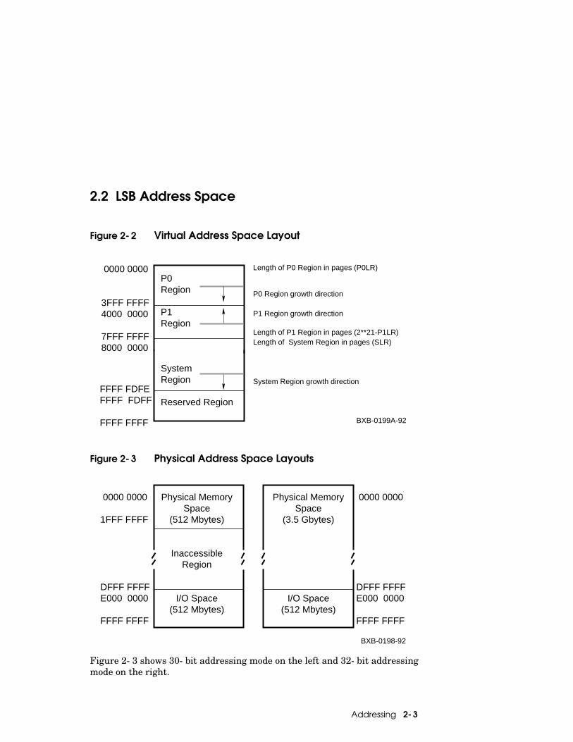
2.2 LSB Address Space
Figure 2-2 Virtual Address Space Layout
Figure 2-3 Physical Address Space Layouts
Figure 2-3 shows 30-bit addressing mode on the left and 32-bit addressingmode on the right.
0000 0000 3FFF FFFF 4000 0000 7FFF FFFF 8000 0000
P0 Region P1 Region System Region Reserved Region
BXB-0199A-92
Length of P0 Region in pages (P0LR)
P0 Region growth direction
P1 Region growth direction
Length of P1 Region in pages (2**21-P1LR)Length of System Region in pages (SLR)
System Region growth directionFFFF FDFE FFFF FDFF FFFF FFFF
0000 0000 1FFF FFFF DFFF FFFF E000 0000 FFFF FFFF
Physical Memory Space
(3.5 Gbytes)
I/O Space (512 Mbytes)
0000 0000 DFFF FFFF E000 0000 FFFF FFFF
Physical Memory Space
(512 Mbytes)
Inaccessible Region
I/O Space (512 Mbytes)
BXB-0198-92
2-4 Addressing
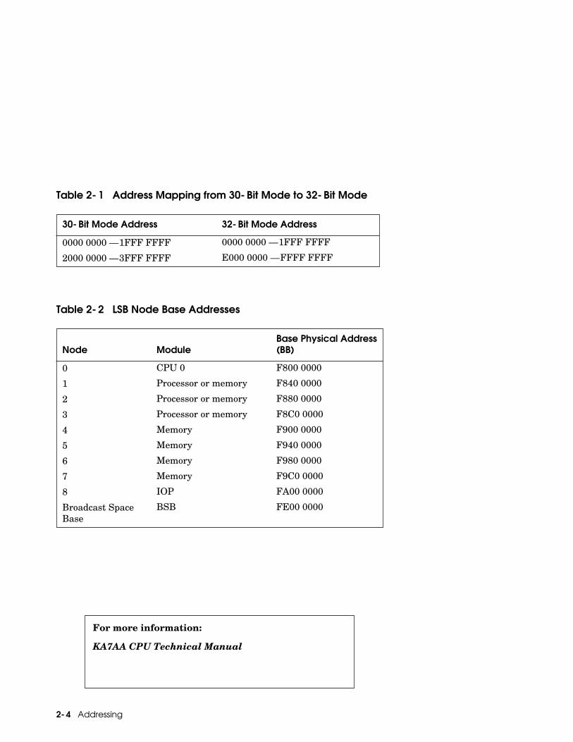
Table 2-1 Address Mapping from 30-Bit Mode to 32-Bit Mode
Table 2-2 LSB Node Base Addresses
30-Bit Mode Address 32-Bit Mode Address
0000 0000 — 1FFF FFFF 0000 0000 — 1FFF FFFF
2000 0000 — 3FFF FFFF E000 0000 — FFFF FFFF
Node ModuleBase Physical Address(BB)
0 CPU 0 F800 0000
1 Processor or memory F840 0000
2 Processor or memory F880 0000
3 Processor or memory F8C0 0000
4 Memory F900 0000
5 Memory F940 0000
6 Memory F980 0000
7 Memory F9C0 0000
8 IOP FA00 0000
Broadcast SpaceBase
BSB FE00 0000
For more information:
KA7AA CPU Technical Manual

Addressing 2-5
Table 2-3 Device Type Codes
Device Code (hex)
KA7AA 8002
MS7AA 4000
IOP 2000
DWLMA 102A
CIXCD 0C05
DEMFA 0823
DEMNA 0C03
DWMBB 2002
KDM70 0C22
KFMSA 0810
2-6 Addressing
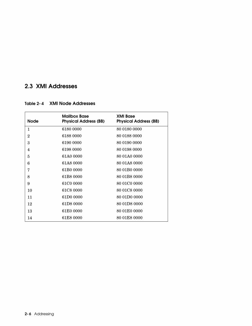
2.3 XMI Addresses
Table 2-4 XMI Node Addresses
NodeMailbox Base Physical Address (BB)
XMI Base Physical Address (BB)
1 6180 0000 80 0180 0000
2 6188 0000 80 0188 0000
3 6190 0000 80 0190 0000
4 6198 0000 80 0198 0000
5 61A0 0000 80 01A0 0000
6 61A8 0000 80 01A8 0000
7 61B0 0000 80 01B0 0000
8 61B8 0000 80 01B8 0000
9 61C0 0000 80 01C0 0000
10 61C8 0000 80 01C8 0000
11 61D0 0000 80 01D0 0000
12 61D8 0000 80 01D8 0000
13 61E0 0000 80 01E0 0000
14 61E8 0000 80 01E8 0000

Addressing 2-7
2.4 VAXBI Addresses
To examine a VAXBI register from the VAX 7000 console (see Example2-1), you need three pieces of information:1. The XMI number (0–3) to which the VAXBI bus is connected. 2. The base address of the VAXBI node (see Table 2-5).3. The offset of the VAXBI register to be examined (see Table 2-6).
The address of the register to be examined is expressed in this form:xmin:220xxyyy
where: n = the XMI numberxx = the base address of the VAXBI nodeyyy = the address offset of the VAXBI register
To calculate the address of the VAXBI register, add 2200 0000 plus thebase address of the VAXBI node (Table 2-5) plus the address offset of theVAXBI register (Table 2-6).
NOTE: You must look at the node ID plug on the backplane of the VAXBIcard cage to determine the node ID of the VAXBI option.
Example 2-1 Examining the Device Register of VAXBI Node 7
>>> e xmi1:2200E000xmi1: 2200E000 131C010E>>>

2-8 Addressing
Table 2-5 Base Addresses of VAXBI Nodes
Node ID Base Address
0 0000 0000
1 0000 2000
2 0000 4000
3 0000 6000
4 0000 8000
5 0000 A000
6 0000 C000
7 0000 E000
8 0001 0000
9 0001 2000
A 0001 4000
B 0001 6000
C 0001 8000
D 0001 A000
E 0001 C000
F 0001 E000

Addressing 2-9
Table 2-6 Address Offsets of VAXBI Registers
Mnemonic Register NameAddressOffset
DTYPE Device bb 1 + 00
VAXBICSR VAXBI Control and Status bb + 04
BER Bus Error bb + 08
EINTRSCR Error Interrupt Control bb + 0C
INTRDES Interrupt Destination bb + 10
IPINTRMSK IPINTR Mask bb + 14
FIPSDES Force-Bit IPINTR/STOP Destination bb + 18
IPINTRSRC IPINTR Source bb + 1C
SADR Starting Address bb + 20
EADR Ending Address bb + 24
BCICSR BCI Control and Status bb + 28
WSTAT Write Status bb + 2C
FIPSCMD Force-Bit IPINTR/STOP Command bb + 30
UINTRCSR User Interface Interrupt Control bb + 40
GPR0 General Purpose Register 0 bb + F0
GPR1 General Purpose Register 1 bb + F4
GPR2 General Purpose Register 2 bb + F8
GPR3 General Purpose Register 3 bb + FC
SOSR Slave-Only Status bb + 100
RXCD Receive Console Data bb + 200
1 bb is the base address of the VAXBI node (the address of the first location of thenodespace).

Console 3-1
Chapter 3
ConsoleThis chapter contains an overview of the console command set and com-mand syntax. It includes a section on device naming and examples of theuse of selected commands. Sections include:• Console Commands• Environment Variables• Device Name Fields• Command Syntax• Boot Command• Cdp Command• Show Configuration Command• Show Device Command• Show Network Command• Show Power Command

3-2 Console
3.1 Console Commands
Table 3-1 Console Commands
Command Description
boot Boot the operating system
build eeprom
Create a new EEPROM image
cdp Perform basic configuration management of DSSI devices
clear Clear the specified EEPROM option, remove a boot speci-fication environment variable, or clear the terminal screen
continue Resume processing at the point it was interrupted byCtrl/P
create Create an environment variable
deposit Store data in a specified location
examine Display contents of a memory location, a register, or a de-vice
help Provide basic information on the console commands whenthe system is in console mode
initialize Initialize the entire system or a specified device or subsys-tem
repeat Repeat a command; stop by entering Ctrl/C
set Record the current system configuration in the EEPROM,set the selected EEPROM option, modify an environmentvariable, or connect to another console or service
show Display the last saved configuration, device informationfor a disk or tape adapter, selected EEPROM information,current state of an environment variable, memory moduleinformation, information about network devices, or systempower status
start Begin execution of an instruction at specified address;does not initialize the system
stop Stop a specified processor

Console 3-3
Table 3-1 Console Commands (Continued)
Table 3-2 Boot Command Options
Command Description
test Test a specified device, a subsystem, or the entire system(default)
update Copy the contents of the EEPROM or FEPROMs on theboot processor to the EEPROM or FEPROMs on the speci-fied secondary processor(s)
# or ! Introduce a comment
Option Meaning
-file <file> Boot from the file <file>-flags <val> Boot flags that qualify the bootstrap. If omitted, the
value of the environment variable boot_flags is used.

3-4 Console
Table 3-3 Cdp Command Options
Table 3-4 Clear EEPROM Command Options
Option Meaning
-a Set device allocation class, allclass-i Select interactive mode; set all parameters
-n Set device node name, nodename (up to 16 characters)
-o Overridde warning messages
-u Set device unit number, unitnum-sa allclass Set allclass for all DSSI devices in the system to the
specified value
-sn Set nodename to either RFhscn or TFhscn
h is the device hose number (0–3)s is the device slot number (1–14)c is the device channel number (0, 1)n is the device node ID number (0–6)
-su unitnum
Set the starting unitnum for the first DSSI device inthe system to the specified value. Subsequent DSSI unitnumbers are incremented from this base.
Option Meaning
diag_sdd Remove from EEPROM failure information logged bysymptom-directed diagnosis
diag_tdd Remove from EEPROM failure information logged bytest-directed diagnosis
log Remove from EEPROM all failure information(symptom-directed diagnosis, test-directed diagnosis,and operating system)
symptom Remove from EEPROM all failure information on op-erating system

Console 3-5
Table 3-5 Create Command Option
Table 3-6 Deposit and Examine Command Options
Option Meaning
-nv Store the nonvolatile environment variable in EEPROM
Option Meaning
-b Define data size as a byte
-d Disassemble instruction at current address (examine command only)
-h Define data size as a hexword
-l Define data size as a longword; initial default
-o Define data size as an octaword
-q Define data size as a quadword
-w Define data size as a word
-n val Number of consecutive locations to modify
-s val Address increment size. Default is data size.
-u Allow access to console private memory, while dis-abling virtual address protection checks
space: Device name and address space, as follows:
<dev_name> Device name; for example, xmi0, ka7aa0, or demna0
gpr Define the address space as the general register set,R0 through R15. The data size is always a longword.
ipr Define the address space as the internal processorregisters (IPRs). The data size is always a longword.
psl Define the address space as the processor statuslongword (PSL).
pmem Define the address space as physical memory; initialdefault
vmem Define the address space as virtual memory. All ac-cess and protection checking occur.

3-6 Console
Table 3-7 Set EEPROM Command Options
Table 3-8 Set Host Command Options
Table 3-9 Show EEPROM Command Options
Option Meaning
field Record the LARS report number and comment
manufactur-ing
Record manufacturing information: module serialnumber, module part number, and module firmwarerevision
serial Record system serial number
Option Meaning
-bus b DSSI bus on which the node resides
-dup Remote node is a DUP server
Option Meaning
diag_sdd Display failure information logged by symptom-directed diagnosis
diag_tdd Display failure information logged by test-directed di-agnosis
field Display LARS number and comment
manufactur-ing
Display manufacturing information: module serialnumber, module part number, and module firmwarerevision
serial Display system serial number
symptom Display failure information logged on operating sys-tem

Console 3-7
Table 3-10 Show Power Command Options
Table 3-11 Test Command Options
Option Meaning
-h History status — the value of each parameter at the lastsystem shutdown
-s Current status (default)
main Power status of the main cabinet (default)
right Power status of the expander cabinet to the right of themain cabinet
left Power status of the expander cabinet to the left of themain cabinet
Option Meaning
-write Select writes to media as well as reads (read-only is thedefault). Applicable only to disk testing (ignored other-wise).
-nowrite<list>
Used with -write to prevent selected devices or groupsof devices from being written to
-omit <list> Specify device not to test; takes a single device or devicelist as a qualifier
-t <time> Run time in seconds for the test command; default forsystem is 600 seconds (10 minutes).
-q "Quiet" option prevents informational messages abouttesting start and stop from being displayed on the con-sole terminal. Error messages are always reported.

3-8 Console
Table 3-12 Update Command Options
Option Meaning
-flash Update the FEPROMs on the specified secondary proces-sor
-eeprom Update the EEPROM on the specified secondary proces-sor
For more information:
VAX 7000 Console Reference ManualVAX 7000 Advanced Troubleshooting

Console 3-9
3.2 Environment Variables
An environment variable is a name and a value association maintained bythe console program. The value associated with an environment variable isan ASCII string (up to 128 characters) or an integer. Volatile environmentvariables are initialized by a system reset; others are nonvolatile acrosssystem failures.Environment variables can be created, modified, displayed, and deleted us-ing the console create, set, show, and clear commands.
Table 3-13 Environment Variables
Variable Attribute Function
auto_action Nonvola-tile
The action the console will take followingan error halt. Values are:restart—Automatically restart. If restartfails, boot the operating system.boot—Automatically boot the operatingsystemhalt—Enter console mode (default)
baud Nonvola-tile
Sets the baud rate of the console terminalport to 300, 600, 1200, 2400, 4800, or 9600(default)
bootdef_dev Nonvola-tile
The default device or device list from whichbooting is attempted when the boot com-mand does not specify a device name
boot_file Nonvola-tile
The default file name used for the primarybootstrap when the boot command does notspecify a file name
boot_osflags Nonvola-tile
Additional parameters passed to the systemduring booting if none are specified by the -flags qualifier to the boot command
boot_reset Nonvola-tile
Resets system and displays self-test resultsduring booting. Default is off.
cpu Volatile Selects the current boot processor
3-10 Console
Table 3-13 Environment Variables (Continued)
Variable Attribute Function
cpu_enabled Nonvola-tile
A bitmask indicating which processors areenabled to run (leave console mode). If notdefined, all processors are considered en-abled. Default is 0xFF.
cpu_primary Nonvola-tile
A bitmask indicating which processors areenabled to become the next boot processorafter the next reset. If not defined, allavailable processors are considered en-abled. Default is 0xFF.
d_harderr Volatile Determines action taken following a harderror. Values are halt (default) and con-tinue. Applies only when using the testcommand.
d_report Volatile Determines level of information providedby the diagnostic reports. Values are sum-mary (default) and full. Applies onlywhen using the test command.
d_softerr Volatile Determines action taken following a softerror. Values are continue (default) andfull. Applies only when using the testcommand.
enable_audit Nonvola-tile
When set to on, allows audit trail mes-sages to be displayed during booting.
interleave Nonvola-tile
The memory interleave specification. Val-ues must be default, none, or an explicitinterleave list. Default value is default.
language Nonvola-tile
Determines whether system displays mes-sage numbers or message text in English(default).
For more information:
VAX 7000 Console Reference Manual
Console 3-11
3.3 Device Name Fields
Device names are used in several console commands. A device name is ex-pressed in the form ddccuuuu.node.channel.slot.hose. Fields are sepa-rated by periods. Table 3-14 lists the field definitions.
Table 3-14 Device Name Fields
Field Size Definition
dd 2 Protocol used to access the device:
du MSCP disk (CI, SI, DSSI)
mu MSCP tape (CI, SI, DSSI)
ex XMI Ethernet
fx XMI FDDI
cc 2 (max) Controller letter (a–zz) assigned by console,based on the system configuration
uuuu 4 (max) Unit number of the device (0–9999) determinedby the I/O channel number and the XMI slotnumber of the adapter
node 3 (max) Node number (0–255) of the device on a remote(CI or DSSI) bus. If the remote bus is a CI, this isthe CI node number of the HSC; if it is a DSSI,this is the node number of the disk.
channel 1 Channel number (0–1); used only if the adapteris a KFMSA
slot 2 (max) XMI slot number (1–14) of the adapter
hose 1 Hose number (0–3) that connects to the XMI bus
For more information:
VAX 7000 Console Reference ManualVAX 7000 Operations Manual

3-12 Console
3.4 Command Syntax
b[oot] [-fl[ags] <parameters>] [-fi[le] <filename>] <device_name>bu[ild] ee[prom]cdp [-{a,i,n,o,u}] [-sn] [-sa <val>] [<dssi_device>]cl[ear] ee[prom] <option>cl[ear] <envar>cl[ear] sc[reen]c[ontinue]cr[eate] [-nv] <envar> [<value>]d[eposit] [-{b,w,l,q,o,h,u}] [{-n val, -s val}] [<space>:]<adrs> <data>e[xamine] [-{b,w,l,q,o,h,d,u}] [{-n val, -s val}] [<space>:]<adrs> h[elp] [<option>]i[nitialize] [<device_name>]r[epeat] [<command>]se[t] c[onfiguration]se[t] ee[prom] [<option>]se[t] <envar> [<value>]se[t] h[ost] [-dup] [-bus <b>] node [<task>]sh[ow] c[onfiguration]sh[ow] dev[ice] [<dev_name>]sh[ow] ee[prom] [<option>]sh[ow] <envar>sh[ow] m[emory]sh[ow] ne[twork]sh[ow] power [{-h, -s}] [{main, right, left}]s[tart] <address>sto[p] <cpu_device_name>t[est] [-write] [-nowrite <list>] [-omit <list>] [-t <time>] [-q] [<dev_arg>]upd[ate] [-{e[eprom], f[lash]}] [<device_name>]

Console 3-13
Table 3-15 Console Special Characters
Character Function
Return Carriage return; ends a command line
Backslash Line continuation
X Delete key; deletes previously typed character
Help By itself, displays first-level help. When pressed afterpart of a command, displays options available.
Ctrl/A, F14 Toggles between insertion and overstrike modes
Ctrl/B, ⇑ Recall previous command
Ctrl/C Terminate running process
Ctrl/D, ⇐ Move cursor left one position
Ctrl/E Move cursor to end of line
Ctrl/F, ⇒ Move cursor right one position
Ctrl/H, BS, F12 Move cursor to beginning of line
Ctrl/J Delete word
Ctrl/O Stop output to console terminal for current command.Toggles between enable and disable.
Ctrl/P In console mode, acts like Ctrl/C. In program mode,causes the boot processor to halt and begin runningthe console program.
Ctrl/Q Resume output to console terminal
Ctrl/R Redisplay the current line
Ctrl/S Stop output to console terminal
Ctrl/U Delete entire line
* Wildcarding for some commands
" " Quotes for set environment variable name
#, ! Comment specifier
For more information:
VAX 7000 Console Reference ManualVAX 7000 Advanced Troubleshooting

3-14 Console
3.5 Boot Command
Example 3-1 Boot Command — Booting from an InfoServer
>>> show network polling for units on demna0, slot 3, xmi0...exa0.0.0.3.0 08-00-2B-0B-BB-ED >>> boot exa0 -file ISL_LVAX_BL10 Initializing...F E D C B A 9 8 7 6 5 4 3 2 1 0 NODE # A M . . . . . P P TYP o + . . . . . + + ST1 . . . . . . . E B BPD o + . . . . . + + ST2 . . . . . . . E B BPD + + . . . . . + + ST3 . . . . . . . E B BPD
. . . . + . + . . . . + . + C0 XMI + . . . . . . . . . . . . . . C1 . . . . . . . . . . . . . . C2 . . . . . . . . . . . . . . C3
. A0 . . . . . . . ILV .128 . . . . . . . 128MbFirmware Rev = V1.0-1625 SROM Rev = V1.0-0 SYS SN = GAO1234567 Booting...Connecting to boot device exa0 -file ISL_LVAX_BL10Created boot device: exa0.0.0.3.0Resulting file is mopd1:ISL_LVAX_BL10/exa0.0.0.3.0.....Load complete!Network Initial System Load Function Version 1.1FUNCTION FUNCTION ID 1 - Display Menu 2 - Help 3 - Choose Service 4 - Select Options 5 - StopEnter a function ID value: 3 OPTION OPTION ID 1 - Find Services 2 - Enter known Service NameEnter an Option ID value: 1 WorkingServers found: 2

Console 3-15
Example 3-1 Boot Command — Booting from an InfoServer(Continued)
Service Name Format: Service Number Service Name Server Name Ethernet ID#1VMS054ESS_08002B0BBBED08-00-2B-0B-BB-ED#2CD_BIN_83371ESS_08002B0BBBED08-00-2B-0B-BB-ED#1INFO3$RZ57INFO308-00-2B-26-A6-98#2CD_DOC_0050INFO308-00-2B-16-04-98Enter a Service number or <CR> for more: 1 [operating system banner appears]
3-16 Console
Table 3-16 Sample Boot Commands
Boot From Sample Boot Command
Local device boot dua2.2.0.1.0InfoServer onEthernet
boot exa0 -file ISL_LVAX_BL10
InfoServer onFDDI
boot fxa0 -file ISL_LVAX_BL10
CI VAXcluster boot -fl 0,4,0 dua20.14.0.2.0Shadow set b -fl 8DAC,2,0 dua3500.14.0.12.1, dua63.14.0.12.1DSSI VAXclus-ter
boot -flags 0,3,0 dub1.1.0.6.0
For more information:
VAX 7000 Console Reference ManualVAX 7000 Operations Manual

Console 3-17
3.6 Cdp Command
Example 3-2 Cdp Command
>>> show devicepolling for units on kfmsa0, slot 0, xmi0...dua5.0.0.13.0 BASHFL$DIA5 RF71polling for units on cixcd0, slot 14, xmi1...dub44.1.0.13.0 $1$DIA44 (BLANK4) RF71
>>> cdp -i ! Interactive modedua5.0.0.13.0:Node Name [BASHFL]? ! Press Return to go to nextAllocation Class [0]? ! field without making aUnit Number [5]? ! change.dub44.1.0.13.0:Node Name [BLANK4]?Allocation Class [1]Unit Number [44]? ! Press Return to exit.
>>> cdp -n dua5 ! Set device node name of dua5.dua5.0.0.13.0:Node Name [BASHFL]? ! Exit, no changes made.
>>> cdp -a ! Set device allocation class.dua5.0.0.13.0:Allocation Class [0]?dub44.1.0.13.0:Allocation Class [1]? ! Exit, no changes made.
For more information:
VAX 7000 Console Reference Manual

3-18 Console
3.7 Show Configuration Command
Example 3-3 Show Configuration Command
>>> show config
Name Type Rev MnemonicLSB0+ KA7AA (8002) 0000 ka7aa0 1+ MS7AA (4000) 0000 ms7aa07+ MS7AA (4000) 0000 ms7aa18+ IOP (2000) 0001 iop0
C0 XMI xmi08+ DWLMA (102A) 0104 dwlma0C+ KDM70 (0C22) 1E11 kdm700E+ DEMNA (0C03) 0802 demna0
C1 XMI xmi12+ KFMSA (0810) A2A6 kfmsa03+ DEMNA (0C03) 0802 demna18+ DWLMA (102A) 0104 dwlma1A+ CIXCD (0C05) 4611 cixcd0C+ KDM70 (0C22) 1E11 kdm701
For more information:
VAX 7000 Console Reference Manual

Console 3-19
3.8 Show Device Command
Example 3-4 Show Device Command
>>> show devicepolling for units on kfmsa0, slot 1, xmi0...dub1.1.1.1.2 RF3101$DIA1 RF72dub3.3.1.1.2 RF3103$DIA3 RF72polling for units on kdm700, slot 11, xmi0...duc1.0.0.11.2 DUC1 RA70duc2.0.0.11.2 DUC2 RA70duc3.0.0.11.2 DUC3 RA70duc213.0.0.11.2 DUC213 RA82>>>
For more information:
VAX 7000 Console Reference Manual
3-20 Console
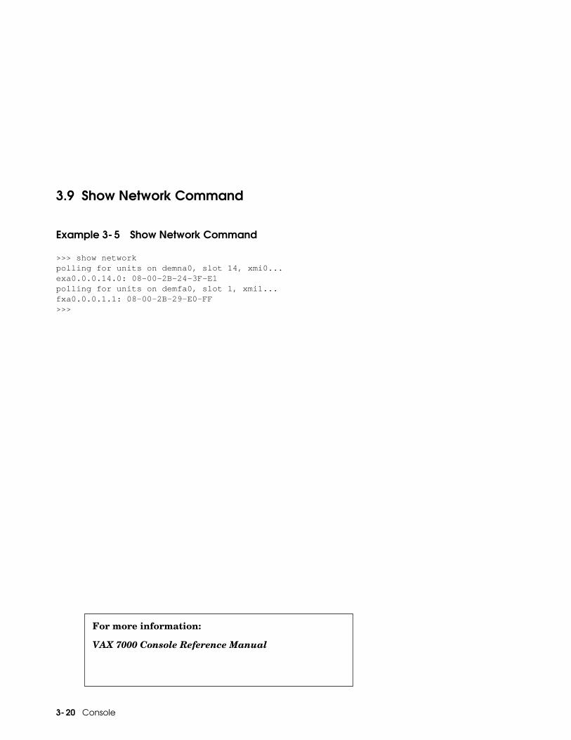
3.9 Show Network Command
Example 3-5 Show Network Command
>>> show networkpolling for units on demna0, slot 14, xmi0...exa0.0.0.14.0: 08-00-2B-24-3F-E1polling for units on demfa0, slot 1, xmi1...fxa0.0.0.1.1: 08-00-2B-29-E0-FF>>>
For more information:
VAX 7000 Console Reference Manual

Console 3-21
3.10 Show Power Command
Example 3-6 Show Power Command
>>> show powerCabinet: Main Regulator : A B C------------------------------------------------------------------------------- Primary Micro Firmware Rev : 2.0 2.0 2.0 Secondary Micro Firmware Rev : 2.0 2.0 2.0 Power Supply State : NORMAL NORMAL BBU MODE AC Line Voltage (V RMS) : 113.71 114.35 115.93 DC Bulk Voltage (VDC) : 227.02 227.02 227.02 48V DC Bus Voltage (VDC) : 47.57 47.57 47.57 48V DC Bus Current (ADC) : 30.17 29.68 29.58 48V Battery Pack Voltage (VDC) : 50.85 50.72 47.91 24V Battery Pack Votlage (VDC) : 25.56 25.56 23.95 Battery Pack Charge Current (IDC) : 2.91 2.90 0 Ambient Temperature (Degree C) : 26.22 24.80 24.75 Elapsed Time (Hours) : 290.00 290.00 290.00Remaining Battery Capacity (Minutes) : 8.00 8.00 8.00 Battery Cutoff Counter (Cycles) : 0 1.00 1.00 Battery Configuration : 4 Batteries 4 Batteries 4 Batteries Heatsink Status : NORMAL NORMAL NORMAL Battery Pack Status : CHARGING CHARGING DISCHG’G Last UPS Test Status : PASSED PASSED TESTING LDC POWER Status : 0 PIU Primary Status : 0 PIU Secondary Status : 0
The cabinet in Example 3-6 has three power regulators. If the cabinet hasfewer than three regulators, the appropriate column (A, B, or C) is leftblank. The bottom three lines of the output, showing PIU power status,apply only to the main cabinet.Table 3-17 lists the abbreviations used in four lines of the Show Powercommand: Power Supply State, Heatsink Status, Battery Pack Status,and Last UPS Test Status.
For more information:
VAX 7000 Console Reference Manual

3-22 Console
Table 3-17 Abbreviations Used in Show Power Command Output
Abbreviation Meaning
Power Supply StateNORMAL Normal AC operation
BBU MODE UPS mode
BRKR OPEN Breaker open
NO AC IN No AC voltage
KEYSW OFF Keyswitch off
NON FATAL Nonfatal fault
FATAL Fatal fault
SPARE
Heatsink StatusBROKEN Broken
FAULT Fault (red zone)
WARNING Warning
NORMAL Normal operation
Battery Pack StatusNO BATTERY Battery pack not installed
BATT FLT Battery pack failure
BBU INH UPS inhibit
CHG INH Charger inhibit
BATT EOL Battery at end of life
DISCHARG Battery discharged
DISCHG’G Discharging
CHARGING Charging
OVER 24HRS Charge mode longer than 24 hours
FULL CHG’D Fully charged

Console 3-23
Table 3-17 Abbreviations Used in Show Power Command Output(Continued)
Abbreviation Meaning
Last UPS Test StatusNO BATTER Battery pack not installed
NOT READY Battery pack not ready (only if test requested)
ABORTED Test aborted
TESTING Test in progress
FAILED Test failed
PASSED Test passed

Diagnostics 4-1
Chapter 4
DiagnosticsDiagnostics are run using console commands. This chapter contains exam-ples of diagnostic sessions. Sections include:• Test Command• Set Host Command — Running DUP-Based Diagnostics and Utilities• Set Host Command — Running Diagnostics on a Remote XMI Adapter

4-2 Diagnostics
4.1 Test Command
Example 4-1 Test Command — System Test
>>> test -t 120Configuring system...Default system exerciser selected for run time of 120 secondsType Ctrl/C to abort
Starting floating point exerciser on ka7aa0 (id #57)Starting floating point exerciser on ka7aa1 (id #58)Starting memory exerciser, running on ka7aa0 (id #59)Starting memory exerciser, running on ka7aa1 (id #60)Starting multiprocessor exerciser on ka7aa* (id #61)Starting network exerciser on exa0.0.0.4.0 in internal mode (id #62)Starting network exerciser on exb0.0.0.5.0 in external mode (id #63)Starting network exerciser on exc0.0.0.4.1 in external mode (id #64)Starting network exerciser on fxa0.0.0.2.1 in external mode (id #65)Starting network exerciser on fxb0.0.0.3.2 in external mode (id #66)Starting device exerciser on dua10.14.0.1.0 (id #67)Starting device exerciser on dub0.15.0.2.0 (id #68)Starting device exerciser on duc0.0.0.3.0 (id #69)Starting device exerciser on dud0.0.0.E.0 (id #70)Starting device exerciser on dua11.14.0.1.0 (id #71)Starting device exerciser on dub1.15.0.2.0 (id #72)Starting device exerciser on duc1.1.0.3.0 (id #73)Starting device exerciser on dud1.1.0.E.0 (id #74)Starting device exerciser on dua12.14.0.1.0 (id #75)Starting device exerciser on dub2.15.0.2.0 (id #76)Starting device exerciser on dua13.14.0.1.0 (id #77)Starting device exerciser on dub19.15.0.2.0 (id #78)Stopping device exerciser on dua10.14.0.1.0 (id #67)Stopping device exerciser on dub0.15.0.2.0 (id #68)Stopping device exerciser on duc0.0.0.3.0 (id #69)Stopping device exerciser on dud0.0.0.E.0 (id #70)Stopping device exerciser on dua11.14.0.1.0 (id #71)Stopping device exerciser on dub1.15.0.2.0 (id #72)Stopping device exerciser on duc1.1.0.3.0 (id #73)Stopping device exerciser on dud1.1.0.E.0 (id #74)Stopping device exerciser on dua12.14.0.1.0 (id #75)Stopping device exerciser on dub2.15.0.2.0 (id #76)Stopping device exerciser on dua13.14.0.1.0 (id #77)Stopping device exerciser on dub3.15.0.2.0 (id #78)Starting device exerciser on dua20.14.0.1.0 (id #79)Starting device exerciser on dub4.15.0.2.0 (id #80)Starting device exerciser on dua21.14.0.1.0 (id #81)Starting device exerciser on dub5.15.0.2.0 (id #82)Starting device exerciser on dua22.14.0.1.0 (id #83)Starting device exerciser on dub6.15.0.2.0 (id #84)Starting device exerciser on dua23.14.0.1.0 (id #85)

Diagnostics 4-3
Example 4-1 Test Command — System Test (Continued)
Starting device exerciser on dua30.14.0.1.0 (id #86)Test time has expired...
Stopping floating point exerciser on ka7aa0 (id #57)Stopping floating point exerciser on ka7aa1 (id #58)Stopping memory exerciser on ka7aa0 (id #59)Stopping memory exerciser on ka7aa1 (id #60)Stopping multiprocessor exerciser (id #61)Stopping network exerciser on exa0.0.0.4.0 (id #62)Stopping network exerciser on exb0.0.0.5.0 (id #63)Stopping network exerciser on exc0.0.0.4.1 (id #64)Stopping network exerciser on fxa0.0.0.2.1 (id #65)Stopping network exerciser on fxb0.0.0.3.2 (id #66)Stopping device exerciser on dua20.14.0.1.0 (id #79)Stopping device exerciser on dub4.15.0.2.0 (id #80)Stopping device exerciser on dua21.14.0.1.0 (id #81)Stopping device exerciser on dub5.15.0.2.0 (id #82)Stopping device exerciser on dua22.14.0.1.0 (id #83)Stopping device exerciser on dub6.15.0.2.0 (id #84)Stopping device exerciser on dua23.14.0.1.0 (id #85)Stopping device exerciser on dua30.14.0.1.0 (id #86)Done testing...
The following devices were not tested:
dua36.14.0.1.0 dua37.14.0.1.0 dua38.14.0.1.0 . . dua77.15.0.1.0
>>>

4-4 Diagnostics
Example 4-2 Test Command — Write/Read/Compare Test of AllDisks Not Associated with Controller "a"
>>> test -nowrite "dua*" -write -t 120Configuring system...Default system exerciser selected for run time of 120 secondsType Ctrl/C to abort
You have selected destructive testing of the following devices: dub0.0.0.2.0 dub1.1.0.2.0 dub2.2.0.2.0 dub3.3.0.2.0 duc0.0.0.3.0 duc1.1.0.3.0 dud0.0.0.E.0 dud1.1.0.E.0
Are you sure you want to perform writes to these disks? [yes/(no)] yesUser data on all selected devices may be lost. Continue? [yes/(no)] yes
Testing...
Starting floating point exerciser on ka7aa0 (id #213)Starting floating point exerciser on ka7aa1 (id #214)Starting memory exerciser, running on ka7aa0 (id #215)Starting memory exerciser, running on ka7aa1 (id #216)Starting multiprocessor exerciser on ka7aa* (id #217)Starting network exerciser on exa0.0.0.4.0 in internal mode (id #218)Starting network exerciser on exb0.0.0.5.0 in external mode (id #219)Starting network exerciser on exc0.0.0.4.1 in external mode (id #220)Starting network exerciser on fxa0.0.0.2.1 in external mode (id #221)Starting network exerciser on fxb0.0.0.3.2 in external mode (id #222)Starting device exerciser on dua10.14.0.1.0 (id #223)Starting device exerciser in DESTRUCT mode on dub0.15.0.2.0 (id 224)Starting device exerciser in DESTRUCT mode on duc0.0.0.3.0 (id #225)Starting device exerciser in DESTRUCT mode on dud0.0.0.E.0 (id #226)Starting device exerciser on dua11.14.0.1.0 (id #227)Starting device exerciser in DESTRUCT mode on dub1.15.0.2.0 (id #228)Starting device exerciser in DESTRUCT mode on duc1.1.0.3.0 (id #229)Starting device exerciser in DESTRUCT mode on dud1.1.0.E.0 (id #230)Starting device exerciser on dua12.14.0.1.0 (id #231)Starting device exerciser in DESTRUCT mode on dub2.15.0.2.0 (id #232)Starting device exerciser on dua13.14.0.1.0 (id #233)Starting device exerciser in DESTRUCT mode on dub3.15.0.2.0 (id #234)Stopping device exerciser on dua10.14.0.1.0 (id #223)Stopping device exerciser on dub0.15.0.2.0 (id #224)Stopping device exerciser on duc0.0.0.3.0 (id #225)Stopping device exerciser on dud0.0.0.E.0 (id #226)Stopping device exerciser on dua11.14.0.1.0 (id #227)

Diagnostics 4-5
Example 4-2 Test Command — Write/Read/Compare Test of AllDisks Not Associated with Controller "a" (Contin-ued)
Stopping device exerciser on dub1.15.0.2.0 (id #228)Stopping device exerciser on duc1.1.0.3.0 (id #229)Stopping device exerciser on dud1.1.0.E.0 (id #230)Stopping device exerciser on dua12.14.0.1.0 (id #231)Stopping device exerciser on dub2.15.0.2.0 (id #232)Stopping device exerciser on dua13.14.0.1.0 (id #233)Stopping device exerciser on dub3.15.0.2.0 (id #234)Starting device exerciser on dua20.14.0.1.0 (id #235)Starting device exerciser in DESTRUCT mode on dub4.15.0.2.0 (id #236)Starting device exerciser on dua21.14.0.1.0 (id #237)Starting device exerciser in DESTRUCT mode on dub5.15.0.2.0 (id #238)Starting device exerciser on dua22.14.0.1.0 (id #239)Starting device exerciser in DESTRUCT mode on dub6.15.0.2.0 (id #240)Starting device exerciser on dua23.14.0.1.0 (id #241)Starting device exerciser on dua30.14.0.1.0 (id #242)Test time has expired...
Stopping floating point exerciser on ka7aa0 (id #213)Stopping floating point exerciser on ka7aa1 (id #214)Stopping memory exerciser on ka7aa0 (id #215)Stopping memory exerciser on ka7aa1 (id #216)Stopping multiprocessor exerciser (id #217)Stopping network exerciser on exa0.0.0.4.0 (id #218)Stopping network exerciser on exb0.0.0.5.0 (id #219)Stopping network exerciser on exc0.0.0.4.1 (id #220)Stopping network exerciser on fxa0.0.0.2.1 (id #221)Stopping network exerciser on fxb0.0.0.3.2 (id #222)Stopping device exerciser on dua20.14.0.1.0 (id #235)Stopping device exerciser on dub4.15.0.2.0 (id #236)Stopping device exerciser on dua21.14.0.1.0 (id #237)Stopping device exerciser on dub5.15.0.2.0 (id #238)Stopping device exerciser on dua22.14.0.1.0 (id #239)Stopping device exerciser on dub6.15.0.2.0 (id #240)Stopping device exerciser on dua23.14.0.1.0 (id #241)Stopping device exerciser on dua30.14.0.1.0 (id #242)Done testing...
>>>

4-6 Diagnostics
Example 4-3 Test Command — Destructive Exercising Selected,Then Aborted
>>> test -w -n "dua*"Configuring system...Default system exerciser selected for run time of 600 secondsType Ctrl/C to abort
You have selected destructive testing of the following devices:
dub0.0.0.2.0 dub1.1.0.2.0 dub2.2.0.2.0 dub3.3.0.2.0 duc0.0.0.3.0 duc1.1.0.3.0 dud0.0.0.E.0 dud1.1.0.E.0
Are you sure you want to perform writes to these disks? [yes/(no)] no
Testing aborted...
>>>
Example 4-4 Output from Test Command — Quiet Qualifier Set
>>> test -q -t 300Configuring system...Default system exerciser selected for run time of 300 secondsType Ctrl/C to abort
Done testing...
>>>
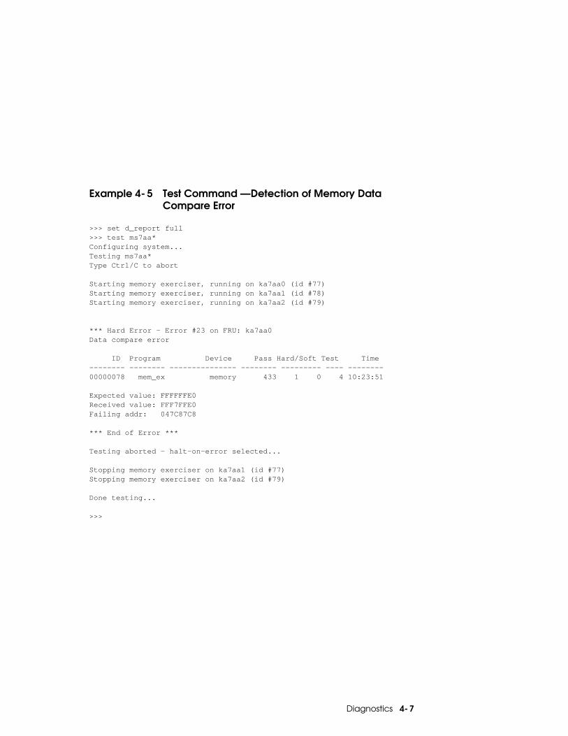
Diagnostics 4-7
Example 4-5 Test Command — Detection of Memory DataCompare Error
>>> set d_report full>>> test ms7aa*Configuring system...Testing ms7aa*Type Ctrl/C to abort
Starting memory exerciser, running on ka7aa0 (id #77)Starting memory exerciser, running on ka7aa1 (id #78)Starting memory exerciser, running on ka7aa2 (id #79)
*** Hard Error - Error #23 on FRU: ka7aa0Data compare error
ID Program Device Pass Hard/Soft Test Time-------- -------- --------------- -------- --------- ---- --------00000078 mem_ex memory 433 1 0 4 10:23:51
Expected value: FFFFFFE0Received value: FFF7FFE0Failing addr: 047C87C8
*** End of Error ***
Testing aborted - halt-on-error selected...
Stopping memory exerciser on ka7aa1 (id #77)Stopping memory exerciser on ka7aa2 (id #79) Done testing...
>>>

4-8 Diagnostics
Example 4-6 Test Command — Use of Wildcard
>>> test dem*a*Configuring system...Testing dem*a*Type Ctrl/C to abort Initializing DEMNA0Initializing DEMNA1Initializing DEMFA0DEMNA0 self-test passedDEMNA1 self-test passedDEMFA0 self-test passedStarting network exerciser on exa0.0.0.4.0 in internal mode (id #144)Starting network exerciser on exb0.0.0.5.0 in external mode (id #145)Starting network exerciser on fxa0.0.0.2.1 in external mode (id #146)Test time has expired...
Stopping network exerciser on exa0.0.0.4.0 (id #144)Stopping network exerciser on exb0.0.0.5.0 (id #145)Stopping network exerciser on fxa0.0.0.2.1 (id #146)Done testing...
>>>

Diagnostics 4-9
Example 4-7 Test Command — Test All Devices Associated withXMI0
>>> test xmi0 -omit demna2Configuring system...Testing xmi0Type Ctrl/C to abort
KA7AA0 running module tests on DWLMA0DWLMA0 module tests passedInitializing DEMNA0Initializing DEMNA1Initializing CIXCD0Initializing KDM700Initializing DEMFA0DEMNA0 self-test passedDEMNA1 self-test passedCIXCD0 self-test passedKDM700 self-test passedDEMFA0 self-test passedStarting network exerciser on exa0.0.0.4.0 in internal mode (id #31)Starting network exerciser on exb0.0.0.5.0 in external mode (id #32)Starting network exerciser on fxa0.0.0.e.0 in external mode (id #33)Starting device exerciser on dua0.0.0.6.0 (id #34)Starting device exerciser on dub0.0.0.a.0 (id #35)Starting device exerciser on dua1.1.0.6.0 (id #38)Starting device exerciser on dub1.1.0.a.0 (id #39)Starting device exerciser on dua2.2.0.6.0 (id #42)Starting device exerciser on dub2.2.0.a.0 (id #43)Starting device exerciser on dua3.3.0.6.0 (id #44)Starting device exerciser on dub3.3.0.a.0 (id #45)Test time has expired...
Stopping network exerciser on exa0.0.0.4.0 (id #31)Stopping network exerciser on exb0.0.0.5.0 (id #32)Stopping network exerciser on fxa0.0.0.e.0 (id #33)Stopping device exerciser on dua0.0.0.6.0 (id #34)Stopping device exerciser on dub0.0.0.a.0 (id #35)Stopping device exerciser on dua1.1.0.6.0 (id #38)Stopping device exerciser on dub1.1.0.a.0 (id #39)Stopping device exerciser on dua2.2.0.6.0 (id #42)Stopping device exerciser on dub2.2.0.a.0 (id #43)Stopping device exerciser on dua3.3.0.6.0 (id #44)Stopping device exerciser on dub3.3.0.a.0 (id #45)Done testing...
>>>

4-10 Diagnostics
4.2 Set Host Command — Running DUP-BasedDiagnostics and Utilities
Example 4-8 Set Host Command — Running DUP-BasedDiagnostics and Utilities
>>> show device kdm700polling for units on kdm700, slot 12, xmi0...dua32.0.0.12.0 DUA32 RA70dua34.0.0.12.0 DUA34 RA70dua77.0.0.12.0 DUA77 RA70
>>> set host -dup dua32.0.0.12.0dup: starting DIRECT on kdm70_a.0.0.12.0 ()
DIRECT 1 D Directory Utility
ILEXER 1 D InLine Exerciser
Task? ilexer dup: starting ILEXER on kdm70_a.0.0.12.0 ()
*** *** ILEXER (InLine Exerciser) V 001 *** 17-NOV-1992 10:21:57 *** ***
Enable Bad Block Replacement (Y/N) [N] ?
Available Disk Drives: D0032 D0034 D0077
Available Tape Drives: NONE
Select next drive to test (Tnnnn/Dnnnn) [] ? d0032 Write enable drive (Y/N) [N] ?
*** Available tests are:
1. Random I/O 2. Seek Intensive I/O 3. Data Intensive I/O 4. Oscillatory Seek

Diagnostics 4-11
Example 4-8 Set Host Command — Running DUP-BasedDiagnostics and Utilities (Continued)
Select test number (1:4) [1] ? Select start block number (0:547040) [0] ? Select end block number (0:547040) [547040] ? 500 Select data pattern number 0=ALL (0:15) [0] ? Select another drive (Y/N) [] ?
*** No default is allowed.
Select another drive (Y/N) [] ? n Select execution time limit, 0=Infinite, minutes (0:65535) [0] ? 1 Select report interval, minutes (0:65535) [1] ? 1 Select hard error limit (0:32) [0] ? Report soft errors (Y/N) [N] ? y
Execution Performance Summary at 17-NOV-1992 10:23:57
D0032 193832346 4315 9713 0 0 0 0
Execution Performance Summary at 17-NOV-1992 10:23:57
D0032 * 193832346 4320 9723 0 0 0 0
*** *** ILEXER is exiting. ***
Task?

4-12 Diagnostics
4.3 Set Host Command — Running Diagnostics ona Remote XMI Adapter
Example 4-9 Set Host Command — Running Diagnostics on aRemote XMI Adapter, Failing Case
>>> set host demna0Connecting to remote node, ^Y to disconnect. t/r
RBDE> ST0/TR
;Selftest 3.00
; T0001 T0002 T0003 T0004 T0005 T0006 T0007 T0008 T0009 T0010 ; T0011 T0012 T0013 T0014 T0015 T0016 T0017 T0018
; F E 0C03 1; HE XNAGA XX T0018; 03 00000000 0000A000 00000000 20150004 20051D97 08
; F E 0C03 1; HE XNAGA XX T0018; 05 00020000 80020000 00000000 20150204 200524A4 01
; F E 0C03 1;00000000 00000002 00000000 00000000 00000000 00000000 00000000
RBDE> ^Y>>>

Diagnostics 4-13
Example 4-10 Set Host Command — Running Diagnostics on aRemote XMI Adapter, Passing Case
>>> set h demna0Connecting to remote node, ^Y to disconnect. t/r
RBDE> ST0/TR
;Selftest 3.00
; T0001 T0002 T0003 T0004 T0005 T0006 T0007 T0008 T0009 T0010 ; T0011 T0012 T0013 T0014 T0015 T0016 T0017 T0018
; P E 0C03 1;00000000 00000000 00000000 00000000 00000000 00000000 00000000
RBDE> ^Y>>>


FRU Locations 5-1
Chapter 5
FRU LocationsThis chapter shows the location of these field-replaceable units:• FRUs Common to Every Platform
— FRUs Accessible from the Front of the Cabinet— FRUs Accessible from the Rear of the Cabinet
• Platform Cables• FRUs in the XMI Plug-In Unit• FRUs in the Disk Plug-In Unit• FRUs in the Battery Plug-In Unit

5-2 FRU Locations
5.1 FRUs Common to Every Platform
Figure 5-1 Platform Cabinet (Front) Showing FRU Locations
BXB-0021C-92
Front
4
5
7 8 9or
2 3or
1 8or
2
6

FRU Locations 5-3
1 70–28574–01 LSB centerplane and card cage 1, 2
2 E2045–AA CPU module3 E2043–AA or
E2043–BA orE2043–CA orE2046–AA
Memory module 64 Mbytes 3
Memory module 128 Mbytes 3
Memory module 256 Mbytes 3
Memory module 512 Mbytes 3
4 54–20306–01 Control panel 2
5 30–33796–01 or30–33796–02
Power regulator
6 12–35173–01 Blower 1
7 DWLMA–AA/BA XMI plug-in unit 1 (see page 5-8 for FRUs in thisPIU)
8 BA654–AA Disk plug-in unit 3, 4 (see page 5-10)
9 H7237–AA Battery plug-in unit 1 (see page 5-12)
1 Removal and replacement of this FRU requires access to both the front and the rear of thecabinet.
2 This FRU is in the main cabinet only (cannot be located in the expander cabinet).3 This FRU can be located in either the front or the rear of the cabinet. 4 This FRU can be located in the top portion (front or rear) only in the expander cabinet.
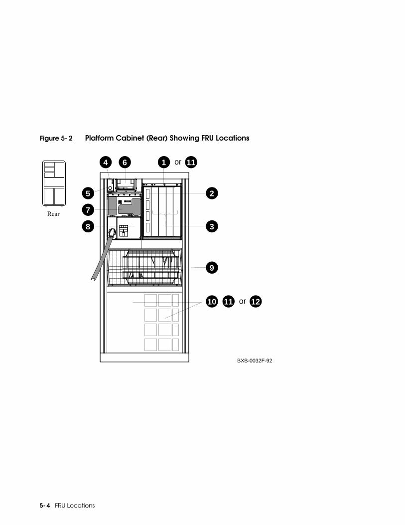
5-4 FRU Locations
Figure 5-2 Platform Cabinet (Rear) Showing FRU Locations
Rear
1 11or
10 11 12or
9
3
25
7
8
4 6
BXB-0032F-92
FRU Locations 5-5
1 70–28574–01 LSB centerplane and card cage 1, 2
2 E2044–AA IOP module3 E2043–AA or
E2043–BA orE2043–CA orE2046–AA
Memory module 64 Mbytes 3
Memory module 128 Mbytes 3
Memory module 256 Mbytes 3
Memory module 512 Mbytes 3
4 54–20300–01 Cabinet control logic module (CCL)
5 54–36203–04 CCL pressure sensor
6 TF85–AA Removable media device 1
Includes these FRUs:TK8554–19089–0154–20868–0117–03123–0117–03164–0117–03348–0117–03443–0117–03444–0117–03448–0117–03505–0117–03508–01
Disk driveDSSI controller moduleLocal disk converterLDC to CCL signalLDC to TF power +5/+12DSSI signal to bulkhead (TK85)Power LDC to bulkheadSignal LDC to bulkheadDSSI bus TF to bulkhead5V VTERM power48V power regulator to bulkhead
7 30–35143–01 DC distribution box
8 30–33798–01 or30–33798–02 or30–33798–03
AC input box
9 12–35173–01 Blower 1
10 DWLMA–AA/BA XMI plug-in unit 1 (see page 5-8)
11 BA654–AA Disk plug-in unit 3, 4 (see page 5-10)
12 H7237–AA Battery plug-in unit 1 (see page 5-12)
1 Removal and replacement of this FRU requires access to both the front and the rear of thecabinet.
2 This FRU is in the main cabinet only (cannot be located in the expander cabinet).3 This FRU can be located in either the front or the rear of the cabinet. 4 This FRU can be located in the top portion (front or rear) only in the expander cabinet.
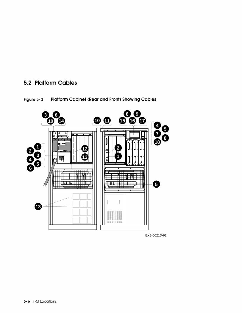
5-6 FRU Locations
5.2 Platform Cables
Figure 5-3 Platform Cabinet (Rear and Front) Showing Cables
13
13
6
3 6
12
10
4
12
5
BXB-0021D-92
5
8 915 16 17
45
7
1
18
3
2
10 1114
8

FRU Locations 5-7
1 17–03118–01 48V LSB power (gray)2 17–03118–02 48V LSB power (yellow)3 17–03119–01 48V power/signal to PIU
4 17–03127–01 AC to LDC
5 17–03126–01 48V power/sense to blower
6 17–03124–01 AC to CCL signal
7 17–03120–01 Control panel to CCL signal
8 17–03123–01 LDC to CCL signal
9 17–03164–01 +5/+12 LDC to tape power
10 17–03121–01 CCL to LSB bulkhead signal
11 17–03122–01 LSB bulkhead to LSB backplane
12 17–03085–01 I/O cable, long (to expander cabinet — 114 in)
13 17–03085–02 I/O cable, short (53 in)
14 17–03201–01 DEC power bus
15 17–03348–01 DSSI bulkhead signal
16 17–03443–01 LDC bulkhead power
17 17–03444–01 LDC bulkhead signal
18 17–03511–01 Control panel to CCL in expander cabinet

5-8 FRU Locations
5.3 FRUs in the XMI Plug-In Unit
Figure 5-4 XMI Plug-In Unit (Front) Showing FRU Locations
BXB-0343-92
12
3
4
8
7
6
5
9
10

FRU Locations 5-9
1 70–30396–01 XMI backplane assembly2 30–36010–01 Module A (power regulator)3 30–36009–01 Module B (power regulator)
4 T2028–AA DWLMA module (LSB to XMI — slot 8)
5 T2030–YA Clock and arbitration module (slot 7)These FRUs can reside in any1 XMI slot except 7 or 8:T2020–00 XMI to NI controllerT2027–00 XMI to FDDI controllerT2080–YA XMI to CI controllerT2036–AA XMI to DSSI controller
6 17–03162–01 Signal cable
7 17–03163–01 48V power cable
8 17–03202–01 Power distribution cable (rear of PIU)
9 17–03416–01 +5VB jumper (rear of PIU)
10 17–03533–01 Bulkhead to XMI signal (rear of PIU)
1 A module with an XMI corner must be in slot 1 or 14. For more information, see the VAX7000 Platform Service Manual.

5-10 FRU Locations
5.4 FRUs in the Disk Plug-In Unit
Figure 5-5 Disk Plug-In Unit (Front) Showing FRU Locations
9
5
1
2
3
4
6
7
8 10
115
1811
4
11
2
5 5
6
8
7
8
Underside of brick cover
BXB-0345-92

FRU Locations 5-11
1 through 3 , 5 through 8 , 10, and 11 are in each brick.
4 connects the bricks to each other.
9 runs up the center rear of the PIU.
1 RF73–EA RF73 disk drive
Includes these FRUs:
54–19119–0170–28814–01
RF73–EA ECM moduleRF73 HDA
2 54–20868–01 Local disk converter (LDC)3 54–21664–01 Disk control panel
4 17–02382–0x DSSI brick jumper cable (BC21Q-xx)
5 17–03417–01 RF73 signal
6 17–03418–01 LDC power
7 17–03419–01 LDC signal
8 17–03420–01 RF73 power
9 17–03422–01 Signal and power
10 17–03423–01 Disk control panel to bulkhead
11 17–03424–01 DSSI bus

5-12 FRU Locations
5.5 FRUs in the Battery Plug-In Unit
Figure 5-6 Battery Plug-In Unit (Rear) Showing FRU Locations
NOTE: The battery plug-in unit is shown in Figure 5-6 without its enclo-sure.
BXB-0344-92
1
2
3
4
8
7
6
5
1
1
3
5
3
(Block B)
(Block A)
(Block C)
42

FRU Locations 5-13
1 12–36168–02 Battery2 12–39982–01 Fuse (LPN–RK–90)3 17–03421–01 Battery sensor cable
4 17–03492–01 Intermediate cable, battery block A
5 17–03493–01 Intermediate cable, battery block B or C
6 17–03494–01 Power regulator A to battery block A
7 17–03494–02 Power regulator B to battery block B
8 17–03494–03 Power regulator C to battery block C


Controls and Indicators 6-1
Chapter 6
Controls and IndicatorsThis chapter describes controls and indicators on these system compo-nents:• Control Panel• TF85 Removable Media Device• Cabinet Control Logic Module• IOP Module• KA7AA Processor Module• Power Regulator• AC Input Box• BA651 XMI PIU Power Regulators• DWLMA Module• BA654 Disk PIU

6-2 Controls and Indicators
6.1 Control Panel
Figure 6-1 Control Panel
Table 6-1 Control Panel Indicator Lights
O
BXB-0015B-92
Front
Disable
Secure
Enable
Restart
Key On
Run
Fault
Light State Meaning
Key On On Power supplied to entire system; blower running.
(Green) Off Power supplied only to CCL module.
Run On Primary processor is running the operating sys-tem or user programs.
(Green) Off Primary processor is in console mode.
Fault On Fault on LSB, XMI, or an I/O bus.
(Yellow) Slow flash Power sequencing in progress or airflow error.
Fast flash Power system error, airflow error, or detectedtransition to keyswitch in Disable position.
Off The system passed self-test.

Controls and Indicators 6-3
6.2 TF85 Removable Media Device
Figure 6-2 TF85 Controls and Indicators
Table 6-2 TF85 Lights
BXB0017-92
WriteProtectedTape
inUse
UseCleaningTapeOperateHandle
ToLoad
Wait
Light
Openthis
Handle
Unload
TF85
Insert Tape
Closethis
Handle
ToUnload
Press Button
Wait
Light
Openthis
Handle
Remove
Tape
Front
Light Color State Meaning
Write Pro-tected
Orange OnOff
Tape write protectedTape write enabled
Tape inUse
Yellow SteadyBlinking
Drive readyDrive in use
Use Clean-ing Tape
Orange OnOff
Drive needs cleaningNo cleaning needed
OperateHandle
Green OnOffBlinking
OK to operate handleDo not operate handleDefective cartridge. Pull handleto the open position and removecartridge. Try another cartridge.
All fourlights
Blinking Drive fault. Reset by pressing theUnload button.

6-4 Controls and Indicators
6.3 Cabinet Control Logic Module
Figure 6-3 CCL Module LEDs
Table 6-3 CCL Module LEDs
BXB-0044D-92
Power LED
PIU 1
PIU 2
PIU 3
PIU 4
Rear
LED Meaning
Power LED Power is present on the CCL module.
PIU 1 – 4 Power is present in the PIU regulators in thequadrant indicated. (Q1 is to the left when view-ing the cabinet from the front, Q2 is behind Q1,Q3 is in the front right, and Q4 is behind Q3.)

Controls and Indicators 6-5
6.4 IOP Module
Figure 6-4 IOP (E2044-AA) Module LED
Table 6-4 IOP (E2044-AA) Module LED
Condition Meaning
On One of the following:• All IOP-specific and I/O adapter tests passed.• An I/O adapter test failed, and the error was isolated
to the adapter.
Off One of the following:• An IOP-specific test failed.• An I/O adapter test failed, and the error could not be
isolated to the adapter.• The processor module failed.

6-6 Controls and Indicators
6.5 KA7AA Processor Module
Figure 6-5 Processor (E2045) LEDs After Self-Test
Table 6-5 Processor (E2045) LEDs After Self-Test
Self-test failed
MSB
LSB
Failing test number
Self-test passed
STP
Test Result LEDs
Self-test passed —boot processor
STP LED and two LEDs above it are on.All others are off.
Self-test passed —secondary processor
STP LED and one LED above it are on.All others are off.
Self-test failed STP LED and two LEDs above it are off.Failing test number1 is in top seven LEDs:
1 – 55 SROM/self-test tests 1 – 55
56 – 65 CPU/memory interaction tests 1 – 10
66 – 72 Multiprocessor tests 1 – 7
1 The failing test number is in binary-coded decimal.

Controls and Indicators 6-7
Table 6-6 Self-Test LEDs Indicating Defective DC-to-DCConverter
Each module on the LSB has an on-board DC-to-DC converter. If the con-verter on one module is defective, the 2V reference voltage is disabled forall nodes, preventing any node from using the LSB. Table 6-6 indicateswhich module has the defective converter based on the state of the STPLEDs of all modules in the LSB.Use Table 6-6 when the Fault light on the control panel is on (see Section6.1) and the console prompt is displayed but the self-test map is not. Thisindicates that the LSB is good, but access to the bus is not possible.
ProcessorModules
Memory Modules IOP Module
Defective Con-verter on ThisModule
One module’sSTP LED is off;all others areon.
All STP LEDsare on.
STP LED is off. Processor mod-ule with STPLED off
All STP LEDsare on.
One module’sSTP LED is off;all others areon.
STP LED is off. Memory modulewith STP LEDoff
All STP LEDsare on.
All STP LEDsare on.
STP LED is off. IOP module
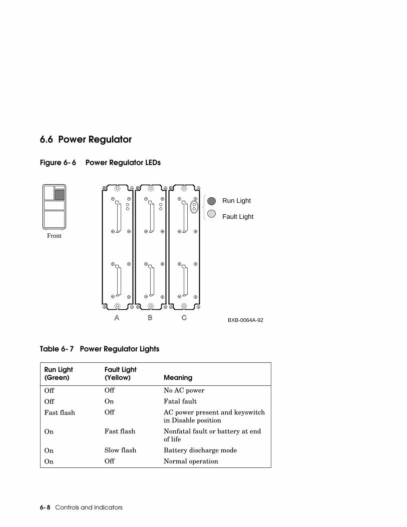
6-8 Controls and Indicators
6.6 Power Regulator
Figure 6-6 Power Regulator LEDs
Table 6-7 Power Regulator Lights
Front
Run Light Fault Light
BXB-0064A-92
Run Light(Green)
Fault Light(Yellow) Meaning
Off Off No AC power
Off On Fatal fault
Fast flash Off AC power present and keyswitchin Disable position
On Fast flash Nonfatal fault or battery at endof life
On Slow flash Battery discharge mode
On Off Normal operation

Controls and Indicators 6-9
6.7 AC Input Box
Figure 6-7 AC Input Box — Indicators on Circuit Breaker
Table 6-8 AC Input Box — Indicators on Circuit Breaker
NOTE: In the Japanese version (30–33798–03), all poles trip if one does,causing all indicators to turn green.
BXB-0049A-92
Rear
C B A S
Breaker Indicator
A - Regulator slot A B - Regulator slot B C - Regulator slot C S - Sensor circuit
Color Meaning
Red Pole is in on position; not tripped.
Green Pole is in off position or tripped due to an overload.

6-10 Controls and Indicators
6.8 BA651 XMI PIU Power Regulators
Figure 6-8 XMI PIU Power Regulators
Front
BXB-0074C-92
INPUT VOLTAGE 48 VDC
INPUT CURRENT 5A MAX
d i g i t a l
INPUT VOLTAGE 48 VDC
INPUT CURRENT 28A MAX
MOD OK OC OT OV 48V
RESET
V-OUT
DISABLE
MOD OK OC OT OV 48V
MOD OK OC OT OV 48V
RESET
V-OUT
DISABLE
MOD OK OC OT OV 48V
Regulator B Regulator A

Controls and Indicators 6-11
Table 6-9 XMI PIU Power Regulator Lights (Regulators A and B)
Table 6-10 XMI PIU Power Switches (Regulator B)
Light Color State MeaningDoes lightlatch?
MOD OK Green On Regulator is working. No
Off Regulator is not working.
OC Yellow On Overcurrent condition Yes
OT Yellow On Overtemperature condi-tion
Yes
OV Yellow On Overvoltage condition Yes
48V Green On 48V is present. No
Switch Function
Reset Momentary switch resets all lights on regulatorsA and B.
Enable/Disable When this switch is in the Disable position, theoutput of both PIU power supplies is inhibited.

6-12 Controls and Indicators
6.9 DWLMA Module
Figure 6-9 DWLMA (T2028-AA) Module LEDs
Table 6-11 DWLMA (T2028-AA) Module LEDs
ES
FTLERR
POK
DBGDIS
STP
LED Color Desired Condition
STP — Self-Test Passed Yellow On
DBGDIS — Debug Disable Green On
POK — Power OK Green On
FTLERR — Fatal Error Red Off
ES — Error Summary Red Off

Controls and Indicators 6-13
6.10 BA654 Disk PIU
Figure 6-10 Disk Brick Control Panel
Table 6-12 Disk Brick Controls and Indicators
BXB-0045A-92
Power Ready Write Protect Fault
Ready Write Protect Fault Power
ControlPushbuttonPosition Light Function
Power(Green)
InOut
OnOff
DC power presentDC power not present
Ready(Green)
InOut
OnOff
ISE is on-lineISE is off-line
Wrt Prot(Yellow)
InOut
OnOff
Write-protect enabledWrite-protect disabled
Fault(Red)
Momentaryswitch
OnOffSlow flashFast flash
Fault conditionNormal operationISE calibrations in progressDisk control panel failure


Restoring Corrupted ROMs 7-1
Chapter 7
Restoring Corrupted ROMsThe following list tells you how to determine when to use these sections ofthis chapter: • Restoring a Corrupted EEPROM
Use this section when the message "EEPROM image failed to verify" isdisplayed on the console terminal.
• Restoring Corrupted Firmware on an AdapterUse this section when an adapter fails self-test and the problem is cor-rupted firmware.
• Restoring Corrupted Firmware on a CPUUse this section when you power up the system and the promptVAX-7000/10000-FRRC> is displayed on the console terminal.

7-2 Restoring Corrupted ROMs
7.1 Restoring a Corrupted EEPROM
Example 7-1 Using the Build EEPROM Command to Restore aCorrupted EEPROM
EEPROM image failed to verifyEEPROM environment parameters not set upFail to update EEPROM envar on CPU 1
>>> build eepromCreating new EEPROM imageSystem Serial Number> gao1234567Module Serial Number> sgo0000001Module Unified 2-5-2-4 Part Number> 80-E2045-AA-0E04Module Firmware Revision> 1.00
>>> initialize
NOTE: See Chapter 3 for more information on the console commands forthe EEPROM.
For more information:
VAX 7000 System Service ManualVAX 7000 Console Reference Manual

Restoring Corrupted ROMs 7-3
7.2 Restoring Corrupted Firmware on an Adapter
If an adapter fails self-test, use this procedure to determine if the firmwareis corrupted, and if it is, to update the firmware:1. Boot the console CD-ROM (Example 7-2).2. Use the LFU display or show command to indicate (by returning the
mnemonic "unknown") if firmware has been corrupted (Example 7-3).3. Use the LFU update command to write the new firmware (Example
7-4).4. Exit (Example 7-5).
Example 7-2 Booting LFU
>>> boot exa0 -file ISL_LVAX_V01resulting file is mopdl:ISL_LVAX_V01/exa0 ...... Load complete! [boot information]Network Initial System Load FunctionVersion 1.1FUNCTION FUNCTIONID1 - Display Menu2 - Help3 - Choose Service4 - Select Options5 - StopEnter a function ID value: 3OPTION OPTIONID1 - Find Services2 - Enter known Service NameEnter an Option ID value: 1
WorkingServers found: 3Service Name Format:Service NumberService NameServer NameEthernet ID#1INFO4$RZ57INFO408-00-2B-26-A6-98#26000_DIAG_H

7-4 Restoring Corrupted ROMs
Example 7-2 Booting LFU (Continued)
INFO308-00-2B-16-04-D4#3VAX7000_V01OPUS_ESS08-00-2B-18-A9-75Enter a Service Number or <CR> for more: 3
Copyright Digital Equipment Corporation1992
All Rights Reserved.Loadable Environment Rev: V1.0-1625 Jul 12 1992 10:50:56
***** Loadable Firmware Update Utility *****Version 2.01 16-jun-1992
---------------------------------------------------------------- Function Description----------------------------------------------------------------
Display Displays the system’s configuration table. Exit Return to loadable offline operating environment. List Lists the device types and firmware revisions supported by this revision of LFU. Modify Modifies port parameters and device attributes. Show Displays device mnemonic, hardware and firmware revisions. Update Replaces current firmware with loadable data image. Verify Compares loadable and device images. ? or Help Scrolls the function table.----------------------------------------------------------------Function?

Restoring Corrupted ROMs 7-5
Example 7-3 LFU Display and Show Commands
Function? disp Name Type Rev Mnemonic FW Rev HW Rev LSB0+ KA7AA (8002) 0000 ka7aa0 1.00 E04 7+ MS7AA (4000) 0000 ms7aa1 N/A A01 8+ IOP (2000) 0001 iop0 N/A A
C0 XMI xmi08+ DWLMA (102A) A5A6 dwlma0 N/A A C+ KDM70 (0C22) 1E11 kdm700 3.00 E+ DEMNA (0C03) 060B demna0 6.08
C1 XMI xmi11+ ????? (0000) 0000 unknown0 8+ DWLMA (102A) A5A6 dwlma1 N/A A A+ CIXCD (0C05) EB11 cixcd0 69.00 A01
Function? sho *
Firmware Hardware Revision Revision
ka7aa0 + 1.00 E04ms7aa0 -- -- not supported.iop0 -- -- not supported.xmi0 -- -- not supported.kdm700 3.00 Cannot be readdemna0 -- -- not supported.unknown0 -- -- Updates only.cixcd0 + 69.00 A01
’+’ indicates the update firmware revision is greater than the adapter’s firmware revision.
Function?

7-6 Restoring Corrupted ROMs
Example 7-4 LFU Update Command
Function? update unknown0Enter device name or ’exit’ to skip this device.Device name? cixcdHardware revision? A01WARNING: updates may take several minutes to complete for each device
DO NOT ABORT!unknown0 Updating to 70.00... Reading Device... Verifying 70.00...PASSED.
Function?
Example 7-5 LFU Exit Command
Function? exit
Initializing...
F E D C B A 9 8 7 6 5 4 3 2 1 0 NODE # A M . . . . . P P TYP o + . . . . . + + ST1 . . . . . . . E B BPD o + . . . . . + + ST2 . . . . . . . E B BPD + + . . . . . + + ST3 . . . . . . . E B BPD
. . . . + . + . + . . . + . C0 XMI + . . . . . . . . . . . . . . C1 . . . . . . . . . . . . . . C2 . . . . . . . . . . . . . . C3
. A0 . . . . . . . ILV .128 . . . . . . . 128MbFirmware Rev = V1.0-1625 SROM Rev = V1.0-0 SYS SN = GAO1234567 >>>
For more information:
VAX 7000 System Service ManualVAX 7000 Operations Manual

Restoring Corrupted ROMs 7-7
7.3 Restoring Corrupted Firmware on a CPU
Use this procedure when the prompt VAX-7000/10000-FRRC> appears atthe console terminal after power-up. (This prompt appears only if the con-sole terminal is set at 9600 baud.) This prompt indicates that the firmwarein the FEPROMs on the processor module has been corrupted. The following must be available for you to use this procedure:• A source system that can logically connect, through the console port, to
the system that has the corrupted firmware.— The source system can be on site or remote.— The source system must have access to an InfoServer.— The program Kermit must reside on the source system.
• The VAX 7000 console CD-ROM with the fileVAX7000_10000_CONSOLE_IMAGE.GROM.
Do the following to restore the corrupted firmware. All work is done at thesource system, and the procedure takes approximately 10 minutes.1. Set up the source system (Example 7-6):
a. Set the speed of the terminal at which you are working to 9600baud.
b. Bind the CD-ROM volume name to a virtual disk container.c. Mount the InfoServer.
2. Make a physical connection from the source system to the system withthe corrupted firmware. For example, use an RS232 cable to connectfrom a DMB32 on the source system to the console port on the systemwith the corrupted firmware.
3. Run Kermit (Example 7-7) and set the parameters as shown in the re-sponse to the show all command in the example.
4. Connect to the system with the corrupted firmware and downline loadthe correct code (Example 7-8).
7-8 Restoring Corrupted ROMs
Example 7-6 Preparing the Source System to Restore CorruptedFirmware on a CPU
$ set term/speed=9600/perm txa3:$ mcr ess$ladcpLADCP> bind VAX7000_V01VAX7000_V01 is bound to DAD104LADCP> exit$ mount/ov=id dad104$ dir dad104:[sys0.sysexe]
Directory DAD104:[SYS0.SYSEXE]
VAX7000_1000_CONSOLE_IMAGE.GROM
Example 7-7 Running Kermit and Setting Parameters
$ kermitKermit-32> set file type binaryKermit-32> set retry packet 5Kermit-32> set send time 5Kermit-32> show allVMS Kermit-32 version 3.3.111
Block check type One character checksum Debugging OFF Delay 5 (sec) Server sends NAKs every 75 seconds while waiting for acommand Escape character 035 (octal) File type BINARY File naming Normal form Handshaking character None Incomplete file disposition Discard Line used (Optional) Local echo OFF Parity type None
Retry maximums
Initial connection 5 (dec) Sending a packet 5 (dec)
Send parameters
Packet length 80 (dec) Padding length 0 (dec)

Restoring Corrupted ROMs 7-9
Example 7-7 Running Kermit and Setting Parameters (Cont)
Padding character 000 (octal) Time out 5 (sec) End of line character 015 (octal) Quoting character 043 (octal) Start of packet 001 (octal)
Receive parameters
Packet length 80 (dec) Padding length 0 (dec) Padding character 000 (octal) Time out 5 (sec) End of line character 015 (octal) Quoting character 043 (octal) 8-bit quoting character 046 (octal) Start of packet 001 (octal)
Transmit parameters
Delay 0.0 (sec) Echo OFF Repeat quoting character 176 (octal)
Example 7-8 Downline Loading Code to Corrupted FEPROMs
Kermit-32> connect txa5:VAX-7000/10000-FRRC> r !Prepare system to receiveVAX-7000/10000-FRRC> Ctrl/] C !Return to KermitKermit-32> send vax7000_10000_console_image.grom
!Transmit codeKermit-32> connect !Reconnect to target systemVAX-7000/10000-FRRC> c !Verify checksum of imageVAX-7000/10000-FRRC> p !Copy program image to
!FEPROMsVAX-7000/10000-FRRC> i !Reset nodeVAX-7000/10000-FRRC> Ctrl/] C !Return to KermitKermit-32> exit !Return to DCL$
For more information:
VAX 7000 System Service Manual


System Errors 8-1
Chapter 8
System ErrorsThis chapter includes information on the machine check frame and theparse trees. Sections include:• Machine Check Frame• Machine Check Parse Tree• Hard Error Parse Tree• Soft Error Parse Tree• I/O Port Parse Tree• DWLMA Parse Tree

8-2 System Errors
8.1 Machine Check Frame
Figure 8-1 Machine Check Frame
31 29 28 23 15 9 08 7
Parameter Byte Count (18 Hex)
BXB-0196-92
AST x MCHK Code X CPU_ID
INT SYS Register
SAVEPC Register
VA Register
Q Register
Rn Mod Opcode VR
PC
PSL
1626 25
x x
:SP
:SP + 4
:SP + 8
:SP + 12
:SP + 16
:SP + 20
:SP + 24
:SP + 28
:SP + 32
For more information:
KA7AA CPU Technical ManualVAX 7000 Advanced Troubleshooting

System Errors 8-3
Table 8-1 Machine Check Frame Parameters
Longword Bits Contents
SP+0 <31:0> Byte count. The size of the stack frame in bytes,not including the PC, PSL, or the byte count long-word. Stack frame PC and PSL values should al-ways be referenced using this count as an offsetfrom the stack pointer.
SP+4 <31:29> AST LVL. The current value of the register.
<23:16> Machine check code. The reason for the machinecheck, as listed in Table 8-2.
<7:0> CPUID. Contains the current value of the CPUIDregister.
SP+8 <31:0> INT.SYS register. The value of the INT.SYS regis-ter, which is read onto the A-bus by the microcode.
SP+12 <31:0> SAVEPC register. The SAVEPC register, which isloaded by microcode with the PC value in certaincircumstances. It is used in error handling for PTEread errors with PSL <FPD> set in this stackframe.
SP+16 <31:0> VA register. The contents of the Ebox VA register,which may be loaded from the output of the ALU.
SP+20 <31:0> Q register. The contents of the Ebox Q register,which may be loaded from the output of the shifter.
SP+24 <31:28> Rn. The value of the Rn register, which is used toobtain the register number for the CVTPL andEDIV instructions. In general, the value of thisfield is unpredictable.
<25:24> Mod. A copy of the currrent mode field, PSL<CUR_MOD>.
<23:16> Opcode. Bits <7:0> of the instruction opcode. TheFD bit is not included.
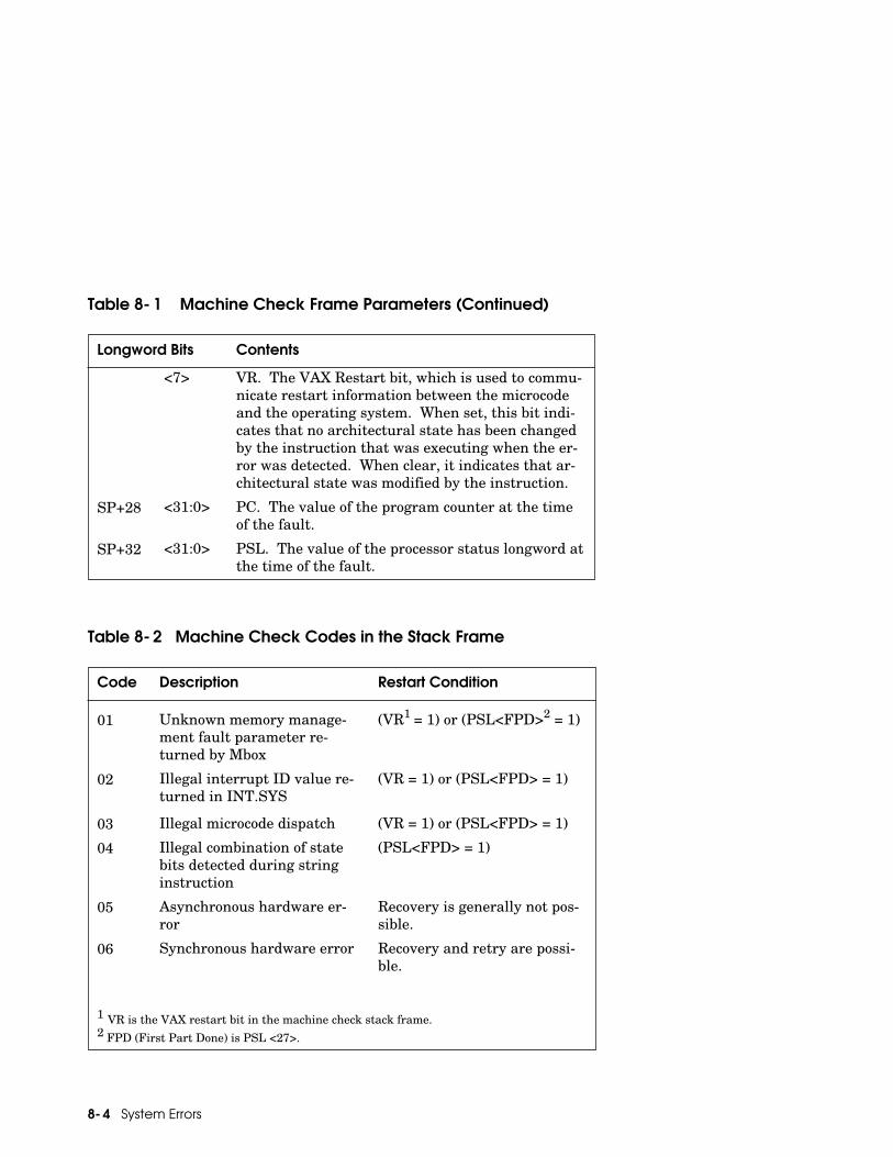
8-4 System Errors
Table 8-1 Machine Check Frame Parameters (Continued)
Table 8-2 Machine Check Codes in the Stack Frame
Longword Bits Contents
<7> VR. The VAX Restart bit, which is used to commu-nicate restart information between the microcodeand the operating system. When set, this bit indi-cates that no architectural state has been changedby the instruction that was executing when the er-ror was detected. When clear, it indicates that ar-chitectural state was modified by the instruction.
SP+28 <31:0> PC. The value of the program counter at the timeof the fault.
SP+32 <31:0> PSL. The value of the processor status longword atthe time of the fault.
Code Description Restart Condition
01 Unknown memory manage-ment fault parameter re-turned by Mbox
(VR1 = 1) or (PSL<FPD>2 = 1)
02 Illegal interrupt ID value re-turned in INT.SYS
(VR = 1) or (PSL<FPD> = 1)
03 Illegal microcode dispatch (VR = 1) or (PSL<FPD> = 1)
04 Illegal combination of statebits detected during stringinstruction
(PSL<FPD> = 1)
05 Asynchronous hardware er-ror
Recovery is generally not pos-sible.
06 Synchronous hardware error Recovery and retry are possi-ble.
1 VR is the VAX restart bit in the machine check stack frame.2 FPD (First Part Done) is PSL <27>.

System Errors 8-5
8.2 Machine Check Parse Tree
Figure 8-2 Machine Check Parse Tree
MCHK_UNKNOWN_MSTATUS
MCHK_INT.ID_VALUE
MCHK_CANT_GET_HERE
MCHK_MOVC.STATUS
MCHK_ASYNC_ERROR
1 2 3
Unknown memory management status error
TBSTS.LOCK <0>TBSTS.DPERR <1>
TBSTS.DPERR <2>
None of the above
ECR.S3_STALL_TIMEOUT
None of the above
MCHK_SYNC_ERROR
ICSR.LOCK <2>ICSR.DPERR <3>
not PCSRS.PTE_ER <10>
ICSR.TPERR <4>
Otherwise...
BIU_STATE.FILL_ECC <8> and not BIU_STAT.FILL_CRD <9>
BIU_STAT.FILL_DSP_CMD <19:16> = DREAD
Otherwise...
BIU_STAT.FILL_DSP_CMD <19:16> = IREAD
Illegal interrupt ID error
Impossible microcode address
MOVCx status encoding error
TB PTE data parity error
TB tag parity error
Inconsistent error
S3 stall timeout
Inconsistent error
Select ALL, at least one.
Select ALL
VIC data parity error
VIC tag parity error
Inconsistent error
Select ONE
Select ONE
A
B
Inconsistent error
EXE$MCHK
BXB-0301-92
Code (Hex)
01
02
03
04
05
06
Select ONE
Select ALL

8-6 System Errors
Figure 8-2 Machine Check Parse Tree (Continued)
1 2 3
BIU_STAT.FILL_SEO <14>
BIU_STAT.BIU_SEO <7>
BIU_STAT.BC_TPERR <2>
None of the above
PCSTS.PTE_ER <10>BIU_STAT.FILL_ECC <8>
not BIU_STAT.CRD <9>
Lost B-cache ECC error
Lost B-cache fill error
Select ONE
Inconsistent error
Select ONE
BXB-0302-92
1 2 3
BIU_STAT/BIU_DSP_CMD <6:4> = DREADD-stream read B-tag parity error
BIU_STAT/BIU_DSP_CMD <6:4> = IREADI-stream read B-tag parity error
BIU_STAT.BC_TCPERR <3> Select ONE
BIU_STAT/BIU_DSP_CMD <6:4> = DREADD-stream read B-tag parity error
BIU_STAT/BIU_DSP_CMD <6:4> = IREADI-stream read B-tag parity error
BIU_STAT.BIU_HERR <0> E
Select ONE
BIU_STAT.FILL_DSP_CMD<19:16> = DREADC
BIU_STAT.FILL_DSP_CMD<19:16> = IREADD
BIU_STAT.FILL_SEC <14> Lost ECC errors during PTE read
BIU_STAT.BC_TPERR <2> Select ONE
BIU_STAT.BIU_DSP_CMD<6:4>
= DREAD
BIU_STATE.BIU_DSP_CMD<6:4>
= IREAD
Otherwise...
PTE D-stream read B-tag parity error
PTE I-stream read B-tag parity error
PTE write B-tag parity error
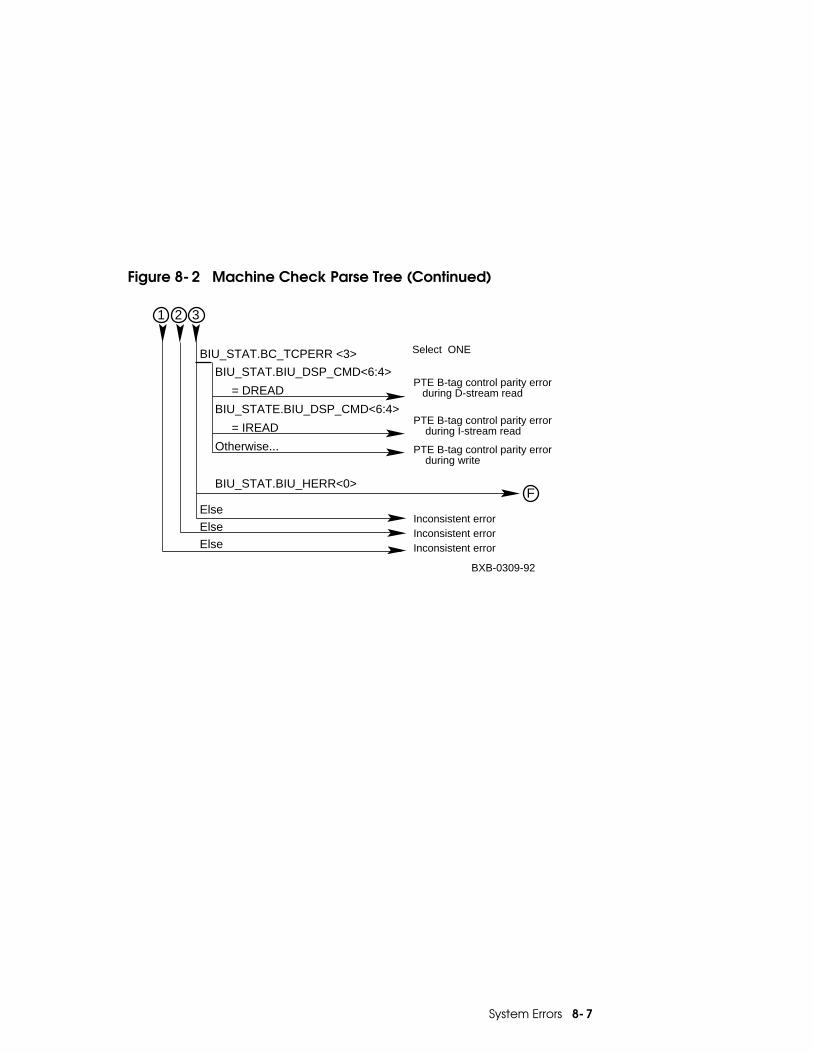
System Errors 8-7
Figure 8-2 Machine Check Parse Tree (Continued)
BXB-0309-92
1 2 3
BIU_STAT.BC_TCPERR <3> Select ONE
BIU_STAT.BIU_DSP_CMD<6:4>
= DREAD
BIU_STATE.BIU_DSP_CMD<6:4>
= IREAD
Otherwise...
BIU_STAT.BIU_HERR<0>
PTE B-tag control parity error during D-stream read
PTE B-tag control parity error during I-stream read
PTE B-tag control parity error during write
F
Inconsistent error Inconsistent error Inconsistent error
Else Else Else

8-8 System Errors
Figure 8-2 Machine Check Parse Tree (Continued)
LBER.UCE <1>
MERA.UCER
Other CPU LMERR.BDATA_DBE
Else
ABC_TAG <11>
D-stream cache double-bit error
D-stream read double-bit error
D-stream error on other CPU
D-stream read LSB double-bit error
LBER.UCE <1>
MERA.UCER
Other CPU LMERR.BDATA_DBE
Else
BBC_TAG <11>
I-stream cache double-bit error
I-stream read double-bit error
I-stream error on other CPU
I-stream read LSB double-bit error
LBER.UCE <1>
MERA.UCER
Other CPU LMERR.BDATA_DBE
Else
CBC_TAG <11>
PTE D-stream cache double-bit error
PTE D-stream read double-bit error
PTE D-stream error on other CPU
PTE D-stream read LSB double-bit error
LBER.UCE <1>
MERA.UCER
Other CPU LMERR.BDATA_DBE
Else
�DBC_TAG <11>
PTE I-stream cache double-bit error
PTE I-stream read double-bit error
PTE I-stream error on other CPU
PTE I-stream read LSB double-bit error BXB-0310-92

System Errors 8-9
Figure 8-2 Machine Check Parse Tree (Continued)
1 2
BIU_STAT.BIU_DSP_CMD<6:4> = Read
Read ARB drop
Inconsistent error
LBER.NSES<18>
IMERR.ARBDROP<12>
Else
LBECR.CA<37:35> = CSR Read
LBER.CA<37:35> = Read
LBER.CA<37:35> = Private
E
LBER.E<0> and LBERCR1.CID<10:7> = This_CPU LBER.NXAE<12>
LSB command parity error
Previous system error latched
Inconsistent
LBER.E
Else
Inconsistent
NXM to LSB memory
NXM to self I/O space
NXM to LSB I/O space
BXB-0312-92
LBER.CPE<5>
Else
BIU.STAT.BIU_DSP_CMD<6:4>=Loadlock
Read ARB drop
LEVI B-cache tag parity error (lookup)
LBER.NSES<18>IMERR.ARBDROP<10>
IMERR.BTAGPE<5>
IMERR.BSTATPE<4>
ElseInconsistent
LEVI B-cache status parity error (lookup)

8-10 System Errors
Figure 8-2 Machine Check Parse Tree (Continued)
Memory data
1
LBER.E<0> and LBECR.CA<37:35> = Read and LBECR1.CID<10:7> = This_CPU
LBER.NXAE<12>
LBER.CPE<5>
Else
LBER.3
Else
Else
Write LSB NXM
LSB command parity error
Previous system error latched
Inconsistent
InconsistentBXB-0313-92
E Continued
Inconsistent
2

System Errors 8-11
Figure 8-2 Machine Check Parse Tree (Continued)
BIU_STAT.BIU_DSP_CMD<6:4>=Read
LBER.NSES<18>
IMERR.ARBDROP<12>
ElsePTE read ARB drop
Inconsistent error
F
LBER.E<0> and LBECR1.CID<10:7> = This_CPU
LBER.NXAE<12>
LBER.CPE<5>
Else
PTE NXM to LSB memory
PTE LSB command parity error
Previous system error latched
Inconsistent
LBER.E
Else
BXB-0314-92
Inconsistent
BIU_STAT.BIU_DSP_CMB<6:4>=Loadlock
PTE read ARB drop
PTE LEVI B-cache tag parity error (lookup)PTE LEVI B-cache status parity error (lookup)
IMERR.ARBDROP<10>
IMERR.BTAGPE<5>
IMERR.BSTATPE<4>
ElseInconsistent
LBER.E<0> and LBECR.CA<37:35> = Read and LBECR1.CID<10:7> = This_CPU (Memory data)
PTE write LSB NXM
PTE LSB command parity error
LBER.EPrevious system error latched
ElseInconsistent
Inconsistent
LBER.NXAE<12>
LBER.CPE<5>
Else

8-12 System Errors
8.3 Hard Error Parse Tree
Figure 8-3 Hard Error Parse Tree
BIU_STAT.LOST_WRITE_ERR
Select ALL, at least one...
B-cache tag parity error on a write from MBOX
BXB-0318-92
EXE$HERR
BIU_STAT.BC_TPERR and BIU_STAT.BIU_DSP_CMD<6:4> = WRITE
BIU_STAT.BC_TCPERR and BIU_STAT.BIU_DSP_CMD<6:4> = WRITE
B-cache tag control parity error on a write from MBOX
BIU_STAT.FILL_ECC and not BIU_STAT.CRD and BIU_STAT.BIU_DSP_CMD<6:4> = WRITE
Uncorrectable ECC error on a write from MBOX
BIU_STAT.BIU_HERR and BIU_STAT.BIU_DSP_CMD<6:4> = WRITE
LBER.E or LBER.NSES
A
B
Inconsistent error
Uncorrectable ECC error on a write from MBOX
Else

System Errors 8-13
Figure 8-3 Hard Error Parse Tree (Continued)
1 2
BIU_STAT.BIU_DSP_CMD<6:4>=Write
(getting memory data for write)LBER.NSES<18> and LBECR.CA<37:35> = Read and LBERC1.CID = This_CPU
IMERR.ARBDROP<10>
ElseRead ARB drop
Inconsistent error
A
BXB-0319-92
(B-cache contains shared data)LBER.NSES<18> and LBERCR.CA<37:35> = Write and LBECR1.CID<10:7> = This_CPU
IMERR.ARBDROP<10>
ElseWrite ARB drop
Inconsistent error
(LSB problem getting data)
LBER.E<0> and LBECR.CA<37:35> = Read and LBECR1.CID<10:7> = This_CPU
LBER.NXAE<12>
LBER.CPE<5>
Else
Read LSB NXM
LSB read command parity error
Inconsistent error
(B-cache contains shared data)LBER.E<0> and LBECR.CA<37:35>=Write and LBECR1.CID<10:7>=This CPU
LBER.NXAE<12>
LBER<CPE<5>
Else
Write LSB NXM
LSB command parity error
InconsistentLBER.E<0> and LBECR.CA=CSR Write and LBECR1<10:7>=This CPU
(I/O Cycle)
LBER.CDPE
LBER.NXAE<12>
Else
Write CSR data parity error
Write CSR NXM
Inconsistent

8-14 System Errors
Figure 8-3 Hard Error Parse Tree (Continued)
BXB-0320-92
1 2 A Continued
Previous system error latched
Inconsistent
LBER.O
Else
BIU_STAT.BIU_DSP_CMD<6:4>=Write Unlock
LBER.NSES<18>
IMERR.ARBDROP<10>
IMERR.BTAGPE<5>
IMMER.BSTATPE<4>
Else
Read ARB drop
LEVI B-cache tag parity error (lookup)LEVI B-cache status parity error (lookup)Inconsistent
Inconsistent
InconsistentElse
Else

System Errors 8-15
Figure 8-3 Hard Error Parse Tree (Continued)
LBER.NSESSelect ALL, at least one...
Serious LEVI failure
B-cache tag parity error
LMERR.PMAPPE<3:0>
LMERR.BTAGPE
LMERR.BDATASBE
LMERR.BDATADBE
LMERR.BMAPPE
LMERR.BSTATPE
None of the above...
B
BXB-0322-92
LMERR.ARBDROP or LMERR.ARBCOL
C
D
E
F
P-cache backmap parity error
LBER.ESelect ALL, at least one...
LSB cache protocol error
LBER.SHE or LBER.DIE
LSB synchronization failure
LBER.STE or LBER.CNFE or LBER.CAE
LBER.TDE
LBER.CTCESelect ONE...
Inconsistent
Control transmit check errors
Select ONE...Correctable datacheck error on LSB writeUncorrectable datacheck error on LSB writeLSB write CSR data parity error
Inconsistent error
LBER.CE
LBER.UCE
LBER.CDPE
None of the above...
LBER.DTCE
LBER.CE
LBER.UCE
None of the above...
Correctable ECC error on LSB
Inconsistent error
Uncorrectable ECC error on LSB
1 2

8-16 System Errors
Figure 8-3 Hard Error Parse Tree (Continued)
1 2
1
BXB-0323-92
B Continued2
Lost LSB command parity error
Lost LSB CSR data parity error
Lost LSB correctable ECC error
Lost LSB uncorrectable ECC error
LBER.CPE2
LBER.CDPE2
LBER.CE2
LBER.UCE2
LBER.UCE and not LBER.TDE
LBECR1.CA<37:35>=READLBECR1.CID=THIS_LNP
Otherwise...
Correctable ECC error on LSB read fill
Bystander - correctable ECC error on LSB read
Otherwise...LBECR1.SHARED Otherwise...
Correctable ECC error during B-cache update
Bystander - correctable ECC error on LSB write
Bystander - LSB read CSR data parity errorLSB ERR asserted by other node(s)
Inconsistent error
LBER.CDPE
Any Adapter - LBER.E Set
None of the Above...
LBER.UCE and not LBER.TDELBECR1.CA<37:35>=Read
LBECR1.CID=This_CPU
Otherwise...
Uncorrectable ECC error on LSB read fillBystander - uncorrectable ECC error on LSB readOtherwise...
LBECR1.SHARED
Otherwise...Bystander - uncorrectable ECC error on LSB write
Uncorrectable ECC during B-cache update

System Errors 8-17
Figure 8-3 Hard Error Parse Tree (Continued)
1 2
1
BXB-0324-92
B Continued
LBER.E<0> and LBECR1.CID=IOP_node (IOP is cmdr)
IOP_LBER.STE<10>
IOP_LBER.CAE<13>
IOP_LBER.CNFE<11>
IOP_LBECR1.CA<37:35>=Write
Else
IOP_LBER.NXAE<12>
IOP_LBER.CPE<5>
IOP_LBER.CE<3>
IOP_LBER.UCE<1>
Inconsistent
Else
IOP_LBER.NXAE<12>
IOP_LBER.CPE<5>
IOP_LBER.CE<3>
IOP_LBER.UCE<1>
Inconsistent
IOP_LBERCR1.CA<37:35> = Read
Else
IOP_LBER.NXAE<12>
IOP_LBER.CPE<5>
IOP.LBER.CE<3>
IOP_LBER.UCE<1>
Inconsistent
IOP_LBECR1.CA<37:35> = Wrt CSR

8-18 System Errors
Figure 8-3 Hard Error Parse Tree (Continued)
1
BXB-0325-92
B Continued2
IOP_LBER.CPE2<6>
IOP_LBER.CDPE2<8>
IOP_LBER.CE2<4>
Else
IOP_LBER.UCE2<2>
IOP_LBER.NESES<18>
Inconsistent
Inconsistent

System Errors 8-19
Figure 8-3 Hard Error Parse Tree (Continued)
LEVI read of B-cache correctable error from LSB request (dirty block)
LEVI LSB write correctable error
Inconsistent
LBECR1.CA<37:35> = Read and LBECR1.CID = not this node
C
BXB-0326-92
Else
LBECR1.CA<37:35> = Write and LBECR1.CID<10:7> = This node
LEVI read of B-cache uncorrectable error from LSB request (dirty block)
LEVI LSB write uncorrectable error
Inconsistent
LBECR1.CA<37:35> = Read and LBECR1.CID = not this node
D
Else
LBECR1.CA<37:35> = Write and LBECR1.CID <10:7> = This node
LEVI lookup B-cache B-map parity error from LSB read request
LEVI lookup B-cache B-map parity error from write request
LEVI lookup B-cache B-map parity error from write
LBECR1.CA<37:35> = Read and LBECR1.CID = not this node
E
Else
LBECR1.CA<37:35> = Write and LBECR1.CID<10:7> = not this node
LEVI lookup B-cache STS parity error from LSB read request
LEVI lookup B-cache STS parity error from LSB write request
LEVI lookup B-cache STS parity error from LSB write
LBECR1.CA<37:35> = Read and LBECR1.CID = not this node
F
Else
LBECR1.CA<37:35> = Write and LBECR1.CID<10:7> = not this node

8-20 System Errors
8.4 Soft Error Parse Tree
Figure 8-4 Soft Error Parse Tree
ICR.LOCK
VIC data parity error - bank 0
VIC tag parity error - bank 0
VIC data parity error - bank 1
VIC tag parity error - bank 1
ICSR.DPERR0
ICSR.TPERR0
ICSR.DPERR1
ICSR.TPERR1
None of the above...
BXB-0329 -92
EXE$SERR
Inconsistent errorPCSTS.LOCK
Select ALL, at least one...
P-cache data parity error
P-cache tag parity error in right bank
P-cache tag parity error in left bank
Inconsistent error
PCSTS.DPERR
PCSTS.RIGHT_BANK
PCSTS.LEFT_BANK
Otherwise...
not PCSTS.PTE_ER_WRSelect ALL, at least one...
Read timeout
Tag parity error on read
Tag control parity error on read
Correctable ECC error on fill or write merge
BIU_STAT.BIU_HERR and BIU_STAT.BIU_CMD = READ
Uncorrectable ECC error on fill
BIU_STAT.LOST_WRITE_ERRWrite error after SERR
PCSTS.PTE_ER_WRHard error on a PTE DREAD for write or write unlock
BIU_STAT.BIU_TPERR and BIU_STAT.BIU_CMD = READ
BIU_STAT.BIU_TCERR and BIU_STAT.BIU_CMD = READ
BIU.STAT.FILL_ECC and BIU_STAT.CRD
BIU_STAT.FILL_CERR and not BIU_STAT.CRD and BIU_STAT.ARB_CMD = READ
BIU_STAT.BIU_SERR
None of the above...System soft error interrupt (not used)
Inconsistent error
None of the above...Inconsistent error
Select ALL, at least one...

System Errors 8-21
8.5 I/O Port Parse Tree
Figure 8-5 IOP Parse Tree
1
IOP_LBER.NES<18>
Multiple interrupt error
Down vortex error
Up vortex error
IPC internal error
IPCNSE.MULT_INTR_ERR<20>
IPCNSE.DN VRTX ERR<19>
IPCNSE.UP VRTX ERR<18>
IPCNSE.IPC IE<17>
IPCNSE.UP_HIC_IE<16>
BXB-0316-92
UP HIC internal error
Up channel 3 parity error
Up channel 2 parity error
Up channel 1 parity error
Up channel 0 parity error
IPCNSE.UP_CHAN_PAR_ERROR_3<15>
IPCNSE.UP_CHAN_PAR_ERROR_2<14>
IPCNSE.UP_CHAN_PAR_ERROR_1<13>
IPCNSE.UP_CHAN_PAR_ERROR_0<12>
Up channel 3 packet error
Up channel 2 packet error
Up channel 1 packet error
Up channel 0 packet error
IPCNSE.UP_CHAN_PKT_ERROR_3<11>
IPCNSE.UP_CHAN_PKT_ERROR_2<10>
IPCNSE.UP_CHAN_PKT_ERROR_1<9>
IPCNSE.UP_CHAN_PKT_ERROR_0<8>_
Up channel 3 FIFO overflow
Up channel 2 FIFO overflow
Up channel 1 FIFO overflow
Up channel 0 FIFO overflow
IPCNSE.UP_CHAN_OVFLO_3<7>
IPCNSE.UP_CHAN_OVFLO_2<6>
IPCNSE.UP_CHAN_OVFLO_1<5>
IPCNSE.UP_CHAN_OVFLO_0<4>
Mailbox transaction channel 3 in progressMailbox transaction channel 2 in progressMailbox transaction channel 1 in progressMailbox transaction channel 0 in progress
IPCNSE.MBX_TIP_3<3>
IPCNSE.MBX_TIP_2<2>
IPCNSE.MBX_TIP_1<1>
IPCNSE.MBX_TIP_0<0>
2
IPL 17 IOP

8-22 System Errors
Figure 8-5 IOP Parse Tree (Continued)
BXB-0317-92
Channel 3 error line asserted
Channel 2 error line asserted
Channel 1 error line asserted
Channel 0 error line asserted
IPCHST.C3_STAT_ERROR<12>
IPCHST.C2_STAT_ERROR<8>
IPCHST.C1_STAT_ERROR<4>
IPCHST.C0_STAT_ERROR<0>
Channel 3 PWR transitioned
Channel 2 PWR transitioned
Channel 1 PWR transitioned
Channel 0 PWR transitioned
IPCHST.C3_STAT_PWROK_TRANS<15>
IPCHST.C2_STAT_PWROK_TRANS<11>
IPCHST.C1_STAT_PWROK_TRANS<7>
IPCHST.C0_STAT_PWROK_TRANS<3>
Inconsistent
Inconsistent
Else
Else
1 2 IPL17 / IOP Continued

System Errors 8-23
8.6 DWLMA Parse Tree
Figure 8-6 DWLMA Parse Tree
1 2
XBER.NSES<12>
DOWN channel data parity error
Mailbox parity error
Mailbox illegal command
Mailbox illegal address
LBERR.DHDPE<28>
LBERR.MBPE<14>
LBERR.MBIC<13>
LBERR.MBIA<12>
LBERR.DFDPE<6>
BXB-0333-92
IPL17 DWLMA
LBERR.RBDPE<5>
LBERR.MBOF<4>
LBERR.FE<3>
Else
Read buffer data parity error
Mailbox overflow
DWLMA fatal error
Inconsistent
DOWN channel FIFO data parity error
XBER.E<31>
XMI write error interrupt
XMI corrected confirmation
XMI inconsistent parity error
XMI corrected read data response
XBER.WEI<25>
XBER.CC<27>
XBER.IPE<24>
XBER.CRD<19>
XBER.REP<16>XMI read error response
XBER.PE<23>
ElseRead sequence error parity error
Read sequence error
LBER.RSE<17>

8-24 System Errors
Figure 8-6 DWLMA Parse Tree (Continued)
Write data NO ACK parity error
Write data NO ACK
XBER.TTO
XBER.WDNAK<20>
CNAK on write
Command NO ACK parity error
Command NO ACK
No XMI grant
1
BXB-0334-92
2
XBER.PE<23>
Else
XBER.CNAK<15>
XFAER.FCMD<31:28=Write>
XBER.PE<23>
Else
No read response parity error
No read response
XBER.NRR<18>
XBER.PE<23>
Else
Else
XBER.RIDNAK<21>
XBER.PE<23>
Else
Read/IDENT data NO ACK parity error
Read/IDENT data NO ACK
XBER.WSE<22>
XBER.PE<23>
ElseWrite sequence error parity error
Write sequence error
XMI parity error
Inconsistent
XBER.PS<23>
Else
InconsistentElse

Index-1
Index
AAC input box, 5-5, 6-9Addressing
LSB, 2-3VAXBI, 2-7XMI, 2-6
AMR, 1-30
BBattery plug-in unit, 5-3, 5-5
field-replaceable units, 5-12BA650 battery plug-in unit
field-replaceable units, 5-12BA651 XMI plug-in unit
field-replaceable units, 5-8power regulators, 6-10
BA654 disk plug-in unit, 6-13field-replaceable units, 5-10
BIU_ADDR, 1-18BIU_CTL, 1-17BIU_STAT, 1-18Block diagram, 2-2Blower, 5-3, 5-5Boot command
description, 3-2example, 3-14options, 3-3samples, 3-16syntax, 3-12
BPCR, 1-20Build EEPROM command
description, 3-2example, 7-2syntax, 3-12
CCabinet control logic module, 5-5,
6-4Cables, platform, 5-6CCL, 5-5, 6-4CCL pressure sensor, 5-5Cdp command
description, 3-2example, 3-17options, 3-4syntax, 3-12
CHALT, 1-19Clear command
description, 3-2syntax, 3-12
Clear EEPROM command, 3-4Console
commands, 3-2command syntax, 3-12special characters, 3-13
Continue commanddescription, 3-2syntax, 3-12
Controls and indicators, 6-1Control panel, 5-3, 6-2
Fault light, 6-7CPU module, 5-3, 6-6CPU specific registers, 1-6Create command
description, 3-2option, 3-5syntax, 3-12

Index-2
DDC distribution box, 5-5Deposit command
description, 3-2options, 3-5syntax, 3-12
Device names, 3-11Device types, 2-5Diagnostics
disk or tape drive, 4-10remote node, 4-12
DIAG_CTL, 1-17Disk brick control panel, 6-13Disk plug-in unit, 5-3, 5-5, 6-13
field-replaceable units, 5-10DWLMA module, 6-12DWLMA parse tree, 8-23DWLMA registers
LSB, 1-40XMI, 1-43
EECR, 1-16EEPROM, restoring corrupted, 7-2Environment variables, 3-9Examine command
description, 3-2options, 3-5syntax, 3-12
E2044 module, 6-5E2045 module, 6-6
FFADR, 1-31Fault light, 6-7Field-replaceable units, 5-1FILL_ADDR, 1-19FILL_SYND, 1-18Firmware, restoring corrupted
on adapter, 7-3on CPU, 7-7
FRRC, 7-7
FRUsin battery plug-in unit, 5-12in disk plug-in unit, 5-10in platform cabinet, 5-2, 5-4, 5-6in XMI plug-in unit, 5-8
GGbus registers, 1-26
HHard error parse tree, 8-12Help command
description, 3-2syntax, 3-12
IIBR, 1-29, 1-36, 1-45ICCS, 1-14ICR, 1-15ICSR, 1-20IIPR, 1-42IMSK, 1-41Initialize command
description, 3-2syntax, 3-12
Internal processor registers, 1-11IOP module, 5-5, 6-5IOP parse tree, 8-21IOP registers, 1-35IPCDR, 1-39IPCHST, 1-38IPCMSR, 1-38IPCNSE, 1-37IPCVR, 1-37IPRs, 1-11IPR1, 1-42IPR2, 1-42I/O port module, 5-5, 6-5I/O port parse tree, 8-21I/O port registers, 1-35
Index-3
KKA7AA module, 6-6KA7AA registers, 1-2KA7AA specific registers, 1-6
LLBECR0-1, 1-5, 1-30LBER, 1-3, 1-28LBESR0-3, 1-4, 1-29LCNR, 1-4, 1-29LCNTR, 1-9LCON, 1-9LCPUMASK, 1-37LDEV, 1-3, 1-28LDIAG, 1-8, 1-40LEDs, 6-1LERR, 1-41LEVR, 1-41LFU, booting, 7-3LFU commands
Display, 7-5Show, 7-5Update, 7-6
LGPR, 1-42LILID0-3, 1-36LIOINTR, 1-5LIPINTR, 1-5LLOCK, 1-7LMBPR, 1-37LMERR, 1-7LMISSADDR, 1-10LMMR0-7, 1-4LMODE, 1-6LPERF, 1-9LSB
address mapping, 2-4address space
physical, 2-3virtual, 2-3
device types, 2-5node base addresses, 2-4
LSB card cage, 5-3, 5-5LSB required registers, 1-2
LTAGA, 1-8LTAGW, 1-8
MMachine check frame, 8-2Machine check parse tree, 8-5MCBSA, 1-32MCBSB, 1-34MCESR, 1-15MCR, 1-30MDRA, 1-32MDRB, 1-33Memory module, 5-3, 5-5MERA, 1-31MERB, 1-33MMAPEN, 1-22MMEADR, 1-23MMEPTE, 1-23MMESTS, 1-23MP0BR, 1-21MP0LR, 1-21MP1BR, 1-21MP1LR, 1-21MSBR, 1-22MSLR, 1-22MSTR0-1, 1-31MSYNDA, 1-32MSYNDB, 1-33MS7AA registers, 1-27
NNaming conventions, 3-11NICR, 1-14Node addresses
LSB, 2-4VAXBI, 2-8XMI, 2-6
PPAMODE, 1-22Parse trees
DWLMA, 8-23

Index-4
hard error, 8-12I/O port, 8-21machine check, 8-5soft error, 8-20
PCADR, 1-24PCCTL, 1-25PCSCR, 1-16PCSTS, 1-25Physical address space, 2-3Plug-in units
battery, 5-3, 5-5disk, 5-3, 5-5XMI, 5-3, 5-5
Power regulator, 5-3, 6-8on LSB module, 6-7
Power regulators, XMI, 6-10Processor module, 5-3, 6-6
RRegisters
CPU-specific, 1-6DWLMA LSB, 1-40DWLMA XMI, 1-43Gbus, 1-26IPRs, 1-11I/O port, 1-35KA7AA, 1-2LSB required, 1-2MS7AA, 1-27VAXBI, 2-9
Removable media device, 5-5, 6-3Repeat command
description, 3-2syntax, 3-12
SSelf-test LED, 6-7Self-test map not displayed, 6-7Set command
description, 3-2syntax, 3-12
Set EEPROM commandoptions, 3-6
syntax, 3-12Set host command
examples, 4-10options, 3-6syntax, 3-12
Show commanddescription, 3-2syntax, 3-12
Show configuration commandexample, 3-18syntax, 3-12
Show device commandexample, 3-19syntax, 3-12
Show EEPROM command, 3-6Show network command
example, 3-20syntax, 3-12
Show power commandabbreviations in output, 3-22example, 3-21options, 3-7syntax, 3-12
SID, 1-15Soft error parse tree, 8-20Start command
description, 3-2syntax, 3-12
Stop commanddescription, 3-2syntax, 3-12
STP LED, 6-7System errors, 8-1
TTBADR, 1-24TBSTS, 1-24Test command
description, 3-3examples, 4-2options, 3-7syntax, 3-12
TF85, 6-3
Index-5
TODR, 1-15T2028 module, 6-12
UUpdate command
description, 3-3options, 3-8syntax, 3-12
VVAXBI
addresses, 2-7node base addresses, 2-8register address offsets, 2-9
VDATA, 1-20Virtual address space, 2-3VMAR, 1-19VTAG, 1-19
XXBER, 1-44XDEV, 1-43XFADR, 1-45XFAER, 1-45XMI addresses, 2-6XMI plug-in unit, 5-3, 5-5
field-replaceable units, 5-8power regulators, 6-10
XMI registers, 1-43