vegas - national radio astronomy observatory
TRANSCRIPT
VEGAS Switching Signal Distribution System
Doc #: VEGAS-005-A-REP Date: 2013-08-14 Status: Released Page: Page 1 of 22
Switching Signal Distribution System
VEGAS-005-A-REP
Version: A Status: Released
Prepared By: Name(s) and Signature(s) Organization Date J.Ray R.McCullough
NRAO-GB NRAO-GB
2013-08-14 2013-08-14
VEGAS Switching Signal Distribution System
Doc #: VEGAS-005-A-REP Date: 2013-08-14 Status: Released Page: Page 2 of 22
Change Record
Version Date Affected Section(s)
Change Request # Reason/Initiation/Remarks
A 2013-08-14 All – First release.
VEGAS Switching Signal Distribution System
Doc #: VEGAS-005-A-REP Date: 2013-08-14 Status: Released Page: Page 3 of 22
Table of Contents 1 INTRODUCTION AND SCOPE ....................................................................................................... 5
1.1 Scope ............................................................................................................................................ 5 1.2 Introduction .................................................................................................................................. 5 1.3 Abbreviations and Acronyms ...................................................................................................... 5
2 DOCUMENTATION ......................................................................................................................... 6 2.1 Applicable documents .................................................................................................................. 6 2.2 Reference Documents .................................................................................................................. 6
3 SSDS ELECTRONICS DESIGN ....................................................................................................... 6 3.1 Theory of Operation ..................................................................................................................... 8 3.2 Main Circuit Board ...................................................................................................................... 9 3.3 Enclosure Components ................................................................................................................ 1 3.4 SSDS Internal Wiring .................................................................................................................. 1 3.5 SSDS External Connections ........................................................................................................ 3
4 MECHANICAL DESIGN .................................................................................................................. 8 4.1 Main Enclosure ............................................................................................................................ 8 4.2 Front Panel ................................................................................................................................... 8 4.3 Back Plate .................................................................................................................................... 9
5 RFI/EMI CONSIDERATIONS .......................................................................................................... 9 6 BILL OF MATERIALS ................................................................................................................... 10
TABLE OF FIGURES
VEGAS Switching Signal Distribution System
Doc #: VEGAS-005-A-REP Date: 2013-08-14 Status: Released Page: Page 4 of 22
FIGURE 1 - SSDS FRONT VIEW .................................................................................. 7 FIGURE 2 - SSDS REAR VIEW ..................................................................................... 7 FIGURE 3 - SSDS PCB SCHEMATIC SHEET 1/3 ...................................................... 1 FIGURE 4 - SSDS PCB SCHEMATIC SHEET 2/3 ...................................................... 2 FIGURE 5 - SSDS PCB SCHEMATIC SHEET 3/3 ...................................................... 3 FIGURE 6 - SSDS INTERNAL WIRING DIAGRAM ................................................. 1 FIGURE 7 - INTERNAL WIRING OF POWER SUPPLY .......................................... 2 FIGURE 8 - INTERNAL WIRING OF BNC CONNECTIONS .................................. 2 FIGURE 9 - INTERNAL WIRING OF FRONT PANEL LEDS ................................. 3 FIGURE 10 - SSDS POWER ENTRY CONNECTION ................................................ 3 FIGURE 11 - SSDS RIBBON HEADERS ...................................................................... 4 FIGURE 12 - SSDS RIBBON CABLE, SSDS TO BRACKET1 ................................... 5 FIGURE 13 - SSDS RIBBON CABLES, BRACKET1 TO ROACH2 ......................... 6 FIGURE 14 - SSDS CABLE CONNECTIONS & ORIENTATION ............................ 7 FIGURE 15 - SSDS BNC CONNECTIONS ................................................................... 7 FIGURE 16 - SSDS ENCLOSURE BOM ..................................................................... 10
VEGAS Switching Signal Distribution System
Doc #: VEGAS-005-A-REP Date: 2013-08-14 Status: Released Page: Page 5 of 22
1 Introduction and Scope
1.1 Scope This document describes the Switching Signal Distribution System (SSDS) developed for the VErsatile GBT Astronomical Spectrometer (VEGAS) [AD 01]. This document includes the electronics design, theory of operation, enclosure design, board configuration, assembly, and testing of the SSDS unit. This document does not include information about the implementation of the switching signal generator in FPGA firmware or the switching signal selector in the GBT equipment room. 1.2 Introduction
VEGAS will be capable of processing up to 1.25 GHz bandwidth from 8 dual polarized beams or a bandwidth up to 10 GHz from a dual polarized beam.
The use of switching signals is required to provide injection of a calibrated noise source, as well as frequency switching. VEGAS is comprised of eight individual Roach2 boards that will each need to know the switching signal state to include in the data packets. This means that a switching signal distribution system is needed to receive the switching signals from the switching master Roach2, and distribute exact copies of those signals to the other seven Roach2 boards.
Along with distributing these signals to the Roach2 boards, the SSDS also sends them to the switching signal selector in the GBT equipment room, so they can be sent to the various receivers.
The SSDS can accommodate four switching signals – CAL, SIG/REF, BLANK, and ADV SIG/REF.
The SSDS can also receive switching signals from an external source (i.e., another backend) and distribute them to all eight roaches.
1.3 Abbreviations and Acronyms ADC Analog to Digital Converter CASPER Collaboration for Astronomy Signal Processing and Electronics Research FPGA Field Programmable Gate Array GBT Green Bank Telescope IF Intermediate Frequency M&C Monitor and Control NRAO National Radio Astronomy Observatory RFI Radio Frequency Interference SSDS Switching Signal Distribution System
VEGAS Switching Signal Distribution System
Doc #: VEGAS-005-A-REP Date: 2013-08-14 Status: Released Page: Page 6 of 22
VEGAS VErsatile GBT Astronomical Spectrometer
2 Documentation
2.1 Applicable documents
No Document Title Reference AD01 VEGAS Design Report VEGAS-001-A-REP
AD02 VEGAS Shielded Rack Cabling B35215S002
AD03 VEGAS SSDS Front Panel mechanical drawing D35215M001
AD04 VEGAS SSDS Front Frame mechanical drawing D35215M002
AD05 VEGAS SSDS Back Plate mechanical drawing D35216M003
AD06 VEGAS SSDS Side Plate mechanical drawing D35215M004
AD07 VEGAS SSDS Lid mechanical drawing D35215M005
AD08 VEGAS SSDS Printed Circuit Board Layout B35215Q001
AD09 VEGAS SSDS Internal Wiring Diagram B35215S004
AD10 VEGAS SSDS PCB Assembly Manual VEGAS-006-A-MAN
2.2 Reference Documents
No Document Title Reference RD01 VEGAS Specification Document link
RD02 VEGAS Block Diagram B35215K003
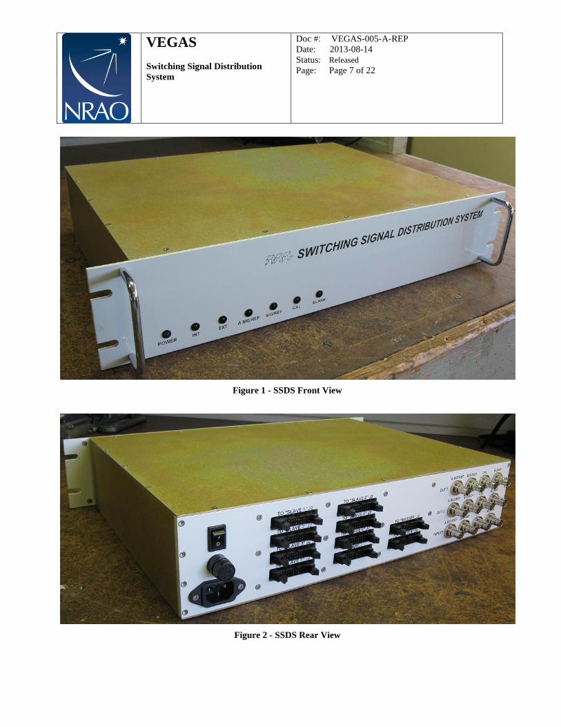
3 SSDS Electronics Design This section describes the electronics design of the SSDS. Figures 1 and 2 below show a fully assembled SSDS chassis.
VEGAS Switching Signal Distribution System
Doc #: VEGAS-005-A-REP Date: 2013-08-14 Status: Released Page: Page 7 of 22
Figure 1 - SSDS Front View
Figure 2 - SSDS Rear View
VEGAS Switching Signal Distribution System
Doc #: VEGAS-005-A-REP Date: 2013-08-14 Status: Released Page: Page 8 of 22
3.1 Theory of Operation The SSDS is responsible for insuring that all ROACH boards in the VEGAS Spectrometer receive precisely aligned, coherent switching state signals which, in turn, are used to accurately “bin” the data being processed. Normally, VEGAS will be configured such that a single ROACH serves as the “Switching Master”; and, as such, generates all the relevant switching state signals required by the entire system. These states are . . . Sig / Ref . . . A low level on this signal line indicates that the data being processed are that from a “live” source. A high level on this signal line indicates that the data being processed is from a “reference” source such as a calibrator. Please note that this signal is most often used in “position switching” observations. Cal . . . A low level on this signal line indicates that the data being processed is from a calibration source such as a noise diode located in a receiver’s front end. A high level on this signal line indicates that the noise source within the receiver has been switched off. Blank . . . A high level on this signal line indicates that the system is in the midst of a switching state transition and that the data being processed should be discarded. The SSDS receives these switching signals via a flat cable plugged into connector P15 on the “Switching Master” ROACH. It then utilizes low-skew, clock distribution chips along with flat cables which plug into the remaining “slave” ROACH boards’ connectors P13; thereby distributing the switching signals as necessary. The SSDS also has provisions for either “slaving” VEGAS to another Back End (which would provide the necessary switching signals) or “slaving” another Back End to VEGAS, in which case VEGAS would provide the necessary switching signals. These connections are accomplished via clearly labeled BNC connectors located on the SSDS’s back panel which are designed to utilize 50 ohm coaxial cables with all input and output signals being standard TTL levels.
VEGAS Switching Signal Distribution System
Doc #: VEGAS-005-A-REP Date: 2013-08-14 Status: Released Page: Page 9 of 22
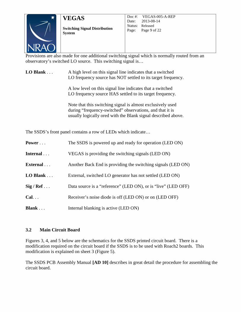
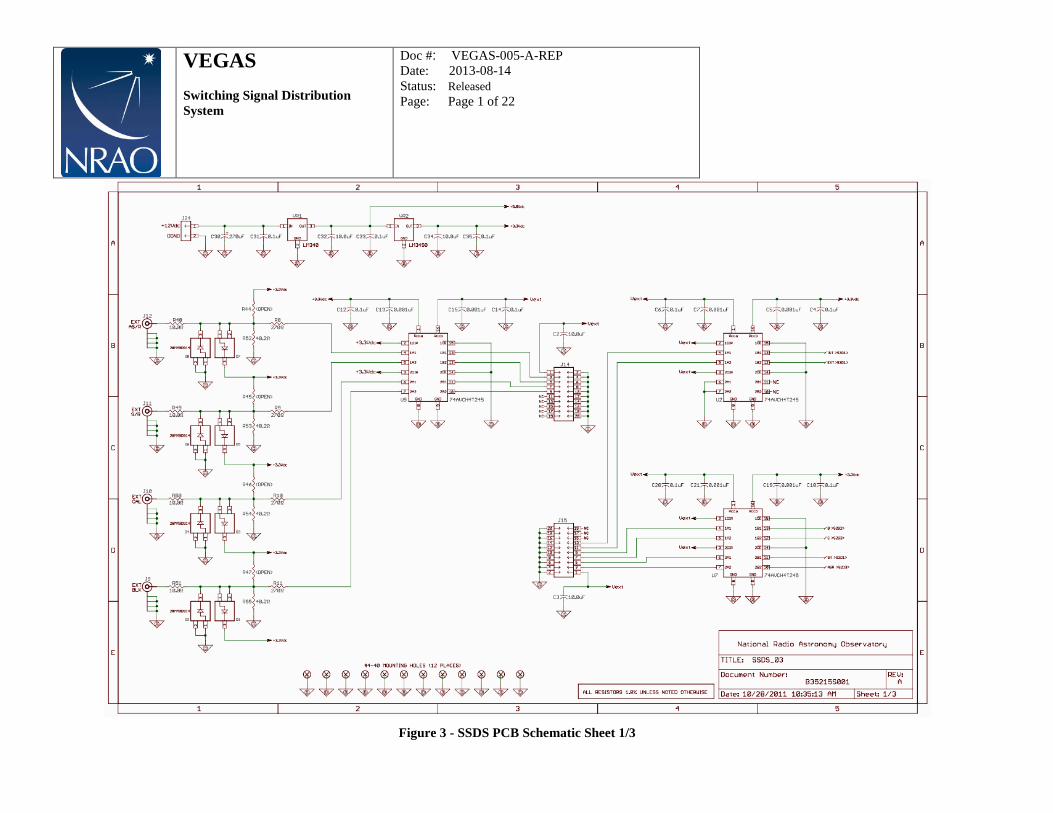
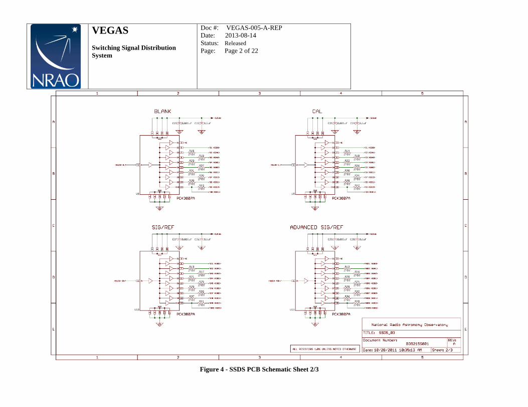
Provisions are also made for one additional switching signal which is normally routed from an observatory’s switched LO source. This switching signal is… LO Blank . . . A high level on this signal line indicates that a switched LO frequency source has NOT settled to its target frequency. A low level on this signal line indicates that a switched LO frequency source HAS settled to its target frequency. Note that this switching signal is almost exclusively used during “frequency-switched” observations, and that it is usually logically ored with the Blank signal described above. The SSDS’s front panel contains a row of LEDs which indicate… Power . . . The SSDS is powered up and ready for operation (LED ON) Internal . . . VEGAS is providing the switching signals (LED ON) External . . . Another Back End is providing the switching signals (LED ON) LO Blank . . . External, switched LO generator has not settled (LED ON) Sig / Ref . . . Data source is a “reference” (LED ON), or is “live” (LED OFF) Cal. . . Receiver’s noise diode is off (LED ON) or on (LED OFF) Blank . . . Internal blanking is active (LED ON) 3.2 Main Circuit Board Figures 3, 4, and 5 below are the schematics for the SSDS printed circuit board. There is a modification required on the circuit board if the SSDS is to be used with Roach2 boards. This modification is explained on sheet 3 (Figure 5). The SSDS PCB Assembly Manual [AD 10] describes in great detail the procedure for assembling the circuit board.
VEGAS Switching Signal Distribution System
Doc #: VEGAS-005-A-REP Date: 2013-08-14 Status: Released Page: Page 1 of 22
Figure 3 - SSDS PCB Schematic Sheet 1/3
VEGAS Switching Signal Distribution System
Doc #: VEGAS-005-A-REP Date: 2013-08-14 Status: Released Page: Page 2 of 22
Figure 4 - SSDS PCB Schematic Sheet 2/3
VEGAS Switching Signal Distribution System
Doc #: VEGAS-005-A-REP Date: 2013-08-14 Status: Released Page: Page 3 of 22
Figure 5 - SSDS PCB Schematic Sheet 3/3
VEGAS Switching Signal Distribution System
Doc #: VEGAS-005-A-REP Date: 2013-08-14 Status: Released Page: Page 1 of 22
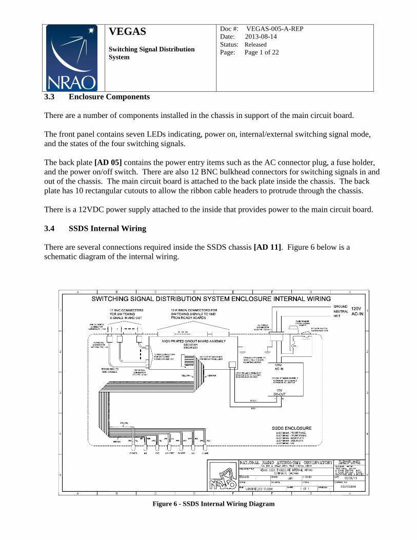
3.3 Enclosure Components There are a number of components installed in the chassis in support of the main circuit board. The front panel contains seven LEDs indicating, power on, internal/external switching signal mode, and the states of the four switching signals. The back plate [AD 05] contains the power entry items such as the AC connector plug, a fuse holder, and the power on/off switch. There are also 12 BNC bulkhead connectors for switching signals in and out of the chassis. The main circuit board is attached to the back plate inside the chassis. The back plate has 10 rectangular cutouts to allow the ribbon cable headers to protrude through the chassis. There is a 12VDC power supply attached to the inside that provides power to the main circuit board. 3.4 SSDS Internal Wiring There are several connections required inside the SSDS chassis [AD 11]. Figure 6 below is a schematic diagram of the internal wiring.
Figure 6 - SSDS Internal Wiring Diagram
VEGAS Switching Signal Distribution System
Doc #: VEGAS-005-A-REP Date: 2013-08-14 Status: Released Page: Page 2 of 22
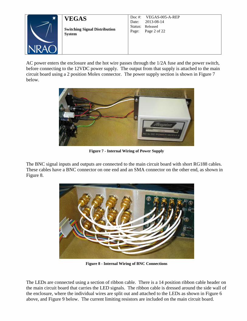
AC power enters the enclosure and the hot wire passes through the 1/2A fuse and the power switch, before connecting to the 12VDC power supply. The output from that supply is attached to the main circuit board using a 2 position Molex connector. The power supply section is shown in Figure 7 below.
Figure 7 - Internal Wiring of Power Supply
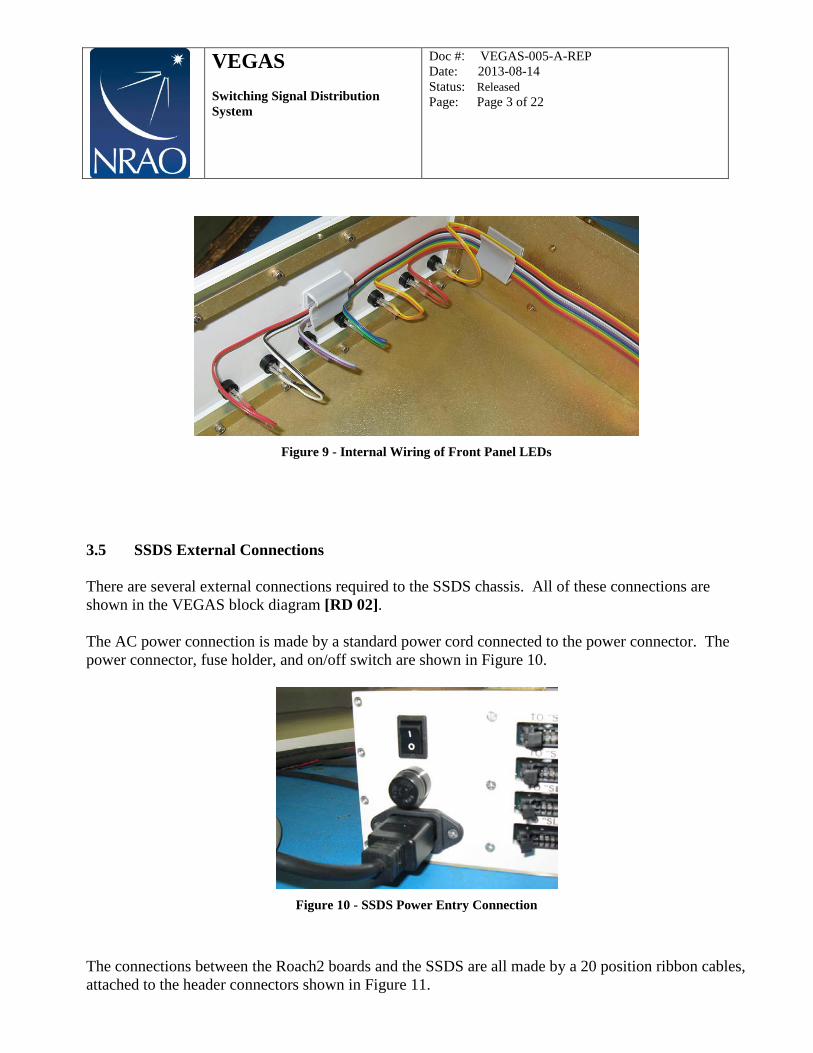
The BNC signal inputs and outputs are connected to the main circuit board with short RG188 cables. These cables have a BNC connector on one end and an SMA connector on the other end, as shown in Figure 8.
Figure 8 - Internal Wiring of BNC Connections
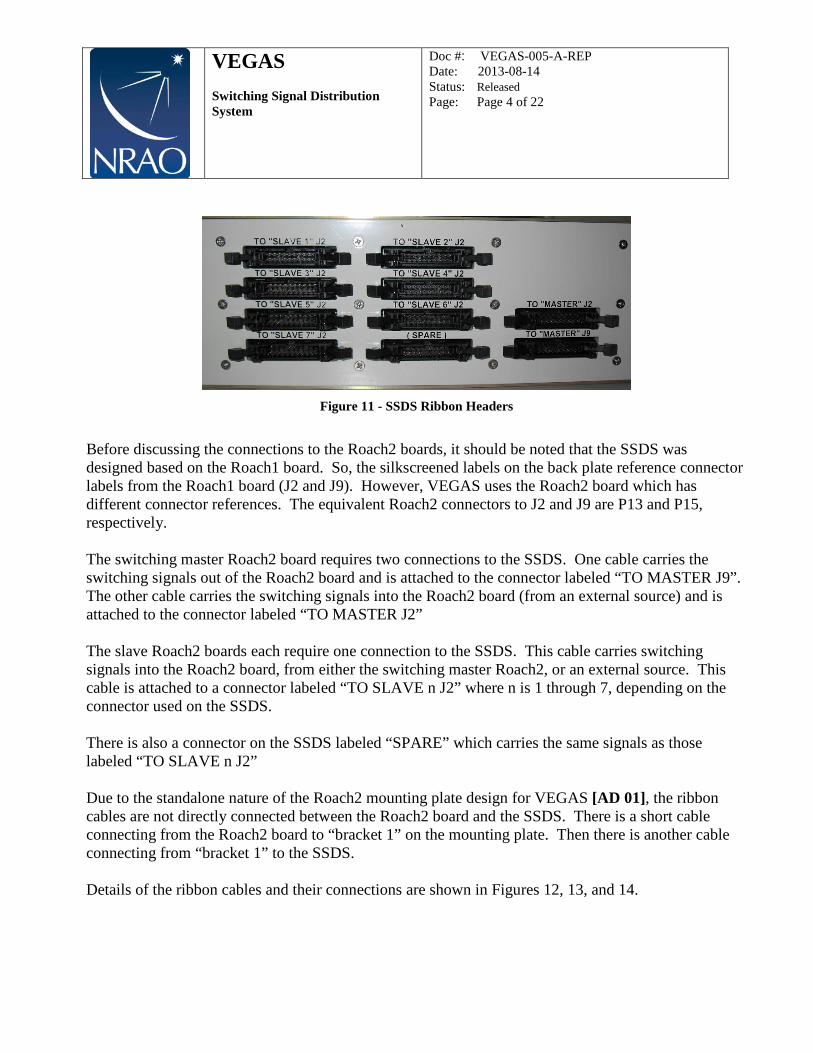
The LEDs are connected using a section of ribbon cable. There is a 14 position ribbon cable header on the main circuit board that carries the LED signals. The ribbon cable is dressed around the side wall of the enclosure, where the individual wires are split out and attached to the LEDs as shown in Figure 6 above, and Figure 9 below. The current limiting resistors are included on the main circuit board.
VEGAS Switching Signal Distribution System
Doc #: VEGAS-005-A-REP Date: 2013-08-14 Status: Released Page: Page 3 of 22
Figure 9 - Internal Wiring of Front Panel LEDs
3.5 SSDS External Connections There are several external connections required to the SSDS chassis. All of these connections are shown in the VEGAS block diagram [RD 02]. The AC power connection is made by a standard power cord connected to the power connector. The power connector, fuse holder, and on/off switch are shown in Figure 10.
Figure 10 - SSDS Power Entry Connection
The connections between the Roach2 boards and the SSDS are all made by a 20 position ribbon cables, attached to the header connectors shown in Figure 11.
VEGAS Switching Signal Distribution System
Doc #: VEGAS-005-A-REP Date: 2013-08-14 Status: Released Page: Page 4 of 22
Figure 11 - SSDS Ribbon Headers
Before discussing the connections to the Roach2 boards, it should be noted that the SSDS was designed based on the Roach1 board. So, the silkscreened labels on the back plate reference connector labels from the Roach1 board (J2 and J9). However, VEGAS uses the Roach2 board which has different connector references. The equivalent Roach2 connectors to J2 and J9 are P13 and P15, respectively. The switching master Roach2 board requires two connections to the SSDS. One cable carries the switching signals out of the Roach2 board and is attached to the connector labeled “TO MASTER J9”. The other cable carries the switching signals into the Roach2 board (from an external source) and is attached to the connector labeled “TO MASTER J2” The slave Roach2 boards each require one connection to the SSDS. This cable carries switching signals into the Roach2 board, from either the switching master Roach2, or an external source. This cable is attached to a connector labeled “TO SLAVE n J2” where n is 1 through 7, depending on the connector used on the SSDS. There is also a connector on the SSDS labeled “SPARE” which carries the same signals as those labeled “TO SLAVE n J2” Due to the standalone nature of the Roach2 mounting plate design for VEGAS [AD 01], the ribbon cables are not directly connected between the Roach2 board and the SSDS. There is a short cable connecting from the Roach2 board to “bracket 1” on the mounting plate. Then there is another cable connecting from “bracket 1” to the SSDS. Details of the ribbon cables and their connections are shown in Figures 12, 13, and 14.

VEGAS Switching Signal Distribution System
Doc #: VEGAS-005-A-REP Date: 2013-08-14 Status: Released Page: Page 5 of 22
Figure 12 - SSDS Ribbon Cable, SSDS to Bracket1

VEGAS Switching Signal Distribution System
Doc #: VEGAS-005-A-REP Date: 2013-08-14 Status: Released Page: Page 6 of 22
Figure 13 - SSDS Ribbon Cables, Bracket1 to Roach2
VEGAS Switching Signal Distribution System
Doc #: VEGAS-005-A-REP Date: 2013-08-14 Status: Released Page: Page 7 of 22
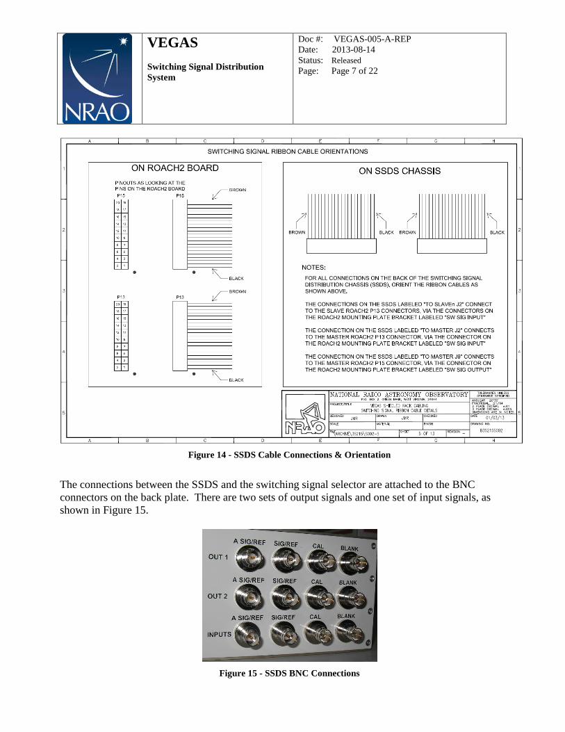
Figure 14 - SSDS Cable Connections & Orientation
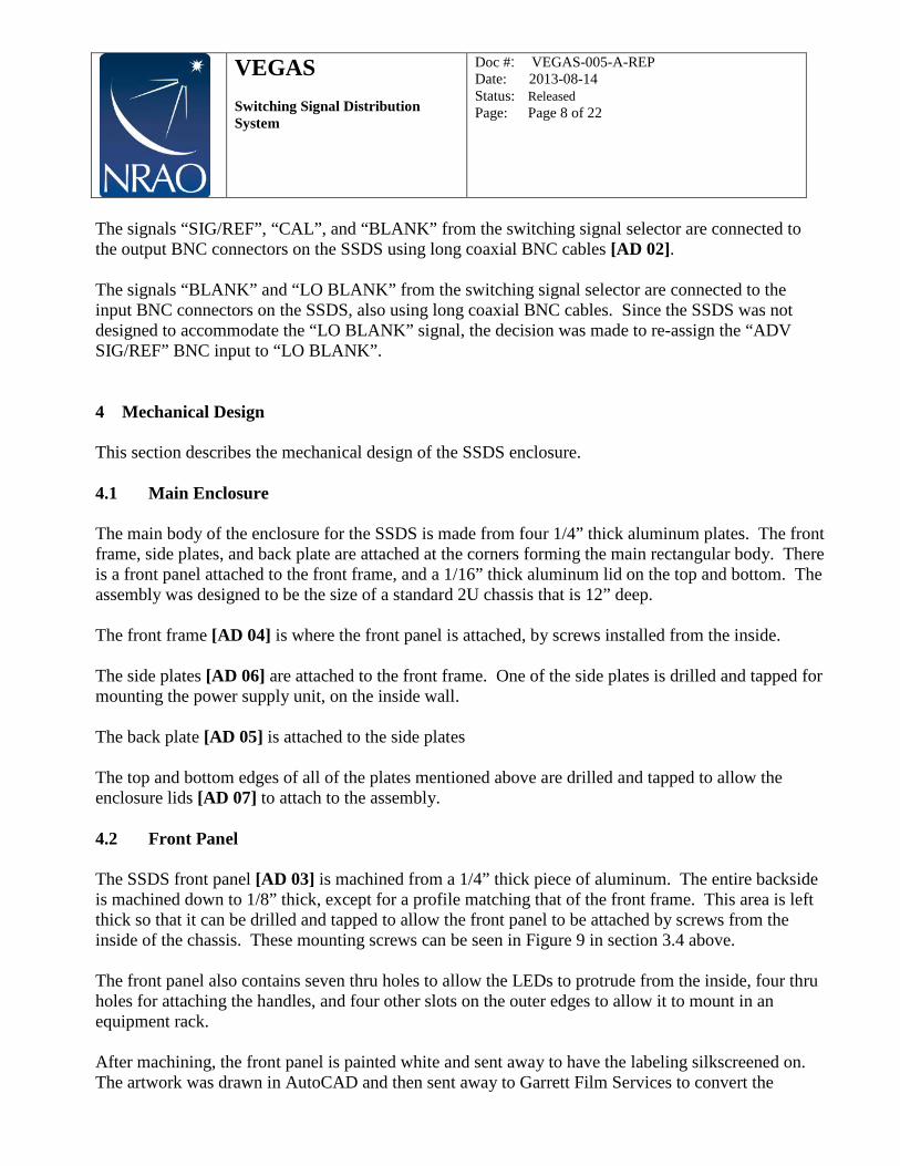
The connections between the SSDS and the switching signal selector are attached to the BNC connectors on the back plate. There are two sets of output signals and one set of input signals, as shown in Figure 15.
Figure 15 - SSDS BNC Connections
VEGAS Switching Signal Distribution System
Doc #: VEGAS-005-A-REP Date: 2013-08-14 Status: Released Page: Page 8 of 22
The signals “SIG/REF”, “CAL”, and “BLANK” from the switching signal selector are connected to the output BNC connectors on the SSDS using long coaxial BNC cables [AD 02]. The signals “BLANK” and “LO BLANK” from the switching signal selector are connected to the input BNC connectors on the SSDS, also using long coaxial BNC cables. Since the SSDS was not designed to accommodate the “LO BLANK” signal, the decision was made to re-assign the “ADV SIG/REF” BNC input to “LO BLANK”. 4 Mechanical Design This section describes the mechanical design of the SSDS enclosure. 4.1 Main Enclosure The main body of the enclosure for the SSDS is made from four 1/4” thick aluminum plates. The front frame, side plates, and back plate are attached at the corners forming the main rectangular body. There is a front panel attached to the front frame, and a 1/16” thick aluminum lid on the top and bottom. The assembly was designed to be the size of a standard 2U chassis that is 12” deep. The front frame [AD 04] is where the front panel is attached, by screws installed from the inside. The side plates [AD 06] are attached to the front frame. One of the side plates is drilled and tapped for mounting the power supply unit, on the inside wall. The back plate [AD 05] is attached to the side plates The top and bottom edges of all of the plates mentioned above are drilled and tapped to allow the enclosure lids [AD 07] to attach to the assembly. 4.2 Front Panel The SSDS front panel [AD 03] is machined from a 1/4” thick piece of aluminum. The entire backside is machined down to 1/8” thick, except for a profile matching that of the front frame. This area is left thick so that it can be drilled and tapped to allow the front panel to be attached by screws from the inside of the chassis. These mounting screws can be seen in Figure 9 in section 3.4 above. The front panel also contains seven thru holes to allow the LEDs to protrude from the inside, four thru holes for attaching the handles, and four other slots on the outer edges to allow it to mount in an equipment rack. After machining, the front panel is painted white and sent away to have the labeling silkscreened on. The artwork was drawn in AutoCAD and then sent away to Garrett Film Services to convert the
VEGAS Switching Signal Distribution System
Doc #: VEGAS-005-A-REP Date: 2013-08-14 Status: Released Page: Page 9 of 22
AutoCAD file into a 1:1 photoplot. This photoplot, along with the panels, were sent to WWW Electronics for the silkscreen application. 4.3 Back Plate The back plate contains many cutouts and features for attaching the various components described above. The cutouts for the ribbon headers were made larger than specified in the datasheet to allow the ejector tabs to be functional. There is also a 0.200” deep recessed area machined on the inside wall surrounding the ribbon header cutouts to help reduce the mounting depth of the ribbon headers. The combination of the mounting depth and the back plate thickness required these changes, otherwise the ejector tabs could not rotate far enough to release the connectors. The cutouts for the AC power connector, fuse holder, toggle switch, and BNC cables were all made per their datasheets. There is a recessed area machined on the inside wall of the back plate around the toggle switch cutout. This was to reduce the panel thickness to 1/16” inch per the datasheet for the switch. Similar to the front panel, rear panel is painted white, and the labeling is silkscreened on. 5 RFI/EMI Considerations The SSDS is not constructed in a shielded enclosure. Given that it is an integrated component of VEGAS, the SSDS is installed in the shielded rack, which resides in the shielded equipment room. No additional RFI mitigation is necessary.
VEGAS Switching Signal Distribution System
Doc #: VEGAS-005-A-REP Date: 2013-08-14 Status: Released Page: Page 10 of 22
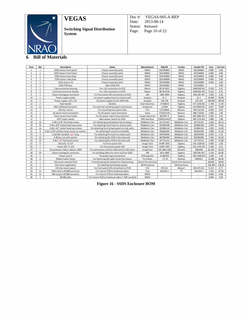
6 Bill of Materials
Item Qty Description Notes Manufacturer Mfg PN Vendor Vendor PN Cost Ext Cost1 1 SSDS chassis front panel Chassis assembly parts NRAO 35215M001 NRAO 35215M001 0.000 0.002 1 SSDS chassis front frame Chassis assembly parts NRAO 35215M002 NRAO 35215M002 0.000 0.003 1 SSDS chassis back plate Chassis assembly parts NRAO 35215M003 NRAO 35215M003 0.000 0.004 2 SSDS chassis side plate Chassis assembly parts NRAO 35215M004 NRAO 35215M004 0.000 0.005 2 SSDS chassis lid Chassis assembly parts NRAO 35215M005 NRAO 35215M005 0.000 0.006 1 SSDS PCB Assy Main SSDS PCB NRAO 35215Q001 NRAO 35215Q001 0.007 1 2 pos connector housing For +12V connection to PCB Molex 09-50-3021 Digikey WM2100-ND 0.320 0.328 2 Connector terminal, female For +12V connection to PCB Molex 08-50-0134 Digikey WM2303-ND 0.153 0.319 1 14 pos rectangular connector For front panel LED connections to PCB 3M 3385-6000 Digikey MSC14K-ND 3.360 3.3610 1 Power supply socket For power supply mount to chassis wall Acopian EL-1 Acopian EL-1 20.000 20.0011 1 Power supply, 12V 1.2A DC power supply for the SSDS PCB Acopian 12E-120 Acopian 12E-120 149.000 149.0012 2 Rack Handle Handles Bud Industries H-9168-B Digikey 377-1236-ND 5.700 11.4013 12 BNC bulkhead connector For external switching signal connections Amphenol 112434 Digikey ACX1844-ND 6.657 79.8914 7 LED clip mount For mounting front panel LEDs VCC CLP126BLK Mouser 593-CLP126 0.090 0.6315 1 AC panel mount receptacle For AC power input connection Volex 17252A 0 B1 Mouser 686-17252A 1.830 1.8316 1 Panel mount fuse holder For AC power input fuse protection Cooper Bussman BK/HKP-R Digikey 283-2850-ND 5.430 5.4317 1 SPST rocker switch Main power switch for SSDS NKK Switches CWSB11AA2F Digikey 360-1724-ND 2.860 2.8618 16 4-40 x 5/16" flat head screws For attaching top & bottom lids to chassis McMaster Carr 91771A107 McMaster Carr 91771A107 4.320 69.1219 26 4-40 x 3/8" socket head cap screws For attaching front frame to chassis walls McMaster Carr 92196A108 McMaster Carr 92196A108 2.870 74.6220 16 4-40 x 1/2" socket head cap screws For attaching front & back panels to side walls McMaster Carr 92196A110 McMaster Carr 92196A110 3.250 52.0021 4 6-32 x 5/16" phillips head screws w/ washer For attaching PS mount to standoffs McMaster Carr 95345A045 McMaster Carr 95345A045 7.800 31.2022 4 6-32 M/F standoff, 3/4" long For attaching PS mount to chassis wall McMaster Carr 91075A444 McMaster Carr 91075A444 0.440 1.7623 12 4-40 hex nut with washer For attaching the PCB to the back wall McMaster Carr 96278A005 McMaster Carr 96278A005 5.450 65.4024 12 4-40 x 5/8" flat head screws For attaching the PCB to the back wall McMaster Carr 91771A112 McMaster Carr 91771A112 4.390 52.6825 6 Red LED, T1-3/4 For front panel LEDs Avago Tech HLMP-3301 Digikey 516-1328-ND 0.306 1.8426 1 Green LED, T1-3/4 For front panel power LED Avago Tech HLMP-3507 Digikey 516-1333-ND 0.306 0.3127 1 20 conductor ribbon cablem, 100ft For connections to/from SSDS and for LED conns Amphenol 135-2801-020 Newark 78K6398 81.920 81.9228 20 20 pos rectangular connector For building cables for conns to/from SSDS 3M 3421-6000 Digikey MSC20K-ND 3.150 63.0029 1 Power cord, 6' AC power input connection Phihong USA AC30UNA Digikey 993-1039-ND 3.180 3.1830 4 Ribbon Cable Clamp For fastening LED cable inside the chassis Pro Power FC-25 Newark 24M2011 11.600 46.4031 1 Silk screen artwork films Front & back panel artwork for silkscreening Garret Film Services - Garret Film Services - 68.000 68.0032 1 Silk screen application For labeling front & back panels 3W Electronics - 3W Electronics - 118.200 118.2033 7 LED clip mount spacer For front panel LED connections to PCB VCC SPC125 Mouser 593-SPC125 0.110 0.7734 12 SMA male to RG188 connector For interior PCB to bulkhead cables Tyco 1051654-1 TTI 1051654-1 7.250 87.0035 12 BNC plug to RG188 connector For interior PCB to bulkhead cables NRAO - - - 0.000 0.0036 1 RG188 cable For interior PCB to bulkhead cables (~10ft needed) NRAO - - - 0.000 0.00
Figure 16 - SSDS Enclosure BOM