vel tech high tech dr.ranagarajan dr.sakunthala engineering … · 2019-11-22 · vel tech high...
TRANSCRIPT
Vel Tech High Tech Dr.Ranagarajan Dr.Sakunthala Engineering College – Department of ECE
Page | 1
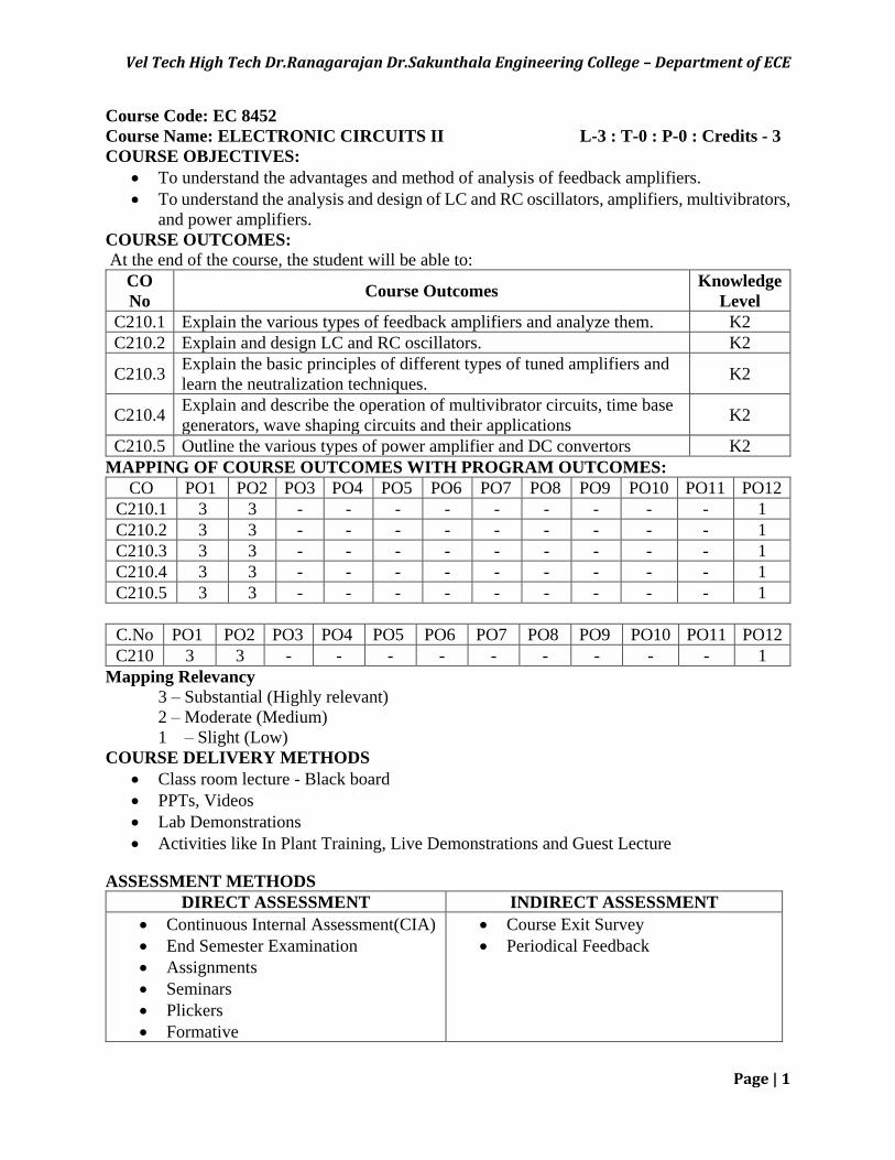
Course Code: EC 8452
Course Name: ELECTRONIC CIRCUITS II L-3 : T-0 : P-0 : Credits - 3
COURSE OBJECTIVES:
To understand the advantages and method of analysis of feedback amplifiers.
To understand the analysis and design of LC and RC oscillators, amplifiers, multivibrators,
and power amplifiers.
COURSE OUTCOMES:
At the end of the course, the student will be able to:
CO
No Course Outcomes
Knowledge
Level
C210.1 Explain the various types of feedback amplifiers and analyze them. K2
C210.2 Explain and design LC and RC oscillators. K2
C210.3 Explain the basic principles of different types of tuned amplifiers and
learn the neutralization techniques. K2
C210.4 Explain and describe the operation of multivibrator circuits, time base
generators, wave shaping circuits and their applications K2
C210.5 Outline the various types of power amplifier and DC convertors K2
MAPPING OF COURSE OUTCOMES WITH PROGRAM OUTCOMES:
CO PO1 PO2 PO3 PO4 PO5 PO6 PO7 PO8 PO9 PO10 PO11 PO12
C210.1 3 3 - - - - - - - - - 1
C210.2 3 3 - - - - - - - - - 1
C210.3 3 3 - - - - - - - - - 1
C210.4 3 3 - - - - - - - - - 1
C210.5 3 3 - - - - - - - - - 1
C.No PO1 PO2 PO3 PO4 PO5 PO6 PO7 PO8 PO9 PO10 PO11 PO12
C210 3 3 - - - - - - - - - 1
Mapping Relevancy
3 – Substantial (Highly relevant)
2 – Moderate (Medium)
1 – Slight (Low)
COURSE DELIVERY METHODS
Class room lecture - Black board
PPTs, Videos
Lab Demonstrations
Activities like In Plant Training, Live Demonstrations and Guest Lecture
ASSESSMENT METHODS
DIRECT ASSESSMENT INDIRECT ASSESSMENT
Continuous Internal Assessment(CIA)
End Semester Examination
Assignments
Seminars
Plickers
Formative
Course Exit Survey
Periodical Feedback
Vel Tech High Tech Dr.Ranagarajan Dr.Sakunthala Engineering College – Department of ECE
Page | 2
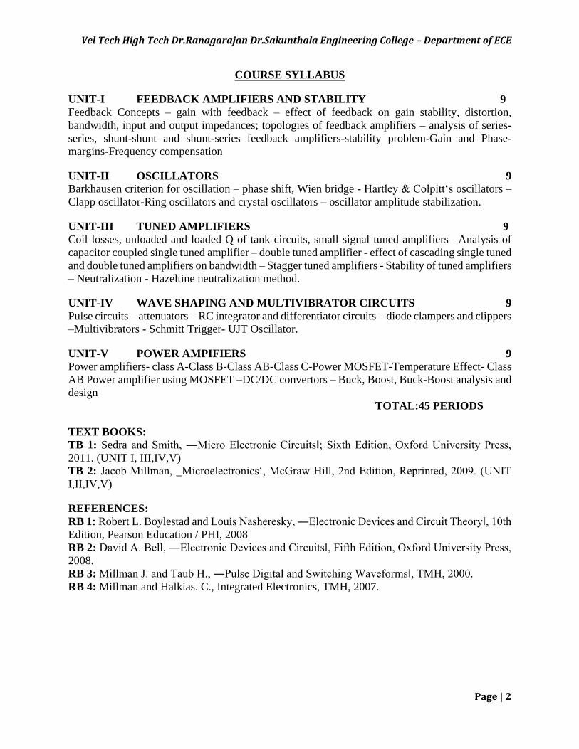
COURSE SYLLABUS
UNIT-I FEEDBACK AMPLIFIERS AND STABILITY 9
Feedback Concepts – gain with feedback – effect of feedback on gain stability, distortion,
bandwidth, input and output impedances; topologies of feedback amplifiers – analysis of series-
series, shunt-shunt and shunt-series feedback amplifiers-stability problem-Gain and Phase-
margins-Frequency compensation
UNIT-II OSCILLATORS 9
Barkhausen criterion for oscillation – phase shift, Wien bridge - Hartley & Colpitt‘s oscillators –
Clapp oscillator-Ring oscillators and crystal oscillators – oscillator amplitude stabilization.
UNIT-III TUNED AMPLIFIERS 9
Coil losses, unloaded and loaded Q of tank circuits, small signal tuned amplifiers –Analysis of
capacitor coupled single tuned amplifier – double tuned amplifier - effect of cascading single tuned
and double tuned amplifiers on bandwidth – Stagger tuned amplifiers - Stability of tuned amplifiers
– Neutralization - Hazeltine neutralization method.
UNIT-IV WAVE SHAPING AND MULTIVIBRATOR CIRCUITS 9
Pulse circuits – attenuators – RC integrator and differentiator circuits – diode clampers and clippers
–Multivibrators - Schmitt Trigger- UJT Oscillator.
UNIT-V POWER AMPIFIERS 9
Power amplifiers- class A-Class B-Class AB-Class C-Power MOSFET-Temperature Effect- Class
AB Power amplifier using MOSFET –DC/DC convertors – Buck, Boost, Buck-Boost analysis and
design
TOTAL:45 PERIODS
TEXT BOOKS:
TB 1: Sedra and Smith, ―Micro Electronic Circuits‖; Sixth Edition, Oxford University Press,
2011. (UNIT I, III,IV,V)
TB 2: Jacob Millman, ‗Microelectronics‘, McGraw Hill, 2nd Edition, Reprinted, 2009. (UNIT
I,II,IV,V)
REFERENCES:
RB 1: Robert L. Boylestad and Louis Nasheresky, ―Electronic Devices and Circuit Theory‖, 10th
Edition, Pearson Education / PHI, 2008
RB 2: David A. Bell, ―Electronic Devices and Circuits‖, Fifth Edition, Oxford University Press,
2008.
RB 3: Millman J. and Taub H., ―Pulse Digital and Switching Waveforms‖, TMH, 2000.
RB 4: Millman and Halkias. C., Integrated Electronics, TMH, 2007.
Vel Tech High Tech Dr.Ranagarajan Dr.Sakunthala Engineering College – Department of ECE
Page | 3
COURSE DELIVERY PLAN
S.
No Date Unit Topic
Text/
Refer
ence
Books
Teaching
Methodology
Cours
e
Outco
me
1 17.12.18 I Feedback Concepts
TB1,
RB1
Class room
lecture -
Black board/
Plickers
CO1
2 17.12.18 I gain with feedback CO1
3 18.12.18 I effect of feedback on gain
stability, distortion CO1
Slip Test 1
4 18.12.18 I bandwidth Class room
lecture -
Black board
CO1
5 19.12.18 I input and output impedances CO1
6 19.12.18 I topologies of feedback amplifiers CO1
Slip Test 2
7 20.12.18 I analysis of series-series
Class room
lecture -
Black board/
Plickers
CO1
8 20.12.18 I shunt-shunt CO1
9 21.12.18 I shunt-series feedback amplifiers CO1
10 21.12.18 I stability problem CO1
11 22.12.18 I Gain and Phase-margins CO1
12 24.12.18 I Frequency compensation CO1
13 2612.18 I Problems CO1
14 26.12.18 I Revision class on previous years
university question papers CO1
UEPS/CIA-I
13 5.1.19 II Barkhausen criterion for
oscillation
TB1
Class room
lecture -
Black board/
Plickers/PPT
CO2
14 7.1.19 II phase shift CO2
15 8.1.19 II Wien bridge CO2
Slip Test 3
16 9.1.19 II Hartley Class room
lecture -
Black board
and lab demo
CO2
17 10.1.19 II Colpitt‘s oscillators CO2
18 11.1.19 II Clapp oscillator CO2
Slip Test 4
19 12.1.19 II Ring oscillators Class room
lecture -
Black board
and lab demo
CO2
UEPS/CIA-II
20 18.1.19 II crystal oscillators CO2
21 19.1.19 II oscillator amplitude CO2
COURSE INSTRUCTOR Mrs.K.SHANMUGA
PRIYA FACULTY ID HTS1242
COURSE NAME Electronic Circuits-II COURSE CODE EC8452
YEAR/SEM II/ IV MONTH & YEAR DEC- 2018
Vel Tech High Tech Dr.Ranagarajan Dr.Sakunthala Engineering College – Department of ECE
Page | 4
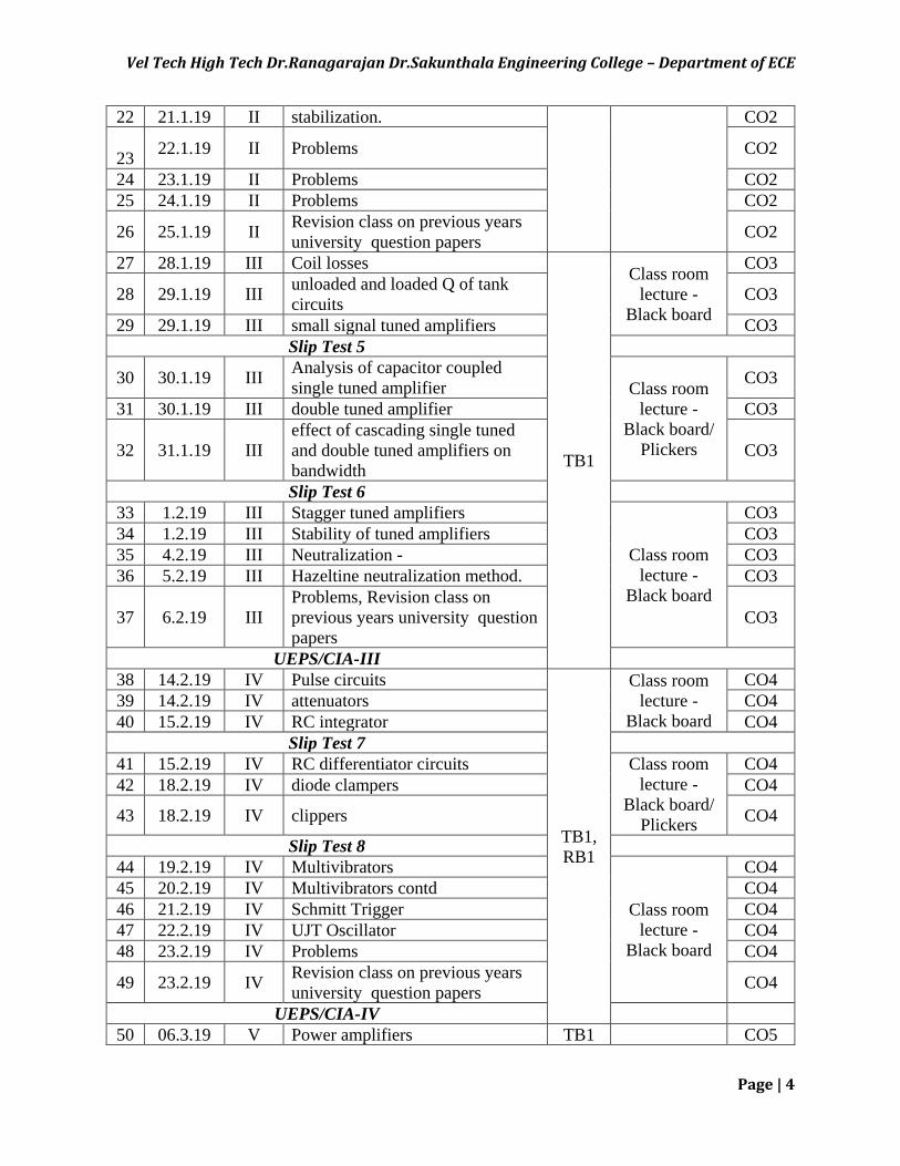
22 21.1.19 II stabilization. CO2
23 22.1.19 II Problems CO2
24 23.1.19 II Problems CO2
25 24.1.19 II Problems CO2
26 25.1.19 II Revision class on previous years
university question papers CO2
27 28.1.19 III Coil losses
TB1
Class room
lecture -
Black board
CO3
28 29.1.19 III unloaded and loaded Q of tank
circuits CO3
29 29.1.19 III small signal tuned amplifiers CO3
Slip Test 5
30 30.1.19 III Analysis of capacitor coupled
single tuned amplifier Class room
lecture -
Black board/
Plickers
CO3
31 30.1.19 III double tuned amplifier CO3
32 31.1.19 III
effect of cascading single tuned
and double tuned amplifiers on
bandwidth
CO3
Slip Test 6
33 1.2.19 III Stagger tuned amplifiers
Class room
lecture -
Black board
CO3
34 1.2.19 III Stability of tuned amplifiers CO3
35 4.2.19 III Neutralization - CO3
36 5.2.19 III Hazeltine neutralization method. CO3
37 6.2.19 III
Problems, Revision class on
previous years university question
papers
CO3
UEPS/CIA-III
38 14.2.19 IV Pulse circuits
TB1,
RB1
Class room
lecture -
Black board
CO4
39 14.2.19 IV attenuators CO4
40 15.2.19 IV RC integrator CO4
Slip Test 7
41 15.2.19 IV RC differentiator circuits Class room
lecture -
Black board/
Plickers
CO4
42 18.2.19 IV diode clampers CO4
43 18.2.19 IV clippers CO4
Slip Test 8
44 19.2.19 IV Multivibrators
Class room
lecture -
Black board
CO4
45 20.2.19 IV Multivibrators contd CO4
46 21.2.19 IV Schmitt Trigger CO4
47 22.2.19 IV UJT Oscillator CO4
48 23.2.19 IV Problems CO4
49 23.2.19 IV Revision class on previous years
university question papers CO4
UEPS/CIA-IV
50 06.3.19 V Power amplifiers TB1 CO5
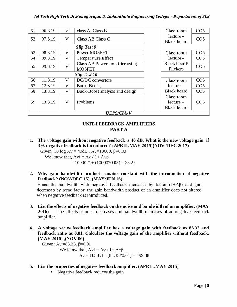
Vel Tech High Tech Dr.Ranagarajan Dr.Sakunthala Engineering College – Department of ECE
Page | 5
51 06.3.19 V class A ,Class B Class room
lecture -
Black board
CO5
52 07.3.19 V Class AB,Class C CO5
Slip Test 9
53 08.3.19 V Power MOSFET Class room
lecture -
Black board/
Plickers
CO5
54 09.3.19 V Temperature Effect CO5
55 09.3.19 V Class AB Power amplifier using
MOSFET CO5
Slip Test 10
56 11.3.19 V DC/DC convertors Class room
lecture –
Black board
CO5
57 12.3.19 V Buck, Boost, CO5
58 13.3.19 V Buck-Boost analysis and design CO5
59 13.3.19 V Problems
Class room
lecture –
Black board
CO5
UEPS/CIA-V
UNIT-I FEEDBACK AMPLIFIERS
PART A
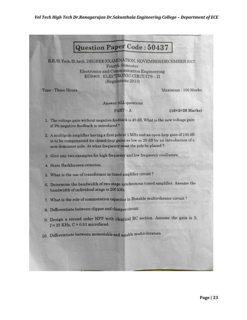
1. The voltage gain without negative feedback is 40 dB. What is the new voltage gain if
3% negative feedback is introduced? (APRIL/MAY 2015)(NOV /DEC 2017)
Given: 10 log Av = 40dB , AV=10000, β=0.03
We know that, Avf = AV / 1+ AVβ
=10000 /1+ (10000*0.03) = 33.22
2. Why gain bandwidth product remains constant with the introduction of negative
feedback? (NOV/DEC 15), (MAY/JUN 16)
Since the bandwidth with negative feedback increases by factor (1+Aβ) and gain
decreases by same factor, the gain bandwidth product of an amplifier does not altered,
when negative feedback is introduced.
3. List the effects of negative feedback on the noise and bandwidth of an amplifier. (MAY
2016) The effects of noise decreases and bandwidth increases of an negative feedback
amplifier.
4. A voltage series feedback amplifier has a voltage gain with feedback as 83.33 and
feedback ratio as 0.01. Calculate the voltage gain of the amplifier without feedback.
(MAY 2016) ,(NOV 06)
Given: AVf=83.33, β=0.01
We know that, Avf = AV / 1+ AVβ
AV =83.33 /1+ (83.33*0.01) = 499.88
5. List the properties of negative feedback amplifier. (APRIL/MAY 2015)
• Negative feedback reduces the gain
Vel Tech High Tech Dr.Ranagarajan Dr.Sakunthala Engineering College – Department of ECE
Page | 6
• Reduction in noise
• Reduction in non linear distortion
• Bandwidth improvement
• Gain Desensitivity
6. State nyquist stability criterion. (APRIL/MAY 2015),(NOV/DEC 2010)
The plot which shows the relationship between gain and phase-shift as a function of frequency
is called as nyquist diagram.
• The amplifier is unstable if the curve encloses the point -1+j0. The system is called
as unstable system.
• The amplifier is stable if the curve encloses the point -1+jo. That system is called as
stable system.
7. ‘Negative feedback stabilizes the gain’-justify the statement. (MAY/JUN 2014)
The gain with negative feedback is given as:
Af = A / 1+ Aβ
If Aβ>> 1 Then Af =1/ β
Since Af is dependent on feedback factor β the gain with negative feedback is said to be
stabilized.
8. What is the effect of negative feedback on circuit noise? (APRIL/MAY 2017) The effects
of noise decreases of an negative feedback amplifier.
9. A feedback amplifier has an open loop gain of 600 and feedback factor β = 0.01. Find
the closed loop gain with Negative feedback. (NOV/DEC 2014)
Given: Avf = AV/ 1+ AV β
=600/(1+600*0.01)
=85.714.
10. What is meant by Negative feedback? Mention its advantages. (NOV/DEC 2013)
(NOV/DEC 2014) (APRIL/MAY 2015)
If the feedback signal is out of phase with the input signal then the input voltage
applied to the basic amplifier is decreased and correspondingly the output is decreased.
This type of feedback is known as negative or degenerative feedback.
11. What is the effect on input and output impedance of an amplifier if it employs voltage
series negative feedback? (APRIL/MAY 2013)
In voltage series feedback, the input resistance increases and output resistance decreases.
12. Write the expression for the gain of an amplifier with feedback. (NOV/DEC 2013) Avf
= AV/ 1+ AV β
Where, Avf – feedback voltage gain.
AV – Voltage gain. β - Feedback factor
Vel Tech High Tech Dr.Ranagarajan Dr.Sakunthala Engineering College – Department of ECE
Page | 7
13. What is loop gain or return ratio. (MAY 11, DEC 11)
A path of a signal from input terminals through basic amplifier, through the feedback
network and back to the input terminals forms a loop. The gain of this loop is the product
-A β . This gain is known as loop gain or return ratio.
14. Voltage gain of an amplifier without feedback is 60dB. It decreases to 40dB with
feedback.
Calculate the feedback factor.
Solution: Given: Av = 60dB and Avf = 40 dB. We know that,
Avf = AV / 1+ AVβ β = (AV- Avf) / ( AVAvf) = (60-40) / (60*40)
β = 0.00833
PART-B
1. Explain how negative feedback acts on loop gain, frequency, distortion, Input
Impedance and output Impedance of a circuit. (APR 2010)
Refer:. Sedra and Smith, “Micro Electronic Circuits”;Page No.:715
2. With block diagram of current series feedback and derive the expression RIF
and ROF.(NOV/DEC 2016)
Refer:. Sedra and Smith, “Micro Electronic Circuits”;Page No.:738
3. Explain Nyquist criterion to analyse the stability of feedback amplifiers. (APR
2010) Refer:. Sedra and Smith, “Micro Electronic Circuits”;Page No.:755
4. Draw the circuit of an emitter follower. Identify the type of negative feedback
and calculate the gain, input and output resistance with and without feedback.
(NOV 2013)
Refer:. Sedra and Smith, “Micro Electronic Circuits”;Page No.:731
5. Explain the current shunt feedback amplifier with a neat diagram. (APR 2011)
Refer:. Sedra and Smith, “Micro Electronic Circuits”;Page No.:738
6. Give the schematic representation of a single loop feedback amplifier. (NOV
2012) Refer:. Sedra and Smith, “Micro Electronic Circuits”;Page No.:712
7. An amplifier has a midband gain of 125 and a bandwidth of 250Khz. (APR
2010) (i)What will be the new bandwidth and gain, if 4% negative feedback is
introduced?
(ii)What should be the amount of feedback, if the bandwidth is to be restricted to
1Mhz? Refer:. Sedra and Smith, “Micro Electronic Circuits”;Page No.:780
8. Explain the steps to be carried out for complete analysis of a feedback amplifier.
(APR 2013) Refer:. Sedra and Smith, “Micro Electronic Circuits”;Page No.:722
Vel Tech High Tech Dr.Ranagarajan Dr.Sakunthala Engineering College – Department of ECE
Page | 8
9. Explain current series and voltage shunt feedback connections. (APR 2010)
Refer:. Sedra and Smith, “Micro Electronic Circuits”;Page No.:738
10. Sketch the block diagram of a feedback amplifier and derive the expressions for
gain with negative feedback and also explain input and output resistance.
(NOV 2012) Refer:. Sedra and Smith, “Micro Electronic Circuits”;Page No.:715
11. Determine the voltage gain, input impedance and output impedance of
transistor based current series feedback amplifier.(NOV 2014)
Refer:. Sedra and Smith, “Micro Electronic Circuits”;Page No.:738
12. Compare the effects of four feedback topologies on amplifiers.(NOV 2014)
Refer:. Sedra and Smith, “Micro Electronic Circuits”;Page No.:718
13. Explain the voltage shunt feedback amplifier with a neat diagram. (NOV 2012)
Refer:. Sedra and Smith, “Micro Electronic Circuits”;Page No.:722
14. The distortion in an amplifier is found to be 3%, when the feedback ratio of
negative feedback amplifier is 0.04. When the feedback is removed, the
distortion becomes 15%. Find the open and closed loop gain. (APR 2010)
Refer:. Sedra and Smith, “Micro Electronic Circuits”;Page No.:780
15. Elaborate the methods to identifying the feedback amplifier. (APR 2013) Refer:.
Sedra and Smith, “Micro Electronic Circuits”;Page No.:718
16. Explain voltage series and current shunt feedback connections. (APR 2010)
Refer:. Sedra and Smith, “Micro Electronic Circuits”;Page No.:738/731
UNIT-II OSCILLATORS
PART A
1. State the Barkhausen criterion for an oscillator.(APRIL/MAY 15),(MAY/JUN 14),
(NOV/DEC 14) , (MAY/JUN 12) , (NOV/DEC 11) ,(APRIL/MAY 10)
• The total phase shift around a loop, as the signal proceeds from input through
amplifier, feedback network back to input again, completing a loop, is precisely 00
or 3600.
• The magnitude of the product of the open loop gain of the amplifier (A) and the
feedback factor β is unity. i.e., A β = 1.
2. What is the major disadvantage of a twin –t oscillator? (MAY/JUN 16)
• Oscillation cannot occur at frequencies above or below because of the negative
feedback through the filters.
• At however, there is negligible negative feedback; thus, the positive feedback through
the voltage divider and allows the circuit to oscillate.
Vel Tech High Tech Dr.Ranagarajan Dr.Sakunthala Engineering College – Department of ECE
Page | 9
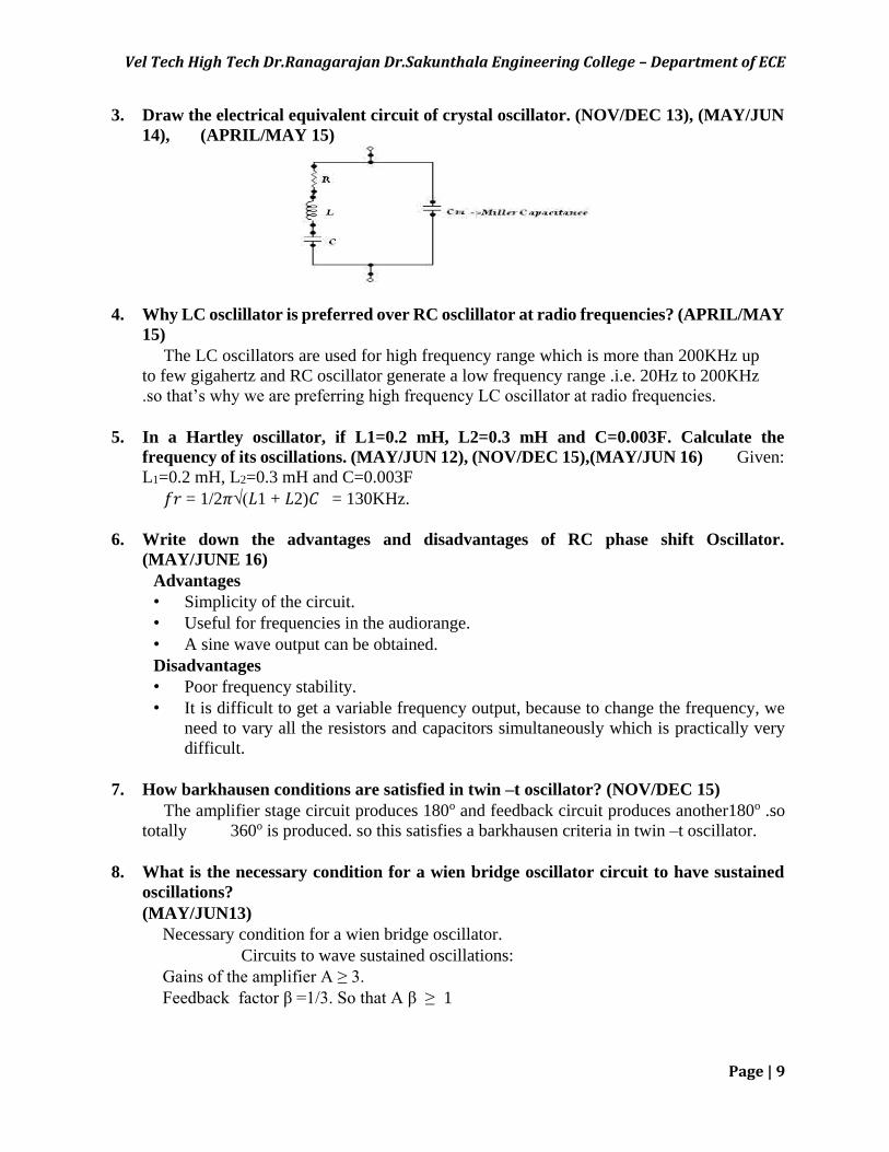
3. Draw the electrical equivalent circuit of crystal oscillator. (NOV/DEC 13), (MAY/JUN
14), (APRIL/MAY 15)
4. Why LC osclillator is preferred over RC osclillator at radio frequencies? (APRIL/MAY
15)
The LC oscillators are used for high frequency range which is more than 200KHz up
to few gigahertz and RC oscillator generate a low frequency range .i.e. 20Hz to 200KHz
.so that’s why we are preferring high frequency LC oscillator at radio frequencies.
5. In a Hartley oscillator, if L1=0.2 mH, L2=0.3 mH and C=0.003F. Calculate the
frequency of its oscillations. (MAY/JUN 12), (NOV/DEC 15),(MAY/JUN 16) Given:
L1=0.2 mH, L2=0.3 mH and C=0.003F
𝑓𝑟 = 1/2𝜋√(𝐿1 + 𝐿2)𝐶 = 130KHz.
6. Write down the advantages and disadvantages of RC phase shift Oscillator.
(MAY/JUNE 16)
Advantages
• Simplicity of the circuit.
• Useful for frequencies in the audiorange.
• A sine wave output can be obtained.
Disadvantages
• Poor frequency stability.
• It is difficult to get a variable frequency output, because to change the frequency, we
need to vary all the resistors and capacitors simultaneously which is practically very
difficult.
7. How barkhausen conditions are satisfied in twin –t oscillator? (NOV/DEC 15)
The amplifier stage circuit produces 180o and feedback circuit produces another180o .so
totally 360o is produced. so this satisfies a barkhausen criteria in twin –t oscillator.
8. What is the necessary condition for a wien bridge oscillator circuit to have sustained
oscillations?
(MAY/JUN13)
Necessary condition for a wien bridge oscillator.
Circuits to wave sustained oscillations:
Gains of the amplifier A ≥ 3.
Feedback factor β =1/3. So that A β ≥ 1
Vel Tech High Tech Dr.Ranagarajan Dr.Sakunthala Engineering College – Department of ECE
Page | 10
9. State Barkhausen criterion. (MAY/JUNE 15) (MAY/JUNE 17)
• The total phase shift around a loop, as the signal proceeds from input through amplifier,
feedback network back to input again, completing a loop, is precisely 00 or 3600.
• The magnitude of the product of the open loop gain of the amplifier (A) and the feedback
factor β is unity. i.e., A β = 1.
10. Comparison RC phase shift and wien bridge oscillator. (NOV/DEC 15)
S.No Parameter RC Phase shift oscillator Wein bridge oscillator
1. Feedback network Consists of three identical RC
sections connected in cascade
Uses wien bridge circuit
as feedback network
2. Phase shift introduced by
the feedback network 1800 at frequency of
oscillations
00 at frequency of
oscillations
6. minimum value of gain A>29 for sustained
oscillations
A> 3 for sustained
oscillations
11. Differentiate oscillator and amplifier. (NOV/DEC 13)
Oscillator Amplifier
1. They are self generating circuits that
generate waveforms like sine, square,
triangular of their own, without any input
signal.
1. They are not self generating circuits. These
circuits increase the level of the input signal that
is applied.
2.It has infinite gain 2.It has finite gain
3.It employs positive feedback 3.It employs negative feedback
12. A quartz crystal has L=3H, CS=0.05PF, R=2000Ω and CM=10pf. Calculate the series
and parallel resonant frequencies fs and fp of the crystal.(Nov 11)
FS=401.93Khz FP=411.96kHz
13. What is frequency stability of an oscillator? (May 10, Dec 13)
The measure of ability of an oscillator is to maintain the desired frequency as precisely
as possible for as long as time as possible.
14. Write down the advantages, disadvantages and applications of Hartley oscillator.
Advantages:
• It is easy to tune
• It can operate over a wide frequency typically from few Hz and several MHz. It is
easy to change the frequency by means of a variable capacitor.
Disadvantages:
• Poor frequency stability Applications:
• it is used as local oscillator in radio and TV receivers.
• In the function generator.
• In RF sources
Vel Tech High Tech Dr.Ranagarajan Dr.Sakunthala Engineering College – Department of ECE
Page | 11
PART B
1. Sketch the block diagram of a feedback amplifier and derive the expressions for gain
with positive and negative feedback. (APR 2011)
Refer:. S.Salivahanan ,N.Suresh Kumar,A.Vallavaraj, “Electronic Devices and
Circuits”;Page No.:423
2. Briefly explain the Barkhausen criterion for oscillation in feedback oscillator. (NOV
2013)
Refer:. S.Salivahanan ,N.Suresh Kumar,A.Vallavaraj, “Electronic Devices and
Circuits”;Page No.:424
3. Describe the principles involved in the Twin-T network, hence explain Twin –T
oscillator.
(APR 2016,NOV 2016)
Refer:. S.Salivahanan ,N.Suresh Kumar,A.Vallavaraj, “Electronic Devices and
Circuits”;Page No.:436
4. Explain frequency stability of feedback amplifiers.(APR 2016,NOV 2013)
Refer:. S.Salivahanan ,N.Suresh Kumar,A.Vallavaraj, “Electronic Devices and
Circuits”;Page No.:439
5. Explain RC phase shift oscillator with neat circuit diagram. Derive its frequency of
oscillation. Give the amplifier gain and feedback network gain to sustain oscillator
operation.(NOV 2013,14) Refer:. S.Salivahanan ,N.Suresh Kumar,A.Vallavaraj,
“Electronic Devices and Circuits”;Page No.:433
6. With the help of circuit diagram, Explain the principle of operation of a Colpitt’s
oscillator. Obtain the equation for the frequency of operation of the circuit. (NOV
2016,14)
Refer:. S.Salivahanan ,N.Suresh Kumar,A.Vallavaraj, “Electronic Devices and
Circuits”;Page No.:429
7. Draw the circuit diagram and explain the working of Hartley oscillator. Also derive
the expression for frequency of oscillation and condition for sustained
oscillations.(NOV 2016,13)
Refer:.S.Salivahanan ,N.Suresh Kumar,A.Vallavaraj, “Electronic Devices and
Circuits”;Page No.:427
8. With the help of circuit diagram, explain Barkhausen conditions are satisfied in wien
bridge oscillator using BJT.(NOV 2012)
Refer:. S.Salivahanan ,N.Suresh Kumar,A.Vallavaraj, “Electronic Devices and
Circuits”;Page No.:436
Vel Tech High Tech Dr.Ranagarajan Dr.Sakunthala Engineering College – Department of ECE
Page | 12
9. Briefly discuss about the frequency of oscillation of Franklin oscillator. (NOV 2016)
Refer:. S.Salivahanan ,N.Suresh Kumar,A.Vallavaraj, “Electronic Devices and
Circuits”;Page No.:431
10. Draw the circuit of tuned collector oscillator and state expression for its frequency.
(APR 2012)
Refer:. S.Salivahanan ,N.Suresh Kumar,A.Vallavaraj, “Electronic Devices and
Circuits”;Page No.:431
11. What is the principle of oscillation of crystals? Sketch the equivalent circuit and
impedancefrequency graph of crystals and obtain its series and parallel resonant
frequency. (NOV 2013,16) Refer:. S.Salivahanan ,N.Suresh Kumar,A.Vallavaraj,
“Electronic Devices and Circuits”;Page No.:437
12. In a Colpitts oscillator, the values of the inductors and capacitors in the tank circuit
are L=40Mh,C1=100pf,C2=500pf. Find Frequency of oscillation.(APR 2011)
1. If the output voltage is 10v, find the feedback voltage.
2. Find the minimum gain, if the frequency is changed by changing ‘L’ alone.
3. Find the value of C1 for a gain of 10.
Also, find the new frequency of oscillation.
Refer:. S.Salivahanan ,N.Suresh Kumar,A.Vallavaraj, “Electronic Devices and
Circuits”;Page No.:429
13. With a neat diagram, explain the operation of a transistor pierce and miller crystal
oscillator
(NOV 2014)(APR 2012,11)
Refer:. S.Salivahanan ,N.Suresh Kumar,A.Vallavaraj, “Electronic Devices and
Circuits”;Page No.:437
14. Calculate the frequency of oscillation for the clap oscillator with c1=0.1μf,c2=1μf,
C3=100pf and L=470μh. (NOV 2011)
Refer:. S.Salivahanan ,N.Suresh Kumar,A.Vallavaraj, “Electronic Devices and
Circuits”;Page No.:431
15. In a RC Phase shift oscillator, if R1=R2=R3=200K and C1=C2=C3=100PF, Find the
frequency of the oscillator. (APR 2013)
Refer:. S.Salivahanan ,N.Suresh Kumar,A.Vallavaraj, “Electronic Devices and
Circuits”;Page No.:433
Vel Tech High Tech Dr.Ranagarajan Dr.Sakunthala Engineering College – Department of ECE
Page | 13
UNIT-III TUNED AMPLIFIERS
PART A
1. What is the effect of Q on the resonance circuit? (MAY/JUNE 16)
• Bandwidth
• General spurious signal
• Oscillator phase noise
• Wide bandwidth
2. What are the different of coil losses? (MAY/JUN 16)
• Copper loss
• Eddy current loss
• Hysteresis loss
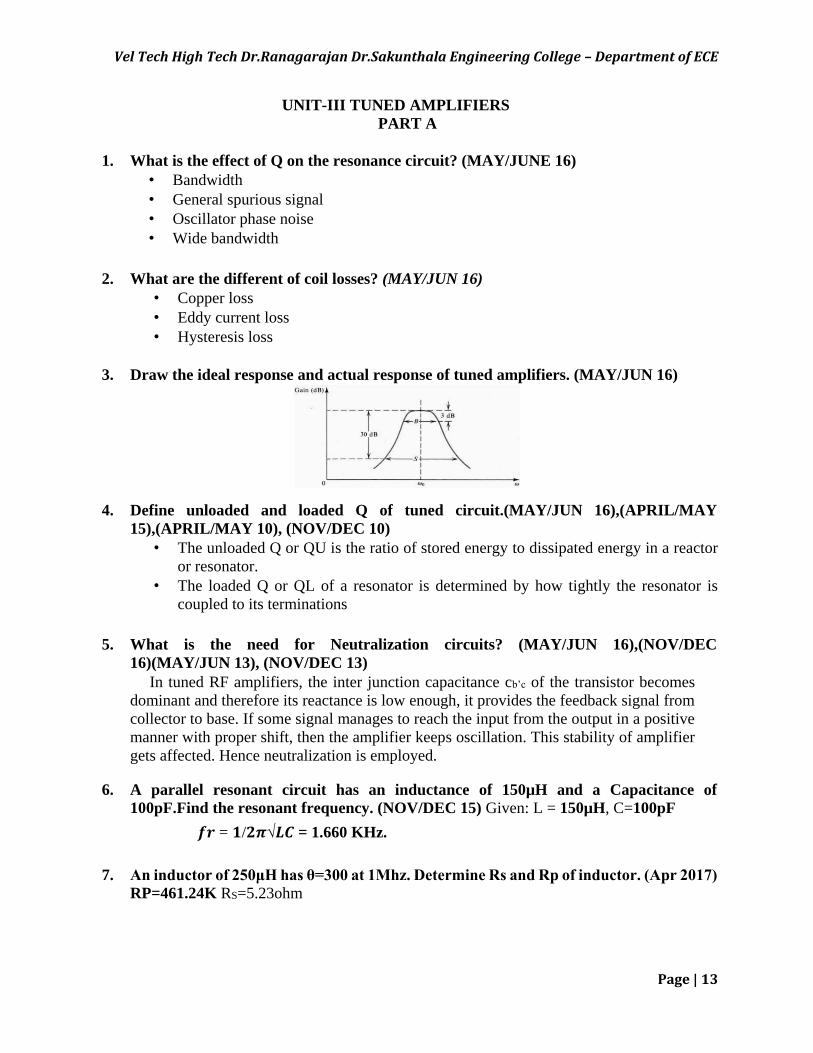
3. Draw the ideal response and actual response of tuned amplifiers. (MAY/JUN 16)
4. Define unloaded and loaded Q of tuned circuit.(MAY/JUN 16),(APRIL/MAY
15),(APRIL/MAY 10), (NOV/DEC 10)
• The unloaded Q or QU is the ratio of stored energy to dissipated energy in a reactor
or resonator.
• The loaded Q or QL of a resonator is determined by how tightly the resonator is
coupled to its terminations
5. What is the need for Neutralization circuits? (MAY/JUN 16),(NOV/DEC
16)(MAY/JUN 13), (NOV/DEC 13)
In tuned RF amplifiers, the inter junction capacitance cb’c of the transistor becomes
dominant and therefore its reactance is low enough, it provides the feedback signal from
collector to base. If some signal manages to reach the input from the output in a positive
manner with proper shift, then the amplifier keeps oscillation. This stability of amplifier
gets affected. Hence neutralization is employed.
6. A parallel resonant circuit has an inductance of 150µH and a Capacitance of
100pF.Find the resonant frequency. (NOV/DEC 15) Given: L = 150µH, C=100pF
𝒇𝒓 = 𝟏/𝟐𝝅√𝑳𝑪 = 1.660 KHz.
7. An inductor of 250μH has θ=300 at 1Mhz. Determine Rs and Rp of inductor. (Apr 2017)
RP=461.24K RS=5.23ohm
Vel Tech High Tech Dr.Ranagarajan Dr.Sakunthala Engineering College – Department of ECE
Page | 14
8. What is narrow band neutralization? (MAY/JUN 15), (NOV/DEC 14), (MAY/JUN 14),
(NOV/DEC 13), (APRIL/MAY 11).
The effect of collector to base capacitance of the transistor is neutralized by
introducing a signal that cancels the signal coupled through collector base capacitance. This
process is called neutralization
9. What is or what do you mean by a tuned amplifier? (NOV/DEC 13), (APRIL/MAY 10)
The amplifier with a circuit that is capable of amplifying a signal over a narrow
band of frequencies are called tuned amplifiers tuned amplifiers or The amplifiers which
amplify only selected range of frequencies (narrow band of frequencies) with the help of
tuned circuits (parallel LC circuit) are called tuned amplifiers.
10. What is a stagger tuned amplifier? What the advantages are of stagger tuned amplifier?
(NOV/DEC 14). (MAY/JUN 13),(NOV/DEC 11)
It is a circuit in which two single tuned cascaded amplifiers having certain
bandwidth are taken and their resonant frequencies are adjusted that they are separated
by an amount equal to the bandwidth of each stage. Since resonant frequencies are
displaced it is called stagger tuned amplifier .The advantage of stagger tuned amplifier is
to have better flat, wideband characteristics.
11. What is the effect of cascading n stages of identical stages of identical stages tuned
amplifiers (synchronously tuned) on the overall 3dB bandwidth? (APRIL/MAY 11)
BWn=BW (21/n-1)2. Where n-no. of stages.
Overall BW decreases as no. of stages decreases.
12. A tuned circuit has resonant frequency of 1600 KHz and bandwidth of 10KHz.What is
the value of its Q-factor? (MAY/JUN 12)
Q=fr/BW
=1600 KHz/10KHz=160.
13. What are the various types of tuned amplifiers? (NOV/DEC 13).
1) Small signal tuned amplifiers
a. Single tuned amplifiers
(i) Capacitive coupled
(ii) Inductively coupled (or)
Transformer coupled b.
Double tuned amplifiers
c. Stagger tuned amplifiers
2) Large signal tuned amplifiers
14. Mention the applications of class C tuned amplifier.(May-2015)
• Class C amplifiers are used primarily in high-power, high-frequency applications such as
Radiofrequency transmitters.
Vel Tech High Tech Dr.Ranagarajan Dr.Sakunthala Engineering College – Department of ECE
Page | 15
• In these applications, the high frequency pulses handled by the amplifier are not
themselves the signal, but constitute what is called the Carrier for the signal.
• Amplitude modulation is one such example.
• The principal advantage of class-C amplifier is that it has a higher efficiency than the other
amplifiers
PART B
1. Explain the working and frequency response of a capacitive coupled single tuned
amplifier circuit. (NOV 2017)(APR 2016,15)
Refer:. S.Salivahanan ,N.Suresh Kumar,A.Vallavaraj, “Electronic Devices and
Circuits”;Page No.:455
2. Describe briefly about neutralization in tuned amplifiers and explain in detail. (NOV
2017)(APR 2016,15)
Refer:. S.Salivahanan ,N.Suresh Kumar,A.Vallavaraj, “Electronic Devices and
Circuits”;Page No.:482
3. Draw the Double tuned amplifier and explain the frequency response. Derive the
expression for its gain and Bandwidth. (NOV 2012,10)
Refer:. S.Salivahanan ,N.Suresh Kumar,A.Vallavaraj, “Electronic Devices and
Circuits”;Page No.:433
4. Discuss the effect of cascading single tuned and double tuned amplifier on
bandwidth.(NOV
2016)
Refer:. S.Salivahanan ,N.Suresh Kumar,A.Vallavaraj, “Electronic Devices and
Circuits”;Page No.:473
5. With neat diagram, explain Stagger tuned amplifier. (NOV 2017)(APR 2015) Refer:.
S.Salivahanan ,N.Suresh Kumar,A.Vallavaraj, “Electronic Devices and Circuits”;Page
No.:475
6. Draw the circuit of Class C tuned amplifier and explain its operation with relevant
waveforms.
(N0V 2016)(APR 2015)
Refer:. S.Salivahanan ,N.Suresh Kumar,A.Vallavaraj, “Electronic Devices and
Circuits”;Page No.:477
7. A single tuned transistor amplifier is used to amplify modulated RF carrier of 600kHz
and bandwidth of 15kHz. The circuit has a total output resistance Rt=20k and output
capacitance Co=50Pf. Calculate value of inductance and capacitance of the tuned
circuit.(APR 2011)
Vel Tech High Tech Dr.Ranagarajan Dr.Sakunthala Engineering College – Department of ECE
Page | 16
Refer:. S.Salivahanan ,N.Suresh Kumar,A.Vallavaraj, “Electronic Devices and
Circuits”;Page No.:455
.
8. Discuss about hazeltine and coil neutralization in detail. .(NOV 2016)
Refer:. S.Salivahanan ,N.Suresh Kumar,A.Vallavaraj, “Electronic Devices and
Circuits”;Page No.:482
9. Explain the following: (NOV 2017)
1.Synchronously tuned amplifier 2. Stagger tuned amplifier
Refer:. S.Salivahanan ,N.Suresh Kumar,A.Vallavaraj, “Electronic Devices and
Circuits”;Page No.:475
10. Comparison between Tuned amplifier circuits.
Refer:. S.Salivahanan ,N.Suresh Kumar,A.Vallavaraj, “Electronic Devices and
Circuits”;Page No.:451
11. Consider the design of an IF amplifier for FM radio receiver. Using two synchronously
tuned stages with f0=10.7MHz and 3-dB bandwidth of each stage so that the overall
bandwidth is 200kHz. Using 3µH inductors find C and R for each stage.(APR 2015)
Refer:. S.Salivahanan ,N.Suresh Kumar,A.Vallavaraj, “Electronic Devices and
Circuits”;Page No.:455
UNIT-IV WAVE SHAPING AND MULTIVIBRATOR CIRCUITS
PART A
1. Why do we call astable multivibrator as free running multivibrator? (NOV/DEC 12)
Astable multivibrator is called as free running multivibrator because it generates square
wave without any triggering pulse.
2. Differentiate between clipper and clamper circuits. (APRIL/MAY 15)(NOV 2017)
Clipper Clamper
The circuits which are used to clip off the
unwanted portion of the waveform, without
distorting the remaining part of the waveform
The circuits which are used to add a dc level as
per the requirements to the ac output signal
Applications like TV, FM receivers. Applications like Radar, sonar system
3. State the role of commutating capacitors in bi-stable multivibrator. (MAY/JUN 16),
(APRIL/MAY 15)
The switching characteristics can be improved by passing the high frequency
components of the pulses. For this purpose, small capacitances are used in shunt with the
coupling resistors R1.Due to this, the transition time reduces considerably without affecting
the stable states. The capacitors allow fast rise and fall times. Thus it avoids any distortion in
the output waveform. as these capacitors help the multivibrator in making instantaneous
transitions between the states, they are known as commutating capacitors, speed-up capacitors
or transpose capacitors.
Vel Tech High Tech Dr.Ranagarajan Dr.Sakunthala Engineering College – Department of ECE
Page | 17
4. A RC low pass circuit has R=1.5KΩ and C=0.2µF.What is the rise rime of the output
when excited by a step input. (MAY/JUN 13),(MAY/JUN 16) Given: R=1.5KΩ and
C=0.2µF;
Rise time (tr) = 2.2 RC
= 2.2*1.5K*0.2µ=6.6*10-4s
5. Define the threshold points in a Schmitt trigger circuit. (NOV/DEC 13),(MAY/JUNE
16)
Schmitt trigger is a type of comparator with two different threshold voltage levels on
points (UTP or LTP).whenever the input signal goes over the high threshold levels, the output
of the comparator is switched high. The output will remain in the same state as long as the
input voltage is above the low threshold level. When the input voltage goes below this level,
the output will switch. These threshold voltage levels are called threshold points.
6. What are the different methods of generating ramp waveforms? (MAY/JUNE 16)
• Exponential charging
• Constant current charging
• Miller integration
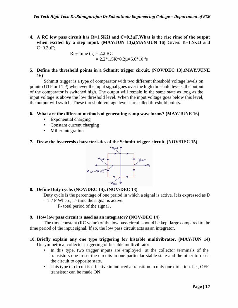
7. Draw the hysteresis characteristics of the Schmitt trigger circuit. (NOV/DEC 15)
8. Define Duty cycle. (NOV/DEC 14), (NOV/DEC 13)
Duty cycle is the percentage of one period in which a signal is active. It is expressed as D
= T / P Where, T- time the signal is active.
P- total period of the signal .
9. How low pass circuit is used as an integrator? (NOV/DEC 14)
The time constant (RC value) of the low pass circuit should be kept large compared to the
time period of the input signal. If so, the low pass circuit acts as an integrator.
10. Briefly explain any one type triggering for bistable multivibrator. (MAY/JUN 14)
Unsymmetrical collector triggering of bistable multivibrator:
• In this type, two trigger inputs are employed at the collector terminals of the
transistors one to set the circuits in one particular stable state and the other to reset
the circuit to opposite state.
• This type of circuit is effective in induced a transition in only one direction. i.e., OFF
transistor can be made ON
Vel Tech High Tech Dr.Ranagarajan Dr.Sakunthala Engineering College – Department of ECE
Page | 18
11.What is a regenerative comparator? Give an example circuit. (MAY/JUN 13)
Regenerative comparator is a circuit input compares its input voltage to a threshold
voltage. The threshold voltage used depends on the output state such that a high output to the
lower threshold voltage and a low output selects the upper threshold voltage. A small amount
of the output voltage is effectively before being added to the input voltage before it is
compared to a fixed threshold. So it uses positive or regenerative feedback.
12.What is meant by clamper circuits? (MAY/JUN 12)
The circuits which are used to add a dc level as per the requirements to the ac output signal
are called clamper circuits.
13.Why is monostable multivibrator also called as delay circuit? (NOV/DEC 15)
A monostable multivibrator produces a pulse or a rectangular waveform. The time
between the transition from quasi stable state to stable state can be pre determined and hence
it can be used to introduce the time delays with the help of fast transition . hence it is also
called a time delay circuit.
14.What is Low pass RC circuit? Why it is called low-pass filter?
• A simple circuit consisting of a series resistor and a shunt capacitor is called Low pass
RC circuit.
• At very high frequencies the capacitor acts as a virtual short circuit and output falls to
zero. Hence this circuit is called low-pass filter
PART B
1. With a neat circuit diagram and necessary wave forms, explain bistable multivibrator
operation.(APR 2013,15)
Refer:. S.Salivahanan ,N.Suresh Kumar,A.Vallavaraj, “Electronic Devices and
Circuits”;Page No.:563
2. Draw the circuit of differentiator and explain the generation of narrow spike from
square wave. What are its applications? (APR 2016)
Refer:. S.Salivahanan ,N.Suresh Kumar,A.Vallavaraj, “Electronic Devices and
Circuits”;Page No.:543
3. With neat circuit diagram, discuss Schmitt Trigger operation in detail. Obtain the
expression for UTP and LTP. (N0V 2017)(APR 2016)
Refer:. S.Salivahanan ,N.Suresh Kumar,A.Vallavaraj, “Electronic Devices and
Circuits”;Page No.:576
4. Write short notes on: (APR 2016)
1.Clipper 2.Clamper
Refer:. S.Salivahanan ,N.Suresh Kumar,A.Vallavaraj, “Electronic Devices and
Circuits”;Page No.:553
Vel Tech High Tech Dr.Ranagarajan Dr.Sakunthala Engineering College – Department of ECE
Page | 19
5. Design a Schmitt trigger circuit for Vcc=10V, UTP=5V,LTP=3V. Assume hfe=100 and
Ic=1mA.(N0V 2012)(MAY 2013)
Refer:. S.Salivahanan ,N.Suresh Kumar,A.Vallavaraj, “Electronic Devices and
Circuits”;Page No.:576
6. Design a collector coupled astable multivibrator for the following specifications:
Output voltage 10V peak, Ic=1mA,hfe=100,ICBO=0,Output to a positive pulse, the
duration of which is 20µ sec, the time between the pulse to be 10µsec. (MAY 2016)
Refer:. S.Salivahanan ,N.Suresh Kumar,A.Vallavaraj, “Electronic Devices and
Circuits”;Page No.:563
7. Draw the circuit of a collector coupled astable Multivibrator. Explain its operation and
mention the disadvantages of the circuit. (N0V 2017)
Refer:. S.Salivahanan ,N.Suresh Kumar,A.Vallavaraj, “Electronic Devices and
Circuits”;Page No.:563
8. Explain transistor switching time in detail. (APR 2011,13)
Refer:. S.Salivahanan ,N.Suresh Kumar,A.Vallavaraj, “Electronic Devices and
Circuits”;Page No.:563
9. Write short note on diode comparator and speed up capacitor. (NOV 2012)(APR 2013)
Refer:. S.Salivahanan ,N.Suresh Kumar,A.Vallavaraj, “Electronic Devices and
Circuits”;Page No.:552
10. Discuss about the working principle of Monostable oscillator with neat diagram.(APR
2016)
Refer:. S.Salivahanan ,N.Suresh Kumar,A.Vallavaraj, “Electronic Devices and
Circuits”;Page No.:563
11. Discuss the working of triggering of Bistable Multivibrator. (NOV 2011,14)
Refer:. S.Salivahanan ,N.Suresh Kumar,A.Vallavaraj, “Electronic Devices and
Circuits”;Page No.:563
12. Design a monostable multivibrator for the following specifications: Ic=1mA, hfe=100,
ICBO=0, Vcc=10V, VBB=6V,VBE=-0.5V, the duration of the output pulse=14msec.
Refer:. S.Salivahanan ,N.Suresh Kumar,A.Vallavaraj, “Electronic Devices and
Circuits”;Page No.:563
13. Design an astable multivibrator circuit to generate a 1kHz square wave. The supply
voltage is
5V and collector current is to be 2mA(Assume hfe=70) .(NOV 2013)
Refer:. S.Salivahanan ,N.Suresh Kumar,A.Vallavaraj, “Electronic Devices and
Circuits”;Page No.:563
Vel Tech High Tech Dr.Ranagarajan Dr.Sakunthala Engineering College – Department of ECE
Page | 20
UNIT-V BLOCKING OSCILLATORS AND TIMEBASE GENERATORS
PART A
1. Define slope error and displacement error. (MAY/JUN 16), (MAY/ JUNE 13)
Slope error: it is defined as differential in slope at beginning and end of sweep to
initial value of slope.
Displacement error: It is the maximum difference between the actual sweep
voltage and linear sweep voltage which passes through the beginning and end points of
actual sweep voltage.
2. Mention any two applications of blocking Oscillator. (MAY/JUN 16), (MAY/ JUNE
13), (APRIL/MAY11), (APRIL/MAY10), (NOV/DEC 10)
It is used in frequency dividers, low impedance switch, counter circuits and for
switching the other circuits.
3. List the characteristics of pulse transformer. (NOV/DEC 15)
• Generally ion cored and small in size
• The leakage inductance is minimum • The inter winding capacitance is low
• The cores have high permeability.
4. Name the different methods of generating a time base waveform.(APR/MAY 15)
• Voltage time base generator
• Current time base generator.
5. Mention the applications of voltage and current time base generator.(NOV/DEC 15)
• Used in deflection circuits in CRO
• In Radar and Television circuits
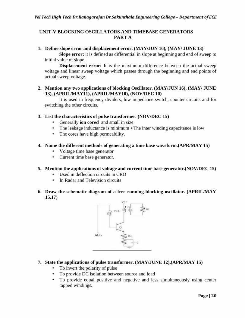
6. Draw the schematic diagram of a free running blocking oscillator. (APRIL/MAY
15,17)
7. State the applications of pulse transformer. (MAY/JUNE 12),(APR/MAY 15)
• To invert the polarity of pulse
• To provide DC isolation between source and load
• To provide equal positive and negative and less simultaneously using center
tapped windings.
Vel Tech High Tech Dr.Ranagarajan Dr.Sakunthala Engineering College – Department of ECE
Page | 21
8. State the limitation of low duty cycle in an astable blocking oscillator. (NOV/DEC
15)
• In low duty cycle operation, the voltage across the capacitor discharges very
slowly. due to this ,pulse at the collector has distorted waveform.
• The low duty cycle operation, also suffered from the problem of instability , due
to fluctuations in tf. This is due to the fact that after every cycle, the loop gain
does not change by the same amount and thus small change in v1 causes a large
change in tf.
9. What are restoration time and sweep time of a time base signal? (MAY/JUNE 12)
Restoration time: it is the time required for the return to initial value. It is also
called as return time or flyback time(Tr)
Sweep time: the period during which voltage increases linearly is called Sweep
time(Ts)
10. State any two methods of achieving sweep linearity of a time based waveform.
(NOV/DEC 12)
• Exponential charging
• Constant current charging
• Miller circuit
• Bootstrap circuit
11. What is the advantage of core saturation method of frequency control in a blocking
oscillator? (NOV/DEC 12)
The pulse duration depends on the supply voltage and the characteristics of core
and not the transistor parameters(hfe)
12. List the applications of time base generator.(NOV/DEC 13)
• Used in deflection circuits in CRO
• In Radar and Television circuits
13. Define Blocking Oscillator? (NOV/DEC 14)
A special type of wave generator which is used to produce a single narrow pulse or train
of pulses.
14. What is the function of time base circuit? (APRIL/MAY10)
A linear time base generator produces an output waveform which produces a
portion which exhibits a linear variation of voltage or current with respect to time.
Vel Tech High Tech Dr.Ranagarajan Dr.Sakunthala Engineering College – Department of ECE
Page | 22
PART B
1. With a neat circuit diagram and necessary wave forms, explain UJT operation.(NOV
2017,16)(APR 16)
Refer:. S.Salivahanan ,N.Suresh Kumar,A.Vallavaraj, “Electronic Devices and
Circuits”;Page No.:584
2. Draw the circuit of Astable blocking oscillator with base timing with neat
diagram.(N0V 2017,16) Refer:. S.Salivahanan ,N.Suresh Kumar,A.Vallavaraj,
“Electronic Devices and Circuits”;Page No.:598
3. With neat circuit diagram, discuss Miller time base circuit in detail. (NOV 2017)
Refer:. S.Salivahanan ,N.Suresh Kumar,A.Vallavaraj, “Electronic Devices and
Circuits”;Page No.:608
4. Write short notes on: .(NOV 2017)(APR 2016)
1.Current time base 2.Pulse transformer
Refer:. S.Salivahanan ,N.Suresh Kumar,A.Vallavaraj, “Electronic Devices and
Circuits”;Page No.:588
5. Explain Monostable blocking oscillator with emitter time in detail .(MAY 15)(NOV
14)
Refer:. S.Salivahanan ,N.Suresh Kumar,A.Vallavaraj, “Electronic Devices and
Circuits”;Page No.:603
6. With neat diagram, explain the bootstrap time base circuit operation. (NOV 12,14)
Refer:. S.Salivahanan ,N.Suresh Kumar,A.Vallavaraj, “Electronic Devices and
Circuits”;Page No.:608
7. Draw the circuit of free running blocking oscillator with neat diagram. Explain its
operation and mention the advantages and disadvantages of the circuit.(N0V
2017,16)
Refer:. S.Salivahanan ,N.Suresh Kumar,A.Vallavaraj, “Electronic Devices and
Circuits”;Page No.:598
8. Explain in detail voltage time base circuit operation. .(NOV 2017)
Refer:. S.Salivahanan ,N.Suresh Kumar,A.Vallavaraj, “Electronic Devices and
Circuits”;Page No.:608
Vel Tech High Tech Dr.Ranagarajan Dr.Sakunthala Engineering College – Department of ECE
Page | 23
Vel Tech High Tech Dr.Ranagarajan Dr.Sakunthala Engineering College – Department of ECE
Page | 24
Vel Tech High Tech Dr.Ranagarajan Dr.Sakunthala Engineering College – Department of ECE
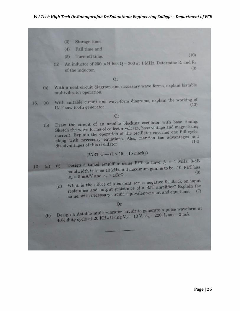
Page | 25
Vel Tech High Tech Dr.Ranagarajan Dr.Sakunthala Engineering College – Department of ECE
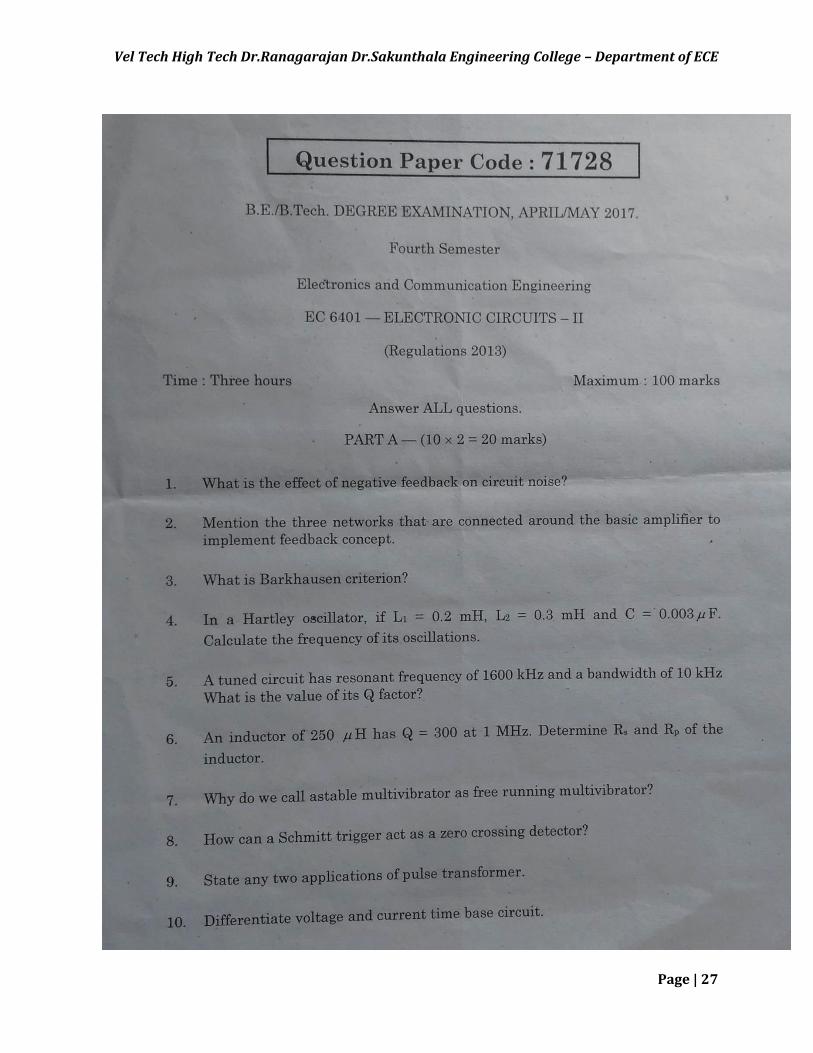
Page | 26
Vel Tech High Tech Dr.Ranagarajan Dr.Sakunthala Engineering College – Department of ECE
Page | 27
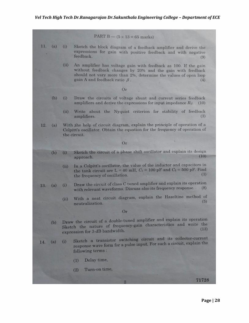
Vel Tech High Tech Dr.Ranagarajan Dr.Sakunthala Engineering College – Department of ECE
Page | 28
Vel Tech High Tech Dr.Ranagarajan Dr.Sakunthala Engineering College – Department of ECE
Page | 29