vel tech high tech dr.ranagarajan dr.sakunthala ... · vel tech high tech dr.ranagarajan...
TRANSCRIPT
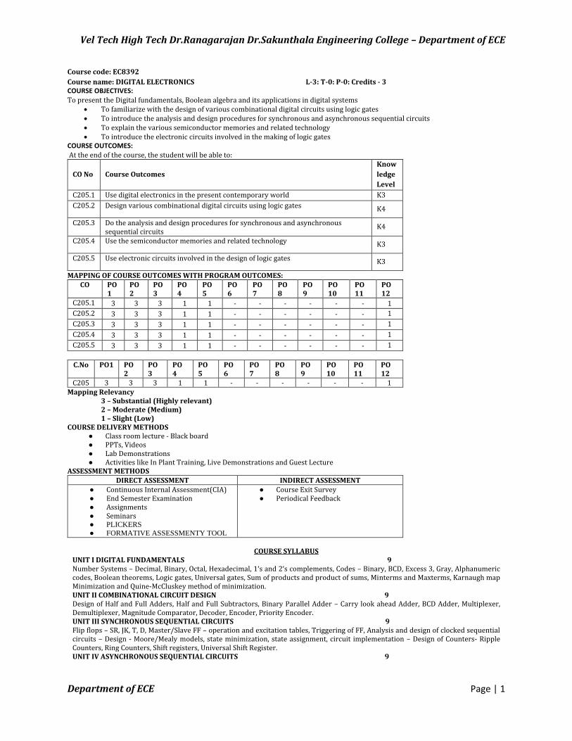
Vel Tech High Tech Dr.Ranagarajan Dr.Sakunthala Engineering College – Department of ECE
Department of ECE Page | 1
Course code: EC8392
Course name: DIGITAL ELECTRONICS L-3: T-0: P-0: Credits - 3 COURSE OBJECTIVES:
To present the Digital fundamentals, Boolean algebra and its applications in digital systems To familiarize with the design of various combinational digital circuits using logic gates To introduce the analysis and design procedures for synchronous and asynchronous sequential circuits To explain the various semiconductor memories and related technology To introduce the electronic circuits involved in the making of logic gates
COURSE OUTCOMES:
At the end of the course, the student will be able to:
CO No Course Outcomes
Know
ledge
Level
C205.1 Use digital electronics in the present contemporary world K3
C205.2 Design various combinational digital circuits using logic gates K4
C205.3 Do the analysis and design procedures for synchronous and asynchronous sequential circuits
K4
C205.4 Use the semiconductor memories and related technology K3
C205.5 Use electronic circuits involved in the design of logic gates K3
MAPPING OF COURSE OUTCOMES WITH PROGRAM OUTCOMES: CO PO
1 PO 2
PO 3
PO 4
PO 5
PO 6
PO 7
PO 8
PO 9
PO 10
PO 11
PO 12
C205.1 3 3 3 1 1 - - - - - - 1
C205.2 3 3 3 1 1 - - - - - - 1
C205.3 3 3 3 1 1 - - - - - - 1
C205.4 3 3 3 1 1 - - - - - - 1
C205.5 3 3 3 1 1 - - - - - - 1
C.No PO1 PO
2 PO 3
PO 4
PO 5
PO 6
PO 7
PO 8
PO 9
PO 10
PO 11
PO 12
C205 3 3 3 1 1 - - - - - - 1 Mapping Relevancy 3 – Substantial (Highly relevant) 2 – Moderate (Medium) 1 – Slight (Low) COURSE DELIVERY METHODS
● Class room lecture - Black board ● PPTs, Videos ● Lab Demonstrations ● Activities like In Plant Training, Live Demonstrations and Guest Lecture
ASSESSMENT METHODS DIRECT ASSESSMENT INDIRECT ASSESSMENT
● Continuous Internal Assessment(CIA) ● End Semester Examination ● Assignments ● Seminars ● PLICKERS
● FORMATIVE ASSESSMENTY TOOL
● Course Exit Survey ● Periodical Feedback
COURSE SYLLABUS
UNIT I DIGITAL FUNDAMENTALS 9 Number Systems – Decimal, Binary, Octal, Hexadecimal, 1‘s and 2‘s complements, Codes – Binary, BCD, Excess 3, Gray, Alphanumeric codes, Boolean theorems, Logic gates, Universal gates, Sum of products and product of sums, Minterms and Maxterms, Karnaugh map Minimization and Quine-McCluskey method of minimization. UNIT II COMBINATIONAL CIRCUIT DESIGN 9 Design of Half and Full Adders, Half and Full Subtractors, Binary Parallel Adder – Carry look ahead Adder, BCD Adder, Multiplexer, Demultiplexer, Magnitude Comparator, Decoder, Encoder, Priority Encoder. UNIT III SYNCHRONOUS SEQUENTIAL CIRCUITS 9 Flip flops – SR, JK, T, D, Master/Slave FF – operation and excitation tables, Triggering of FF, Analysis and design of clocked sequential circuits – Design - Moore/Mealy models, state minimization, state assignment, circuit implementation – Design of Counters- Ripple Counters, Ring Counters, Shift registers, Universal Shift Register. UNIT IV ASYNCHRONOUS SEQUENTIAL CIRCUITS 9
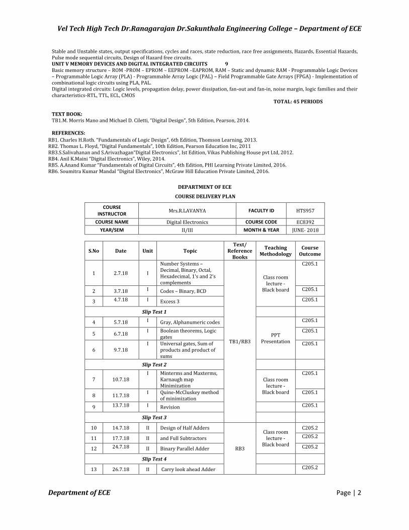
Vel Tech High Tech Dr.Ranagarajan Dr.Sakunthala Engineering College – Department of ECE
Department of ECE Page | 2
Stable and Unstable states, output specifications, cycles and races, state reduction, race free assignments, Hazards, Essential Hazards, Pulse mode sequential circuits, Design of Hazard free circuits. UNIT V MEMORY DEVICES AND DIGITAL INTEGRATED CIRCUITS 9 Basic memory structure – ROM -PROM – EPROM – EEPROM –EAPROM, RAM – Static and dynamic RAM - Programmable Logic Devices – Programmable Logic Array (PLA) - Programmable Array Logic (PAL) – Field Programmable Gate Arrays (FPGA) - Implementation of combinational logic circuits using PLA, PAL. Digital integrated circuits: Logic levels, propagation delay, power dissipation, fan-out and fan-in, noise margin, logic families and their characteristics-RTL, TTL, ECL, CMOS
TOTAL: 45 PERIODS
TEXT BOOK: TB1.M. Morris Mano and Michael D. Ciletti, “Digital Design”, 5th Edition, Pearson, 2014. REFERENCES:
RB1. Charles H.Roth. “Fundamentals of Logic Design”, 6th Edition, Thomson Learning, 2013. RB2. Thomas L. Floyd, “Digital Fundamentals”, 10th Edition, Pearson Education Inc, 2011 RB3.S.Salivahanan and S.Arivazhagan“Digital Electronics”, Ist Edition, Vikas Publishing House pvt Ltd, 2012. RB4. Anil K.Maini “Digital Electronics”, Wiley, 2014. RB5. A.Anand Kumar “Fundamentals of Digital Circuits”, 4th Edition, PHI Learning Private Limited, 2016. RB6. Soumitra Kumar Mandal “Digital Electronics”, McGraw Hill Education Private Limited, 2016.
DEPARTMENT OF ECE
COURSE DELIVERY PLAN
COURSE
INSTRUCTOR Mrs.R.LAVANYA FACULTY ID HTS957
COURSE NAME Digital Electronics COURSE CODE EC8392
YEAR/SEM II/III MONTH & YEAR JUNE- 2018
S.No Date Unit Topic Text/
Reference Books
Teaching Methodology
Course Outcome
1 2.7.18 I
Number Systems – Decimal, Binary, Octal, Hexadecimal, 1‘s and 2‘s complements
TB1/RB3
Class room lecture -
Black board
C205.1
2 3.7.18 I Codes – Binary, BCD C205.1
3 4.7.18 I Excess 3 C205.1
Slip Test 1
4 5.7.18 I Gray, Alphanumeric codes
PPT Presentation
C205.1
5 6.7.18 I Boolean theorems, Logic
gates C205.1
6 9.7.18 I Universal gates, Sum of
products and product of sums
C205.1
Slip Test 2
7 10.7.18 I Minterms and Maxterms,
Karnaugh map Minimization
Class room lecture -
Black board
C205.1
8 11.7.18 I Quine-McCluskey method
of minimization C205.1
9 13.7.18 I Revision C205.1
Slip Test 3
10 14.7.18 II Design of Half Adders
RB3
Class room lecture -
Black board
C205.2
11 17.7.18 II and Full Subtractors C205.2
12 24.7.18 II Binary Parallel Adder C205.2
Slip Test 4
13 26.7.18 II Carry look ahead Adder C205.2
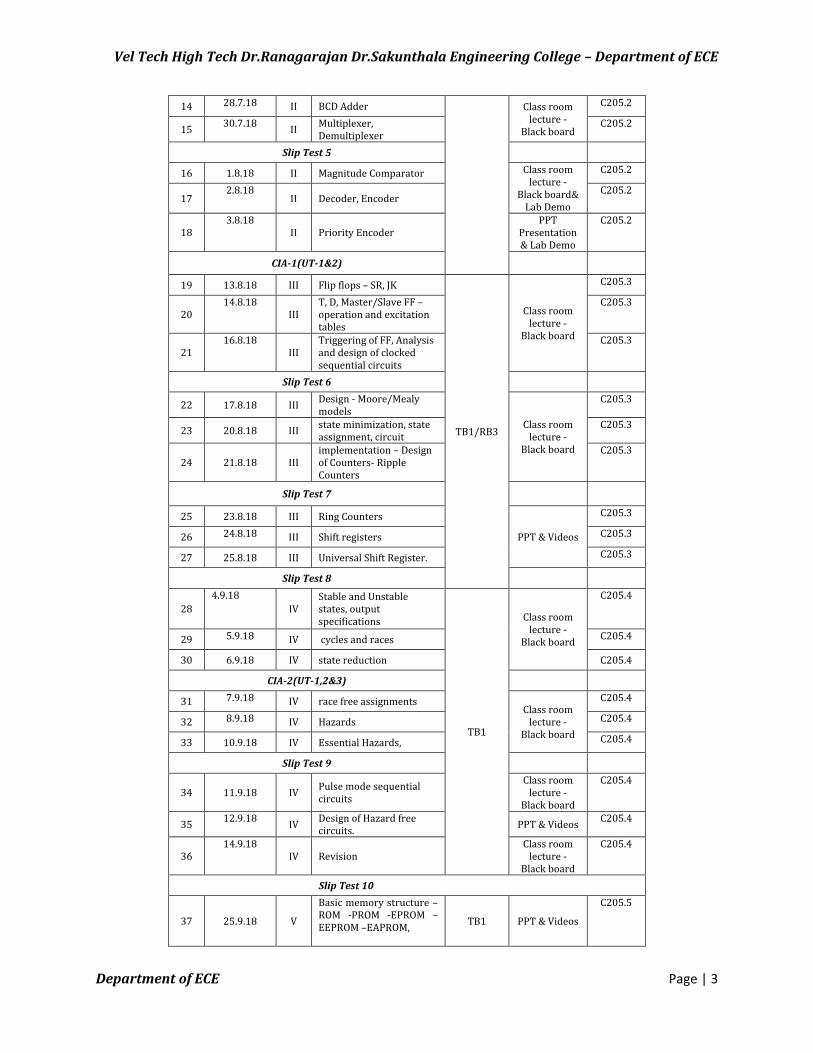
Vel Tech High Tech Dr.Ranagarajan Dr.Sakunthala Engineering College – Department of ECE
Department of ECE Page | 3
14 28.7.18 II BCD Adder Class room lecture -
Black board
C205.2
15 30.7.18
II Multiplexer, Demultiplexer
C205.2
Slip Test 5
16 1.8.18 II Magnitude Comparator Class room lecture -
Black board& Lab Demo
C205.2
17 2.8.18
II Decoder, Encoder C205.2
18 3.8.18
II Priority Encoder PPT
Presentation & Lab Demo
C205.2
CIA-1(UT-1&2)
19 13.8.18 III Flip flops – SR, JK
TB1/RB3
Class room lecture -
Black board
C205.3
20 14.8.18
III T, D, Master/Slave FF – operation and excitation tables
C205.3
21 16.8.18
III Triggering of FF, Analysis and design of clocked sequential circuits
C205.3
Slip Test 6
22 17.8.18 III Design - Moore/Mealy models
Class room lecture -
Black board
C205.3
23 20.8.18 III state minimization, state assignment, circuit
C205.3
24 21.8.18 III implementation – Design of Counters- Ripple Counters
C205.3
Slip Test 7
25 23.8.18 III Ring Counters
PPT & Videos
C205.3
26 24.8.18 III Shift registers C205.3
27 25.8.18 III Universal Shift Register. C205.3
Slip Test 8
28
4.9.18
IV Stable and Unstable states, output specifications
TB1
Class room lecture -
Black board
C205.4
29 5.9.18 IV cycles and races C205.4
30 6.9.18 IV state reduction C205.4
CIA-2(UT-1,2&3)
31 7.9.18 IV race free assignments Class room
lecture - Black board
C205.4
32 8.9.18 IV Hazards C205.4
33 10.9.18 IV Essential Hazards, C205.4
Slip Test 9
34 11.9.18 IV Pulse mode sequential circuits
Class room lecture -
Black board
C205.4
35 12.9.18
IV Design of Hazard free circuits.
PPT & Videos C205.4
36 14.9.18
IV Revision Class room
lecture - Black board
C205.4
Slip Test 10
37 25.9.18 V
Basic memory structure – ROM -PROM -EPROM – EEPROM –EAPROM,
TB1 PPT & Videos
C205.5
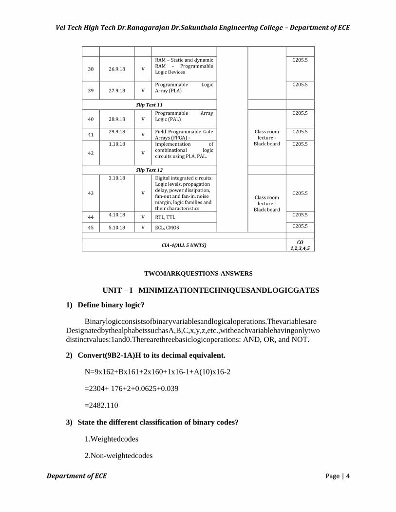
Vel Tech High Tech Dr.Ranagarajan Dr.Sakunthala Engineering College – Department of ECE
Department of ECE Page | 4
38 26.9.18 V
RAM – Static and dynamic RAM - Programmable Logic Devices
C205.5
39 27.9.18 V Programmable Logic Array (PLA)
C205.5
Slip Test 11
40 28.9.18 V Programmable Array Logic (PAL)
Class room lecture -
Black board
C205.5
41 29.9.18
V Field Programmable Gate Arrays (FPGA) -
C205.5
42
1.10.18
V
Implementation of combinational logic circuits using PLA, PAL.
C205.5
Slip Test 12
43
3.10.18
V
Digital integrated circuits: Logic levels, propagation delay, power dissipation, fan-out and fan-in, noise margin, logic families and their characteristics
Class room lecture -
Black board
C205.5
44 4.10.18 V RTL, TTL C205.5
45 5.10.18 V ECL, CMOS C205.5
CIA-4(ALL 5 UNITS) CO
1,2,3,4,5
TWOMARKQUESTIONS-ANSWERS
UNIT – I MINIMIZATIONTECHNIQUESANDLOGICGATES
1) Define binary logic?
Binarylogicconsistsofbinaryvariablesandlogicaloperations.Thevariablesare
DesignatedbythealphabetssuchasA,B,C,x,y,z,etc.,witheachvariablehavingonlytwo
distinctvalues:1and0.Therearethreebasiclogicoperations: AND, OR, and NOT.
2) Convert(9B2-1A)H to its decimal equivalent.
N=9x162+Bx161+2x160+1x16-1+A(10)x16-2
=2304+ 176+2+0.0625+0.039
=2482.110
3) State the different classification of binary codes?
1.Weightedcodes
2.Non-weightedcodes
Vel Tech High Tech Dr.Ranagarajan Dr.Sakunthala Engineering College – Department of ECE
Department of ECE Page | 5
3.Reflectivecodes
4.Sequentialcodes
5.Alphanumericcodes
6.ErrorDetectingandcorrectingcodes.
4)List the different number systems?
i)Decimal Number system
ii)Binary Number system
iii)Octal Number system
iv)Hexadecimal Number
system
5)Write the names of basic logical operators.
1.NOT/INVERT
2.AND
3.OR
6)What are basic properties of Boolean algebra?
ThebasicpropertiesofBooleanalgebraarecommutativeproperty,associative
Property and distributive property.
7)State the associative property of Boolean algebra.
TheassociativepropertyofBooleanalgebrastatesthattheORingofseveral
variablesresultsinthesameregardlessofthegroupingofthevariables.Theassociative
property is stated as follows:
A+(B+C)=(A+B)+C
8)State the commutative property of Boolean algebra.
ThecommutativepropertystatesthattheorderinwhichthevariablesareORedmakesnodiff
er ence.Thecommutativepropertyis:
A+B=B+A
9)State the distributive property of Boolean algebra.
ThedistributivepropertystatesthatANDingseveralvariablesandORingthe
resultWithasinglevariableisequivalenttoORingthesinglevariablewitheachofthe
Vel Tech High Tech Dr.Ranagarajan Dr.Sakunthala Engineering College – Department of ECE
Department of ECE Page | 6
theseveralVariablesandthenANDingthesums.Thedistributivepropertyis:
A+BC=(A+B)(A+C)
10)State the absorption law of Boolean algebra.
The absorption law of Boolean algebra is given by X+XY=X,X(X+Y)=X.
11)State DeMorgan's theorem.
DeMorgan suggested two theorems that form important part of Boolean algebra.
They are,
1)The complement of a product is equal to the sum of the complements.
(AB)'=A'+B'
2)The complement of a sum term is equal to the product of the complements.
(A+B)'=A'B'
12)Reduce A(A+B)
A(A+B)=AA+A
B
=A(1+B)[1+B=
1] =A.
13)Reduce A'B'C'+A'BC'+A'BC
A'B'C'+A'BC'+A'BC=A'C'(B'+B)+ A'B'C
=A'C'+A'BC[A+A'=1]
=A'(C'+BC)
=A'(C'+B)[A+A'B=A+B]
14)Reduce AB+(AC)'+AB’C(AB+C)
AB+(AC)'+AB‟C(AB+C)=AB+(AC)'+AAB'BC+AB'CC
=AB+(AC)'+AB'CC[A.A'= 0]
=AB+(AC)'+AB'C[A.A=1]
=AB+A'+ C'=AB'C[(AB)'=A'+B']
=A'+B+C'+AB'C[A+AB'=A+B]
=A'+B'C+B+C'[A+A'B=A+B]
=A'+B+C'+B'C
=A'+B+C'+B'
=A'+C'+1
=1[A+1=1]
Vel Tech High Tech Dr.Ranagarajan Dr.Sakunthala Engineering College – Department of ECE
Department of ECE Page | 7
15. Simplify the following expression Y=(A+B)(A+C’)(B'+C’) Y=(A+B)(A+
C‟)(B'+C‟)
=(AA'+AC+A'B+BC)(B'+C')[A.A'=0]
=(AC+ A'B+BC)(B'+C‟)
=AB'C+ACC'+A'BB'+A'BC'+ BB'C+ BCC'
=AB'C+A'BC'
16. Show that (X+Y'+XY)(X+Y')(X'Y)=0
(X+Y'+XY)(X+Y')(X'Y)=(X+Y'+X)(X+Y‟)(X'+Y)[A+A'B=A+B]
=(X+Y‟)(X+Y‟)(X'Y)[A+A=1]
=(X+Y‟)(X'Y)[A.A= 1]
=X.X'+Y'.X'.Y
=0[A.A'=0]
17. Prove that ABC+ABC'+AB'C+A'BC=AB+AC+BC
ABC+ABC'+ AB'C+A'BC=AB(C+C')+AB'C+A'BC
=AB+AB'C+A'BC
=A(B+B'C)+A'BC
=A(B+ C)+A'BC
=AB+AC+A'BC
=B(A+ C)+AC
=AB+BC+AC
=AB+AC+BC...Proved
18. Convert the given expression in canonical SOP form Y=AC+AB+ BC
Y=AC+AB+BC
=AC(B+B‟)+AB(C+C‟)+(A+A')BC
=ABC+ABC'+AB'C+AB'C'+ABC+ABC'+ABC
=ABC+ABC'+AB'C+AB'C'[A+ A=1]
19. Define duality property.
Dualitypropertystatesthateveryalgebraicexpressiondeduciblefromthe
postulatesOfBooleanalgebraremainsvalidiftheoperatorsandidentityelementsare
interchanged.Ifthedualofanalgebraicexpressionisdesired,wesimplyinterchangeORand
ANDoperatorsandreplace1'sby0'sand0'sby1's.
20.FindthecomplementofthefunctionsF1=x'yz'+x'y'zandF2=x(y'z'+yz). By applying
DeMorgan's theorem.
F1'=(x'yz'+x'y'z)'=(x'yz')'(x'y'z)'=(x+y'+ z)(x+y+z')
F2'=[x(y'z'+yz)]'=x'+(y'z'+yz)'
Vel Tech High Tech Dr.Ranagarajan Dr.Sakunthala Engineering College – Department of ECE
Department of ECE Page | 8
=x'+(y'z')'(yz)'
=x'+(y+z)(y'+z')
21 Simplify the following expression
Y=(A+B)(A=C)(B+C)
=(AA+AC+AB+BC)(B+C)
=(AC+AB+BC)(B+C)
=ABC+ ACC+ABB+ABC+BBC+ BCC
=ABC
22WhatarethemethodsadoptedtoreduceBooleanfunction?
i)Karnaugmap ii)TabularmethodorQuineMc-
Cluskeymethod iii)Variableenteredmaptechnique.
23)State the limitations of karnaugh map.
i)Generally it is limited to six variable map(i.e)more then six variable
involving expression are not reduced.
ii)The map method is restricted in its capability since they are useful for
simplifying only Boolean expression represented in standard form.
24)What are called don’t care conditions?
In some logic circuits certain input conditions never occur, therefore the
Corresponding output never appears. In such cases the output levelisnot
defined,itcanbeeitherhighorlow.Theseoutputlevelsareindicatedby„X‟or„d‟inthetruth
tables and are called don‟t care conditions orin completely specified functions.
25)What is a prime implicant?
A prime implicant is a product term obtained by combining the maximum
possible number of adjacent squares in the map.
26)What is an essential implicant?
If a minterm is covered by only one prime implicant, the prime implicant is
said to be essential
27.What is a Logic gate?
Logic gates are the basic elements that make up a digital system. The electronic gate
Is a circuit that is able to operate on a number of binary inputs in order to perform a
Particular logical function.
Vel Tech High Tech Dr.Ranagarajan Dr.Sakunthala Engineering College – Department of ECE
Department of ECE Page | 9
28.What is High Threshold Logic?
Some digital circuits operate in environments, which produce very high noise
signals. For operation in such surroundings there is available at type DTL gate which
Possesses a high threshold to noise immunity. This type of gate is called HTL logic or
High Threshold Logic.
29.WhatarethetypesofTTLlogic?
1.Opencollectoroutput
2.Totem-PoleOutput 3.Tri-
stateoutput.
30. What is depletion mode operation MOS?
Ifthechannelisinitiallydopedlightlywithp-typeimpurityaconductingchannel
existsatzerogatevoltageandthedeviceissaidtooperateindepletionmode.
31.What is enhancement mode operation of MOS?
Iftheregionbeneaththegateisleftinitiallyunchargedthegatefieldmust induce
achannelbeforecurrentcanflow.Thusthegatevoltageenhancesthechannelcurrent and
such a device is said to operate in the enhancement mode.
32.MentionthecharacteristicsofMOStransistor?
1.Then-channelMOSconductswhenitsgate-to-sourcevoltageispositive. 2.Thep-
channelMOSconductswhenitsgate-to-sourcevoltageisnegative
3.Eithertypeofdeviceisturnedofifitsgate-to-sourcevoltageiszero.
33.ListthedifferentversionsofTTL
1.TTL(Std.TTL)
2.LTTL(LowPowerTTL)
3.HTTL(HighSpeedTTL)
4.STTL(SchottkyTTL)
5.LSTTL(LowpowerSchottkyTTL)
34.Why totem pole outputs cannot be connected together.
Totem pole outputs cannot be connected together because such a connection
might produce excessive current and may resulting damage to the devices.
Vel Tech High Tech Dr.Ranagarajan Dr.Sakunthala Engineering College – Department of ECE
Department of ECE Page | 10
UNIT-IICOMBINATIONALCIRCUITS
1. Definecombinationallogic
When logic gates are connected together to produce a specified output for
certain Specified combinations of input variables ,with no storage involved, the
resulting circuit is Called combinational logic.
2.Explainthedesignprocedureforcombinationalcircuits
The problem definition Determine the number of available input variables & required
O/P variables. Assigning letter symbols to I/O variables
Obtain simplified Boolean expression for each O/P.
Obtain the logic diagram.
3.Define Half adder and full adder
The logic circuit that performs the addition of two bits is a half adder. The circuit
that Performs the addition of three bits is a full adder.
4. Define Decoder?
A decoder is a multiple-input multiple output logic circuit that converts
coded input sin to coded outputs where the input and output codes are different.
5. What is binary decoder?
A decoder is a combinational circuit that converts binary information from n
input lines to a maximum of 2n outputs lines.
6. Define Encoder?
An encoder has 2n input lines and n output lines. In encoder the output lines
generate The binary code corresponding to the input value.
7.WhatispriorityEncoder?
A priority encoder is an encoder circuit that includes the priority function. In
priority encoder, if 2 or more inputs are equal to 1at the same time, the input
having The highest Priority will take precedence.
8.Definemultiplexer?
Multiplexer is a digital switch .I fallows digital information from several sources
to be Routed on to a single output line.
9.What do you mean by comparator?
A comparator is a special combinational circuit designed primarily to compare the
Relative magnitude of two binary numbers.
Vel Tech High Tech Dr.Ranagarajan Dr.Sakunthala Engineering College – Department of ECE
Department of ECE Page | 11
10.Listbasictypesofprogrammablelogicdevices.
.Read only memory
.Programmable logic Array
.Programmable Array Logic
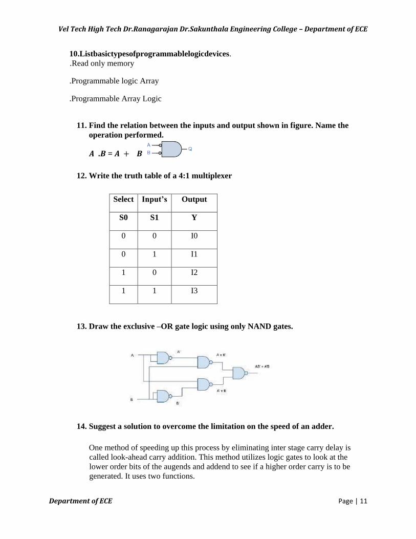
11. Find the relation between the inputs and output shown in figure. Name the
operation performed.
𝑨 .𝑩 = 𝑨 + 𝑩
12. Write the truth table of a 4:1 multiplexer
Select Input’s Output
S0 S1 Y
0 0 I0
0 1 I1
1 0 I2
1 1 I3
13. Draw the exclusive –OR gate logic using only NAND gates.
14. Suggest a solution to overcome the limitation on the speed of an adder.
One method of speeding up this process by eliminating inter stage carry delay is
called look-ahead carry addition. This method utilizes logic gates to look at the
lower order bits of the augends and addend to see if a higher order carry is to be
generated. It uses two functions.
Vel Tech High Tech Dr.Ranagarajan Dr.Sakunthala Engineering College – Department of ECE
Department of ECE Page | 12
Carry generate
Carry propagate
15. Differentiate a decoder from a demultiplexer.
S.No Decoder Demultiplexer
1. A decoder is a multiple input
multiple output logic circuit
with converts coded input
into coded outputs, where the
input and output codes are
different.
A demultiplexer is a circuit
that receivers information on
a single line and transmits
this information on one of 2n
possible output lines.
16. Write an expression for barrow and difference in a full subtractor circuits.
For Borrow: D=𝐴𝐵 Bin+𝐴 B𝐵 in +ABB in
For Difference: Bout= B in +𝐴𝐵+B B in
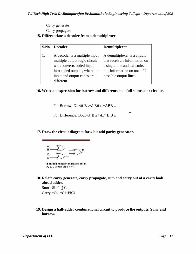
17. Draw the circuit diagram for 4 bit odd parity generator.
18. Relate carry generate, carry propagate, sum and carry out of a carry look
ahead adder.
Sum =Si=Pi Ci
Carry =Ci+1=Gi+PiCi
19. Design a half-adder combinational circuit to produce the outputs. Sum and
barrow.
Vel Tech High Tech Dr.Ranagarajan Dr.Sakunthala Engineering College – Department of ECE
Department of ECE Page | 13
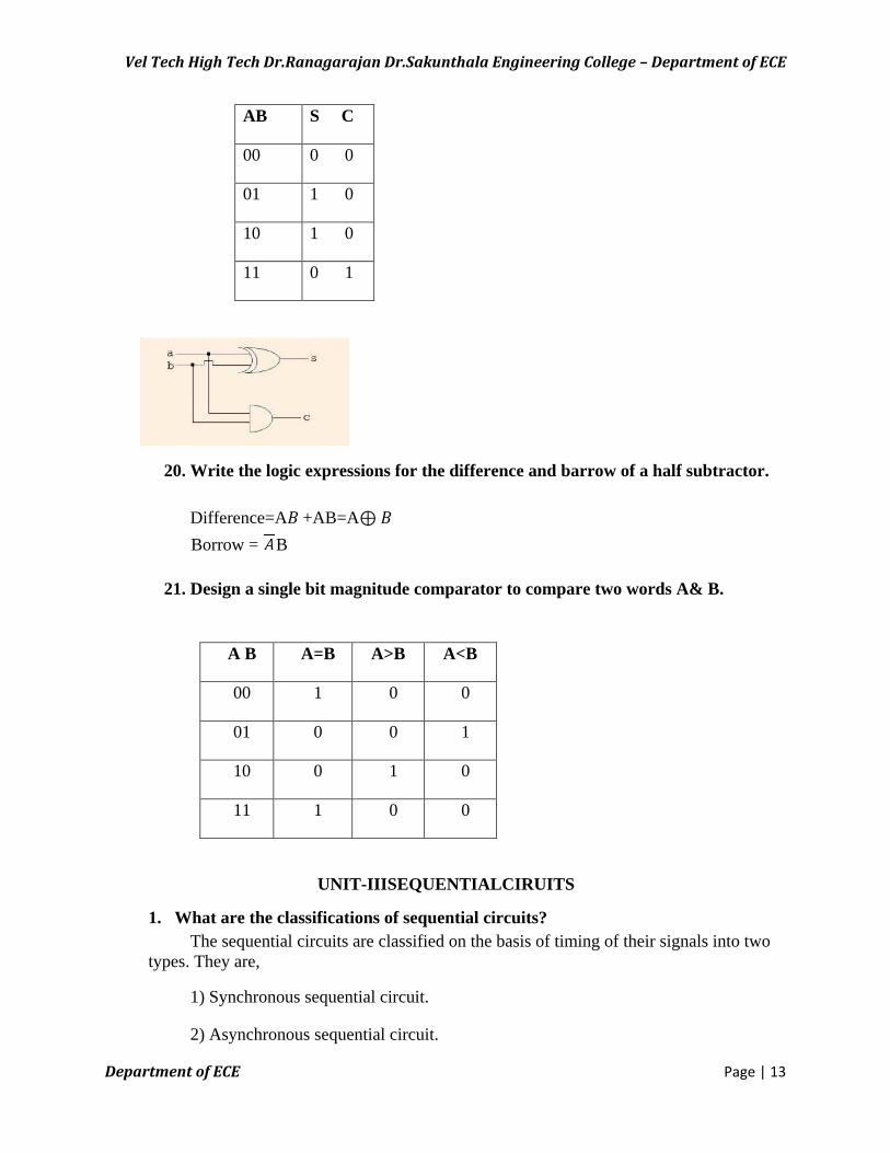
AB S C
00 0 0
01 1 0
10 1 0
11 0 1
20. Write the logic expressions for the difference and barrow of a half subtractor.
Difference=A𝐵 +AB=A⊕ 𝐵
Borrow = B
21. Design a single bit magnitude comparator to compare two words A& B.
A B A=B A>B A<B
00 1 0 0
01 0 0 1
10 0 1 0
11 1 0 0
UNIT-IIISEQUENTIALCIRUITS
1. What are the classifications of sequential circuits?
The sequential circuits are classified on the basis of timing of their signals into two
types. They are,
1) Synchronous sequential circuit.
2) Asynchronous sequential circuit.
Vel Tech High Tech Dr.Ranagarajan Dr.Sakunthala Engineering College – Department of ECE
Department of ECE Page | 14
2. Define Flip flop.
The basic unit for storage is flip flop. A flip-flop maintains its output state either
at1or0untildirectedbyaninputsignaltochangeitsstate.
3. What are the different types of flip-flop?
There are various types of flip flops. Some of them are mentioned below they
are, RS flip-flop
SR flip-flop
D flip-flop
JK flip-flop
T flip-flop
4. What is the operation of RS flip-flop?
When R input is low and S input is high the Q output of flip-flop is set.
When R input is high and S input is low the Q output of flip-flop is
reset. When both the inputs R and S are low the output does not
change When both the inputs R and S are high the output is
unpredictable.
5. What is the operation of SR flip-flop?
• When R input is low and S input is high the Q output of flip-flop is set.
• When R input is high and S input is low the Q output of flip-flop is reset.
• When both the inputs R and S are low the output does not change.
• When both the inputs R and S are high the output is unpredictable.
6. What is the operation of Dflip-flop?
InDflip-flopduringtheoccurrenceofclockpulseifD=1,theoutputQissetand if
D=0,theoutputisreset.
7.WhatistheoperationofJKflip-flop?
• When K input is low and J input is high the Q output of flip-
flop is set.
• When K input is high and J input is low the Q output of flip-
flop is reset.
• When both the inputs K and J are low the output does not
change
• When both the inputs K and J are high it is possible to set or
reset the flip-flop(ie) the output toggle on then extpositive
clock edge.
8.WhatistheoperationofTflip-flop?
T flip-flop is also known as Toggle flip-flop.
When T=0thereisnochangeintheoutput.
When T=1theoutputswitchtothecomplementstate(ie)the output toggles.
Vel Tech High Tech Dr.Ranagarajan Dr.Sakunthala Engineering College – Department of ECE
Department of ECE Page | 15
9. Define race around condition.
InJKflip-flopoutputisfedbacktotheinput.Thereforechangeintheoutput results
Change in the input. Due to this in the positive half of the clock pulse if both J and K are
high then output toggles continuously. This condition is called „race around condition‟.
10.What is edge-triggered flip-flop?
The problem of race around condition can solved by edge triggering flip flop. The
term edge triggering means that the flip-flop changes state either at the positive edge or
negative edge of the clock pulse and it is sensitive to its inputs only at this transition of
the clock.
11.Whatisamaster-slaveflip-flop?
A master-slave flip-flop consists of two flip-flops where one circuit serves as a
master And the other as a slave.
12. Define rise time.
Thetimerequiredtochangethevoltagelevelfrom10%to90%isknownasrise time(tr).
13. Define fall time.
Thetimerequiredtochangethevoltagelevelfrom90%to10%isknownasfall time(tf).
14. Define skew and clock skew.
The phase shift between the rectangular clock wave form is referred to as skew
and The time delay between the two clock pulses is called clock skew.
15. Define setup time.
The setup time is the minimum time required to maintain a constant voltage
level sat the excitation inputs of the flip-flop device prior to the triggering edge of
the clock pulse in order for the levels to be reliably clocked into the flipflop. It is
denoted as t setup.
16.Defineholdtime.
The hold time is the minimum time for which the voltage levels at the excitation
inputs must remain constant after the triggering edge of the clock pulse in order for the
levels to be reliably clocked into the flip flop. It is denoted as hold.
17. Define propagation delay.
A propagation delay is the time required to change the output after the
application of the input.
Vel Tech High Tech Dr.Ranagarajan Dr.Sakunthala Engineering College – Department of ECE
Department of ECE Page | 16
18. Define registers.
A register is a group of flip-flops flip-flop can store one bit information. So ann-
bit register has a group of n flip-flops and is capable of storing any binary information
/number containing n-bits.
19. Define shift registers.
The binary information in a register can be moved from stage to stage within the
register or into or out of the register up on application of clock pulses. This type of bit
movement or shifting is essential for certain arithmetic and logic operations used in
microprocessors. This gives rise to group of registers called shift registers.
20. What are the different types of shift type? There are five types. They are,
• Serial In Serial Out Shift Register
• Serial In Parallel Out Shift Register
• Parallel In Serial Out Shift Register
• Parallel In Parallel Out Shift Register
• Bi directional Shift Register
21. Explain the flip-flop excitation tables for Dflip-flop
In Dflip-flop then ext state is always equal to the D input and it is independent
of the Present state. Therefore D mustbe0ifQn+1hasto0,andifQn+1hastobe1
Regardless the value of Qn.
22.Explain the flip-flop excitation tables for Tflip-flop
WheninputT=1thestateoftheflip-flopiscomplemented;whenT=0,thestate of the Flip-
flopremainsunchanged.Therefore,for0_0and1_1transitionsTmustbe0 and for
0_1and1_0transitionsmustbe1.
23.Define sequential circuit?
In sequentialcircuitstheoutputvariablesdependentnotonlyonthepresent input
variablesbuttheyalsodependuponthepasthistoryoftheseinputvariables.
24. Give the comparison between combinational circuits and sequential circuits.
Combinational circuits Sequential circuits
Memory unit is not required Memory unity is required
ParalleladderisacombinationalcircuitSerialadderisasequentialcircuit
25.What do you mean by present state?
The information stored in the memory elements at any given time define. the
present State of the sequential circuit.
Vel Tech High Tech Dr.Ranagarajan Dr.Sakunthala Engineering College – Department of ECE
Department of ECE Page | 17
26.What do you mean by next state?
The present state and the external inputs determine the outputs and the next
state of The sequential circuit.
27.State the types of sequential circuits?
1.Synchronoussequentialcircuits
2.Asynchronoussequentialcircuits
28.Define synchronous sequential circuit
In synchronous sequential circuits, signals can affect the memory elements only at
discrete instant of time.
29.Define Asynchronous sequential circuit?
In asynchronous sequential circuits change in input signals can affect memory
element at any instant of time.
30. Give the comparison between synchronous & Asynchronous sequential circuits?
Synchronous sequential circuits Asynchronous sequential circuits.
Memory elements are clocked flip-flops Memory elements are either unlocked flip-
flops or time delay elements. Easier to design More difficult to design
31. Define flip-flop
Flip-flop is a sequential device that normally sample sits inputs and changes its
outputs only at times determined by clocking signal.
32. What is race around condition?
In the JK latch ,the output is feedback to the input, and therefore changes in the
output
Results change in the input. Due to this in the positive half of the clock pulse if J and K are
both high then output toggles continuously. This condition is known as race around
condition.
33. What are the types of shift register?
1.Serialinserialoutshiftregister
2.Serialinparalleloutshiftregister
3.Parallelinserialoutshiftregister
4.Parallelinparalleloutshiftregister
5.Bidirectionalshiftregistershiftregister

Vel Tech High Tech Dr.Ranagarajan Dr.Sakunthala Engineering College – Department of ECE
Department of ECE Page | 18
UNIT IV MEMORY DEVICES
1. Explain rom
A read-only memory (ROM)is device that includes both the decoder and the OR
gates with in a single IC package. It consists of n input lines and m output lines. Each bit
Combinationoftheinputvariablesiscalledanaddress.Eachbitcombinationthat comes out
oftheoutputlinesiscalledaword.Thenumberofdistinctaddressespossible with n input
variablesis2n.
2. What are the types of ROM?
1. PROM
2. EPROM
3. EEPROM 3. Explain PROM.
PROM(Programmable Read Only Memory)
Itallowsusertostoredataorprogram.PROMsusethefuseswithmateriallike
nichromeandpolycrystalline.Theusercanblowthesefusesbypassingaround
20to50mAofcurrentfortheperiod5to20µs.Theblowingoffusesiscalled
programming of ROM. The PROMs are one time programmable .Once
programmed, the information is stored permanent.
5. Explain EPROM.
EPROM (Erasable Programmable Read Only Memory)
EPROMuseMOScircuitry.Theystore1‟sand0‟sasapacketofchargeina
buried layer of the IC chip. We can erase the stored data in the EPROMs by
exposing the chiptoultravioletlightviaitsquartzwindowfor15to20 minutes .It
is not possible to erases elective information. The chip can be
reprogrammed.
6. Explain EEPROM.
EEPROM (Electrically Erasable Programmable Read Only Memory)
EEPRO Malsouse MOS circuitry. Data is stored as charge orno charge
onan insulated layer or an insulated floating gate in the device .EEPRO
Mallows
selectiveerasingattheregisterlevelratherthanerasingalltheinformation since
the information can be changed by using electrical signals.
6.DefineROM
A read only memory is a device that includes both the decoder and the OR gates
with in a single IC package.
Vel Tech High Tech Dr.Ranagarajan Dr.Sakunthala Engineering College – Department of ECE
Department of ECE Page | 19
7.Defineaddressandword:
In a ROM, each bit combination of the input variable is called on address. Each
bitcombination that comes out of the output lines is called a word.
8.WhatarethetypesofROM.
1.MaskedROM.
2.ProgrammableReadonlyMemory
3.ErasableProgrammableReadonlymemory.
4.ElectricallyErasableProgrammableReadonlyMemory.
9. What is PAL? How does it differ from PLA?
The PAL programmable array logic is a programmable logic device with
a fixed OR array and a programmable AND array. Because only AND
gates are programmable, the PAL is easier to program but is not as
flexible as the
PLA. It‟s differ from PLA contains both AND and OR arrays are
programmable.
10. What is meant by memory expansion? Mention its limit.
The memory expansion can be achieved in two ways
• By expanding word size
• By expanding memory capacity
The limit is connecting more than once IC‟s.
11. What is access time and cycle time of a memory? Access time:
This is the maximum time from the start of the valid address of the read
cycle to the time when valid data is available at the data output. Cycle
time:
This is the minimum amount of time for which the valid address must be
present for writing a word in the memory.
12. What is the difference between PAL and PLA?
S. No PAL PLA
1. Programmable array logic Programmable logic array
2. Programmable AND array
and fixed OR array. Both AND and OR array
are programmable.
Vel Tech High Tech Dr.Ranagarajan Dr.Sakunthala Engineering College – Department of ECE
Department of ECE Page | 20
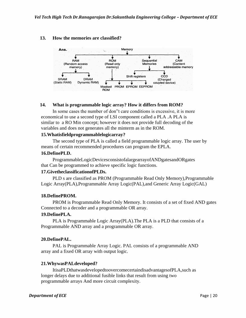
13. How the memories are classified?
14. What is programmable logic array? How it differs from ROM?
In some cases the number of don‟t care conditions is excessive, it is more
economical to use a second type of LSI component called a PLA .A PLA is
similar to a RO Min concept; however it does not provide full decoding of the
variables and does not generates all the minterm as in the ROM.
15.Whatisfieldprogrammablelogicarray?
The second type of PLA is called a field programmable logic array. The user by
means of certain recommended procedures can program the EPLA.
16.DefinePLD.
ProgrammableLogicDevicesconsistofalargearrayofANDgatesandORgates
that Can be programmed to achieve specific logic functions.
17.GivetheclassificationofPLDs.
PLD s are classified as PROM (Programmable Read Only Memory),Programmable
Logic Array(PLA),Programmable Array Logic(PAL),and Generic Array Logic(GAL)
18.DefinePROM.
PROM is Programmable Read Only Memory. It consists of a set of fixed AND gates
Connected to a decoder and a programmable OR array.
19.DefinePLA.
PLA is Programmable Logic Array(PLA).The PLA is a PLD that consists of a
Programmable AND array and a programmable OR array.
20.DefinePAL.
PAL is Programmable Array Logic. PAL consists of a programmable AND
array and a fixed OR array with output logic.
21.WhywasPALdeveloped?
ItisaPLDthatwasdevelopedtoovercomecertaindisadvantagesofPLA,such as
longer delays due to additional fusible links that result from using two
programmable arrays And more circuit complexity.
Vel Tech High Tech Dr.Ranagarajan Dr.Sakunthala Engineering College – Department of ECE
Department of ECE Page | 21
22.Definebit,byteandword.
The smallest unit of binary data is bit. Data are handled in a8bitunitcalled byte. A
complete unit of information is called a word which consists of one or more bytes.
23.What is Read and Write operation?
TheWriteoperationstoresdataintoaspecifiedaddressintothememoryand the Read
Operation takes data out of as specified address in the memory.
24.DefineROM.
ROM is a type of memory in which data a rest or permanently or semi
permanently. Data can be read from a ROM, but there is no write operation.
25.DefineRAM.
RAM is Random Access Memory. It is a random access read/write memory.
The data Can be read or written into from any selected address in any sequence.
26.DefineCachememory.
Itisarelativelysmall,high-speedmemorythatcanstorethemostrecentlyused instructions
or data from larger but slower main memory.
27.Givethefeatureofflashmemory.
Theidealmemoryhashighstoragecapacity,non-volatility;in-systemreadand write
Capability,comparativelyfastoperation.Thetraditionalmemorytechnologies
suchasROM,PROM,EEPROMindividuallyexhibitsoneofthesecharacteristics, but no
single technology has all of them except the flash memory.
28.WhatareFlashmemories?
They are high density read/write memories that are non-volatile, which means
data can be stored indefinitely without power.
29.WhatisaFIFOmemory?
The term FIFO refers to the basic operation of this type of memory in which the
first data bit written in to the memory is to first to be read out.
30.List basic types of programmable logic devices.
1.Readonlymemory
2.ProgrammablelogicArray
3.ProgrammableArrayLogic
31. Define address and word:
In a ROM, each bit combination of the input variable is called on address. Each bit
Combination that comes out of the output lines is called a word.
Vel Tech High Tech Dr.Ranagarajan Dr.Sakunthala Engineering College – Department of ECE
Department of ECE Page | 22
32. What is programmable logic array? How it differs from ROM?
In some cases the number of don‟t care conditions is excessive, it is more
economical to use a second type of LSI component called a PLA. A PLA is similar to a
RO Min concept; however it does not provide full decoding of the variables and does
not generates all the min terms as in the ROM.
UNITV- SYNCHRONOUSAND AYNCHRONOUSSEQUENTIALCIRCUITS
1. What is fundamental mode sequential circuit?
• Input variables changes if the circuit is stable
• Inputs are levels, not pulses
• Only one input can change at a given time
2. What is pulse mode circuit?
• Inputs are pulses
• Width of pulses are long for circuit to respond to the input
• Pulse width must not be so long that it is still present after the new state is
reached
3. What is the significance of state assignment?
• In synchronouscircuits-stateassignmentsaremadewiththeobjectiveofcircuit
• ReductionAsynchronouscircuits-itsobjectiveistoavoidcriticalraces
4. When does race condition occur?
• Two or more binary state variables change their value in response to the
change in i/p Variable
5. What is non critical race?
• Final stable state does not depend on the order in which the state variable
changes
• Race condition is not harmful
6. What is critical race?
• Final stable state depends on the order in which the state variable changes
Race condition is harmful
7. What are the different techniques used in state assignment?
• Shared row state assignment
• One hot state assignment
8. What are the steps for the design of asynchronous sequential circuit?
• Construction of primitive flow table
• Reduction of flow table
Vel Tech High Tech Dr.Ranagarajan Dr.Sakunthala Engineering College – Department of ECE
Department of ECE Page | 23
• State assignment is made
• Realization of primitive flow table
9. What is hazard?
• Unwanted switching transients
10. What is static1hazar?
• Output goes momentarily 0 when It should remain at 1
11. What are static0 hazards?
• Output goes momentarily 1 when it should remain at 0
12. What is dynamic hazard?
• Output changes 3 or more times when it changes from 1 to 0 or 0 to 1
13. What is the cause for essential hazards?
• Unequal delays along 2 or more path from same input
14. What is flow table?
• State table of an synchronous sequential network
15. What is SM chart?
• Describes the behavior of a state machine Used in hardware design of
digital systems
16. What are the advantages of SM chart?
• Easy to understand the operation
• East to convert to several equivalent forms
17. What is combinational circuit?
• Output depends on the given input. It has no storage element.
21.What is state equivalence theorem?
• Two states SA and SB, are equivalent if and only if for every possible
inputX sequence, the outputs are the same and then ext states are
equivalent i.e.,ifSA(t+1)= SB(t+1)and ZA=ZB then SA=SB.
22. What do you mean by distinguishing sequences?
Two states, SA and SB of sequential machine are distinguishable If and only if their
exists at least one finite input sequence.Which,when applied to sequential machine causes
different output sequences depending on whether SA or SB is the initial state.
Vel Tech High Tech Dr.Ranagarajan Dr.Sakunthala Engineering College – Department of ECE
Department of ECE Page | 24
23. Define merger graph.
The merger graph is defined as follows. It contains the same number of vertices as
the state table contains states. Line drawn between the two state vertices indicates each
compatiblestatepair.Ittwostatesareincompatiblenoconnectinglineisdrawn.
24.Defineincompatibility
The states are said to be in compatible if no line is drawn in between them. If
implied states are incompatible, they are crossed & the corresponding line is ignored
25.Explain the procedure for state minimization.
1.Partitionthestatesintosubsetssuchthatallstatesinthesamesubsetsare1 equivalent.
2.Partitionthestatesintosubsetssuchthatallstatesinthesamesubsetsare2 equivalent.
3.Partitionthestatesintosubsetssuchthatallstatesinthesamesubsetsare3 equivalent.
26.Define closed covering.
ASetofcompatiblesissaidtobeclosedif,foreverycompatiblecontainedinthe
set,allitsimpliedcompatiblesarealsocontainedintheset.Aclosedsetof
compatibles,whichcontainsallthestatesofM,iscalledaclosedcovering.
27.Definestatetable.
For the design of sequential counters we have to relate present states and next
states. The table, which represents the relationship between present states and next states,
is called state table.
28.Define total state.
The combination flevelsignalsthatappearattheinputsandtheoutputsofthe delays define
what is called the total state of the circuit.
29.What are the steps for the design of asynchronous sequential circuit?
1.Construction of a primitive flowtable from the problem statement.
2.Primitive flow tableisreducedbyeliminatingredundantstatesusingthestate reduction
3.State assignment is made
4.Theprimitiv eflowtableisrealizedusingappropriatelogicelements.
30. Define primitive flow table:
It is defined as a flow table which has exactly one stable state for each row in the
table. The design process begins with the construction of primitive flow table.
31.What are the types of asynchronous circuits?
1.Fundamentalmodecircuits
Vel Tech High Tech Dr.Ranagarajan Dr.Sakunthala Engineering College – Department of ECE
Department of ECE Page | 25
2.Pulse mode circuits
32. What are races?
When 2 or more binary state variables change their value in response to a change
in an input variable, race condition occurs in an asynchronous sequential circuit. In
case of unequal delays, a race condition may cause the state variables to
change in an unpredictable manner.
33. Define on critical race.
If the final stable state that the circuit reaches does not depend on the order in which
the state variable changes, the race condition are no harmful and it is called an on critical
race.
34. Define critical race?
If the final stable state depends on the order in which the state variable
changes the race condition is harmful and it is called a critical race.
35. What is a cycle?
A cycle occurs when an asynchronous circuit makes a transition through a series of
unstable states. If a cycle does not contain a stable state, theci rcuitwillgo from one
unstable to stable to another, until the inputs are changed.
36.List the different techniques used for state assignment.
1.Shared row state assignment state assignment
37.Write a short note on fundamental mode asynchronous circuit.
Fundamental mode circuit assumes that. The input variables change only when
the circuit is stable. Only one input variable can change at a given time and inputs are
levels and not pulses.
38. Write a short note on pulse mode circuit.
Pulse mode circuit assumes that the input variables are pulses instead of level.
Thewidthofthepulsesislongenoughforthecircuittorespondtotheinputand the pulse width
must not be so long that it is still present after the new state is reached.
39.Define secondary variables.
Thedelayelementsprovideashorttermmemoryforthesequentialcircuit.The
presentstateandnextstatevariablesinasynchronoussequentialcircuitsare called
secondary variables.
40.Defineflowtableinasynchronoussequentialcircuit.
Inasynchronoussequentialcircuitstatetableisknownasflowtablebecauseof
thebehaviouroftheasynchronoussequentialcircuit.Thestagechangesoccurin independent
of a clock ,based on the logic propagation delay, and cause the states to flow from one
to another.
Vel Tech High Tech Dr.Ranagarajan Dr.Sakunthala Engineering College – Department of ECE
Department of ECE Page | 26
41. Whatis pulse mode asynchronous machine?
A pulse mode asynchronous machine has two inputs. If produces an output
whenevertwo consecutive pulses occur on one input line only. The output remains
at 1untilapulsehasoccurredontheotherinputline.Writedownthestatetablefor the
machine.
42.Whatisfundamentalmode?
Atransitionfromonestablestatetoanotheroccursonlyinresponsetoachange in the input
state.After a change in one input has occurred, no other change in any in put occurs until
the circuit enters a stable state.Such a mode of operation is referred to as fundamental
mode.
43. Write short note on one hot state assignment.
The one hot state assignment is another method for finding a race free state
assignment.In this method, only one variable
is active or hot for e a chrow I nthe originalflowtable, ie, it requires one
state variable for each row of the flow table. Additional row are introduced to provide
single variablechangesbetween internal state transitions.
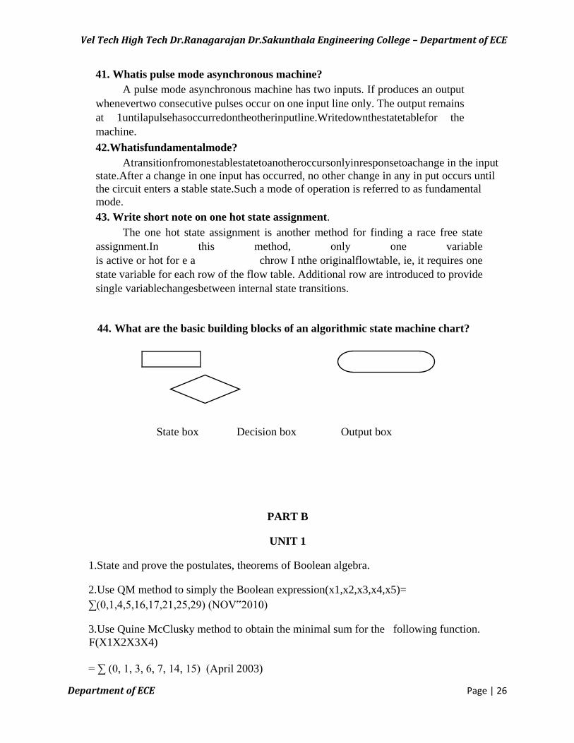
44. What are the basic building blocks of an algorithmic state machine chart?
State box Decision box Output box
PART B
UNIT 1
1.State and prove the postulates, theorems of Boolean algebra.
2.Use QM method to simply the Boolean expression(x1,x2,x3,x4,x5)=
∑(0,1,4,5,16,17,21,25,29) (NOV‟2010)
3.Use Quine McClusky method to obtain the minimal sum for the following function.
F(X1X2X3X4)
= ∑ (0, 1, 3, 6, 7, 14, 15) (April 2003)
Vel Tech High Tech Dr.Ranagarajan Dr.Sakunthala Engineering College – Department of ECE
Department of ECE Page | 27
4.Simplify the function using Karnaugh map.
(i) F (ABCD) = ∑ (0, 1, 2, 4, 5, 7, 11, 15) (8mark)
(ii) F (WXYZ) = ∑ (2, 3, 10, 11, 12, 13, 14, 15) (8mark) (April 2003)
4. (i) State and prove demorgan‟s theorem and expand the
function F = ( (( A
(ii) Simplify the following switching function using karnaugh map,
F(A,B,C,D) = ∑ (0,5,7,8,9,10,11,14,15) + Φ (1,4,13) (10 mark)
5..i) Simplify the following Boolean function using 4 variable map F(w,x,y,z)=
(2,3,10,11,12,13,14,15)
ii)Draw a NAND logic diagram that implements the complement of the following function
F(A,B,C,D)= ∑(0,1,2,3,4,8,9,12) (8mark)
6.Simplify the Boolean function using K-map and tabular methods. Compare the methods. F
(A, B, C, D) =∑m(4,5,6,7,8) d (A, B, C, D) = ∑m(11,12,13,14,15).
7.Implement using only NAND gates
(i) Express the function f(x, y, z) =
(ii) Express the following function as the minimal sum of products,
using a K-map F (a,b,c,d) =∑m(0,2,4,5,6,8,10,15) + ∑Φ(7,13,14)
(12 marks)
8.Implement the following with either NAND gate or NOR gate gates. Use only 4 gates.
Only the normal inputs are available.
(i) d = WYZ (8mark)
(ii)
Vel Tech High Tech Dr.Ranagarajan Dr.Sakunthala Engineering College – Department of ECE
Department of ECE Page | 28
UNIT 2
1. Designa BCD to Graycode converter. Usedon‟t cares
2. Design a halfadder and full adder circuits .
3. Design a half subractor and design a subractor
4. Designa4-bitbinaryto BCD code converter.
5. Construct a 4-bitbinarytograycodeconvertercircuitand discuss its operation.
6. Design a combinational circuit to convert Excess-3 code to BCD code.
7. i) Design an 8X1 MUX usingonly2X1 MUX (8)
ii) Design a circuit to carryout both addition and subtraction (8)
8. Design a BCD adder to add two BCD digits
9. Design a combinational circuit that accepts 3 bit binary number and converts it to
excess 3
code.
10. Design a circuit to compare two four bit numbers
11. Design a Gray to BCD code converter
12. Design a combinational circuit to convert BCD code to Excess-3 code
13. Design a combinational logic circuit to compare two 2-bit binary numbers A and B
and to generate the outputs A<B,A=B and A>B
14.(i)Realize F(w,x,y,z)=S(1,4,6,7,8,9,10,15)using4 to 1 Mux (8mark)
(ii) Design a binary multiplier circuit
15. (i)Design an 8x1 MUXusingonly2x1 MUX
(ii) Design a circuit to carryout both addition and subtraction
16. Design and implement the conversion circuit for BCD to Excess 3 code (16)
17. (i).Design a combinational circuit that generates the 9‟s complement of a BCD digit
(8) (ii) Explain the operation of carry look ahead adder with neat diagram.
18. (i) Define fan-in, fan–out and Noise margin (6) NOV‟2010
Vel Tech High Tech Dr.Ranagarajan Dr.Sakunthala Engineering College – Department of ECE
Department of ECE Page | 29
(ii) Design combinational system that produces the product of 2 binary
number A=(A1,A0) X B=(B2,B1,B0) (10)
UNIT 3
1. i) Provide the characteristic table, characteristic equation and excitation table of
D flip flop and JK flip flop (6)
ii) Explain the operation universal shift register with neat block diagram (8)
Nov‟2010
3. With a neat state diagram and logic diagram , design and explain the sequence of states
of BCD counter ( 16)
3. Draw the circuit and explain the working operation of JK Master Slave flip-flop
4. Explain the various steps in the analysis of synchronous sequential circuits with
suitable example.
5. Using D flip-flops, design a synchronous counter which counts in thesequence000,
001,
010,011, 100, 101, 110, 111, 000
6. Using JK flip-flops, design asynchronous counter which counts in thesequence000,
111,
101,110, 001, 010, 000……
7. Design a binary counter using T flip-flops to count pulses in the following sequence
(i)000, 001, 010, 011, 100, 101, 110, 111, 000
(ii) 000, 100, 111, 010, 011, 000 (8)
8. Explain the functional operation of a 4 bit binary ripple counter with its logical
diagram
9. Explain the working of Master-slave flip-flop.
10. i) Drawa4 bit serial in serial out shift register and draw its waveforms. (8) ii). Draw
a4 bit serial in parallel out(SIPO) and explain its operation. (8)
11. Explain the operation of BCD counter.
12. Design an Asynchronous BCD down counter usingJ-K flip=flop and verify its
operation.
13. Design asynchronous mod-8 down counter and implement it.
Vel Tech High Tech Dr.Ranagarajan Dr.Sakunthala Engineering College – Department of ECE
Department of ECE Page | 30
14. Design and explain the working of a up-down ripple counter
15. (i)Explain the operation of D type edge triggered flip flop. (ii) How can a D flip flop
converted into aT flip flop.
16. Using JK flip-flops, design asynchronous counter which counts in
thesequence2,6,1,7,5,4and repeat.
17. Design a Mod 5 Asynchronous counter draws the waveforms. (8marks)
18. Using RSflip-flops, design a Parallel counter which counts in thesequence000, 111,
101,
110,001, 010, 000……
19. .i) Draw the logic diagram for a master–slave JK flip flop and explain. (8) ii) Draw
the four bit Johnson counter and explain the operation
20. Draw and explain the logic diagram of up/down counter
UNIT 4
1. Explain the basic structure of 256x4 static RAM with neat sketch (8)
2. Write a note on (i) MOSFET RAM cell (8) (ii) Dynamic RAM cell (8)
3. i) Explain read and write operation of memory with timing wave forms. (8) ii)
Write a note on RAM.
4. i) Draw a PLA circuit to implement the functions F1=A‟B+AC‟+A‟BC ;
F2=(AC+AB+BC)‟
ii) Write a note on FPGA. (8) (Nov 2010)
5. A combinational circuit is defined by the
functions F1= ∑m(3,5,7)
F2=∑m(4,5,7)
Implement the circuit with a PLA having3 inputs, 3 product terms and two outputs.
6.Implement binary to excess 3 code converter using ROM. (16)
7.Tabulatethe PAL programming table for the four Boolean functions listed below.
A(x,y, z) =∑(1,
2, 4, 6), B(x,y,
z) =∑(0, 1,6, 7)
C(x,y, z) =∑(2, 6), D(x,y, z) =∑(1, 2,3, 5, 7) (16)
8. A combinational circuit is defined by the functions (8)
F2(A,B,C)=Σ(0,2,4,7)implement the circuit with a PLA.
Vel Tech High Tech Dr.Ranagarajan Dr.Sakunthala Engineering College – Department of ECE
Department of ECE Page | 31
9. A combinational circuit is described by the functions
F1=∑m(3,4,5,7,10,14,15),F2=∑m(1,5,7,11,15)Implement the circuit with a
PLAhaving4inputs,6 product terms and two outputs
10.Acombinational circuit is defined by the
functions F1= ∑m(3,5,7) F2= ∑m(4,5,7)
Implement the circuit with a PLA having3 inputs, 3 product terms and two outputs.
11.Acombinational circuit is defined by the
functions F1= ∑m(1,3,5) F2= ∑m(5,6,7)
Implement the circuit with a PLA having 3 inputs, 3 product terms and two outputs.
UNIT 5
1. i)Give examples for critical race and cycle and
explain ii) Describe the hazards with neat circuit
diagram.
4. 7, 8, 10, 12)
3. Design an asynchronous sequential circuit that has two inputs X2 and X1 and
one output z. When x1 = 0, the output Z is 0. The first change in X2 that occurs while
X1 is 1 will cause output Z to be 1.
The output
Z will remain 1 until X1 returns to zero. (16)
4. An asynchronous sequential circuit has two internal states and one output. The
excitation and output function describing the circuit are as follows.
5. i)Give hazard-free realization for the following Boolean function
F(A,B,C,D)=Σm(1,3,6,7,13,15) ii) Summarize the design procedure for asynchronous
sequential circuit.
6.An asynchronous sequential circuit is described by the following excitation and output
function.
Y=X1X2+(X1+X2)Y
i) Draw the logic diagram ii) Derive the transition table and output map iii) Describe the
behavior of the circuit. 7. An asynchronous network has two inputs and one output. The
input sequence X1X2 =00, 01,11causes the output to become 1.The next input
change then causes the output to return to 0. No other
input sequence will produce a 1 output. Construct the state diagram using primitive flow
table (16)
8.a)Design a circuit with inputs A and B to give an output Z equal to 1 when AB=11 but
only if A becomes 1 before B, by drawing total state Diagram, primitive flow table and
output map in which transient state is Included.
Vel Tech High Tech Dr.Ranagarajan Dr.Sakunthala Engineering College – Department of ECE
Department of ECE Page | 32
b) Design a circuit with primary inputs A and B to give an output Z equal to 1
When A becomes 1 if B is already 1.Once Z=1 it will remain so until A goes to
c)
Draw waveform diagram, total state diagram, primitive flow table for designing the
circuit
9. An asynchronous circuit described by the following excitation and output function
Y=X1.X2+(X1+X2).Y Z=Y
Draw the logic diagram of the circuit. Derive the transition table and output map.
Describe the behavior of the circuit
10. Design a asynchronous sequential circuit with 2 inputs X and Y and with one
output Z whenever Y is 1, input X is transferred to Z.When Y is 0,the output does not
change for any change in X. use SR latch for implementation of the circuit
11. What is a merger graph .How it is used to reduce states in the incompletely
specified table 12. What are the problems in asynchronous circuits and what are
essential hazards and static hazards how it can be eliminated
13. Design T flip flop from logic gates.
14..Give the hazard free realization for the following functions.
(i) NAND
gates (ii)
NOR gates
16. Design a sequence Detector circuit with a single input line and a single output line.
Whenever the input consists of the sequence 101 , the output should be 1. For
example, if the input is 00110101…,then the output is 00000101… in other
words,over lapping sequences are allowed. Use any type of flip flop. (16)
16.(i) .Give the hazard free realization for the following functions.
(ii) Summarize the design procedure for asynchronous sequential circuit. (8marks)
17. An asynchronous circuit described by the following excitation and output function
X=(Y1.Z1‟W2) X + ( Y1‟Z1W2‟) S=X‟
Draw the logic diagram of the circuit. Derive the transition table and output map.
Describe the behavior of the circuit
18. Explain essential, static and dynamic Hazards in Digital circuit. Give the hazard free
realization for thefollowing functions.
19. Design an asynchronous circuit using JK FF that will O/P only the first pulse received
and will ignore any other pulses (16)
20. i) Differentiate critical races from non-critical races. (6) NOV‟2010 ii) Explain the
steps involved in the reduction of state table. (10)
Vel Tech High Tech Dr.Ranagarajan Dr.Sakunthala Engineering College – Department of ECE
Department of ECE Page | 33
Vel Tech High Tech Dr.Ranagarajan Dr.Sakunthala Engineering College – Department of ECE
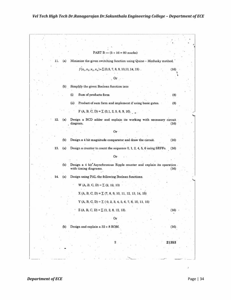
Department of ECE Page | 34
Vel Tech High Tech Dr.Ranagarajan Dr.Sakunthala Engineering College – Department of ECE
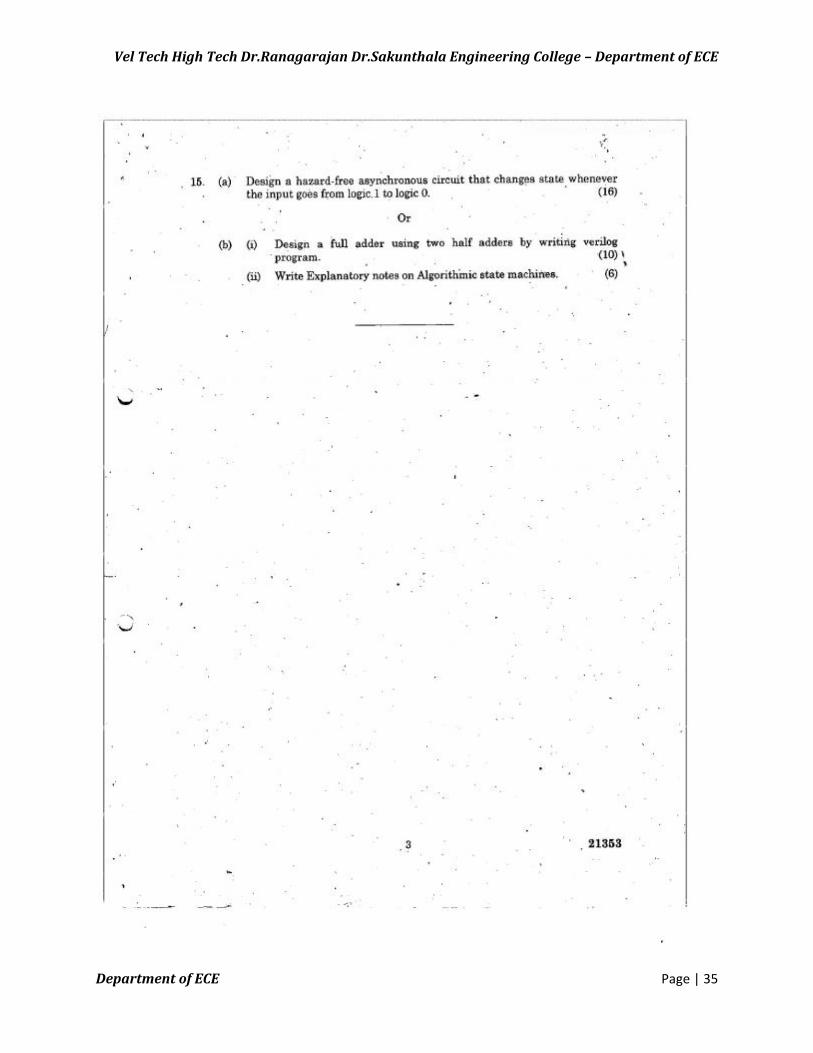
Department of ECE Page | 35
Vel Tech High Tech Dr.Ranagarajan Dr.Sakunthala Engineering College – Department of ECE
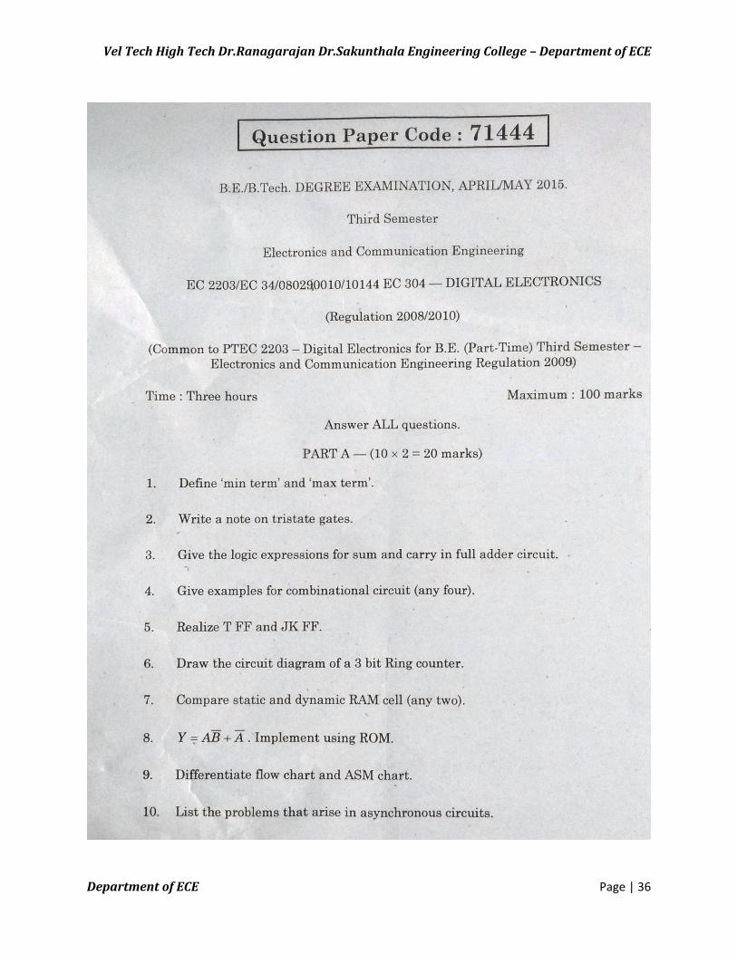
Department of ECE Page | 36
Vel Tech High Tech Dr.Ranagarajan Dr.Sakunthala Engineering College – Department of ECE
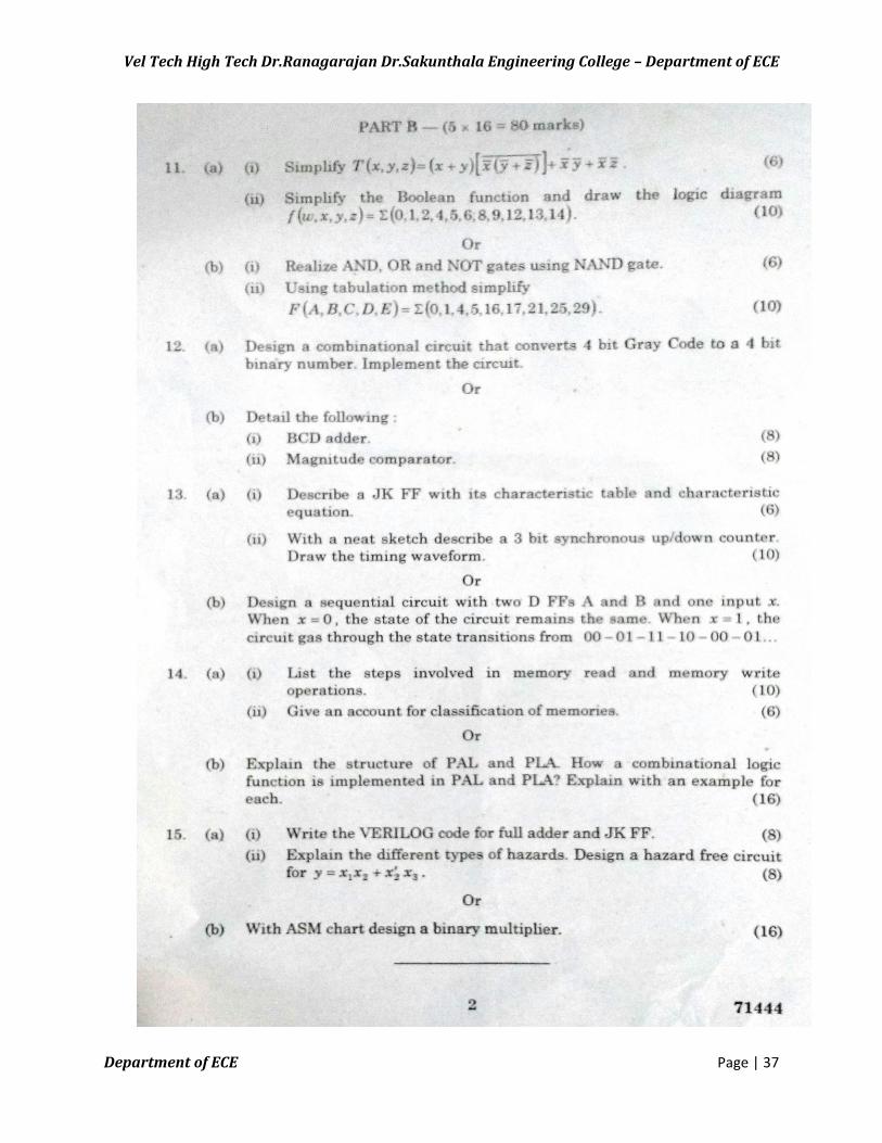
Department of ECE Page | 37
Vel Tech High Tech Dr.Ranagarajan Dr.Sakunthala Engineering College – Department of ECE
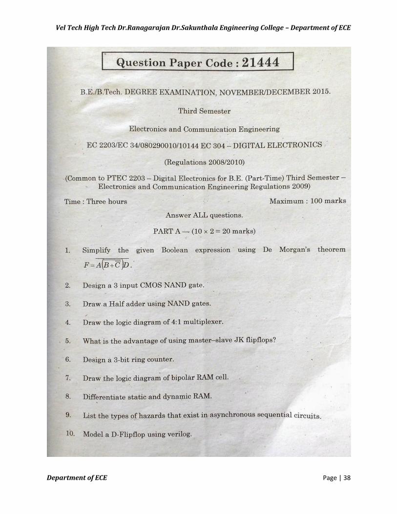
Department of ECE Page | 38
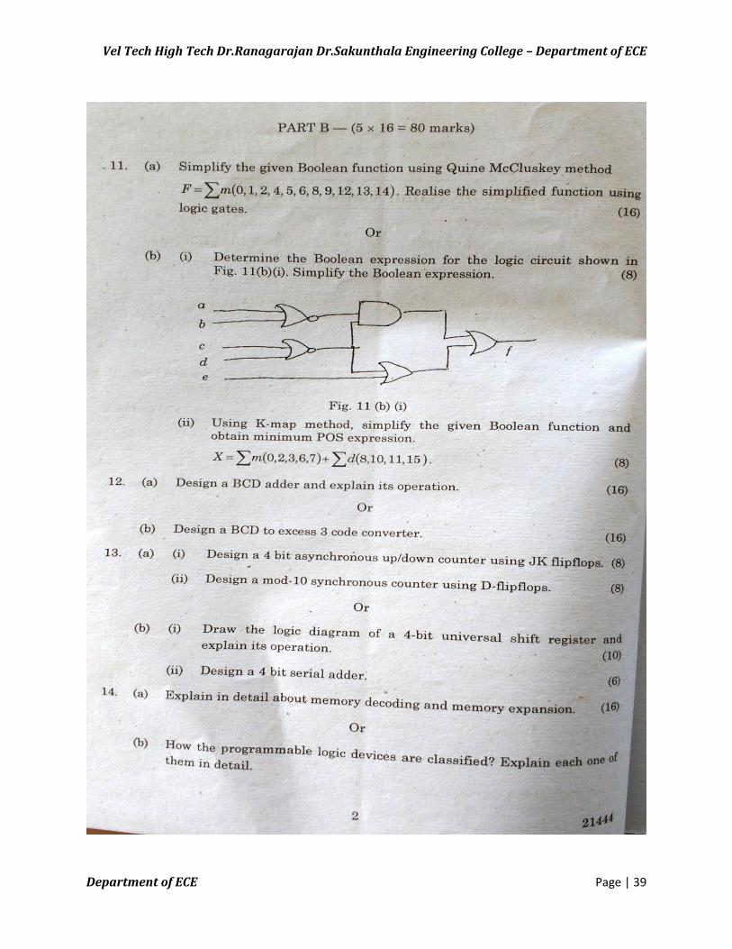
Vel Tech High Tech Dr.Ranagarajan Dr.Sakunthala Engineering College – Department of ECE
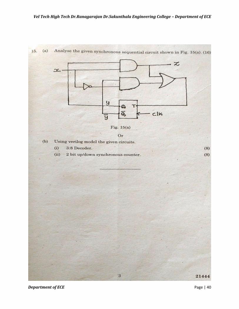
Department of ECE Page | 39
Vel Tech High Tech Dr.Ranagarajan Dr.Sakunthala Engineering College – Department of ECE
Department of ECE Page | 40

Vel Tech High Tech Dr.Ranagarajan Dr.Sakunthala Engineering College – Department of ECE
Department of ECE Page | 41
Vel Tech High Tech Dr.Ranagarajan Dr.Sakunthala Engineering College – Department of ECE
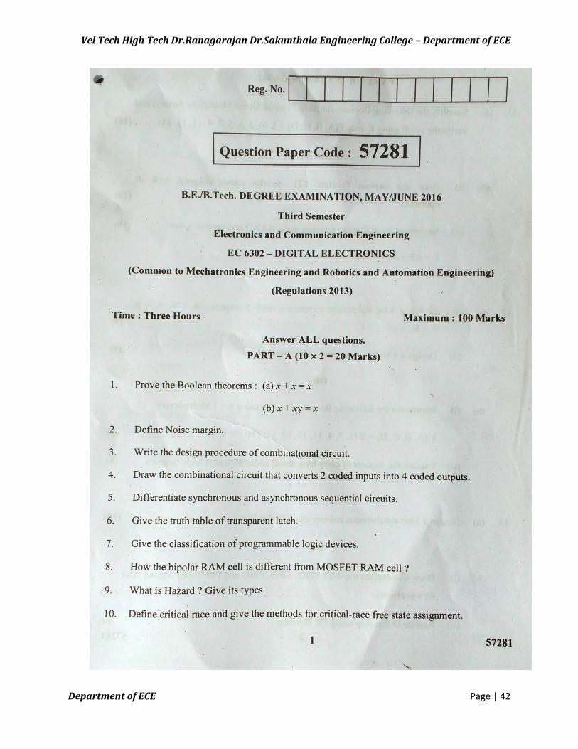
Department of ECE Page | 42
Vel Tech High Tech Dr.Ranagarajan Dr.Sakunthala Engineering College – Department of ECE
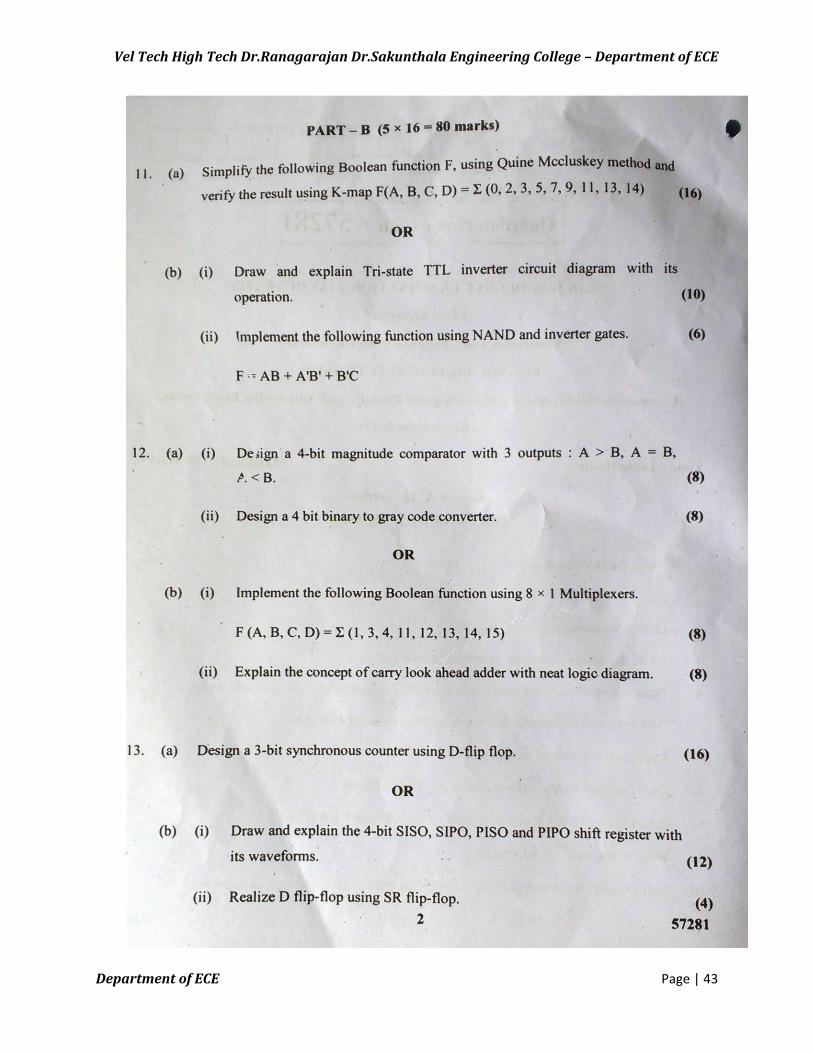
Department of ECE Page | 43
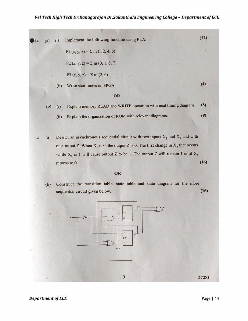
Vel Tech High Tech Dr.Ranagarajan Dr.Sakunthala Engineering College – Department of ECE
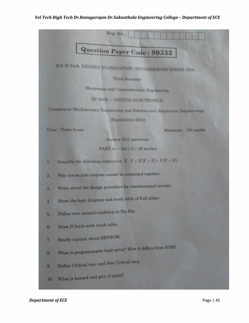
Department of ECE Page | 44
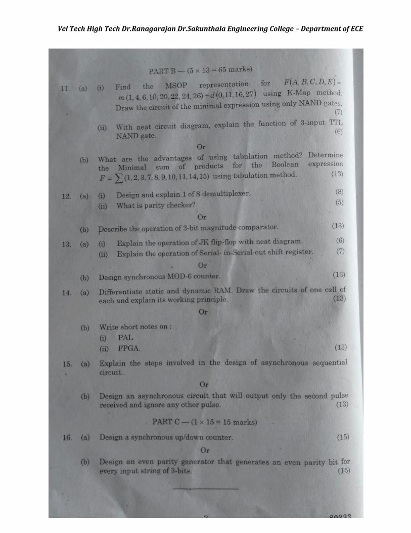
Vel Tech High Tech Dr.Ranagarajan Dr.Sakunthala Engineering College – Department of ECE
Department of ECE Page | 45
Vel Tech High Tech Dr.Ranagarajan Dr.Sakunthala Engineering College – Department of ECE
Department of ECE Page | 46