verilog hdl:digital design and modeling chapter 11 ... ch 11.pdf · chapter 11 additional design...
TRANSCRIPT

Chapter 11 Additional Design Examples 1
Verilog HDL:Digital Design and Modeling
Chapter 11
Additional Design Examples
Chapter 11 Additional Design Examples 2
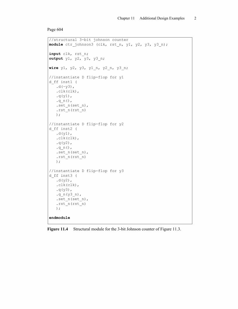
Page 604
//structural 3-bit johnson countermodule ctr_johnson3 (clk, rst_n, y1, y2, y3, y3_n);
input clk, rst_n;output y1, y2, y3, y3_n;
wire y1, y2, y3, y1_n, y2_n, y3_n;
//instantiate D flip-flop for y1d_ff inst1 (
.d(~y3),
.clk(clk),
.q(y1),
.q_n(),
.set_n(set_n),
.rst_n(rst_n));
//instantiate D flip-flop for y2d_ff inst2 (
.d(y1),
.clk(clk),
.q(y2),
.q_n(),
.set_n(set_n),
.rst_n(rst_n));
//instantiate D flip-flop for y3d_ff inst3 (
.d(y2),
.clk(clk),
.q(y3),
.q_n(y3_n),
.set_n(set_n),
.rst_n(rst_n));
endmodule
Figure 11.4 Structural module for the 3-bit Johnson counter of Figure 11.3.

Chapter 11 Additional Design Examples 3
Page 605//3-bit Johnson counter test benchmodule ctr_johnson3_tb;
reg clk, rst_n;wire y1, y2, y3, y3_n;
//display outputs at simulation timeinitial$monitor ($time, "Count = %b", {y1, y2, y3});
//define resetinitialbegin
#0 rst_n = 1'b0;#5 rst_n = 1'b1;
end
//define clkinitialbegin
clk = 1'b0;forever
#10 clk = ~clk;end
//finish simulation at time 200initialbegin
#200 $finish;end
//instantiate the module into the test benchctr_johnson3 inst1 (
.clk(clk),
.rst_n(rst_n),
.y1(y1),
.y2(y2),
.y3(y3),
.y3_n(y3_n));
endmodule
Figure 11.5 Test bench for the 3-bit Johnson counter of Figure 11.4.

Chapter 11 Additional Design Examples 4
Page 606
0 Count = 00010 Count = 10030 Count = 11050 Count = 11170 Count = 01190 Count = 001110 Count = 000130 Count = 100150 Count = 110170 Count = 111190 Count = 011
Figure 11.6 Outputs for the 3-bit Johnson counter of Figure 11.4.
Figure 11.7 Waveforms for the 3-bit Johnson counter of Figure 11.4.

Chapter 11 Additional Design Examples 5
Page 607
//behavioral 3-bit binary countermodule ctr_bin3 (clk, rst_n, ctr);
input clk, rst_n;output [2:0] ctr;
wire clk, rst_n; //inputs are wirereg [2:0] ctr, next_cnt; //outputs are reg
//latch next countalways @ (posedge clk or negedge rst_n)begin
if (rst_n == 0)ctr <= 3'b000;
elsectr <= ctr + 1;
endendmodule
Figure 11.9 Module for a 3-bit binary counter.
Page 608
//behavioral 3-bit shiftermodule shftr3 (clk, rst_n, serial_in, shftr);
input clk, rst_n, serial_in;output [2:0] shftr;
wire clk, rst_n, serial_in;reg [2:0] shftr;
//establish reset and shift operationalways @ (posedge clk or rst_n)begin
if (rst_n == 0)shftr <= 3'b000;
elseshftr <= {serial_in, shftr [2:1]};
endendmodule
Figure 11.10 Module for a 3-bit shift register.

Chapter 11 Additional Design Examples 6
Page 608
//structural counter shiftermodule ctr_shftr_struct (clk, rst_n, sngl_1, dbl_1,
ctr, shftr);
input clk, rst_n, sngl_1, dbl_1;output [2:0] ctr, shftr;
//The following statements are not necessary because //signals are wire by default. They have been added //as a reminder that input/output signals are wires in//structural modeling.wire clk, rst_n, sngl_1, dbl_1;wire [2:0] ctr, shftr;
//instantiate the counterctr_bin3 inst1 (
.clk(clk),
.rst_n(rst_n),
.ctr(ctr));
//continued on next page
Figure 11.11 Structural module for the counter-shifter of Section 11.2.

Chapter 11 Additional Design Examples 7
//instantiate the shifter clk logicand4_df inst2 (
.x1(ctr[0]),
.x2(ctr[1]),
.x3(ctr[2]),
.x4(~clk),
.z1(shftr_clk));
//instantiate the pattern select logicand4_df inst4 (
.x1(sngl_1),
.x2(~shftr[0]),
.x3(~shftr[1]),
.x4(~shftr[2]),
.z1(net1));
and3_df inst5 (.x1(~shftr[0]),.x2(~shftr[1]),.x3(dbl_1),.z1(net2));
or2_df inst6 (.x1(net1),.x2(net2),.z1(serial_in));
//instantiate the shiftershftr3 inst3 (
.clk(shftr_clk),
.rst_n(rst_n),
.serial_in(serial_in),
.shftr(shftr));
endmodule
Figure 11.11 (Continued)

Chapter 11 Additional Design Examples 8
Page 610//test bench for the counter shiftermodule ctr_shftr_struct_tb;
reg clk, rst_n, sngl_1, dbl_1, shftr_clk;wire [2:0] ctr, shftr;
initial$monitor ("ctr=%b, sngl_1=%b, dbl_1=%b, shftr=%b",
ctr, sngl_1, dbl_1, shftr);
//define clkinitialbegin
clk = 1'b0;forever
#10 clk = ~clk;end
//define reset and patterninitialbegin
#0 rst_n = 1'b0;sngl_1 = 1'b1;dbl_1 = 1'b0;
#5 rst_n = 1'b1;
#640 sngl_1 = 1'b0;dbl_1 = 1'b1;
#900 $stop;end
//instantiate the module into the test benchctr_shftr_struct inst1 (
.clk(clk),
.rst_n(rst_n),
.ctr(ctr),
.sngl_1(sngl_1),
.dbl_1(dbl_1),
.shftr(shftr));
endmodule
Figure 11.12 Test bench for the structural module of Figure 11.11.

Chapter 11 Additional Design Examples 9
Page 611
SINGLE 1
ctr=000, sngl_1=1, dbl_1=0, shftr=000ctr=001, sngl_1=1, dbl_1=0, shftr=000ctr=010, sngl_1=1, dbl_1=0, shftr=000ctr=011, sngl_1=1, dbl_1=0, shftr=000ctr=100, sngl_1=1, dbl_1=0, shftr=000ctr=101, sngl_1=1, dbl_1=0, shftr=000ctr=110, sngl_1=1, dbl_1=0, shftr=000ctr=111, sngl_1=1, dbl_1=0, shftr=100--------------------------------------ctr=000, sngl_1=1, dbl_1=0, shftr=100. . .ctr=111, sngl_1=1, dbl_1=0, shftr=010--------------------------------------ctr=000, sngl_1=1, dbl_1=0, shftr=010. . .ctr=111, sngl_1=1, dbl_1=0, shftr=001--------------------------------------ctr=000, sngl_1=1, dbl_1=0, shftr=001. . .ctr=111, sngl_1=1, dbl_1=0, shftr=000--------------------------------------
DOUBLE 1
ctr=000, sngl_1=0, dbl_1=1, shftr=000. . .ctr=111, sngl_1=0, dbl_1=1, shftr=100-------------------------------------ctr=000, sngl_1=0, dbl_1=1, shftr=100. . .ctr=111, sngl_1=0, dbl_1=1, shftr=110-------------------------------------ctr=000, sngl_1=0, dbl_1=1, shftr=110. . .ctr=111, sngl_1=0, dbl_1=1, shftr=011-------------------------------------ctr=000, sngl_1=0, dbl_1=1, shftr=011. . .ctr=111, sngl_1=0, dbl_1=1, shftr=001-------------------------------------ctr=000, sngl_1=0, dbl_1=1, shftr=001. . .ctr=111, sngl_1=0, dbl_1=1, shftr=000--------------------------------------
Figure 11.13 Outputs for the counter-shifter module of Figure 11.11.

Chapter 11 Additional Design Examples 10
Page 612
//mixed-design universal shift registermodule shift_reg1 (clk, rst_n, data_in, fctn, shift_amt, q);
input clk, rst_n;input [7:0] data_in;input [1:0] fctn, shift_amt;
output [7:0] q;
reg [7:0] q;wire [7:0] shift_l_data, shift_r_data;reg [7:0] d;
parameter nop = 2'b00;parameter shr = 2'b01;parameter shl = 2'b10;parameter ld = 2'b11;
assign shift_l_data = q << shift_amt;assign shift_r_data = q >> shift_amt;
always @ (shift_l_data or shift_r_data or fctn or data_in or q)begin
case (fctn)nop: d = q;shr: d = shift_r_data;shl: d = shift_l_data;ld : d = data_in;default: d = 8'h00;
endcaseend
always @ (posedge clk or negedge rst_n)begin
if (~rst_n)q <= 8'h00;
elseq <= d;
end
endmodule
Figure 11.15 Mixed-design module for the universal shift register of Figure 11.14.

Chapter 11 Additional Design Examples 11
Page 613
//test bench for the universal shift registermodule shift_reg1_tb;
reg clk, rst_n;reg [7:0] data_in;reg [1:0] fctn, shift_amt;
wire [7:0] q;
//display variablesinitial$monitor ("data_in=%b, fctn=%b, shift_amt=%b, q=%b",
data_in, fctn, shift_amt, q);
//define clockinitialbegin
clk = 1'b0;forever
#10 clk = ~clk;end
//continued on next page
Figure 11.16 Test bench for the universal shift register of Figure 11.15.

Chapter 11 Additional Design Examples 12
Figure 11.1initial //define operand, fctn, and shift amountbegin
#0 rst_n = 1'b0;data_in = 8'b0000_0000;fctn = 2'b00;shift_amt = 2'b00;
#10 rst_n = 1'b1;//shift right 0, 1, 2, and 3********************************
data_in = 8'b1111_0000;fctn = 2'b11;@ (posedge clk) //load q
fctn = 2'b01;shift_amt = 2'b00;@ (posedge clk) //shift right 0
//----------------------------------------------------------data_in = 8'b1111_0000;fctn = 2'b11;@ (posedge clk) //load q
fctn = 2'b01;shift_amt = 2'b01;@ (posedge clk) //shift right 1
//----------------------------------------------------------data_in = 8'b1111_0000;fctn = 2'b11;@ (posedge clk) //load q
fctn = 2'b01;shift_amt = 2'b10;@ (posedge clk) //shift right 2
//----------------------------------------------------------data_in = 8'b1111_0000;fctn = 2'b11;@ (posedge clk) //load q
fctn = 2'b01;shift_amt = 2'b11;@ (posedge clk) //shift right 3
//----------------------------------------------------------data_in = 8'b1111_1111;fctn = 2'b11;@ (posedge clk) //load q
fctn = 2'b01;shift_amt = 2'b01;@ (posedge clk) //shift right 1 (0111_1111), next pg
Figure 11.16 (Continued)
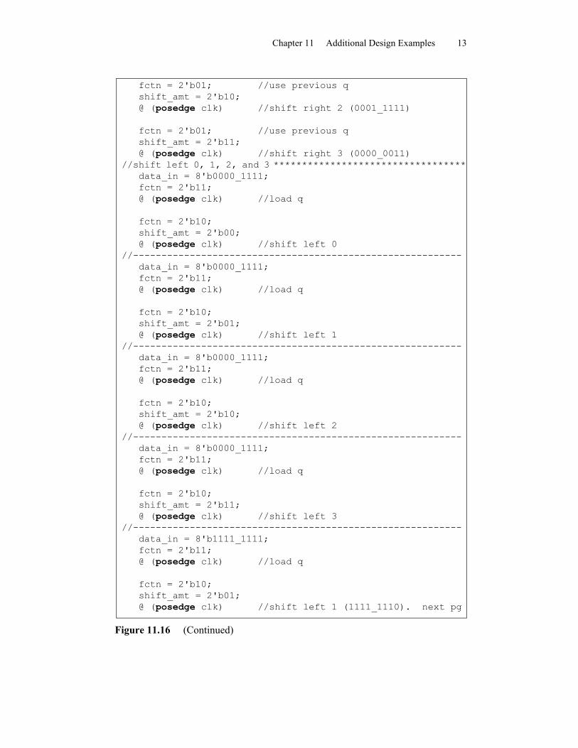
Chapter 11 Additional Design Examples 13
fctn = 2'b01; //use previous qshift_amt = 2'b10;@ (posedge clk) //shift right 2 (0001_1111)
fctn = 2'b01; //use previous qshift_amt = 2'b11;@ (posedge clk) //shift right 3 (0000_0011)
//shift left 0, 1, 2, and 3 **********************************data_in = 8'b0000_1111;fctn = 2'b11;@ (posedge clk) //load q
fctn = 2'b10;shift_amt = 2'b00;@ (posedge clk) //shift left 0
//----------------------------------------------------------data_in = 8'b0000_1111;fctn = 2'b11;@ (posedge clk) //load q
fctn = 2'b10;shift_amt = 2'b01;@ (posedge clk) //shift left 1
//----------------------------------------------------------data_in = 8'b0000_1111;fctn = 2'b11;@ (posedge clk) //load q
fctn = 2'b10;shift_amt = 2'b10;@ (posedge clk) //shift left 2
//----------------------------------------------------------data_in = 8'b0000_1111;fctn = 2'b11;@ (posedge clk) //load q
fctn = 2'b10;shift_amt = 2'b11;@ (posedge clk) //shift left 3
//----------------------------------------------------------data_in = 8'b1111_1111;fctn = 2'b11;@ (posedge clk) //load q
fctn = 2'b10;shift_amt = 2'b01;@ (posedge clk) //shift left 1 (1111_1110). next pg
Figure 11.16 (Continued)

Chapter 11 Additional Design Examples 14
fctn = 2'b10;shift_amt = 2'b10; //use previous q@ (posedge clk) //shift left 2 (1111_1000)
fctn = 2'b10;shift_amt = 2'b11; //use previous q@ (posedge clk) //shift left 3 (1100_0000)
#40 $stop;
end
////instantiate the module into the test benchshift_reg1 inst1 (
.clk(clk),
.rst_n(rst_n),
.data_in(data_in),
.q(q),
.fctn(fctn),
.shift_amt(shift_amt));
endmodule
Figure 11.16 (Continued)
Page 616
Figure 11.17 Waveforms for the universal shift register of Figure 11.15.

Chapter 11 Additional Design Examples 15
Page 626
//dataflow module for Hamming code to encode an 8-bit messagemodule hamming_code (m3, m5, m6, m7, m9, m10, m11, m12,
p1, p2, p4,p8,mv3, mv5, mv6, mv7, mv9, mv10, mv11, mv12,e1_err, e2_err, e4_err, e8_err);
input m3, m5, m6, m7, m9, m10, m11, m12;input p1, p2, p4, p8;
output mv3, mv5, mv6, mv7, mv9, mv10, mv11, mv12;output e1_err, e2_err, e4_err, e8_err;
wire mr3_err, mr5_err, mr6_err, mr7_err;wire mr9_err, mr10_err, mr11_err, mr12_err;
//define the error bitsassign e1_err = ~(p1 ^ m3 ^ m5 ^ m7 ^ m9 ^ m11),
e2_err = ~(p2 ^ m3 ^ m6 ^ m7 ^ m10 ^ m11),e4_err = ~(p4 ^ m5 ^ m6 ^ m7 ^ m12),e8_err = ~(p8 ^ m9 ^ m10 ^ m11 ^ m12);
//design the decoderassign mr3_err= (~e8_err) & (~e4_err) & (e2_err) & (e1_err),
mr5_err= (~e8_err) & (e4_err) & (~e2_err) & (e1_err),mr6_err= (~e8_err) & (e4_err) & (e2_err) & (~e1_err),mr7_err= (~e8_err) & (e4_err) & (e2_err) & (e1_err),mr9_err= (e8_err) & (~e4_err) & (~e2_err) & (e1_err),mr10_err = (e8_err) & (~e4_err) & (e2_err) & (~e1_err),mr11_err = (e8_err) & (~e4_err) & (e2_err) & (e1_err),mr12_err = (e8_err) & (e4_err) & (~e2_err) & (~e1_err);
//design the correction logicassign mv3 = (mr3_err) ^ (m3),
mv5 = (mr5_err) ^ (m5),mv6 = (mr6_err) ^ (m6),mv7 = (mr7_err) ^ (m7),mv9 = (mr9_err) ^ (m9),mv10= (mr10_err) ^ (m10),mv11= (mr11_err) ^ (m11),mv12= (mr12_err) ^ (m12);
endmodule
Figure 11.22 Dataflow module to illustrate Hamming code error detection and cor-rection.

Chapter 11 Additional Design Examples 16
Page 627
//test bench for the Hamming code modulemodule hamming_code_tb;
reg m3, m5, m6, m7, m9, m10, m11, m12;reg ms3, ms5, ms6, ms7, ms9, ms10, ms11, ms12;reg mr3, mr5, mr6, mr7, mr9, mr10, mr11, mr12;wire mv3, mv5, mv6, mv7, mv9, mv10, mv11, mv12;wire e1_err, e2_err, e4_err, e8_err;reg p1, p2, p4, p8;
initial$display ("bit_order = m3, m5, m6, m7, m9, m10, m11, m12");
initial$monitor ("sent=%b, rcvd=%b, error=%b, valid=%b",
{ms3, ms5, ms6, ms7, ms9, ms10, ms11, ms12},{mr3, mr5, mr6, mr7, mr9, mr10, mr11, mr12},{e8_err, e4_err, e2_err, e1_err},{mv3, mv5, mv6, mv7, mv9, mv10, mv11, mv12});
initialbegin//---------------------------------------------------------
#0 {ms3,ms5,ms6,ms7,ms9,ms10,ms11,ms12}=8'b1010_1010;{m3,m5,m6,m7,m9,m10,m11,m12} = {ms3,ms5,ms6,ms7,ms9,ms10,ms11,ms12};
pbit_generate(m3,m5,m6,m7,m9,m10,m11,m12); //invoke task
//no error injected{mr3, mr5, mr6, mr7, mr9, mr10, mr11, mr12} = {m3, m5, m6, m7, m9, m10, m11, m12};
//---------------------------------------------------------#10 {ms3,ms5,ms6,ms7,ms9,ms10,ms11,ms12}=8'b1010_1010;
{m3,m5,m6,m7,m9,m10,m11,m12} = {ms3,ms5,ms6,ms7,ms9,ms10,ms11,ms12};
pbit_generate(m3,m5,m6,m7,m9,m10,m11,m12); //invoke task
//inject error into m3error_inject(11); //invoke task
{mr3,mr5,mr6,mr7,mr9,mr10,mr11,mr12} ={m3,m5,m6,m7,m9,m10,m11,m12};
//continued on next page
Figure 11.23 Test bench for the Hamming code module of Figure 11.22.

Chapter 11 Additional Design Examples 17
//----------------------------------------------------------#10 {ms3,ms5,ms6,ms7,ms9,ms10,ms11,ms12}=8'b0101_0101;
{m3,m5,m6,m7,m9,m10,m11,m12} = {ms3,ms5,ms6,ms7,ms9,ms10,ms11,ms12};
pbit_generate(m3,m5,m6,m7,m9,m10,m11,m12); //invoke task
//inject error into m7error_inject(8); //invoke task
{mr3,mr5,mr6,mr7,mr9,mr10,mr11,mr12} ={m3,m5,m6,m7,m9,m10,m11,m12};
//----------------------------------------------------------#10 {ms3,ms5,ms6,ms7,ms9,ms10,ms11,ms12}=8'b1111_0000;
{m3,m5,m6,m7,m9,m10,m11,m12} = {ms3,ms5,ms6,ms7,ms9,ms10,ms11,ms12};
pbit_generate(m3,m5,m6,m7,m9,m10,m11,m12); //invoke task
//inject error into m9error_inject(7); //invoke task
{mr3,mr5,mr6,mr7,mr9,mr10,mr11,mr12} ={m3,m5,m6,m7,m9,m10,m11,m12};
//----------------------------------------------------------#10 {ms3,ms5,ms6,ms7,ms9,ms10,ms11,ms12}=8'b0110_1101;
{m3,m5,m6,m7,m9,m10,m11,m12} = {ms3,ms5,ms6,ms7,ms9,ms10,ms11,ms12};
pbit_generate(m3,m5,m6,m7,m9,m10,m11,m12); //invoke task
//inject error into m12error_inject(4); //invoke task
{mr3,mr5,mr6,mr7,mr9,mr10,mr11,mr12} ={m3,m5,m6,m7,m9,m10,m11,m12};
//----------------------------------------------------------#10 $stop;
end
task pbit_generate;input m3, m5, m6, m7, m9, m10, m11, m12;begin
p1 = ~(m3 ^ m5 ^ m7 ^ m9 ^ m11);p2 = ~(m3 ^ m6 ^ m7 ^ m10 ^ m11);p4 = ~(m5 ^ m6 ^ m7 ^ m12);p8 = ~(m9 ^ m10 ^ m11 ^ m12);
endendtask
//continued on next page
Figure 11.23 (Continued)

Chapter 11 Additional Design Examples 18
task error_inject;input [3:0] bit_number;reg [11:0] bit_position;reg [11:0] data;begin
bit_position = 1'b1 << bit_number;
data = {m3,m5,m6,m7,m9,m10,m11,m12,p1,p2,p4,p8};{m3,m5,m6,m7,m9,m10,m11,m12,p1,p2,p4,p8} =
data ^ bit_position;endendtask
//instantiate the module into the test benchhamming_code inst1 (
.m3(m3),
.m5(m5),
.m6(m6),
.m7(m7),
.m9(m9),
.m10(m10),
.m11(m11),
.m12(m12),
.p1(p1),
.p2(p2),
.p4(p4),
.p8(p8),
.mv3(mv3),
.mv5(mv5),
.mv6(mv6),
.mv7(mv7),
.mv9(mv9),
.mv10(mv10),
.mv11(mv11),
.mv12(mv12),
.e1_err(e1_err),
.e2_err(e2_err),
.e4_err(e4_err),
.e8_err(e8_err));
endmodule
Figure 11.23 (Continued)

Chapter 11 Additional Design Examples 19
Page 630
bit_order = m3, m5, m6, m7, m9, m10, m11, m12
sent=10101010, rcvd=10101010, error=0000, valid=10101010sent=10101010, rcvd=00101010, error=0011, valid=10101010sent=10101010, rcvd=10111010, error=0111, valid=10101010sent=11110000, rcvd=11111000, error=1001, valid=11110000sent=01101101, rcvd=01101100, error=1100, valid=01101101
Figure 11.24 Outputs for the Hamming code test bench of Figure 11.23.

Chapter 11 Additional Design Examples 20
Page 637//mixed-design for the Booth multiply algorithmmodule booth2 (a, b, rslt);
input [3:0] a, b;output [7:0] rslt;
wire [3:0] a, b;wire [7:0] rslt;
wire [3:0] a_bar;
//define internal wires and registerswire [7:0] a_ext_pos;wire [7:0] a_ext_neg;reg [3:0] a_neg;reg [7:0] pp1, pp2, pp3, pp4;
//test b[1:0] --------------------------------------assign a_bar = ~a;
//the following will cause synthesis of a single adder//rather than multiple adders in the case statement
always @ (a_bar) a_neg = a_bar + 1;
assign a_ext_pos = {{4{a[3]}}, a};assign a_ext_neg = {{4{a_neg[3]}}, a_neg};
always @ (b, a_ext_neg)begin
case (b[1:0])2'b00 :
beginpp1 = 8'h00;pp2 = 8'h00;
end
2'b01 :begin
pp1 = a_ext_neg;pp2 = {{3{a[3]}}, a[3:0], 1'b0};
end
//continued on next page
Figure 11.25 Mixed-design module to implement the Booth algorithm.

Chapter 11 Additional Design Examples 21
2'b10 :begin
pp1 = 8'h00;pp2 = {a_ext_neg[6:0], 1'b0};
end
2'b11 :begin
pp1 = a_ext_neg;pp2 = 8'h00;
endendcase
end
//test b[2:1] --------------------------------------always @ (b, a_ext_pos, a_ext_neg)
begincase (b[2:1])
2'b00: pp3 = 8'h00;
2'b01: pp3 = {a_ext_pos[5:0], 2'b0};
2'b10: pp3 = {a_ext_neg[5:0], 2'b00};
2'b11: pp3 = 8'h00;endcase
end
//test b[3:2] --------------------------------------always @ (b, a_ext_pos, a_ext_neg)
begincase (b[3:2])
2'b00: pp4 = 8'h00;
2'b01: pp4 = {a_ext_pos[4:0], 3'b000};
2'b10: pp4 = {a_ext_neg[4:0], 3'b000};
2'b11: pp4 = 8'h00;endcase
end
assign rslt = pp1 + pp2 + pp3 + pp4;
endmodule
Figure 11.25 (Continued)
Chapter 11 Additional Design Examples 22
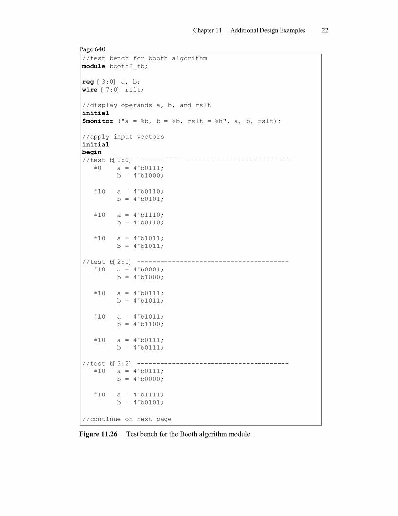
Page 640//test bench for booth algorithmmodule booth2_tb;
reg [3:0] a, b;wire [7:0] rslt;
//display operands a, b, and rsltinitial$monitor ("a = %b, b = %b, rslt = %h", a, b, rslt);
//apply input vectorsinitialbegin//test b[1:0] ----------------------------------------
#0 a = 4'b0111;b = 4'b1000;
#10 a = 4'b0110;b = 4'b0101;
#10 a = 4'b1110;b = 4'b0110;
#10 a = 4'b1011;b = 4'b1011;
//test b[2:1] ---------------------------------------#10 a = 4'b0001;
b = 4'b1000;
#10 a = 4'b0111;b = 4'b1011;
#10 a = 4'b1011;b = 4'b1100;
#10 a = 4'b0111;b = 4'b0111;
//test b[3:2] ---------------------------------------#10 a = 4'b0111;
b = 4'b0000;
#10 a = 4'b1111;b = 4'b0101;
//continue on next page
Figure 11.26 Test bench for the Booth algorithm module.

Chapter 11 Additional Design Examples 23
#10 a = 4'b0101;b = 4'b1010;
#10 a = 4'b1101;b = 4'b1100;
#10 $stop;end
//instantiate the module into the test benchbooth2 inst1 (
.a(a),
.b(b),
.rslt(rslt));
endmodule
Figure 11.26 (Continued)
a = 0111, b = 1000, rslt = c8a = 0110, b = 0101, rslt = 1ea = 1110, b = 0110, rslt = f4a = 1011, b = 1011, rslt = 19a = 0001, b = 1000, rslt = f8a = 0111, b = 1011, rslt = dd
a = 1011, b = 1100, rslt = 14a = 0111, b = 0111, rslt = 31a = 0111, b = 0000, rslt = 00a = 1111, b = 0101, rslt = fba = 0101, b = 1010, rslt = e2a = 1101, b = 1100, rslt = 0c
Figure 11.27 Outputs for the Booth algorithm module of Figure 11.25.
Figure 11.28 Waveforms for the Booth algorithm module of Figure 11.25.

Chapter 11 Additional Design Examples 24
Page 642
b1 0 1
c0 1 1
dz1
0 0 0
a
y1 y2 y3 0 0 1
ez2
1 1 1
z1↑t1↓t3 z2 ↑t1↓t
x1
x1'
x1' x1'
x1 x1
Figure 11.29 State diagram for the Moore machine of Section 11.6.
Page 643
//structural Moore ssmmodule moore_ssm8 (x1, clk, set1_n, set2_n, set3_n, rst1_n,
rst2_n, rst3_n, y, y_n, z1, z2);
input x1, clk;input set1_n, set2_n, set3_n;input rst1_n, rst2_n, rst3_n;output [1:3] y, y_n;output z1, z2;
//continued on next page
Figure 11.32 Structural module for the Moore machine of Figure 11.31.

Chapter 11 Additional Design Examples 25
wire x1, clk;wire set1_n, set2_n, set3_n;wire rst1_n, rst2_n, rst3_n;wire net1, net2, net3, net5, net6, net7, net9, net10, net11;wire [1:3] y, y_n;wire z1, z2;
//instantiate the input logic for flip-flop y[1] -----------and3_df inst1 (
.x1(y_n[2]),
.x2(y[3]),
.x3(~x1),
.z1(net1));
and3_df inst2 (.x1(y_n[1]),.x2(y[2]),.x3(x1),.z1(net2));
or2_df inst3 (.x1(net1),.x2(net2),.z1(net3));
d_ff inst4 (.d(net3),.clk(clk),.q(y[1]),.q_n(y_n[1]),.set_n(set1_n),.rst_n(rst1_n));
//instantiate the input logic for flip-flop y[2] -----------and3_df inst5 (
.x1(y_n[1]),
.x2(y[3]),
.x3(x1),
.z1(net5));
//continued on next page
Figure 11.32 (Continued)

Chapter 11 Additional Design Examples 26
and3_df inst6 (.x1(y[1]),.x2(y_n[2]),.x3(~x1),.z1(net6));
or2_df inst7 (.x1(net5),.x2(net6),.z1(net7));
d_ff inst8 (.d(net7),.clk(clk),.q(y[2]),.q_n(y_n[2]),.set_n(set2_n),.rst_n(rst2_n));
//instantiate the input logic for flip-flop y[3] -----------xor2_df inst9 (
.x1(y[1]),
.x2(x1),
.z1(net9));
xnor2_df inst10 (.x1(y[1]),.x2(y[2]),.z1(net10));
or2_df inst11 (.x1(net9),.x2(net10),.z1(net11));
//continued on next page
Figure 11.32 (Continued)

Chapter 11 Additional Design Examples 27
d_ff inst12 (.d(net11),.clk(clk),.q(y[3]),.q_n(y_n[3]),.set_n(set3_n),.rst_n(rst3_n));
//instantiate the logic for outputs z1 and z2 -----------and3_df inst13 (
.x1(y_n[1]),
.x2(y_n[2]),
.x3(y_n[3]),
.z1(z1));
and3_df inst14 (.x1(y[1]),.x2(y[2]),.x3(y[3]),.z1(z2));
endmodule
Figure 11.32 (Continued)
Page 646
//test bench for Moore ssmmodule moore_ssm8_tb;
reg x1, clk;reg set1_n, set2_n, set3_n;reg rst1_n, rst2_n, rst3_n;wire [1:3] y, y_n;wire z1, z2;
initial //display inputs and outputs$monitor ("x1 = %b, state = %b, z1z2 = %b", x1, y, {z1, z2});
//continued on next page
Figure 11.33 Test bench for the Moore machine of Figure 11.31.

Chapter 11 Additional Design Examples 28
//define clockinitialbegin
clk = 1'b0;forever
#10 clk = ~clk;end
//define input sequenceinitialbegin
#0 set1_n = 1'b1;set2_n = 1'b1;set3_n = 1'b0;
rst1_n = 1'b0;rst2_n = 1'b0;rst3_n = 1'b1;x1 = 1'b0;
#5 set1_n = 1'b1;set2_n = 1'b1;set3_n = 1'b1;
rst1_n = 1'b1;rst2_n = 1'b1;rst3_n = 1'b1;
x1 = 1'b0;@ (posedge clk) //go to state_b (101)
x1 = 1'b1;@ (posedge clk) //go to state_d (000)
//and assert z1 (t1 -- t3)
x1 = 1'b0;@ (posedge clk) //go to state_a (001)
x1 = 1'b1;@ (posedge clk) //go to state_c (011)
x1 = 1'b1;@ (posedge clk) //go to state_e (111)
//and assert z2 (t1 -- t3)
//continued on next page
Figure 11.33 (Continued)

Chapter 11 Additional Design Examples 29
x1 = 1'b0;@ (posedge clk) //go to state_a (001)
x1 = 1'b0;@ (posedge clk) //go to state_b (101)
x1 = 1'b0;@ (posedge clk) //go to state_e (111)
//and assert z2 (t1 -- t3)
x1 = 1'b0;@ (posedge clk) //go to state_a (001)
x1 = 1'b1;@ (posedge clk) //go to state_c (011)
x1 = 1'b0;@ (posedge clk) //go to state_d (000)
//and assert z1 (t1 -- t3)
x1 = 1'b0;@ (posedge clk) //go to state_a (001)
#10 $stop;
end
//instantiate the module into the test benchmoore_ssm8 inst1 (
.x1(x1),
.clk(clk),
.set1_n(set1_n),
.set2_n(set2_n),
.set3_n(set3_n),
.rst1_n(rst1_n),
.rst2_n(rst2_n),
.rst3_n(rst3_n),
.y(y),
.y_n(y_n),
.z1(z1),
.z2(z2));
endmodule
Figure 11.33 (Continued)
Chapter 11 Additional Design Examples 30
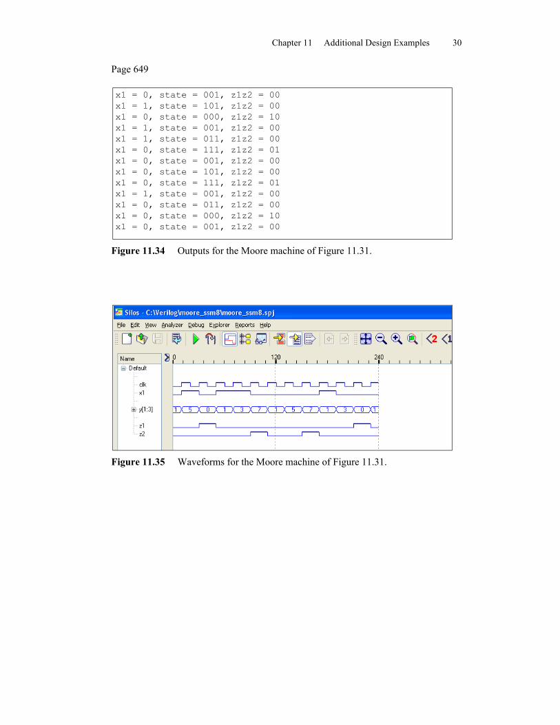
Page 649
x1 = 0, state = 001, z1z2 = 00x1 = 1, state = 101, z1z2 = 00x1 = 0, state = 000, z1z2 = 10x1 = 1, state = 001, z1z2 = 00x1 = 1, state = 011, z1z2 = 00x1 = 0, state = 111, z1z2 = 01x1 = 0, state = 001, z1z2 = 00x1 = 0, state = 101, z1z2 = 00x1 = 0, state = 111, z1z2 = 01x1 = 1, state = 001, z1z2 = 00x1 = 0, state = 011, z1z2 = 00x1 = 0, state = 000, z1z2 = 10x1 = 0, state = 001, z1z2 = 00
Figure 11.34 Outputs for the Moore machine of Figure 11.31.
Figure 11.35 Waveforms for the Moore machine of Figure 11.31.

Chapter 11 Additional Design Examples 31
Page 650
a
y1 y2 0 0
z1
b0 1
c1 0
x1x2
x2
x1
x1
x2
Figure 11.36 State diagram for the Mealy pulse-mode machine of Section 11.7.
//structural Mealy pulse-mode asynchronous sequential machinemodule pm_asm_mealy (set_n, rst_n, x1, x2, y1, y2, z1);
input set_n, rst_n;input x1, x2;output y1, y2;output z1;
//continued on next page
Page 652
Figure 11.40 Structural module for the Mealy pulse-mode machine of Figure 11.39.

Chapter 11 Additional Design Examples 32
//define internal netswire net1, net2, net3, net4, net5, net6, net8, net9;
//design for clock input -------------------------nor2_df inst1 (
.x1(x1),
.x2(x2),
.z1(net1));
//design for latch Ly1 ---------------------------nand2_df inst2 (
.x1(y2),
.x2(x2),
.z1(net2));
and2_df inst3 (.x1(y1),.x2(x2),.z1(net3));
nor2_df inst4 (.x1(x1),.x2(net3),.z1(net4));
nand2_df inst5 (.x1(net2),.x2(net6),.z1(net5));
nand3_df inst6 (.x1(net5),.x2(net4),.x3(rst_n),.z1(net6));
//continued on next page
Figure 11.40 (Continued)

Chapter 11 Additional Design Examples 33
//design for D flip-flop y1 -----------------------d_ff inst7 (
.d(net5),
.clk(net1),
.q(y1),
.q_n(),
.set_n(set_n),
.rst_n(rst_n));
//design for latch Ly2 ----------------------------nand2_df inst8 (
.x1(~x1),
.x2(net9),
.z1(net8));
nand3_df inst9 (.x1(net8),.x2(~x2),.x3(rst_n),.z1(net9));
//design for D flip-flop y2 -----------------------d_ff inst10 (
.d(net8),
.clk(net1),
.q(y2),
.q_n(),
.set_n(set_n),
.rst_n(rst_n));
//design for output z1 ----------------------------and2_df inst11 (
.x1(y1),
.x2(x2),
.z1(z1));
endmodule
Figure 11.40 (Continued)

Chapter 11 Additional Design Examples 34
Page 655
//test bench for the Mealy pulse-mode machinemodule pm_asm_mealy_tb;
reg x1, x2;reg set_n, rst_n;wire y1, y2;wire z1;
//display variablesinitial$monitor ("x1x2=%b, state=%b, z1=%b", {x1, x2}, {y1, y2}, z1);
//define input sequenceinitialbegin
#0 set_n = 1'b1;rst_n = 1'b0; //reset to state_a(00)x1 = 1'b0;x2 = 1'b0;
#5 rst_n = 1'b1; //deassert reset
#10 x1=1'b1; x2=1'b0; //go to state_b(01)#10 x1=1'b0; x2=1'b0;#10 x1=1'b0; x2=1'b1; //go to state_c(10)#10 x1=1'b0; x2=1'b0;#10 x1=1'b0; x2=1'b1; //assert z1; go to state_a(00)#10 x1=1'b0; x2=1'b0;#10 x1=1'b0; x2=1'b1; //go to state_a(00)#10 x1=1'b0; x2=1'b0;#10 x1=1'b1; x2=1'b0; //go to state_b(01)#10 x1=1'b0; x2=1'b0;#10 x1=1'b1; x2=1'b0; //go to state_b(01)#10 x1=1'b0; x2=1'b0;#10 x1=1'b0; x2=1'b1; //go to state_c(10)#10 x1=1'b0; x2=1'b0;#10 x1=1'b0; x2=1'b1; //assert z1; go to state_a(00)#10 x1=1'b0; x2=1'b0;#10 x1=1'b0; x2=1'b1; //go to state_a(00)#10 x1=1'b0; x2=1'b0;
#10 $stop;end
//continued on next page
Figure 11.41 Test bench for the Mealy pulse-mode machine of Figure 11.39.
Chapter 11 Additional Design Examples 35
//instantiate the module into the test benchpm_asm_mealy inst1 (
.set_n(set_n),
.rst_n(rst_n),
.x1(x1),
.x2(x2),
.y1(y1),
.y2(y2),
.z1(z1));
endmodule
Figure 11.41 (Continued)
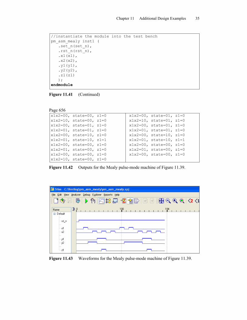
Page 656x1x2=00, state=00, z1=0x1x2=10, state=00, z1=0x1x2=00, state=01, z1=0x1x2=01, state=01, z1=0x1x2=00, state=10, z1=0x1x2=01, state=10, z1=1x1x2=00, state=00, z1=0x1x2=01, state=00, z1=0x1x2=00, state=00, z1=0x1x2=10, state=00, z1=0
x1x2=00, state=01, z1=0x1x2=10, state=01, z1=0x1x2=00, state=01, z1=0x1x2=01, state=01, z1=0x1x2=00, state=10, z1=0x1x2=01, state=10, z1=1x1x2=00, state=00, z1=0x1x2=01, state=00, z1=0x1x2=00, state=00, z1=0
Figure 11.42 Outputs for the Mealy pulse-mode machine of Figure 11.39.
Figure 11.43 Waveforms for the Mealy pulse-mode machine of Figure 11.39.

Chapter 11 Additional Design Examples 36
Page 657
a
y1 y2 y31 0 0
z1
b0 1 0
c0 0 1
x1
x1'
x1'x1
x1'x1
z1
Figure 11.44 State diagram for the Mealy one-hot machine of Section 11.8.
Page 659
//structural module for a Mealy one-hot machinemodule mealy_one_hot_struc (set_n_y1, set_n_y2y3, rst_n_y1,
rst_n_y2y3, clk, x1, y1, y1_n,y2, y2_n, y3, y3_n, z1);
input set_n_y1, set_n_y2y3, rst_n_y1, rst_n_y2y3, clk, x1;output y1, y1_n, y2, y2_n, y3, y3_n, z1;
//continued on next page
Figure 11.47 Structural module for the Mealy one-hot machine of Figure 11.46.

Chapter 11 Additional Design Examples 37
//define internal netswire net1, net2, net3, net5, net6, net7, net9, net10, net11;
//design the logic for flip-flop y1and2_df inst1 (
.x1(y3),
.x2(x1),
.z1(net1));
and2_df inst2 (.x1(y1),.x2(~x1),.z1(net2));
or2_df inst3 (.x1(net1),.x2(net2),.z1(net3));
d_ff inst4 (.d(net3),.clk(clk),.q(y1),.q_n(y1_n),.set_n(set_n_y1),.rst_n(rst_n_y1));
//design the logic for flip-flop y2and2_df inst5 (
.x1(y2),
.x2(~x1),
.z1(net5));
and2_df inst6 (.x1(y1),.x2(x1),.z1(net6));
//continued on next page
Figure 11.47 (Continued)

Chapter 11 Additional Design Examples 38
or2_df inst7 (.x1(net5),.x2(net6),.z1(net7));
d_ff inst8 (.d(net7),.clk(clk),.q(y2),.q_n(y2_n),.set_n(set_n_y2y3),.rst_n(rst_n_y2y3));
//design the logic for flip-flop y3and2_df inst9 (
.x1(y3),
.x2(~x1),
.z1(net9));
and2_df inst10 (.x1(y2),.x2(x1),.z1(net10));
or2_df inst11 (.x1(net9),.x2(net10),.z1(net11));
d_ff inst12 (.d(net11),.clk(clk),.q(y3),.q_n(y3_n),.set_n(set_n_y2y3),.rst_n(rst_n_y2y3));
//continued on next page
Figure 11.47 (Continued)

Chapter 11 Additional Design Examples 39
//design the logic for output z1and2_df inst13 (
.x1(y2_n),
.x2(x1),
.z1(z1));
endmodule
Figure 11.47 (Continued)
Page 662//test bench for the Mealy one-hot machinemodule mealy_one_hot_struc_tb;
reg set_n_y1, set_n_y2y3, rst_n_y1, rst_n_y2y3, clk, x1;wire y1, y1_n, y2, y2_n, y3, y3_n, z1;
//display variablesinitial$monitor ("x1=%b, y1 y2 y3=%b, z1=%b", x1, {y1, y2, y3}, z1);
//define clockinitialbegin
clk = 1'b0;forever
#10clk = ~clk;end
//define input sequenceinitialbegin
#0 set_n_y1 = 1'b0;rst_n_y1 = 1'b1;set_n_y2y3 = 1'b1;rst_n_y2y3 = 1'b0;x1 = 1'b0;
#10 rst_n_y2y3 = 1'b1;set_n_y1 = 1'b1;
x1 = 1'b1; //assert z1@ (posedge clk) //and go to state 010
//continued on next page
Figure 11.48 Test bench for the Mealy one-hot machine of Figure 11.46.

Chapter 11 Additional Design Examples 40
x1 = 1'b1;@ (posedge clk) //go to state 001
x1 = 1'b1; //assert z1@ (posedge clk) //and go to state 100
x1 = 1'b0;@ (posedge clk) //remain in state 100
x1 = 1'b1; //assert z1@ (posedge clk) //and go to state 010
x1 = 1'b0;@ (posedge clk) //remain in state 010
x1 = 1'b1;@ (posedge clk) //go to state 001
x1 = 1'b0;@ (posedge clk) //remain in state 001
x1 = 1'b1; //assert z1@ (posedge clk) //and go to state 100
x1 = 1'b0;@ (posedge clk) //remain in state 100
#10 $stop;end
//instantiate the module into the test benchmealy_one_hot_struc inst1 (
.set_n_y1(set_n_y1),
.set_n_y2y3(set_n_y2y3),
.rst_n_y1(rst_n_y1),
.rst_n_y2y3(rst_n_y2y3),
.clk(clk),
.x1(x1),
.y1(y1),
.y1_n(y1_n),
.y2(y2),
.y2_n(y2_n),
.y3(y3),
.y3_n(y3_n),
.z1(z1));
endmodule
Figure 11.48 (Continued)

Chapter 11 Additional Design Examples 41
Page 664
x1=0, y1 y2 y3=100, z1=0x1=1, y1 y2 y3=100, z1=1x1=1, y1 y2 y3=010, z1=0x1=0, y1 y2 y3=001, z1=0x1=1, y1 y2 y3=001, z1=1x1=0, y1 y2 y3=100, z1=0x1=1, y1 y2 y3=100, z1=1x1=0, y1 y2 y3=010, z1=0x1=1, y1 y2 y3=010, z1=0x1=0, y1 y2 y3=001, z1=0
Figure 11.49 Outputs for the Mealy one-hot machine of Figure 11.46.
Figure 11.50 Waveforms for the Mealy one-hot machine of Figure 11.46.

Chapter 11 Additional Design Examples 42
Page 665
a
y1 y2 y31 0 0
z1
b0 1 0
c0 0 1
z1
x1
x1'
x1'x1
x1'x1
Figure 11.51 State diagram for a Mealy one-hot sequential machine.
//behavioral mealy one-hot state machinemodule mealy_one_hot2 (clk, rst_n, x1, state, z1);
input clk, rst_n, x1;output z1;output [2:0] state;
wire clk, rst_n, x1;reg z1;reg [2:0] state;
//continued on next page
Figure 11.52 Behavioral module for the Mealy one-hot machine of Figure 11.51.
Chapter 11 Additional Design Examples 43
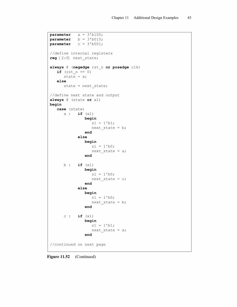
parameter a = 3'b100;parameter b = 3'b010;parameter c = 3'b001;
//define internal registersreg [2:0] next_state;
always @ (negedge rst_n or posedge clk)if (rst_n == 0)
state = a;else
state = next_state;
//define next state and outputalways @ (state or x1)begin
case (state)a : if (x1)
beginz1 = 1'b1;next_state = b;
endelse
beginz1 = 1'b0;next_state = a;
end
b : if (x1)begin
z1 = 1'b0;next_state = c;
endelse
beginz1 = 1'b0;next_state = b;
end
c : if (x1)begin
z1 = 1'b1;next_state = a;
end
//continued on next page
Figure 11.52 (Continued)

Chapter 11 Additional Design Examples 44
elsebegin
z1 = 1'b0;next_state = c;
enddefault: begin
next_state = a;z1 = 1'b0;
endendcase
end
endmodule
Figure 11.52 (Continued)
//test bench for the Mealy one-hot machinemodule mealy_one_hot2_tb;
reg clk, rst_n, x1;wire [2:0] state;wire z1;
//display variablesinitial$monitor ("x1 = %b, state = %b, z1 = %b", x1, state, z1);
//define clockinitialbegin
clk = 1'b0;forever
#10clk = ~clk;end
//define input sequenceinitialbegin
#0 rst_n = 1'b0;x1 = 1'b0;
#10 rst_n = 1'b1;
//continued on next page
Page 667
Figure 11.53 Test bench for the Mealy one-hot machine of Figure 11.51.

Chapter 11 Additional Design Examples 45
x1 = 1'b1; //assert z1@ (posedge clk) //and go to state_b (010)
x1 = 1'b1;@ (posedge clk) //go to state_c (001)
x1 = 1'b1; //assert z1@ (posedge clk) //and go to state_a (100)
x1 = 1'b0;@ (posedge clk) //remain in state_a (100)
x1 = 1'b1; //assert z1@ (posedge clk) //and go to state_b (010)
x1 = 1'b0;@ (posedge clk) //remain in state_b (010)
x1 = 1'b1;@ (posedge clk) //go to state_c (001)
x1 = 1'b0;@ (posedge clk) //remain in state_c (001)
x1 = 1'b1; //assert z1@ (posedge clk) //and go to state_a (100)
x1 = 1'b0;@ (posedge clk) //remain in state_a (100)
#10 $stop;end
//instantiate the module into the test benchmealy_one_hot2 inst1 (
.clk(clk),
.rst_n(rst_n),
.x1(x1),
.state(state),
.z1(z1));
endmodule
Figure 11.53 (Continued)

Chapter 11 Additional Design Examples 46
Page 669
x1 = 0, state = 100, z1 = 0x1 = 1, state = 010, z1 = 0x1 = 1, state = 001, z1 = 1x1 = 0, state = 100, z1 = 0x1 = 1, state = 100, z1 = 1x1 = 0, state = 010, z1 = 0x1 = 1, state = 010, z1 = 0x1 = 0, state = 001, z1 = 0x1 = 1, state = 001, z1 = 1x1 = 0, state = 100, z1 = 0
Figure 11.54 Outputs for the Mealy one-hot machine of Figure 11.51.
Figure 11.55 Waveforms for the Mealy one-hot machine of Figure 11.51.

Chapter 11 Additional Design Examples 47
Page 676//mixed-design module for 9s complementermodule nines_compl (m, b, f);
input m;input [3:0] b;output [3:0] f;
//define internal netswire net2, net3, net4, net6, net7;
//instantiate the logic gates for the 9s complementerxor2_df inst1 (
.x1(b[0]),
.x2(m),
.z1(f[0]));
assign f[1] = b[1];
and2_df inst2 (.x1(~m),.x2(b[2]),.z1(net2));
xor2_df inst3 (.x1(b[2]),.x2(b[1]),.z1(net3));
and2_df inst4 (.x1(net3),.x2(m),.z1(net4));
or2_df inst5 (.x1(net2),.x2(net4),.z1(f[2]));
//continued on next page
Figure 11.59 Structural module for a 9s complementer.

Chapter 11 Additional Design Examples 48
and2_df inst6 (.x1(~m),.x2(b[3]),.z1(net6));
and4_df inst7 (.x1(m),.x2(~b[3]),.x3(~b[2]),.x4(~b[1]),.z1(net7));
or2_df inst8 (.x1(net6),.x2(net7),.z1(f[3]));
endmodule
Figure 11.59 (Continued)
Page 677//test bench for 9s complementermodule nines_compl_tb;
reg m;reg [3:0] b;wire [3:0] f;
//display variablesinitial$monitor ("m=%b, b=%b, f=%b", m, b, f);
//apply input vectorsinitialbegin//add -- do not complement
#0 m = 1'b0; b = 4'b0000;#10 m = 1'b0; b = 4'b0001;#10 m = 1'b0; b = 4'b0010;#10 m = 1'b0; b = 4'b0011;
//continued on next page
Figure 11.60 Test bench for the 9s complementer of Figure 11.59.

Chapter 11 Additional Design Examples 49
#10 m = 1'b0; b = 4'b0100;#10 m = 1'b0; b = 4'b0101;#10 m = 1'b0; b = 4'b0110;#10 m = 1'b0; b = 4'b0111;#10 m = 1'b0; b = 4'b1000;#10 m = 1'b0; b = 4'b1001;
//subtract -- complement#10 m = 1'b1; b = 4'b0000;#10 m = 1'b1; b = 4'b0001;#10 m = 1'b1; b = 4'b0010;#10 m = 1'b1; b = 4'b0011;#10 m = 1'b1; b = 4'b0100;#10 m = 1'b1; b = 4'b0101;#10 m = 1'b1; b = 4'b0110;#10 m = 1'b1; b = 4'b0111;#10 m = 1'b1; b = 4'b1000;#10 m = 1'b1; b = 4'b1001;
#10 $stop;end
//instantiate the module into the test benchnines_compl inst1 (
.m(m),
.b(b),
.f(f));
endmodule
Figure 11.60 (Continued)
Page 678Addm=0, b=0000, f=0000m=0, b=0001, f=0001m=0, b=0010, f=0010m=0, b=0011, f=0011m=0, b=0100, f=0100m=0, b=0101, f=0101m=0, b=0110, f=0110m=0, b=0111, f=0111m=0, b=1000, f=1000m=0, b=1001, f=1001
Subtractm=1, b=0000, f=1001m=1, b=0001, f=1000m=1, b=0010, f=0111m=1, b=0011, f=0110m=1, b=0100, f=0101m=1, b=0101, f=0100m=1, b=0110, f=0011m=1, b=0111, f=0010m=1, b=1000, f=0001m=1, b=1001, f=0000
Figure 11.61 Outputs for the 9s complementer of Figure 11.59.

Chapter 11 Additional Design Examples 50
Page 681//structural bcd adder subtractormodule add_sub_bcd (a, b, m, bcd, cout);
input [7:0] a, b;input m;output [7:0] bcd;output cout;
//define internal netswire [7:0] f;wire [7:0] sum;wire cout3, aux_cy, cout7;wire net3, net4, net9, net10;
//instantiate the logic for the low-order stage [3:0]//instantiate the 9s complementernines_compl inst1 (
.m(m),
.b(b[3:0]),
.f(f[3:0]));
//instantiate the adder for the intermediate sumadder4 inst2 (
.a(a[3:0]),
.b(f[3:0]),
.cin(m),
.sum(sum[3:0]),
.cout(cout3));
//instantiate the logic gatesand2_df inst3 (
.x1(sum[3]),
.x2(sum[1]),
.z1(net3));
and2_df inst4 (.x1(sum[2]),.x2(sum[3]),.z1(net4));
//continued on next page
Figure 11.63 Structural module for the BCD adder/subtractor of Figure 11.62.

Chapter 11 Additional Design Examples 51
or3_df inst5 (.x1(cout3),.x2(net3),.x3(net4),.z1(aux_cy));
//instantiate the adder for the bcd sum [3:0]adder4 inst6 (
.a(sum[3:0]),
.b({1'b0, aux_cy, aux_cy, 1'b0}),
.cin(1'b0),
.sum(bcd[3:0]));
//instantiate the logic for the high-order stage [7:4]//instantiate the 9s complementernines_compl inst7 (
.m(m),
.b(b[7:4]),
.f(f[7:4]));
//instantiate the adder for the intermediate sumadder4 inst8 (
.a(a[7:4]),
.b(f[7:4]),
.cin(aux_cy),
.sum(sum[7:4]),
.cout(cout7));
//instantiate the logic gatesand2_df inst9 (
.x1(sum[7]),
.x2(sum[5]),
.z1(net9));
and2_df inst10 (.x1(sum[6]),.x2(sum[7]),.z1(net10));
//continued on next page
Figure 11.63 (Continued)

Chapter 11 Additional Design Examples 52
or3_df inst11 (.x1(cout7),.x2(net9),.x3(net10),.z1(cout));
//instantiate the adder for the bcd sum [7:0]adder4 inst12 (
.a(sum[7:4]),
.b({1'b0, cout, cout, 1'b0}),
.cin(1'b0),
.sum(bcd[7:4]));
endmodule
Figure 11.63 (Continued)
Page 683
//test bench for the bcd adder subtractormodule add_sub_bcd_tb;
reg [7:0] a, b;reg m;
wire [7:0] bcd;wire cout;
//display variablesinitial$monitor ("a=%b, b=%b, m=%b, cout=%b, bcd=%b",
a, b, m, cout, bcd);
//apply input vectorsinitialbegin//add bcd
#0 a = 8'b1001_1001; b = 8'b0110_0110; m = 1'b0;#10 a = 8'b0010_0110; b = 8'b0101_1001; m = 1'b0;#10 a = 8'b0001_0001; b = 8'b0011_0011; m = 1'b0;
//continued on next page
Figure 11.64 Test bench for the BCD adder/subtractor of Figure 11.63.
Chapter 11 Additional Design Examples 53
#10 a = 8'b0000_1000; b = 8'b0000_0101; m = 1'b0;#10 a = 8'b0110_1000; b = 8'b0011_0101; m = 1'b0;#10 a = 8'b1000_1001; b = 8'b0101_1001; m = 1'b0;#10 a = 8'b1001_0110; b = 8'b1001_0011; m = 1'b0;#10 a = 8'b1001_1001; b = 8'b0000_0001; m = 1'b0;#10 a = 8'b1001_1001; b = 8'b0110_0110; m = 1'b0;
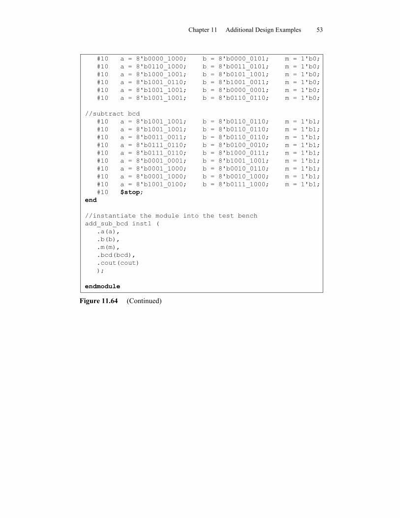
//subtract bcd#10 a = 8'b1001_1001; b = 8'b0110_0110; m = 1'b1;#10 a = 8'b1001_1001; b = 8'b0110_0110; m = 1'b1;#10 a = 8'b0011_0011; b = 8'b0110_0110; m = 1'b1;#10 a = 8'b0111_0110; b = 8'b0100_0010; m = 1'b1;#10 a = 8'b0111_0110; b = 8'b1000_0111; m = 1'b1;#10 a = 8'b0001_0001; b = 8'b1001_1001; m = 1'b1;#10 a = 8'b0001_1000; b = 8'b0010_0110; m = 1'b1;#10 a = 8'b0001_1000; b = 8'b0010_1000; m = 1'b1;#10 a = 8'b1001_0100; b = 8'b0111_1000; m = 1'b1;#10 $stop;
end
//instantiate the module into the test benchadd_sub_bcd inst1 (
.a(a),
.b(b),
.m(m),
.bcd(bcd),
.cout(cout));
endmodule
Figure 11.64 (Continued)

Chapter 11 Additional Design Examples 54
Additiona=1001_1001, b=0110_0110, m=0, cout=1, bcd=0110_0101a=0010_0110, b=0101_1001, m=0, cout=0, bcd=1000_0101a=0001_0001, b=0011_0011, m=0, cout=0, bcd=0100_0100a=0000_1000, b=0000_0101, m=0, cout=0, bcd=0001_0011a=0110_1000, b=0011_0101, m=0, cout=1, bcd=0000_0011a=1000_1001, b=0101_1001, m=0, cout=1, bcd=0100_1000a=1001_0110, b=1001_0011, m=0, cout=1, bcd=1000_1001a=1001_1001, b=0000_0001, m=0, cout=1, bcd=0000_0000a=1001_1001, b=0110_0110, m=0, cout=1, bcd=0110_0101----------------------------------------------------Subtractiona=1001_1001, b=0110_0110, m=1, cout=1, bcd=0011_0011a=0011_0011, b=0110_0110, m=1, cout=0, bcd=0110_0111a=0111_0110, b=0100_0010, m=1, cout=1, bcd=0011_0100a=0111_0110, b=1000_0111, m=1, cout=0, bcd=1000_1001a=0001_0001, b=1001_1001, m=1, cout=0, bcd=0001_0010a=0001_1000, b=0010_0110, m=1, cout=0, bcd=1001_0010a=0001_1000, b=0010_1000, m=1, cout=0, bcd=1001_0000a=1001_0100, b=0111_1000, m=1, cout=1, bcd=0001_0110
Figure 11.65 Outputs for the BCD adder/subtractor of Figure 11.63.
Figure 11.66 Waveforms for the BCD adder/subtractor of Figure 11.63.

Chapter 11 Additional Design Examples 55
Page 690
icache iunit decode eunit dcache
0
31
0
15
ir
pc
instruction
iu_pc
13
5
decoder
clk
dcaddr
ctrl
dcaddr
opnda
dst
opndbalu
01234567
regfile
dst
rslt
4
8
eu_dcaddr
eu_dcenbl
eu_result
dc_dataout
11
4
3
3
3
3
opcode
8
8
rst_n
13iu_instr
amux
bmuxmux
du_opcodeopcode
du_dstin
du_addrin
du_opnda_addr
du_opndb_addr
4
eu_reg_wr_vld
opcode_out
>
>
>
>
> >
>
>
8>
>
>
+1
1
eu_load_op1
clkrst_n
regfile0:7_out
eu_dst
eu_rdwr
Figure 11.71 Architecture for the pipelined RISC processor of Section 11.10.

Chapter 11 Additional Design Examples 56
Page 691
icacheicache_tb
iunitiunit_tb
decodedecode_tb
euniteunit_tb
regfileregfile_tb
dcachedcache_tb
structuralsystem_top_tb
structural risc_cpu_top
structural system_top
structural risc_cpu_topclk
rst_neu_dcaddr
eu_result
eu_rdwr
structural system_top
clk rst_n
iunitiunit_tb
decodedecode_tb
euniteunit_tb
regfileregfile_tb
iu_pcdc_dataout
icache dcache
instruction
eu_dcenbl
structural risc_cpu_top
risc risc risc risc risc risc
risc risc risc risc
risc
risc
risc risc
risc
Figure 11.72 Structural block diagram for the pipelined RISC processor of Section 11.10.

Chapter 11 Additional Design Examples 57
Page 694
instruction(To iunit)
pc(From iunit)
0
31
13 instruction
risc_pc5
Figure 11.73 Instruction cache for the pipelined RISC processor.

Chapter 11 Additional Design Examples 58
Page 695
clk
rst_n
instruction
pc
(From icache)
(To icache)
(To decode)>ir
13
5
13
ir
pc>
+1
clk
rst_n
instruction
iu_pc
iu_instr
Figure 11.74 Instruction unit for the pipelined RISC processor.
Chapter 11 Additional Design Examples 59
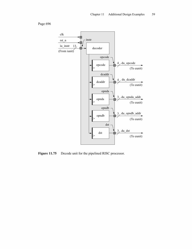
Page 696
clk
rst_n instr
(From iunit)
(To eunit)>opcode
13
4 du_opcode
decoder
(To eunit)>dcaddr 4 du_dcaddr
(To eunit)>opnda 3 du_opnda_addr
(To eunit)>opndb 3 du_opndb_addr
(To eunit)> dst 3 du_dst
iu_instr
opcode
dcaddr
opnda
opndb
dst
Figure 11.75 Decode unit for the pipelined RISC processor.

Chapter 11 Additional Design Examples 60
Page 697
clk
rst_n
>opcode4du_opcode
ctrl
(From decode)
>dcaddr4du_addrin
(From decode)3du_opnda_addr
> rslt3du_opndb_addr
> dst3du_dstin
(From decode)
(From decode)
(From decode)
alu
muxb
muxa
regfile0:7_out 8(From regfile)
opcode_out
eu_load_op1(To regfile)
eu_dcenbl
eu_rdwr
eu_reg_wr_vld
1
1
1
(To dcache:2 ports)
(To regfile)
eu_dcaddr(To dcache)
eu_result
(To dcache)(To regfile)
eu_dst(To regfile)
8
4
3
opcode
dcaddrin
(8 ports) regfile0:7
opnda_addr
opndb_addr
dstin
dcenblrdwr
reg_wr_vld
load_op
dcaddr
rslt
dst
Figure 11.76 Execution unit for the pipelined RISC processor.

Chapter 11 Additional Design Examples 61
Page 698
clk
rst_n
eu_rslt(From eunit)
8(8 ports: To eunit)
8 regfile0:7_out
eu_reg_wr_vld 1
eu_load_op 1
eu_dst 3
dcdataout 8
(From eunit)
(From eunit)
(From eunit)
(From dcache)
0
7
reg_wr_vld
load_op
dst
rslt
dcdataout
regfile0:7
Figure 11.77 Register file for the pipelined RISC processor.

Chapter 11 Additional Design Examples 62
Page 699
(To regfile)8dc_dataout
risc_dcenbl 1
risc_rdwr 1
risc_dcaddr 4
risc_rslt 8
(From eunit)
(From eunit)
(From eunit)
(From eunit)
0
15
dcdataout
dcdatain
dcenbl
rdwr
dcaddr
Figure 11.78 Data cache for the pipelined RISC processor.

Chapter 11 Additional Design Examples 63
Page 702//behavioral icache contentsmodule risc_icache (pc, instruction);
//list which are inputs and which are outputsinput [4:0] pc;output [12:0] instruction;
//list which are wire and which are regwire [4:0] pc;reg [12:0] instruction;
//define memory sizereg [12:0] icache [0:31];//# of bits per reg; # of regs
//13 bits per reg; 31 regs//icache is an array of 32 13-bit regs
//define memory contentsinitialbegin
$readmemb ("icache.instr", icache);end
/* alternatively, the icache could have been loadedby initializing each location separately as shown belowinitialbegin
icache [00] = 13'h1c00;icache [01] = 13'h1c11;icache [02] = 13'h1c22;icache [03] = 13'h1c33;icache [04] = 13'h1c44;icache [05] = 13'h1c55;icache [06] = 13'h1c66;icache [07] = 13'h1c77;icache [08] = 13'h0208;icache [09] = 13'h05f1;icache [10] = 13'h06aa;icache [11] = 13'h08e3;icache [12] = 13'h0b24;icache [13] = 13'h0d45;icache [14] = 13'h0f86;icache [15] = 13'h11c7;icache [16] = 13'h1200;icache [17] = 13'h1441;icache [18] = 13'h1682;icache [19] = 13'h18c3;icache [20] = 13'h1b04; //continued on next page
Figure 11.81 Behavioral module for the instruction cache.

Chapter 11 Additional Design Examples 64
icache [21] = 13'h1e08;icache [22] = 13'h1e19;icache [23] = 13'h1e2a;icache [24] = 13'h1e3b;icache [25] = 13'h1e4c;icache [26] = 13'h1e5d;icache [27] = 13'h1e6e;icache [28] = 13'h1e7f;icache [29] = 13'h0000;icache [30] = 13'h0000;icache [31] = 13'h0000;
end*/
always @ (pc)begin
instruction = icache [pc];endendmodule
Figure 11.81 (Continued)
Page 703//icache test benchmodule risc_icache_tb;
integer i; //used for display
reg [4:0] pc; //inputs are reg for test benchwire [12:0] instruction; //outputs are wire for test bench
initialbegin
#10 pc = 5'b00000;#10 pc = 5'b00000;#10 pc = 5'b00001;#10 pc = 5'b00010;#10 pc = 5'b00011;#10 pc = 5'b00100;#10 pc = 5'b00101;#10 pc = 5'b00110;#10 pc = 5'b00111;#10 pc = 5'b01000;#10 pc = 5'b01001;
//continued on next page
Figure 11.82 Test bench for the instruction cache.

Chapter 11 Additional Design Examples 65
#10 pc = 5'b01010;#10 pc = 5'b01011;#10 pc = 5'b01100;#10 pc = 5'b01101;#10 pc = 5'b01110;#10 pc = 5'b01111;#10 pc = 5'b10000;#10 pc = 5'b10001;#10 pc = 5'b10010;#10 pc = 5'b10011;#10 pc = 5'b10100;#10 pc = 5'b10101;#10 pc = 5'b10110;#10 pc = 5'b10111;#10 pc = 5'b11000;#10 pc = 5'b11001;#10 pc = 5'b11010;#10 pc = 5'b11011;#10 pc = 5'b11100;#10 pc = 5'b11101;#10 pc = 5'b11110;#10 pc = 5'b11111;
#20 $stop; //must not stop before display endsend //otherwise not all addrs will display
initialbegin//#20 synchs waveforms produced by the first initial with//the display produced by the second initial
#20 for (i=0; i<32; i=i+1)begin
#10 $display ("address %h = %h", i, instruction); end
#600 $stop;end
//instantiate the behavioral module into the test benchrisc_icache inst1 (
.pc(pc),
.instruction(instruction));
endmodule
Figure 11.82 (Continued)
Chapter 11 Additional Design Examples 66
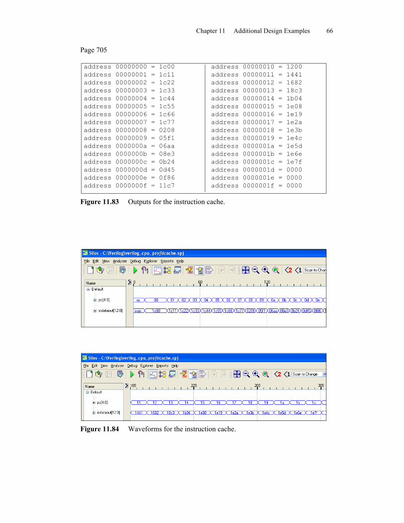
Page 705
address 00000000 = 1c00address 00000001 = 1c11address 00000002 = 1c22address 00000003 = 1c33address 00000004 = 1c44address 00000005 = 1c55address 00000006 = 1c66address 00000007 = 1c77address 00000008 = 0208address 00000009 = 05f1address 0000000a = 06aaaddress 0000000b = 08e3address 0000000c = 0b24address 0000000d = 0d45address 0000000e = 0f86address 0000000f = 11c7
address 00000010 = 1200address 00000011 = 1441address 00000012 = 1682address 00000013 = 18c3address 00000014 = 1b04address 00000015 = 1e08address 00000016 = 1e19address 00000017 = 1e2aaddress 00000018 = 1e3baddress 00000019 = 1e4caddress 0000001a = 1e5daddress 0000001b = 1e6eaddress 0000001c = 1e7faddress 0000001d = 0000address 0000001e = 0000address 0000001f = 0000
Figure 11.83 Outputs for the instruction cache.
Figure 11.84 Waveforms for the instruction cache.

Chapter 11 Additional Design Examples 67
Page 706
//behavioral iunitmodule risc_iunit (instruction, pc, ir, clk, rst_n);
//list which are inputs and which are outputsinput [12:0] instruction;input clk, rst_n;output [4:0] pc;output [12:0] ir;
//list which are wire and which are regwire [12:0] instruction;wire clk, rst_n;reg [4:0] pc, next_pc;reg [12:0] ir;
parameter nop = 13'h0000;
always @ (posedge clk or negedge rst_n)begin //must have always for each reg
if (rst_n == 1'b0) //== means comparepc = 5'b00000; //initialize pc = 00000
elsepc <= pc + 1; //determine next pc
end
always @ (posedge clk or negedge rst_n)begin
if (rst_n == 1'b0)ir = nop;
elseir <= instruction; //load ir from instruction
end
endmodule
Figure 11.85 Behavioral module for the instruction unit.

Chapter 11 Additional Design Examples 68
//test bench for iunitmodule risc_iunit_tb;
//list input and output portsreg [12:0] instruction; //inputs are reg for test benchreg clk, rst_n;wire [4:0] pc; //outputs are wire for test benchwire [12:0] ir, instr;
//define clockinitialbegin
clk = 1'b0;forever
#10 clk = ~clk;end
//define reset and simulation duration//define instructioninitialbegin
#0 rst_n = 1'b0;instruction = 13'h0208; //pc = 00$display ("pc = %h, instruction = %h, ir = %h",
pc, instruction, ir);
#5 rst_n = 1'b1;
#10 instruction = 13'h05f1; //pc = 01; sub$display ("pc = %h, instruction = %h, ir = %h",
pc, instruction, ir);
#20 instruction = 13'h06aa; //pc = 02; and$display ("pc = %h, instruction = %h, ir = %h",
pc, instruction, ir);
#20 instruction = 13'h08e3; //pc = 03; or$display ("pc = %h, instruction = %h, ir = %h",
pc, instruction, ir);
#20 instruction = 13'h0b24; //pc = 04; xor$display ("pc = %h, instruction = %h, ir = %h",
pc, instruction, ir);
#20 instruction = 13'h0d45; //pc = 05; inc$display ("pc = %h, instruction = %h, ir = %h",
pc, instruction, ir); //next page
Page 707
Figure 11.86 Test bench for the instruction unit.
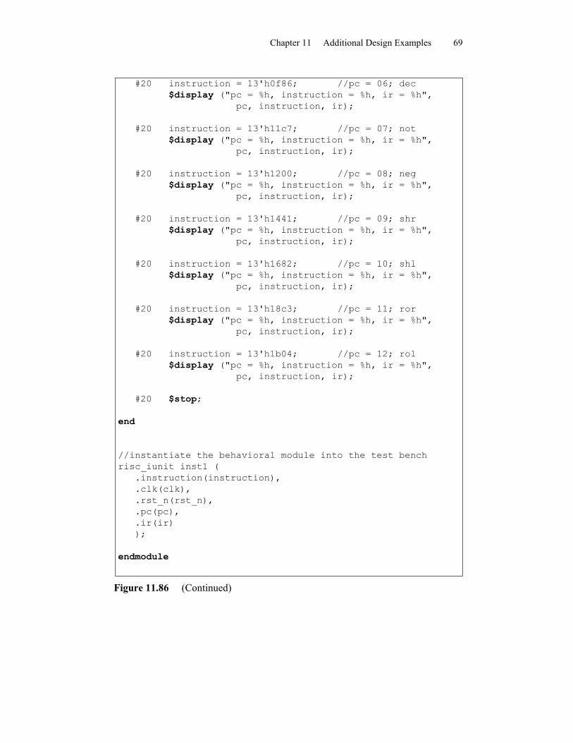
Chapter 11 Additional Design Examples 69
#20 instruction = 13'h0f86; //pc = 06; dec$display ("pc = %h, instruction = %h, ir = %h",
pc, instruction, ir);
#20 instruction = 13'h11c7; //pc = 07; not$display ("pc = %h, instruction = %h, ir = %h",
pc, instruction, ir);
#20 instruction = 13'h1200; //pc = 08; neg$display ("pc = %h, instruction = %h, ir = %h",
pc, instruction, ir);
#20 instruction = 13'h1441; //pc = 09; shr$display ("pc = %h, instruction = %h, ir = %h",
pc, instruction, ir);
#20 instruction = 13'h1682; //pc = 10; shl$display ("pc = %h, instruction = %h, ir = %h",
pc, instruction, ir);
#20 instruction = 13'h18c3; //pc = 11; ror$display ("pc = %h, instruction = %h, ir = %h",
pc, instruction, ir);
#20 instruction = 13'h1b04; //pc = 12; rol$display ("pc = %h, instruction = %h, ir = %h",
pc, instruction, ir);
#20 $stop;
end
//instantiate the behavioral module into the test benchrisc_iunit inst1 (
.instruction(instruction),
.clk(clk),
.rst_n(rst_n),
.pc(pc),
.ir(ir));
endmodule
Figure 11.86 (Continued)

Chapter 11 Additional Design Examples 70
Page 709
pc = xx, instruction = 0208, ir = xxxxpc = 01, instruction = 05f1, ir = 0208pc = 02, instruction = 06aa, ir = 05f1pc = 03, instruction = 08e3, ir = 06aapc = 04, instruction = 0b24, ir = 08e3pc = 05, instruction = 0d45, ir = 0b24pc = 06, instruction = 0f86, ir = 0d45pc = 07, instruction = 11c7, ir = 0f86pc = 08, instruction = 1200, ir = 11c7pc = 09, instruction = 1441, ir = 1200pc = 0a, instruction = 1682, ir = 1441pc = 0b, instruction = 18c3, ir = 1682pc = 0c, instruction = 1b04, ir = 18c3
Figure 11.87 Outputs for the instruction unit.
Figure 11.88 Waveforms for the instruction unit.

Chapter 11 Additional Design Examples 71
Page 710
//mixed-design decode unitmodule risc_decode (clk, rst_n, instr, dcaddr,
opnda, opndb, dst, opcode);
input clk, rst_n;input [12:0] instr;output [3:0] dcaddr, opcode;output [2:0] opnda, opndb, dst;
reg [3:0] dcaddr;reg [2:0] opnda, opndb, dst;
//define internal registers and netreg [3:0] opcode;wire [3:0] opcode_i;reg [3:0] dcaddr_i;reg [2:0] opnda_i, opndb_i, dst_i;
parameter ld = 4'b1110,st = 4'b1111;
assign opcode_i = instr[12:9];
always @ (opcode_i or instr)begin
case (opcode_i)ld: begin
dcaddr_i = instr[7:4];dst_i = instr[2:0];opnda_i = 3'b000;
end
st: begindcaddr_i = instr [3:0];dst_i = 3'b000;opnda_i = instr[6:4];opndb_i = 3'b000;
end
//continued on next page
Figure 11.89 Mixed-design module for the decode unit.

Chapter 11 Additional Design Examples 72
default: begindcaddr_i = 4'b0000;dst_i = instr [2:0];opnda_i = instr [8:6];opndb_i = instr [5:3];
endendcase
end
always @ (posedge clk or negedge rst_n)begin
if (~rst_n)begin
opcode <= 4'b0000; dcaddr <= 4'b0000; dst <= 3'b000; opnda <= 3'b000; opndb <= 3'b000;
end
elsebegin
opcode <= opcode_i; dcaddr <= dcaddr_i; dst <= dst_i;
opnda <= opnda_i;opndb <= opndb_i;
endendendmodule
Figure 11.89 (Continued)
//test bench for decode unitmodule risc_decode_tb;
reg clk, rst_n; //inputs are reg for test benchreg [12:0] instr;
wire [3:0] dcaddr; //outputs are wire for test benchwire [2:0] opnda, opndb, dst;
//continued on next page
Page 711
Figure 11.90 Test bench for the decode unit.

Chapter 11 Additional Design Examples 73
//define clockinitialbegin
clk = 1'b0;forever
#10 clk = ~clk;end
//define resetinitialbegin
#0 rst_n = 1'b0;#5 rst_n = 1'b1;
end
initialbegin
#5 instr = 13'h1c00; //ld#20 instr = 13'h0208; //add
$display ("opcode=%b, opnda=%b, opndb=%b, dst=%b",instr[12:9], opnda, opndb, dst);
#20 instr = 13'h05f1; //sub$display ("opcode=%b, opnda=%b, opndb=%b, dst=%b",
instr[12:9], opnda, opndb, dst);
#20 instr = 13'h06aa; //and$display ("opcode=%b, opnda=%b, opndb=%b, dst=%b",
instr[12:9], opnda, opndb, dst);
#20 instr = 13'h08e3; //or$display ("opcode=%b, opnda=%b, opndb=%b, dst=%b",
instr[12:9], opnda, opndb, dst);
#20 instr = 13'h0b1c; //xor$display ("opcode=%b, opnda=%b, opndb=%b, dst=%b",
instr[12:9], opnda, opndb, dst);
#20 instr = 13'h0d45; //inc$display ("opcode=%b, opnda=%b, opndb=%b, dst=%b",
instr[12:9], opnda, opndb, dst);
#20 instr = 13'h0f86; //dec$display ("opcode=%b, opnda=%b, opndb=%b, dst=%b",
instr[12:9], opnda, opndb, dst);
//continued on next page
Figure 11.90 (Continued)

Chapter 11 Additional Design Examples 74
#20 instr = 13'h11c7; //not$display ("opcode=%b, opnda=%b, opndb=%b, dst=%b",
instr[12:9], opnda, opndb, dst);
#20 instr = 13'h1200; //neg$display ("opcode=%b, opnda=%b, opndb=%b, dst=%b",
instr[12:9], opnda, opndb, dst);
#20 instr = 13'h1441; //shr$display ("opcode=%b, opnda=%b, opndb=%b, dst=%b",
instr[12:9], opnda, opndb, dst);
#20 instr = 13'h1682; //shl$display ("opcode=%b, opnda=%b, opndb=%b, dst=%b",
instr[12:9], opnda, opndb, dst);
#20 instr = 13'h18c3; //ror$display ("opcode=%b, opnda=%b, opndb=%b, dst=%b",
instr[12:9], opnda, opndb, dst);
#20 instr = 13'h1b04; //rol$display ("opcode=%b, opnda=%b, opndb=%b, dst=%b",
instr[12:9], opnda, opndb, dst);
#20 instr = 13'h1e00; //st$display ("opcode=%b, opnda=%b, opndb=%b, dst=%b",
instr[12:9], opnda, opndb, dst);
#20 $stop;
end
//instantiate the behavioral module into the test benchrisc_decode inst1 (
.clk(clk),
.rst_n(rst_n),
.instr(instr),
.dcaddr(dcaddr),
.opnda(opnda),
.opndb(opndb),
.opcode(),
.dst(dst));
endmodule
Figure 11.90 (Continued)
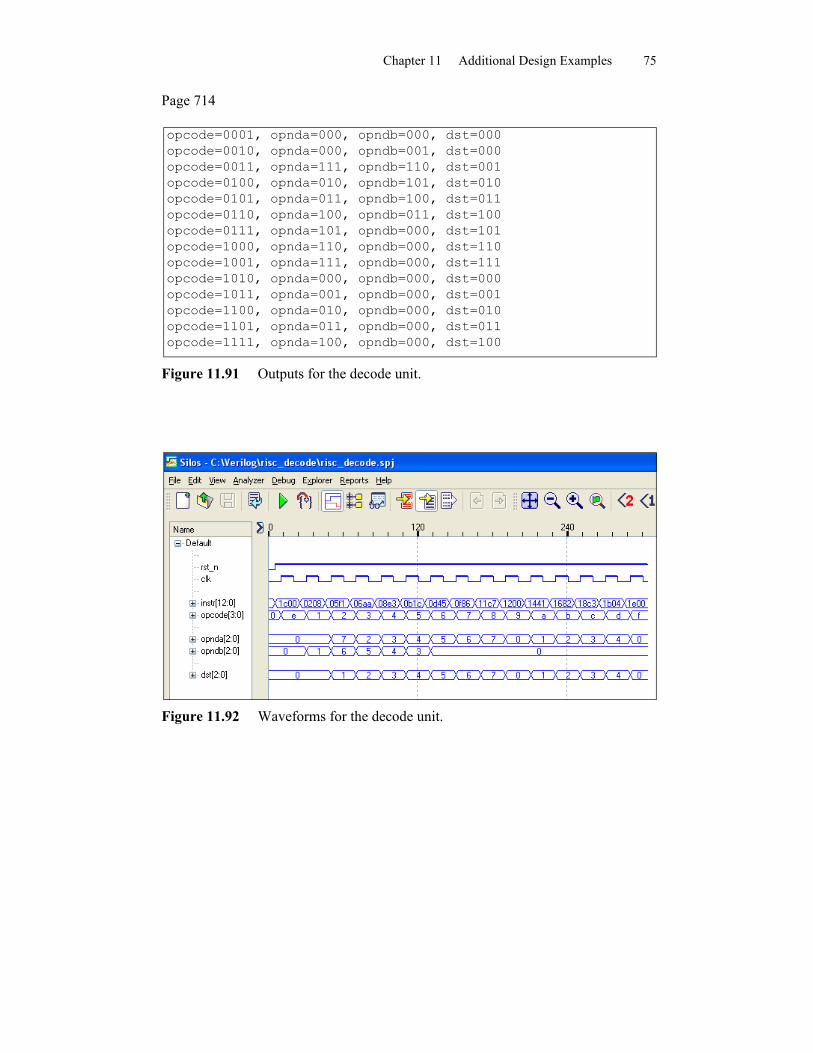
Chapter 11 Additional Design Examples 75
Page 714
opcode=0001, opnda=000, opndb=000, dst=000opcode=0010, opnda=000, opndb=001, dst=000opcode=0011, opnda=111, opndb=110, dst=001opcode=0100, opnda=010, opndb=101, dst=010opcode=0101, opnda=011, opndb=100, dst=011opcode=0110, opnda=100, opndb=011, dst=100opcode=0111, opnda=101, opndb=000, dst=101opcode=1000, opnda=110, opndb=000, dst=110opcode=1001, opnda=111, opndb=000, dst=111opcode=1010, opnda=000, opndb=000, dst=000opcode=1011, opnda=001, opndb=000, dst=001opcode=1100, opnda=010, opndb=000, dst=010opcode=1101, opnda=011, opndb=000, dst=011opcode=1111, opnda=100, opndb=000, dst=100
Figure 11.91 Outputs for the decode unit.
Figure 11.92 Waveforms for the decode unit.
Chapter 11 Additional Design Examples 76
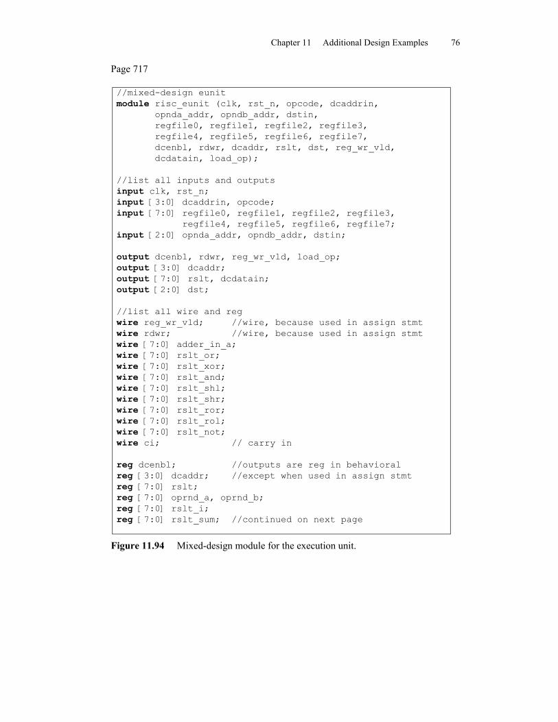
Page 717
//mixed-design eunitmodule risc_eunit (clk, rst_n, opcode, dcaddrin,
opnda_addr, opndb_addr, dstin, regfile0, regfile1, regfile2, regfile3, regfile4, regfile5, regfile6, regfile7, dcenbl, rdwr, dcaddr, rslt, dst, reg_wr_vld, dcdatain, load_op);
//list all inputs and outputsinput clk, rst_n;input [3:0] dcaddrin, opcode;input [7:0] regfile0, regfile1, regfile2, regfile3,
regfile4, regfile5, regfile6, regfile7;input [2:0] opnda_addr, opndb_addr, dstin;
output dcenbl, rdwr, reg_wr_vld, load_op;output [3:0] dcaddr;output [7:0] rslt, dcdatain;output [2:0] dst;
//list all wire and regwire reg_wr_vld; //wire, because used in assign stmtwire rdwr; //wire, because used in assign stmtwire [7:0] adder_in_a;wire [7:0] rslt_or;wire [7:0] rslt_xor;wire [7:0] rslt_and;wire [7:0] rslt_shl;wire [7:0] rslt_shr;wire [7:0] rslt_ror;wire [7:0] rslt_rol;wire [7:0] rslt_not;wire ci; // carry in
reg dcenbl; //outputs are reg in behavioralreg [3:0] dcaddr; //except when used in assign stmtreg [7:0] rslt;reg [7:0] oprnd_a, oprnd_b;reg [7:0] rslt_i;reg [7:0] rslt_sum; //continued on next page
Figure 11.94 Mixed-design module for the execution unit.

Chapter 11 Additional Design Examples 77
reg [7:0] adder_in_b;reg adder_mode;reg co; // carry out
//define internal registersreg [2:0] dst;reg [3:0] opcode_out;
parameter add = 1'b0;parameter sub = 1'b1;
parameter nop_op = 4'b0000,add_op = 4'b0001,sub_op = 4'b0010,and_op = 4'b0011,or_op = 4'b0100,
xor_op = 4'b0101, inc_op = 4'b0110,
dec_op = 4'b0111, not_op = 4'b1000,
neg_op = 4'b1001, shr_op = 4'b1010,
shl_op = 4'b1011, ror_op = 4'b1100,
rol_op = 4'b1101, ld_op = 4'b1110,
st_op = 4'b1111;
//use assign stmt to show mix of dataflow and behavioralassign load_op = (opcode_out == ld_op);assign rdwr = ~(opcode_out == st_op);assign reg_wr_vld = (opcode_out != st_op) &&
(opcode_out != nop_op);assign dcdatain = rslt;
always @ (posedge clk or negedge rst_n)begin
if (~rst_n)rslt <= 8'h00;
elserslt <= rslt_i;
end
//continued on next page
Figure 11.94 (Continued)

Chapter 11 Additional Design Examples 78
always @ (posedge clk or negedge rst_n)begin
if (~rst_n)dcaddr <= 4'h0;
elsedcaddr <= dcaddrin;
end
always @ (posedge clk or negedge rst_n)begin
if (~rst_n)opcode_out <= 4'h0;
elseopcode_out <= opcode;
end
always @ (posedge clk or negedge rst_n)begin
if (~rst_n)dcenbl <= 1'b0;
else if (opcode == st_op || opcode == ld_op)dcenbl <= 1'b1;
elsedcenbl <= 1'b0;
end
always @ (posedge clk or negedge rst_n)begin
if (~rst_n)dst <= 3'b000;
elsedst <= dstin;
end
always @ (opcode)begin
if ((opcode == sub_op) || (opcode == dec_op)) adder_mode = sub;else adder_mode = add;
end
//continued on next page
Figure 11.94 (Continued)

Chapter 11 Additional Design Examples 79
//determine the b-input into the adder based on the opcode
always @ (opcode or oprnd_b)begin
case (opcode) sub_op: adder_in_b = ~oprnd_b; inc_op: adder_in_b = 8'h01; neg_op: adder_in_b = 8'h01; dec_op: adder_in_b = ~(8'h01); default: adder_in_b = oprnd_b;endcase
end
assign adder_in_a = (opcode == neg_op) ? ~oprnd_a : oprnd_a;
assign ci = adder_mode;
always @ (adder_in_a or adder_in_b or ci)begin
{co, rslt_sum} = adder_in_a + adder_in_b + ci;end
assign rslt_or = oprnd_a | oprnd_b;assign rslt_xor = oprnd_a ^ oprnd_b;assign rslt_and = oprnd_a & oprnd_b;assign rslt_shl = oprnd_a << 1;assign rslt_shr = oprnd_a >> 1;assign rslt_ror = {oprnd_a[0], oprnd_a[7:1]};assign rslt_rol = {oprnd_a[6:0], oprnd_a[7]};assign rslt_not = ~oprnd_a;
// mux in the result based on opcode
always @ (opcode or oprnd_a or rslt_and or rslt_oror rslt_xor or rslt_shr or rslt_shl or rslt_rol or rslt_ror or rslt_sum )
begincase (opcode)
st_op : rslt_i = oprnd_a;nop_op: rslt_i = 8'h00;and_op: rslt_i = rslt_and;or_op : rslt_i = rslt_or;xor_op: rslt_i = rslt_xor;shr_op: rslt_i = rslt_shr;
//continued on next page
Figure 11.94 (Continued)

Chapter 11 Additional Design Examples 80
shl_op: rslt_i = rslt_shl;ror_op: rslt_i = rslt_ror;rol_op: rslt_i = rslt_rol;not_op: rslt_i = rslt_not;add_op,sub_op,inc_op,dec_op,neg_op: rslt_i = rslt_sum;default: rslt_i = 8'h00;
endcaseend
always @ (opnda_addr or regfile0 or regfile1 or regfile2 orregfile3 or regfile4 or regfile5 or regfile6 orregfile7)
begincase (opnda_addr)
0: oprnd_a = regfile0;1: oprnd_a = regfile1;2: oprnd_a = regfile2;3: oprnd_a = regfile3;4: oprnd_a = regfile4;5: oprnd_a = regfile5;6: oprnd_a = regfile6;7: oprnd_a = regfile7;default: oprnd_a = 0;
endcaseend
always @ (opndb_addr or regfile0 or regfile1 or regfile2 orregfile3 or regfile4 or regfile5 or regfile6 orregfile7)
begincase (opndb_addr)
0: oprnd_b = regfile0;1: oprnd_b = regfile1;2: oprnd_b = regfile2;3: oprnd_b = regfile3;4: oprnd_b = regfile4;5: oprnd_b = regfile5;6: oprnd_b = regfile6;7: oprnd_b = regfile7;default: oprnd_b = 0;
endcaseendendmodule
Figure 11.94 (Continued)

Chapter 11 Additional Design Examples 81
Page 722//test bench for the execution unitmodule risc_eunit_tb;
//list all input and output portsreg clk, rst_n; //inputs are reg for test benchreg [3:0] dcaddrin, opcode;reg [7:0] regfile0, regfile1, regfile2, regfile3,
regfile4, regfile5, regfile6, regfile7;reg [2:0] opnda_addr, opndb_addr, dstin;
wire dcenbl, rdwr; //outputs are wire for test benchwire [3:0] dcaddr;wire [7:0] rslt;wire [2:0] dst;wire reg_wr_vld;
//initialize regfileinitialbegin
regfile0 = 8'h00;regfile1 = 8'h22;regfile2 = 8'h44;regfile3 = 8'h66;regfile4 = 8'h88;regfile5 = 8'haa;regfile6 = 8'hcc;regfile7 = 8'hff;dstin = 3'h0;
end
//define clockinitialbegin
clk = 1'b0;forever
#10 clk = ~clk;end
initial //define input vectorsbegin
#0 rst_n = 1'b0;//add -------------------------------------------------------
@ (negedge clk)rst_n = 1'b1;opcode = 4'b0001; //addopnda_addr = 3'b000; //00h + ffhopndb_addr = 3'b111; //rslt = ffh, next page
Figure 11.95 Test bench for the execution unit.

Chapter 11 Additional Design Examples 82
@ (negedge clk)$display ("regfile0 = %h, regfile7 = %h, add, rslt = %h",
regfile0, regfile7, rslt);
//sub -------------------------------------------------------opcode = 4'b0010; //subopnda_addr = 3'b001; //22h - cchopndb_addr = 3'b110; //rslt = 56h
@ (negedge clk)$display ("regfile1 = %h, regfile6 = %h, sub, rslt = %h",
regfile1, regfile6, rslt);
//and -------------------------------------------------------opcode = 4'b0011; //andopnda_addr = 3'b010; //44h & aahopndb_addr = 3'b101; //rslt = 00h
@ (negedge clk)$display ("regfile2 = %h, regfile5 = %h, and, rslt = %h",
regfile2, regfile5, rslt);
//or --------------------------------------------------------opcode = 4'b0100; //oropnda_addr = 3'b011; //66h | 88hopndb_addr = 3'b100; //rslt = eeh
@ (negedge clk)$display ("regfile3 = %h, regfile4 = %h, or , rslt = %h",
regfile3, regfile4, rslt);
//xor -------------------------------------------------------opcode = 4'b0101; //xoropnda_addr = 3'b100; //88h ^ eehopndb_addr = 3'b011; //rslt = 66h
@ (negedge clk)$display ("regfile4 = %h, regfile3 = %h, xor, rslt = %h",
regfile4, regfile3, rslt);
//inc -------------------------------------------------------opcode = 4'b0110; //incopnda_addr = 3'b101; //aah + 1opndb_addr = 3'b000; //rslt = abh
@ (negedge clk)$display ("regfile5 = %h, regfile0 = %h, inc, rslt = %h",
regfile5, regfile0, rslt);
//continued on next page
Figure 11.95 (Continued)

Chapter 11 Additional Design Examples 83
//dec --------------------------------------------------------opcode = 4'b0111; //decopnda_addr = 3'b110; //cch - 1opndb_addr = 3'b000; //rslt = cbh
@ (negedge clk)$display ("regfile6 = %h, regfile0 = %h, dec, rslt = %h",
regfile6, regfile0, rslt);
//not --------------------------------------------------------opcode = 4'b1000; //notopnda_addr = 3'b111; //ffh = 00hopndb_addr = 3'b000; //rslt = 00h
@ (negedge clk)$display ("regfile7 = %h, regfile0 = %h, not, rslt = %h",
regfile7, regfile0, rslt);
//neg --------------------------------------------------------opcode = 4'b1001; //negopnda_addr = 3'b000; //00h = 00hopndb_addr = 3'b000; //rslt = 00h
@ (negedge clk)$display ("regfile0 = %h, regfile0 = %h, neg, rslt = %h",
regfile0, regfile0, rslt);
//shr --------------------------------------------------------opcode = 4'b1010; //shropnda_addr = 3'b001; //56h = 2bhopndb_addr = 3'b000; //rslt = 2bh
@ (negedge clk)$display ("regfile1 = %h, regfile0 = %h, shr, rslt = %h",
regfile1, regfile0, rslt);
//shl --------------------------------------------------------opcode = 4'b1011; //shlopnda_addr = 3'b010; //44h = 88hopndb_addr = 3'b000; //rslt = 88h
@ (negedge clk)$display ("regfile2 = %h, regfile0 = %h, shl, rslt = %h",
regfile2, regfile0, rslt);
//ror --------------------------------------------------------opcode = 4'b1100; //roropnda_addr = 3'b011; //eeh = 77hopndb_addr = 3'b000; //rslt = 77h
@ (negedge clk)$display ("regfile3 = %h, regfile0 = %h, ror, rslt = %h",
regfile3, regfile0, rslt); //next page
Figure 11.95 (Continued)

Chapter 11 Additional Design Examples 84
//rol --------------------------------------------------------opcode = 4'b1101; //rolopnda_addr = 3'b100; //66h = cchopndb_addr = 3'b000; //rslt = cch
@ (negedge clk)$display ("regfile4 = %h, regfile0 = %h, rol, rslt = %h",
regfile4, regfile0, rslt);
//use either $display or nop to get the final outputopcode = 4'b0000; //nop
//add st and nop to show the rdwr and reg_wr_vld lines changing.//do not need opnda_addr or opndb_addr because st and nop//do not use the regfile
#20 opcode = 4'b1111; //st
#20 opcode = 4'b0000; //nop
#20 $stop;
end
//instantiate the behavioral model into the test benchrisc_eunit inst1 (
.clk(clk),
.rst_n(rst_n),
.opcode(opcode),
.dcaddrin(dcaddrin),
.opnda_addr(opnda_addr),
.opndb_addr(opndb_addr),
.regfile0(regfile0),
.regfile1(regfile1),
.regfile2(regfile2),
.regfile3(regfile3),
.regfile4(regfile4),
.regfile5(regfile5),
.regfile6(regfile6),
.regfile7(regfile7),
//continued on next page
Figure 11.95 (Continued)

Chapter 11 Additional Design Examples 85
.dcenbl(dcenbl),
.rdwr(rdwr),
.dcaddr(dcaddr),
.rslt(rslt),
.dst(dst),
.dstin(dstin),
.reg_wr_vld(reg_wr_vld),
.dcdatain(),
.load_op());
endmodule
Figure 11.95 (Continued)
regfile0 = 00, regfile7 = ff, add, rslt = ffregfile1 = 22, regfile6 = cc, sub, rslt = 56regfile2 = 44, regfile5 = aa, and, rslt = 00regfile3 = 66, regfile4 = 88, or , rslt = eeregfile4 = 88, regfile3 = 66, xor, rslt = eeregfile5 = aa, regfile0 = 00, inc, rslt = abregfile6 = cc, regfile0 = 00, dec, rslt = cbregfile7 = ff, regfile0 = 00, not, rslt = 00regfile0 = 00, regfile0 = 00, neg, rslt = 00regfile1 = 22, regfile0 = 00, shr, rslt = 11regfile2 = 44, regfile0 = 00, shl, rslt = 88regfile3 = 66, regfile0 = 00, ror, rslt = 33regfile4 = 88, regfile0 = 00, rol, rslt = 11
Page 726
Figure 11.96 Outputs for the execution unit.

Chapter 11 Additional Design Examples 86
Page 727
Figure 11.97 Waveforms for the execution unit.

Chapter 11 Additional Design Examples 87
Page 729//mixed-design for regfilemodule risc_regfile (clk, rst_n, rslt, reg_wr_vld, load_op,
dst, dcdataout, regfile0, regfile1, regfile2,regfile3, regfile4, regfile5, regfile6, regfile7);
//specify which are input or output by widthinput clk, rst_n, reg_wr_vld, load_op;input [7:0] rslt, dcdataout;input [2:0] dst;
output [7:0] regfile0, regfile1, regfile2, regfile3, regfile4, regfile5, regfile6, regfile7;
//specify which are wire or reg by width//inputs are wire for behavioralwire [7:0] rslt, dcdataout;wire [2:0] dst;
//declare internal regfile_enbl signalswire regfile0_enbl;wire regfile1_enbl;wire regfile2_enbl;wire regfile3_enbl;wire regfile4_enbl;wire regfile5_enbl;wire regfile6_enbl;wire regfile7_enbl;
//outputs are reg for behavioralreg [7:0]regfile0, regfile1, regfile2, regfile3, regfile4, regfile5, regfile6, regfile7;wire[7:0] reg_data_in;
//generate enables for each register fileassign regfile0_enbl = (dst == 3'h0) & reg_wr_vld;assign regfile1_enbl = (dst == 3'h1) & reg_wr_vld;assign regfile2_enbl = (dst == 3'h2) & reg_wr_vld;assign regfile3_enbl = (dst == 3'h3) & reg_wr_vld;assign regfile4_enbl = (dst == 3'h4) & reg_wr_vld;assign regfile5_enbl = (dst == 3'h5) & reg_wr_vld;assign regfile6_enbl = (dst == 3'h6) & reg_wr_vld;assign regfile7_enbl = (dst == 3'h7) & reg_wr_vld;//continued on next page
Figure 11.99 Mixed-design module for the register file.

Chapter 11 Additional Design Examples 88
//define reg_mux outputs from the eight 2:1 muxsassign reg_data_in = load_op ? dcdataout : rslt;
//define the operation of the regfilealways @ (posedge clk or negedge rst_n)begin
if (~rst_n)regfile0 <= 8'h00;
else if (regfile0_enbl)regfile0 <= reg_data_in;
end
always @ (posedge clk or negedge rst_n)begin
if (~rst_n)regfile1 <= 8'h00;
else if (regfile1_enbl)regfile1 <= reg_data_in;
end
always @ (posedge clk or negedge rst_n)begin
if (~rst_n)regfile2 <= 8'h00;
else if (regfile2_enbl)regfile2 <= reg_data_in;
end
always @ (posedge clk or negedge rst_n)begin
if (~rst_n)regfile3 <= 8'h00;
else if (regfile3_enbl)regfile3 <= reg_data_in;
end
always @ (posedge clk or negedge rst_n)begin
if (~rst_n)regfile4 <= 8'h00;
else if (regfile4_enbl)regfile4 <= reg_data_in;
end
//continued on next page
Figure 11.99 (Continued)

Chapter 11 Additional Design Examples 89
always @ (posedge clk or negedge rst_n)begin
if (~rst_n)regfile5 <= 8'h00;
else if (regfile5_enbl)regfile5 <= reg_data_in;
end
always @ (posedge clk or negedge rst_n)begin
if (~rst_n)regfile6 <= 8'h00;
else if (regfile6_enbl)regfile6 <= reg_data_in;
end
always @ (posedge clk or negedge rst_n)begin
if (~rst_n)regfile7 <= 8'h00;
else if (regfile7_enbl)regfile7 <= reg_data_in;
endendmodule
Figure 11.99 (Continued)
Page 731//test bench for regfilemodule risc_regfile_tb;
//inputs are reg for test benchreg clk, rst_n, reg_wr_vld, load_op;reg [2:0] dst;reg [7:0] rslt, dcdataout;
//outputs are wire for test benchwire [7:0]regfile0, regfile1, regfile2, regfile3,
regfile4, regfile5, regfile6, regfile7;
//define clockinitialbegin
clk = 1'b0;forever #10 clk = ~clk;
end //continued on next page
Figure 11.100 Test bench for the register file.

Chapter 11 Additional Design Examples 90
//define input vectorsinitialbegin
#0 rst_n = 1'b0;
@ (negedge clk)rst_n = 1'b1;
//regfile0 ---------------------------------------------------dst = 3'b000; //regfile0 is dstreg_wr_vld = 1'b1;load_op = 1'b0; //rslt is usedrslt = 8'h00; //8'h00 ---> regfile0dcdataout = 8'h00;
@ (negedge clk)$display ("rslt = %h, regfile0 = %h", rslt, regfile0);
//regfile2 ---------------------------------------------------dst = 3'b010; //regfile2 is dstreg_wr_vld = 1'b1;load_op = 1'b0; //rslt is usedrslt = 8'h22; //8'h22 ---> regfile2dcdataout = 8'h00;
@ (negedge clk)$display ("rslt = %h, regfile2 = %h", rslt, regfile2);
//regfile4 ---------------------------------------------------dst = 3'b100; //regfile4 is dstreg_wr_vld = 1'b1;load_op = 1'b0; //rslt is usedrslt = 8'h44; //8'h44 ---> regfile4dcdataout = 8'h00;
@ (negedge clk)$display ("rslt = %h, regfile4 = %h", rslt, regfile4);
//regfile6 ---------------------------------------------------dst = 3'b110; //regfile6 is dstreg_wr_vld = 1'b1;load_op = 1'b0; //rslt is usedrslt = 8'h66; //8'h66 ---> regfile6dcdataout = 8'h00;
@ (negedge clk)$display ("rslt = %h, regfile6 = %h", rslt, regfile6);
//continued on next page
Figure 11.100 (Continued)

Chapter 11 Additional Design Examples 91
//regfile1 ---------------------------------------------------dst = 3'b001; //regfile1 is dstreg_wr_vld = 1'b1;load_op = 1'b1; //dcdataout is usedrslt = 8'h00;dcdataout = 8'h11; //8'h11 ---> regfile1
@ (negedge clk)$display ("dcdataout = %h, regfile1 = %h",
dcdataout, regfile1);
//regfile3 ---------------------------------------------------dst = 3'b011; //regfile3 is dstreg_wr_vld = 1'b1;load_op = 1'b1; //dcdataout is usedrslt = 8'h00;dcdataout = 8'h33; //8'h33 ---> regfile3
@ (negedge clk)$display ("dcdataout = %h, regfile3 = %h",
dcdataout, regfile3);
//regfile5 ---------------------------------------------------dst = 3'b101; //regfile5 is dstreg_wr_vld = 1'b1;load_op = 1'b1; //dcdataout is usedrslt = 8'h00;dcdataout = 8'h55; //8'h55 ---> regfile5
@ (negedge clk)$display ("dcdataout = %h, regfile5 = %h",
dcdataout, regfile5);
//regfile7 ---------------------------------------------------dst = 3'b111; //regfile7 is dstreg_wr_vld = 1'b1;load_op = 1'b1; //dcdataout is usedrslt = 8'h00;dcdataout = 8'h77; //8'h77 ---> regfile7
@ (negedge clk)$display ("dcdataout = %h, regfile7 = %h",
dcdataout, regfile7);
//continued on next page
Figure 11.100 (Continued)

Chapter 11 Additional Design Examples 92
//regfile0 -------------------------------------------------dst = 3'b000; //regfile0 is dstreg_wr_vld = 1'b1;load_op = 1'b1; //dcdataout is usedrslt = 8'h00; //8'h00 ---> regfile0dcdataout = 8'h00;
@ (negedge clk)$display ("rslt = %h, regfile0 = %h", rslt, regfile0);
$stop;end
//instantiate the behavioral module into the test benchrisc_regfile inst1 (
.clk(clk),
.rst_n(rst_n),
.rslt(rslt),
.reg_wr_vld(reg_wr_vld),
.load_op(load_op),
.dst(dst),
.dcdataout(dcdataout),
.regfile0(regfile0),
.regfile1(regfile1),
.regfile2(regfile2),
.regfile3(regfile3),
.regfile4(regfile4),
.regfile5(regfile5),
.regfile6(regfile6),
.regfile7(regfile7));
endmodule
Figure 11.100 (Continued)
rslt= 00, regfile0 = 00 rslt= 22, regfile2 = 22 rslt= 44, regfile4 = 44 rslt= 66, regfile6 = 66
dcdataout= 11, regfile1 = 11dcdataout= 33, regfile3 = 33dcdataout= 55, regfile5 = 55dcdataout= 77, regfile7 = 77
rslt= 00, regfile0 = 00
Page 734
Figure 11.101 Outputs for the register file.
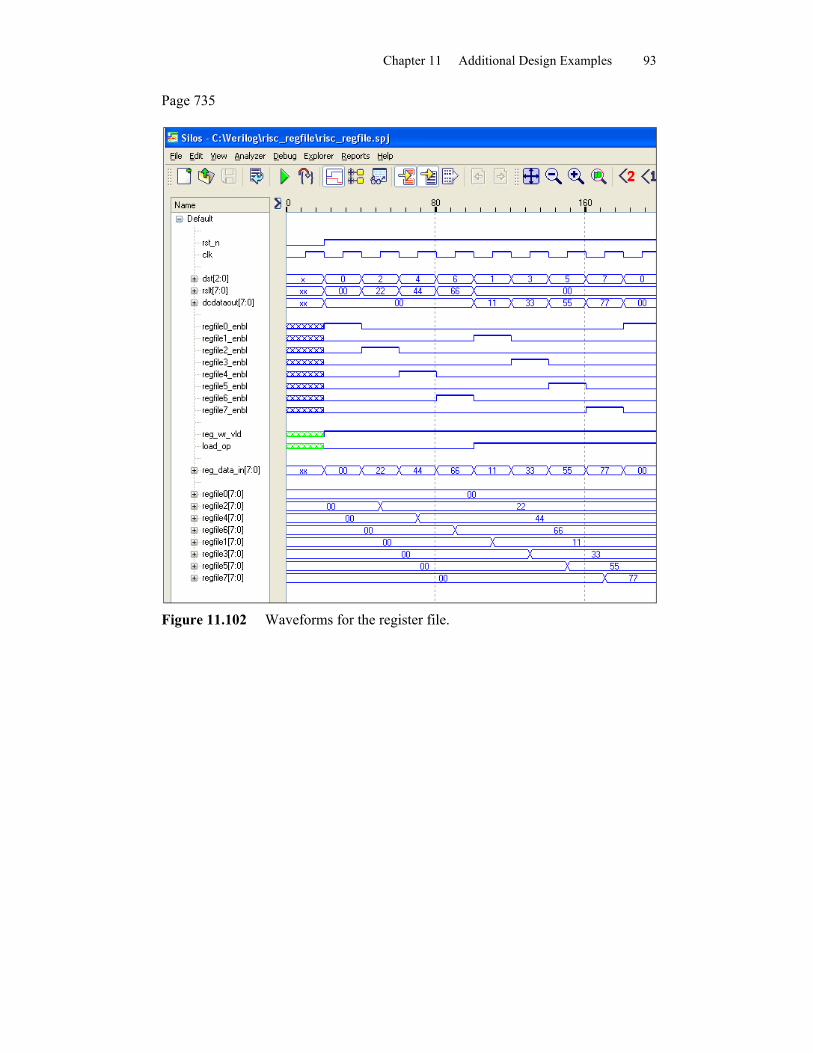
Chapter 11 Additional Design Examples 93
Page 735
Figure 11.102 Waveforms for the register file.

Chapter 11 Additional Design Examples 94
Page 736
//behavioral data cachemodule risc_dcache (dcenbl, dcaddr, dcdatain, dcdataout, rdwr);
input [3:0] dcaddr;input [7:0] dcdatain;input dcenbl, rdwr;output [7:0] dcdataout;
wire [3:0] dcaddr;wire [7:0] dcdatain;wire dcenbl, rdwr;
reg [7:0] dcdataout;
//define memory size: # of bits per reg; # of regs//8 bits per reg; 16 regsreg [7:0] dcache [0:15];
//define memory contentsinitialbegin
dcache [00] = 8'h00;dcache [01] = 8'h22;dcache [02] = 8'h44;dcache [03] = 8'h66;dcache [04] = 8'h88;dcache [05] = 8'haa;dcache [06] = 8'hcc;dcache [07] = 8'hff;dcache [08] = 8'h00;dcache [09] = 8'h00;dcache [10] = 8'h00;dcache [11] = 8'h00;dcache [12] = 8'h00;dcache [13] = 8'h00;dcache [14] = 8'h00;dcache [15] = 8'h00;
end //continued on next page
Figure 11.103 Behavioral module for the data cache.
Chapter 11 Additional Design Examples 95
always @ (dcenbl or dcaddr or dcdatain or rdwr)begin
if (rdwr) //if true, read op (ld regfile)dcdataout = dcache [dcaddr];
else //if false, write op (st regfile)dcache [dcaddr] = dcdatain;
end
endmodule
Figure 11.103 (Continued)
Page 737
//test bench for data cachemodule risc_dcache_tb;
reg [3:0] dcaddr;reg [7:0] dcdatain;reg dcenbl, rdwr;wire [7:0] dcdataout;
//display variablesinitial$monitor ("dcaddr = %b, datain = %h, dataout = %h",
dcaddr, dcdatain, dcdataout);
//read the contents of cacheinitialbegin
#0 dcaddr = 4'b0000; dcdatain = 8'h00;dcenbl = 1'b1; rdwr = 1'b1; //read
#10 dcaddr = 4'b0001; dcenbl = 1'b1; rdwr = 1'b1;#10 dcaddr = 4'b0010; dcenbl = 1'b1; rdwr = 1'b1;#10 dcaddr = 4'b0011; dcenbl = 1'b1; rdwr = 1'b1;#10 dcaddr = 4'b0100; dcenbl = 1'b1; rdwr = 1'b1;#10 dcaddr = 4'b0101; dcenbl = 1'b1; rdwr = 1'b1;#10 dcaddr = 4'b0110; dcenbl = 1'b1; rdwr = 1'b1;#10 dcaddr = 4'b0111; dcenbl = 1'b1; rdwr = 1'b1;
//continued on next page
Figure 11.104 Test bench for the data cache.

Chapter 11 Additional Design Examples 96
//write alternating all 0s and all 1s to cache#10 dcaddr = 4'b1000; dcdatain = 8'h00; dcenbl = 1'b1;
rdwr = 1'b0; //write#10 dcaddr = 4'b1001; dcdatain = 8'hff; dcenbl = 1'b1;
rdwr = 1'b0;#10 dcaddr = 4'b1010; dcdatain = 8'h00; dcenbl = 1'b1;
rdwr = 1'b0;#10 dcaddr = 4'b1011; dcdatain = 8'hff; dcenbl = 1'b1;
rdwr = 1'b0;#10 dcaddr = 4'b1100; dcdatain = 8'h00; dcenbl = 1'b1;
rdwr = 1'b0;#10 dcaddr = 4'b1101; dcdatain = 8'hff; dcenbl = 1'b1;
rdwr = 1'b0;#10 dcaddr = 4'b1110; dcdatain = 8'h00; dcenbl = 1'b1;
rdwr = 1'b0;#10 dcaddr = 4'b1111; dcdatain = 8'hff; dcenbl = 1'b1;
rdwr = 1'b0;
#20 $stop;end
//instantiate the module into the test benchrisc_dcache inst1 (
.dcenbl(dcenbl),
.dcaddr(dcaddr),
.dcdatain(dcdatain),
.dcdataout(dcdataout),
.rdwr(rdwr));
endmodule
Figure 11.104 (Continued)

Chapter 11 Additional Design Examples 97
Page 738
dcaddr = 0000, datain = 00, dataout = 00dcaddr = 0001, datain = 00, dataout = 22dcaddr = 0010, datain = 00, dataout = 44dcaddr = 0011, datain = 00, dataout = 66dcaddr = 0100, datain = 00, dataout = 88dcaddr = 0101, datain = 00, dataout = aadcaddr = 0110, datain = 00, dataout = ccdcaddr = 0111, datain = 00, dataout = ffdcaddr = 1000, datain = 00, dataout = ffdcaddr = 1001, datain = ff, dataout = ffdcaddr = 1010, datain = 00, dataout = ffdcaddr = 1011, datain = ff, dataout = ffdcaddr = 1100, datain = 00, dataout = ffdcaddr = 1101, datain = ff, dataout = ffdcaddr = 1110, datain = 00, dataout = ffdcaddr = 1111, datain = ff, dataout = ff
Figure 11.105 Outputs for the data cache.
Page 739
Figure 11.106 Waveforms for the data cache.

Chapter 11 Additional Design Examples 98
Page 740//structural risc cpu topmodule risc_cpu_top1 (clk, rst_n, instruction, pc, dcenbl,
dcaddr, dcdatain, dcdataout, rdwr);
input clk, rst_n;input [12:0] instruction;output [4:0] pc;output dcenbl, rdwr;output [3:0] dcaddr;output [7:0] dcdatain, dcdataout;
wire [12:0] instruction, instr;wire [4:0] pc;wire [3:0] opcode, dcaddrin;wire [2:0] opnda_addr, opndb_addr, dstin;wire clk, rst_n;wire [2:0] dst;wire [7:0] regfile0_in, regfile1_in, regfile2_in, regfile3_in,
regfile4_in, regfile5_in, regfile6_in, regfile7_in;wire dcenbl, rdwr, reg_wr_vld, load_op;wire [3:0] dcaddr;wire [7:0] result;
risc_iunit inst1 (.instruction(instruction),.pc(pc),.clk(clk),.rst_n(rst_n),.ir(instr));
risc_decode inst2 (.clk(clk),.rst_n(rst_n),.instr(instr),.opcode(opcode),.dcaddr(dcaddrin),.opnda(opnda_addr),.opndb(opndb_addr),.dst(dstin));
risc_eunit inst3 (.clk(clk), //inputs begin here.rst_n(rst_n),.opcode(opcode),
//continued on next page
Figure 11.108 Structural module for the RISC CPU top level.

Chapter 11 Additional Design Examples 99
.dcaddrin(dcaddrin),
.opnda_addr(opnda_addr),
.opndb_addr(opndb_addr),
.dstin(dstin),
.regfile0(regfile0_in),
.regfile1(regfile1_in),
.regfile2(regfile2_in),
.regfile3(regfile3_in),
.regfile4(regfile4_in),
.regfile5(regfile5_in),
.regfile6(regfile6_in),
.regfile7(regfile7_in),
.dcenbl(dcenbl), //outputs begin here
.dcdatain(dcdatain),
.rdwr(rdwr),
.reg_wr_vld(reg_wr_vld),
.dcaddr(dcaddr),
.rslt(result),
.dst(dst),
.load_op(load_op));
risc_regfile inst4 (.clk(clk),.rst_n(rst_n),.reg_wr_vld(reg_wr_vld),.load_op(load_op),.dst(dst),.rslt(result),.dcdataout(dcdataout),.regfile0(regfile0_in),.regfile1(regfile1_in),.regfile2(regfile2_in),.regfile3(regfile3_in),.regfile4(regfile4_in),.regfile5(regfile5_in),.regfile6(regfile6_in),.regfile7(regfile7_in));
endmodule
Figure 11.108 (Continued)

Chapter 11 Additional Design Examples 100
Page 742
//structural system_topmodule risc_system_top (clk, rst_n);
input clk, rst_n;wire clk, rst_n, dcenbl, rdwr;wire [12:0] instruction;wire [4:0] pc;wire [3:0] dcaddr;wire [7:0] dcdatain, dcdataout;
risc_icache inst1 (.pc(pc),.instruction(instruction));
risc_dcache inst2 ( //no clk or rst_n needed.dcenbl(dcenbl),.dcaddr(dcaddr),.dcdatain(dcdatain),.rdwr(rdwr),.dcdataout(dcdataout));
risc_cpu_top1 inst3 (.clk(clk),.rst_n(rst_n),.pc(pc),.instruction(instruction),.dcenbl(dcenbl),.dcaddr(dcaddr),.dcdatain(dcdatain),.rdwr(rdwr),.dcdataout(dcdataout));
endmodule
Figure 11.110 Structural module for the system top pipelined RISC processor.

Chapter 11 Additional Design Examples 101
Page 743
//structural risc_cpu_top test benchmodule risc_system_top_tb;
reg clk, rst_n;
initialbegin
clk = 1'b0;forever
#10 clk = ~clk;end
initialbegin
rst_n = 1'b0;#5 rst_n = 1'b1;#640 $stop; //32 instr times 20 ns per clk cycle
end
risc_system_top inst1 (.clk(clk),.rst_n(rst_n));
endmodule
Figure 11.111 Test bench for the system top module of Figure 11.110.

Chapter 11 Additional Design Examples 102
Page 744
Figure 11.112 Waveforms for the pipelined RISC processor.

Chapter 11 Additional Design Examples 103
Figure 11.112 (Continued)

Chapter 11 Additional Design Examples 104
Figure 11.112 (Continued)