vhdl operator operation - georgia institute of...
TRANSCRIPT

Table 6.1 VHDL Operators.
VHDL Operator Operation + Addition - Subtraction * Multiplication* / Division*
MOD Modulus* REM Remainder*
& Concatenation – used to combine bits SLL** logical shift left SRL** logical shift right SLA** arithmetic shift left SRA** arithmetic shift right ROL** rotate left ROR** rotate right
= equality /= Inequality < less than
<= less that or equal > greater than
>= greater than or equal NOT logical NOT AND logical AND OR logical OR
NAND logical NAND NOR logical NOR XOR logical XOR
XNOR* logical XNOR
*Not supported in many VHDL synthesis tools. In the Quartus II tools, only multiply and divide by powers of two (shifts) are supported. Mod and Rem are not supported in Quartus II. Efficient design of multiply or divide hardware typically requires the user to specify the arithmetic algorithm and design in VHDL. ** Supported only in 1076-1993 VHDL.

Table 6.2 STD_LOGIC conversion functions.
Function Example: CONV_STD_LOGIC_VECTOR( integer, bits ) CONV_STD_LOGIC_VECTOR( 7, 4 )
Converts an integer to a standard logic vector. Useful to enter constants. CONV_SIGNED and CONV_UNSIGNED work in a similar way to produce signed and unsigned values.
Produces a standard logic vector of "0111".
CONV_INTEGER( std_logic_vector ) CONV_INTEGER( "0111" ) Converts a standard logic vector to an integer. Useful for array indexing when using a std_logic_vector signal for the array index.
Produces an integer value of 7.

A
BC
D(1)D(2)
Y
A
BC
D(1)D(2)
X

LIBRARY IEEE; -- Include Libraries for standard logic data typesUSE IEEE.STD_LOGIC_1164.ALL;
-- Entity name normally the same as file nameENTITY gate_network IS -- Ports: Declares module inputs and outputs
PORT( A, B, C : IN STD_LOGIC;-- Standard Logic Vector ( Array of 4 Bits )
D : IN STD_LOGIC_VECTOR( 3 DOWNTO 0 );-- Output Signals
X, Y : OUT STD_LOGIC );END gate_network;
-- Defines internal module architectureARCHITECTURE behavior OF gate_network ISBEGIN -- Concurrent assignment statements operate in parallel
-- D(1) selects bit 1 of standard logic vector DX <= A AND NOT( B OR C ) AND ( D( 1 ) XOR D( 2 ) );
-- Process must declare a sensitivity list, -- In this case it is ( A, B, C, D )-- List includes all signals that can change the outputs
PROCESS ( A, B, C, D )BEGIN -- Statements inside process execute sequentially
Y <= A AND NOT( B OR C) AND ( D( 1) XOR D( 2 ) );END PROCESS;
END behavior;

LED_MSD_DISPLAY: -- BCD to 7 Segment Decoder for LED Displays PROCESS (MSD) BEGIN -- Case statement implements a logic truth table CASE MSD IS WHEN "0000" => MSD_7SEG <= "1111110"; WHEN "0001" => MSD_7SEG <= "0110000"; WHEN "0010" => MSD_7SEG <= "1101101"; WHEN "0011" => MSD_7SEG <= "1111001"; WHEN "0100" => MSD_7SEG <= "0110011"; WHEN "0101" => MSD_7SEG <= "1011011"; WHEN "0110" => MSD_7SEG <= "1011111"; WHEN "0111" => MSD_7SEG <= "1110000"; WHEN "1000" => MSD_7SEG <= "1111111"; WHEN "1001" => MSD_7SEG <= "1111011"; WHEN OTHERS => MSD_7SEG <= "0111110"; END CASE; END PROCESS LED_MSD_DISPLAY;
a
b
c
d
e
fg
dp

LIBRARY IEEE; USE IEEE.STD_LOGIC_1164.ALL; ENTITY multiplexer IS -- Input Signals and Mux Control PORT( A, B, Mux_Control : IN STD_LOGIC; Mux_Out1, Mux_Out2, Mux_Out3, Mux_Out4 : OUT STD_LOGIC ); END multiplexer; ARCHITECTURE behavior OF multiplexer IS BEGIN -- selected signal assignment statement… Mux_Out1 <= A WHEN Mux_Control = '0' ELSE B; -- … with Select Statement WITH mux_control SELECT Mux_Out2 <= A WHEN '0', B WHEN '1', A WHEN OTHERS; -- OTHERS case required since STD_LOGIC -- has values other than "0" or "1" PROCESS ( A, B, Mux_Contro l) BEGIN -- Statements inside a process IF Mux_Control = '0' THEN -- execute sequentially. Mux_Out3 <= A; ELSE Mux_out3 <= B; END IF; CASE Mux_Control IS WHEN '0' => Mux_Out4 <= A; WHEN '1' => Mux_Out4 <= B; WHEN OTHERS => Mux_Out4 <= A; END CASE; END PROCESS; END behavior;
0
1
Mux_Control
Mux_Outx
A
B

LIBRARY IEEE;USE IEEE.STD_LOGIC_1164.ALL;
ENTITY tristate ISPORT( A, Control : IN STD_LOGIC;
Tri_out : INOUT STD_LOGIC); -- Use Inout for bi-directional tri-state-- signals or out for output only
END tristate;
ARCHITECTURE behavior OF tristate IS -- defines internal module architectureBEGIN
Tri_out <= A WHEN Control = '0' ELSE 'Z'; -- Assignment of 'Z' value generates END behavior; -- tri-state output
Control
Tri_OutA

LIBRARY IEEE; USE IEEE.STD_LOGIC_1164.ALL; ENTITY DFFs IS PORT( D, Clock, Reset, Enable : IN STD_LOGIC; Q1, Q2, Q3, Q4 : OUT STD_LOGIC ); END DFFs; ARCHITECTURE behavior OF DFFs IS BEGIN PROCESS -- Positive edge triggered D flip-flop BEGIN -- If WAIT is used no sensitivity list is used WAIT UNTIL ( Clock 'EVENT AND Clock = '1' ); Q1 <= D; END PROCESS;
Q1D D Q
Clock

PROCESS -- Positive edge triggered D flip-flop BEGIN -- with synchronous reset WAIT UNTIL ( Clock 'EVENT AND Clock = '1' ); IF reset = '1' THEN Q2 <= '0'; ELSE Q2 <= D; END IF; END PROCESS; PROCESS (Reset,Clock) -- Positive edge triggered D flip-flop BEGIN -- with asynchronous reset IF reset = '1' THEN Q3 <= '0'; ELSIF ( clock 'EVENT AND clock = '1' ) THEN Q3 <= D; END IF; END PROCESS; PROCESS (Reset,Clock) -- Positive edge triggered D flip-flop BEGIN -- with asynchronous reset and -- enable IF reset = '1' THEN Q4 <= '0'; ELSIF ( clock 'EVENT AND clock = '1' ) THEN IF Enable = '1' THEN Q4 <= D; END IF; END IF; END PROCESS; END behavior;
Q20
1
Reset
D
0
Q3
D Q Q40
1
Enable
Q4
D
Clock
D
Reset
D Q
Clock
Reset
D Q
Clock

LIBRARY IEEE; USE IEEE.STD_LOGIC_1164.ALL; ENTITY ilatch IS PORT( A, B : IN STD_LOGIC; Output1, Output2 : OUT STD_LOGIC ); END ilatch; ARCHITECTURE behavior OF ilatch IS BEGIN PROCESS ( A, B ) BEGIN IF A = '0' THEN Output1 <= '0'; Output2 <= '0'; ELSE IF B = '1' THEN Output1 <= '1'; Output2 <= '1'; ELSE -- Latch inferred since no value is assigned Output1 <= '0'; -- to output2 in the else clause! END IF; END IF; END PROCESS; END behavior;
Output2D Q
Clock

LIBRARY IEEE; USE IEEE.STD_LOGIC_1164.ALL; USE IEEE.STD_LOGIC_ARITH.ALL; USE IEEE.STD_LOGIC_UNSIGNED.ALL; ENTITY Counter IS PORT( Clock, Reset : IN STD_LOGIC; Max_count : IN STD_LOGIC_VECTOR( 7 DOWNTO 0 ); Count : OUT STD_LOGIC_VECTOR( 7 DOWNTO 0 ) ); END Counter; ARCHITECTURE behavior OF Counter IS -- Declare signal(s) internal to module SIGNAL internal_count : STD_LOGIC_VECTOR( 7 DOWNTO 0 ); BEGIN count <= internal_count; PROCESS ( Reset,Clock ) BEGIN -- Reset counter IF reset = '1' THEN internal_count <= "00000000"; ELSIF ( clock 'EVENT AND clock = '1' ) THEN IF internal_count < Max_count THEN -- Check for maximum count internal_count <= internal_count + 1; -- Increment Counter ELSE -- Count >= Max_Count internal_count <= "00000000"; -- reset Counter END IF; END IF; END PROCESS; END behavior;

A
Re s e t
CBOutput 1
X1
1 X 0X
X0
Figure 6.1 State Diagram for st_mach example

LIBRARY IEEE; USE IEEE.STD_LOGIC_1164.ALL; ENTITY st_mach IS PORT( clk, reset : IN STD_LOGIC; Input1, Input2 : IN STD_LOGIC; Output1 : OUT STD_LOGIC); END st_mach; ARCHITECTURE A OF st_mach IS -- Enumerated Data Type for State TYPE STATE_TYPE IS ( state_A, state_B, state_C ); SIGNAL state: STATE_TYPE; BEGIN PROCESS ( reset, clk ) BEGIN IF reset = '1' THEN -- Reset State state <= state_A; ELSIF clk 'EVENT AND clk = '1' THEN

CASE state IS -- Define Next State Transitions using a Case -- Statement based on the Current State WHEN state_A => IF Input1 = '0' THEN state <= state_B; ELSE state <= state_C; END IF; WHEN state_B => state <= state_C; WHEN state_C => IF Input2 = '1' THEN state <= state_A; END IF; WHEN OTHERS => state <= state_A; END CASE; END IF; END PROCESS; WITH state SELECT -- Define State Machine Outputs Output1 <= '0' WHEN state_A, '1' WHEN state_B, '0' WHEN state_C; END a;

LIBRARY IEEE; USE IEEE.STD_LOGIC_1164.ALL; USE IEEE.STD_LOGIC_ARITH.ALL; USE IEEE.STD_LOGIC_UNSIGNED.ALL; ENTITY ALU IS PORT( Op_code : IN STD_LOGIC_VECTOR( 2 DOWNTO 0 ); A_input, B_input : IN STD_LOGIC_VECTOR( 7 DOWNTO 0 ); ALU_output : OUT STD_LOGIC_VECTOR( 7 DOWNTO 0 ) ); END ALU; ARCHITECTURE behavior OF ALU IS -- Declare signal(s) internal to module here SIGNAL temp_output : STD_LOGIC_VECTOR( 7 DOWNTO 0 ); BEGIN PROCESS ( Op_code, A_input, B_input ) BEGIN

CASE Op_Code ( 2 DOWNTO 1 ) IS -- Select Arithmetic/Logical Operation WHEN "00" => temp_output <= A_input + B_input; WHEN "01" => temp_output <= A_input - B_input; WHEN "10" => temp_output <= A_input AND B_input; WHEN "11" => temp_output <= A_input OR B_input; WHEN OTHERS => temp_output <= "00000000"; END CASE; -- Select Shift Operation: Shift bits left with zero fill using concatenation operator -- Can also use VHDL 1076-1993 shift operator such as SLL IF Op_Code( 0 ) = '1' THEN Alu_output <= temp_output( 6 DOWNTO 0 ) & '0'; ELSE Alu_output <= temp_output; END IF; END PROCESS; END behavior;
A_input B_input
8
8
Op_code(2 downto 1)
ALU+, -, AND, OR
Temp_output
Shif t
ALU_output
8
Op_code (0)

LIBRARY IEEE; USE IEEE.STD_LOGIC_1164.ALL; USE IEEE.STD_LOGIC_ARITH.ALL; USE IEEE.STD_LOGIC_UNSIGNED.ALL; LIBRARY lpm; USE lpm.lpm_components.ALL; ENTITY mult IS PORT( A, B : IN STD_LOGIC_VECTOR( 7 DOWNTO 0 ); Product : OUT STD_LOGIC_VECTOR( 15 DOWNTO 0 ) ); END mult; ARCHITECTURE a OF mult IS BEGIN -- LPM 8x8 multiply function P = A * B multiply: lpm_mult GENERIC MAP( LPM_WIDTHA => 8, LPM_WIDTHB => 8, LPM_WIDTHS => 16, LPM_WIDTHP => 16, LPM_REPRESENTATION => "UNSIGNED" ) PORT MAP ( data => A, datab => B, result => Product ); END a;

LIBRARY IEEE; USE IEEE.STD_LOGIC_1164.ALL; ENTITY memory IS PORT( read_data : OUT STD_LOGIC_VECTOR( 7 DOWNTO 0 ); read_address : IN STD_LOGIC_VECTOR( 2 DOWNTO 0 ); write_data : IN STD_LOGIC_VECTOR( 7 DOWNTO 0 ); write_address : IN STD_LOGIC_VECTOR( 2 DOWNTO 0 ); Memwrite : IN STD_LOGIC; Clock : IN STD_LOGIC ); END memory; ARCHITECTURE behavior OF memory IS -- define new data type for memory array TYPE memory_type IS ARRAY ( 0 TO 7 ) OF STD_LOGIC_VECTOR( 7 DOWNTO 0 ); SIGNAL memory : memory_type; BEGIN -- Read Memory and convert array index to an integer with CONV_INTEGER read_data <= memory( CONV_INTEGER( read_address( 2 DOWNTO 0 ) ) ); PROCESS -- Write Memory? BEGIN WAIT UNTIL clock 'EVENT AND clock = '1'; IF ( memwrite = '1' ) THEN -- convert array index to an integer with CONV_INTEGER memory( CONV_INTEGER( write_address( 2 DOWNTO 0 ) ) ) <= write_data; END IF; END PROCESS; END behavior;

LIBRARY IEEE; USE IEEE.STD_LOGIC_1164.ALL; ENTITY memory IS PORT( read_data : OUT STD_LOGIC_VECTOR( 7 DOWNTO 0 ); read_address : IN STD_LOGIC_VECTOR( 2 DOWNTO 0 ); write_data : IN STD_LOGIC_VECTOR( 7 DOWNTO 0 ); write_address : IN STD_LOGIC_VECTOR( 2 DOWNTO 0 ); Memwrite : IN STD_LOGIC; clock,reset : IN STD_LOGIC ); END memory; ARCHITECTURE behavior OF memory IS SIGNAL mem0, mem1 : STD_LOGIC_VECTOR( 7 DOWNTO 0 ); BEGIN PROCESS (read_address, mem0, mem1) -- Process for memory read operation BEGIN CASE read_address IS WHEN "000" => read_data <= mem0; WHEN "001" => read_data <= mem1; WHEN OTHERS => -- Unimplemented memory locations read_data <= X"FF"; END CASE; END PROCESS;

PROCESS BEGIN WAIT UNTIL clock 'EVENT AND clock = '1'; IF ( reset = '1' ) THEN mem0 <= X"55" ; -- Initial values for memory (optional) mem1 <= X"AA" ; ELSE IF memwrite = '1' THEN -- Write to memory? CASE write_address IS -- Use a flip-flop with WHEN "000" => -- an enable for memory mem0 <= write_data; WHEN "001" => mem1 <= write_data; WHEN OTHERS => -- unimplemented memory locations NULL; END CASE; END IF; END IF; END PROCESS; END behavior;
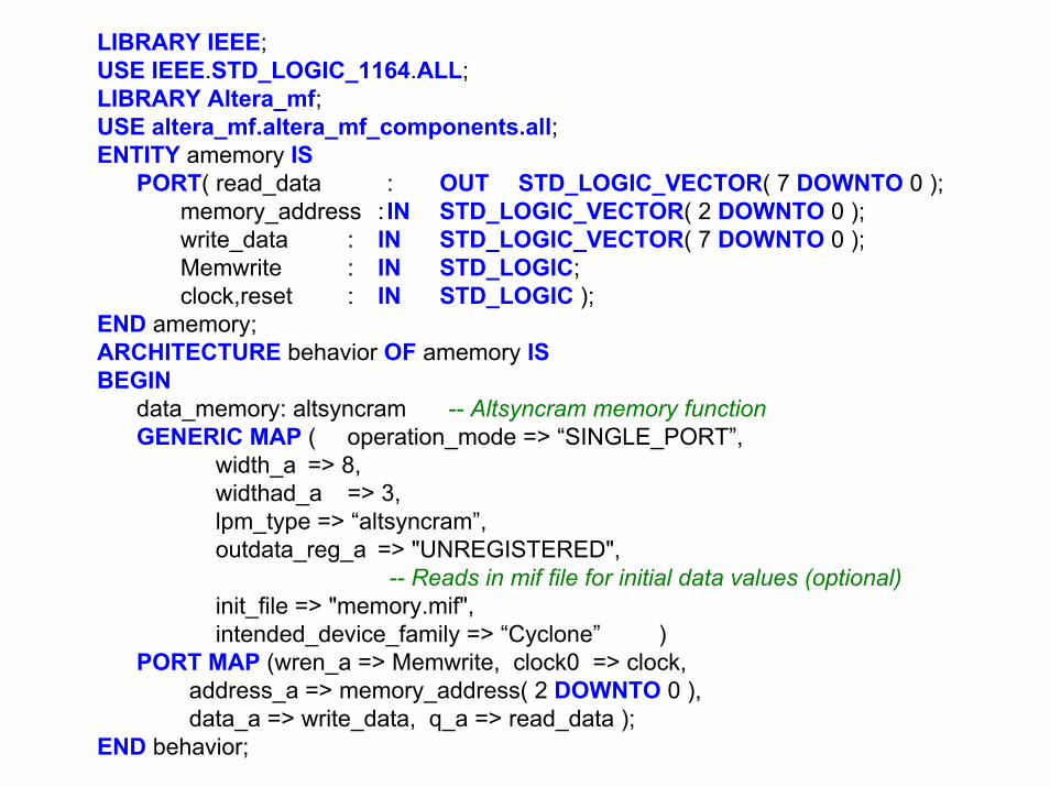
LIBRARY IEEE;USE IEEE.STD_LOGIC_1164.ALL;LIBRARY Altera_mf;USE altera_mf.altera_mf_components.all;ENTITY amemory IS
PORT( read_data : OUT STD_LOGIC_VECTOR( 7 DOWNTO 0 );memory_address : IN STD_LOGIC_VECTOR( 2 DOWNTO 0 );write_data : IN STD_LOGIC_VECTOR( 7 DOWNTO 0 );Memwrite : IN STD_LOGIC;clock,reset : IN STD_LOGIC );
END amemory;ARCHITECTURE behavior OF amemory ISBEGIN
data_memory: altsyncram -- Altsyncram memory functionGENERIC MAP ( operation_mode => “SINGLE_PORT”,
width_a => 8,widthad_a => 3,lpm_type => “altsyncram”,outdata_reg_a => "UNREGISTERED",
-- Reads in mif file for initial data values (optional)init_file => "memory.mif",intended_device_family => “Cyclone” )
PORT MAP (wren_a => Memwrite, clock0 => clock, address_a => memory_address( 2 DOWNTO 0 ), data_a => write_data, q_a => read_data );
END behavior;

clock_48Mhz clock_1MHz
clock_100KHz
clock_10KHz
clock_1KHz
clock_100Hz
clock_10Hz
clock_1Hz
clk_div
inst
pb
clock_100Hz
pb_debounced
debounce
inst1
PB_debounced
clock
PB_single_pulse
onepulse
inst2
PB1_Single_PulsePB1_DebouncedPB1
Clock_48Mhz
Clock_100Hz
Clock_1Mhz
Figure 6.2 Schematic of Hierarchical Design

ENTITY hierarch ISPORT ( clock_25Mhz, pb1 : IN STD_LOGIC;
pb1_single_pulse : OUT STD_LOGIC);END hierarch;ARCHITECTURE structural OF hierarch IS -- Declare internal signals needed to connect submodulesSIGNAL clock_1MHz, clock_100Hz, pb1_debounced : STD_LOGIC;
COMPONENT debounce -- Use Components to Define Submodules and Parameters
PORT( pb, clock_100Hz : IN STD_LOGIC;pb_debounced : OUT STD_LOGIC);
END COMPONENT;COMPONENT onepulse
PORT(pb_debounced, clock : IN STD_LOGIC;pb_single_pulse : OUT STD_LOGIC);
END COMPONENT;COMPONENT clk_div
PORT( clock_25Mhz : IN STD_LOGIC;clock_1MHz : OUT STD_LOGIC;clock_100KHz : OUT STD_LOGIC;clock_10KHz : OUT STD_LOGIC;clock_1KHz : OUT STD_LOGIC;clock_100Hz : OUT STD_LOGIC;clock_10Hz : OUT STD_LOGIC;clock_1Hz : OUT STD_LOGIC);
END COMPONENT;BEGIN -- Use Port Map to connect signals between components in the hierarchydebounce1 : debounce PORT MAP ( pb => pb1, clock_100Hz = >clock_100Hz,
pb_debounced = >pb1_debounced);prescalar : clk_div PORT MAP ( clock_25Mhz = >clock_25Mhz,
clock_1MHz =>clock_1Mhz, clock_100hz = >clock_100hz);
single_pulse : onepulse PORT MAP ( pb_debounced = >pb1_debounced, clock => clock_1MHz, pb_single_pulse => pb1_single_pulse);
END structural;

Hardware UUT
Response Monitor
Stimulus Generator
Testbench
Figure 6.3 Using a Testbench for automatic verification