video and image processing design example - altera · pdf filevideo and image processing...
TRANSCRIPT

February 2013 Altera Corporation
AN-427-10.2
© 2013 Altera Corporation. AlQUARTUS and STRATIX worOffice and in other countries. respective holders as describedproducts to current specificatioproducts and services at any tiof any information, product, oadvised to obtain the latest verfor products or services.
101 Innovation DriveSan Jose, CA 95134www.altera.com
Video and Image Processing DesignExample
Application Note
The Altera® Video and Image Processing Design Example demonstrates the following items:
■ A framework for rapid development of video and image processing systems
■ Dynamic scaling, clipping, flashing, moving, sharpening and FIR filtering of both standard definition (SD) and high definition (HD) inputs
■ Picture-in-picture mixing with a background layer
■ Run-time control of different parts of the system, including a radar that uses on-screen display functions.
■ Debugging components for monitoring the video stream from within the datapath
The design example runs from the Bitec HSMC DVI and Bitec HSMC Quad Video daughtercards. The standard definition video stream is in either National Television System Committee (NTSC) or phase alternation line (PAL) format. The high-definition video stream uses a digital video interface (DVI) port.
The design example uses some of the parameterizable IP cores that are available in the Video and Image Processing Suite. Table 1 shows some of the available IP cores.
Table 1. Video and Image Processing Suite IP Cores
IP Core Description
2D FIR Filter Performs 2D convolution using matrices of 3×3, 5×5, or 7×7 coefficients.
2D Median Filter Applies 3×3, 5×5, or 7×7 pixel median filters to video images.
Alpha Blending Mixer Mixes up to 12 input image layers.
Avalon-ST Video Monitor Captures video data packets without adding additional delays and connects to trace system IP cores for collecting video trace data.
Chroma Resampler Resamples video data to and from common sampling formats.
Clipper Clips video streams.
Clocked Video Input Converts clocked video formats to Avalon® Streaming (Avalon-ST) Video.
Clocked Video Output Converts Avalon-ST Video to clocked video formats.
Color Plane Sequencer Changes how color plane samples transmit across an Avalon-ST interface.
Color Space Converter Transforms video data between color spaces.
Control Synchronizer Synchronizes video stream changes with control port changes.
Deinterlacer II Converts interlaced video to progressive video.
Frame Buffer Buffers video frames into external RAM.
Frame Reader Reads a video frame from external RAM.
Gamma Corrector Corrects video streams for the physical properties of display devices.
Interlacer Converts progressive video to interlaced video.
l rights reserved. ALTERA, ARRIA, CYCLONE, HARDCOPY, MAX, MEGACORE, NIOS, ds and logos are trademarks of Altera Corporation and registered in the U.S. Patent and Trademark All other words and logos identified as trademarks or service marks are the property of their
at www.altera.com/common/legal.html. Altera warrants performance of its semiconductor ns in accordance with Altera's standard warranty, but reserves the right to make changes to any
me without notice. Altera assumes no responsibility or liability arising out of the application or use r service described herein except as expressly agreed to in writing by Altera. Altera customers are sion of device specifications before relying on any published information and before placing orders
Feedback Subscribe
ISO 9001:2008 Registered

Page 2
f For more information about these IP cores, refer to the Video and Image Processing Suite User Guide.
These IP cores allow you to fully integrate common video functions with video interfaces, processors, and external memory controllers.
The design example targets an Altera Cyclone® III EP3C120 development board connected by high-speed mezzanine card (HSMC) interfaces to Bitec HSMC Quad Video and DVI daughtercards. the bitec daughtercards are available with the Cyclone III Video Processing Development Kit.
f For more information on the Cyclone III Video Processing Development Kit, refer to the Bitec website.
f For information about the EP3C120 development board, refer to the Cyclone III Development Board Reference Manual.
The design example accepts either composite or DVI video sources. The composite input is through an analog composite port on a Bitec HSMC Quad Video daughtercard, which generates a digital output in BT656 format. The DVI input is through the RX port on a Bitec HSMC DVI daughtercard.
The design example performs the following common video functions on the two input streams in the FPGA:
■ Clipping
■ Chroma resampling
■ Motion adaptive deinterlacing
■ Color space conversion
■ Picture-in-picture mixing
■ Gamma correction
■ FIR filtering
■ Polyphase scaling
The design example uses software on a Nios® II processor to configure and initialize to input and output video interfaces on the two HSMC daughtercards (TVP5154 and TFP410 chips). The Nios II software demonstrates how to control the clocked video input, clocked video output, and mixer functions at run-time.
Scaler II Resizes video streams.
Test Pattern Generator Generates a test pattern video stream.
Trace System Monitors captured data from video monitor and connects to host System Console via JTAG or USB for display.
Switch Switches video streams on frame boundaries at run time.
Table 1. Video and Image Processing Suite IP Cores
IP Core Description
Video and Image Processing Design Example February 2013 Altera Corporation

New in Version 10.0 Page 3
The design example uses the Qsys system-level design tool to implement the video system. Qsys provides an easy path to system integration of the video processing datapath. Qsys is a system development tool that allows you to create hardware and software system modules with a customized set of system peripherals. Qsys automatically creates the bus arbitration logic connecting the individual components together to create an overall system.
f For more information about Qsys, refer to the System Design with Qsys section in volume 1 of the Quartus II Handbook.
The Video and Image Processing Suite IP cores have common open Avalon-ST data interfaces and Avalon Memory-Mapped (Avalon-MM) control interfaces to ease connection of a chain of video functions and video system modeling. In addition, the IP cores use the Avalon-ST Video protocol to transmit video data between them, to help you build run-time controllable systems and for easy error recovery.
f For a full description of how the Avalon-ST Video protocol and Avalon interfaces are implemented, refer to the Interfaces chapter in the Video and Image Processing Suite User Guide.
f For more information about the Avalon-MM and Avalon-ST interfaces, refer to the Avalon Interface Specifications.
New in Version 10.0
DisplayThe design v10.0 includes a DVI input, and uses the Nios II processor to create a graphical overlay display of a radar. The design examines the composite and DVI inputs and ignores inputs that are not currently connected to the system. The design outputs text on the screen, to describe each step it demonstrates. The design shows a radar with moving enemies and a frames per second (FPS) indicator.
New IP CoresThe design v10.0 includes the following IP cores:
■ The Scaler II IP core, which includes new functionality, specifically adding edge adaptive and nearest neighbor scaling algorithms.
■ The Deinterlacer II IP core, which includes cadence detection algorithms: 2:2 detector and 3:2 and 2:2 detector.
DebuggingThe design v10.0 includes a debugging system. This system taps all the signals between some IP cores, and send this data to a host machine running System Console. System Console then provides high-level meaningful visualizations of this data, which allows you to easily debug your design.
Video and Image Processing Design ExampleFebruary 2013 Altera Corporation

Page 4 Design Example Overview
Design Example OverviewThe design example shows on a suitable screen a range of functions, including scaling, clipping, flashing, moving and sharpening on the composite input. If a DVI input source is present the design then shows it, clipping, scaling, moving and applying filters to it. Finally the two video streams move to the corners of the screen and the design uses Nios II functions to demonstrate the radar view, which shows a sweeping scanner line and tracking enemies moving across the screen. (Figure 1).
The Video and Image Processing Design Example demonstrates a simple, yet highly parameterizable, design flow for rapid system development.
The design uses the following software:
■ Qsys for abstract design capture, parameterizable IP cores, and switch fabric generation
■ The Quartus II software for pin mapping and to interface IP cores
■ The Nios II Software Build Tools for Eclipse for run-time software control and configuration
■ Quartus II SignalTap and Qsys System Console for debugging
The design provides the following features:
■ Open interface and protocol standards to enable design reuse and connection of custom IP cores with off-the-shelf IP including:
■ Data streaming interfaces and protocols for transmission of video data between IP cores in the system (Avalon-ST Video protocol layers on the Avalon-ST interface).
■ Control interfaces (Avalon-MM master and slave interfaces).
■ Random access to external memory (Avalon-MM master and slave interfaces).
Figure 1. Video Stream Output
[FPS:60]DEMO END, THANK YOUFOR WATCHING
Video and Image Processing Design Example February 2013 Altera Corporation

Design Example Overview Page 5
■ System-level tools and design methodology for rapid system construction, integration, and redesign. The Qsys tool uses standard interfaces to present an abstract view of the design and generates an application-specific switch fabric to construct the system.
■ Parameterizable IP cores that enable you to quickly construct complete video systems.
■ System debugging functionality allows you to tap and view signals in the datapath. You can decode them into accessible visual representations in real time, allowing for rapid debugging while creating designs.
■ Reference designs that demonstrate the capabilities of the video and image processing IP cores.
■ Development kits to rapidly prototype the designs.
QsysThe Qsys flow is the primary design flow for rapid video system development. Specifically, Qsys simplifies the process of system design, including the datapath, processor core, and external memory integration. Qsys enables you to capture the design at an abstract level, with single point-to-point data connections rather than connecting individual data and control interface wires.
All connections in the Qsys system use Avalon-ST and Avalon-MM interfaces. You can connect Video and Image Processing Suite IP cores that support Avalon-ST Video protocol for data transmission with the click of a button.
Qsys automatically generates an interconnect switch fabric, including arbitration logic to connect the memory mapped masters and slaves together. A common example is a system that uses a single memory controller but contains multiple Avalon-MM masters that buffer video data in an external memory.
Figure 2 shows the Qsys system main external connections.
Video Input from an External Video InterfaceThe design uses parameterizable Clocked Video Input IP cores to connect to the external video interface. This IP core provides a bridge between a clocked video interface, such as a serial digital interface (SDI) IP core, and the Avalon-ST Video flow controlled domain.
Figure 2. External Connections to Qsys System
Composite input from Bitec Quad
Video cardDVI Tx output on BitecDVI Video card
External MemoryInterface
Qsys SystemDVI input
from Bitec QuadVideo card
Video and Image Processing Design ExampleFebruary 2013 Altera Corporation

Page 6 Design Example Overview
Video Output to an External Video InterfaceThe design uses a parameterizable Clocked Video Output IP core to connect to the external video interface. This IP core provides a bridge between the Avalon-ST Video flow controlled domain and a clocked video interface (such as DVI).
Connection to an External Memory InterfaceThe design uses an Altera DDR2 SDRAM Controller IP core to connect to the external memory interface. Qsys generates the application-specific switch fabric to arbitrate between multiple masters trying to access the controller.
f For information about Qsys, refer to Creating a System with Qsys chapter in volume 1 of the Quartus II Handbook.
Quartus II SoftwareThe Quartus II software environment describes the top-level system and integrates the Qsys system into the top-level design.
The Quartus II software environment maps the Qsys system external connections as exported wires to video interface IP cores (such as SDI) and memory interfaces (such as DDR2). It also makes the appropriate pin assignments. The Quartus II software includes a wide range of tools to help with timing closure and perform hardware compilation to generate an FPGA programming file.
In addition, the Quartus II software provides the SignalTap™ II Logic Analyzer, a system-level debugging tool that captures and displays real-time signal behavior allowing you to observe interactions between hardware and software in system designs.
f For information about the Quartus II software, refer to the Quartus II Help.
Nios II Software Build Tools for EclipseThe Nios II Software Build Tools (SBT) for Eclipse is the primary software development tool for the Nios II family of embedded processors. You can perform all software development tasks within the Nios II SBT for Eclipse, including editing, building, and debugging programs. The Nios II SBT for Eclipse provides a consistent development platform that supports all Nios II processor systems.
You can configure video interfaces and control video processing functions in the Nios II SBT for Eclipse software. These features provide a very rapid development cycle for software control code changes, without requiring hardware recompilation. This environment provides you with all the standard software debug tools, including breakpoints, views of memory, variables, and registers, and single stepping.
C++ software classes provide a software application programming interface (API) between the Nios II control code and the Video and Image Processing Suite IP cores. The C++ classes contain member functions to provide easy control of the IP cores and easy access to useful data flow information such as the number of frames that the design drops or repeats by a frame buffer in the datapath.
Video and Image Processing Design Example February 2013 Altera Corporation
Design Example Overview Page 7
f For information about the Nios II SBT for Eclipse software, refer to the Nios II Software Developer’s Handbook.
System ConsoleSystem Console is the Altera flexible system-level debugging tool that helps you quickly and efficiently debug your design while the design is running at full speed in an FPGA. System Console enables you to send read and write system-level transactions into your Qsys system to help isolate and identify problems. It also provides a quick and easy way to check system clocks and monitor reset states, which can be particularly helpful during board bring-up. In addition, System Console allows you use graphical elements, such as buttons, dials, and graphs, to create your own custom verification or demonstration to represent many system-level transactions and monitor the processing of data.
If you connect System Console to a design that contains a Trace System IP core, such as this design example, the Trace Table View option appears under the Tools menu. This option allows you to view the contents of the monitors connected to the trace system.
The trace system allows you to view high-level information about the signals passing between video and image processing IP cores, allowing for rapid debugging of problems. You can tap and capture video data passing through by placing monitors into the system. System Console encapsulates and transfers the captured data through either a JTAG or a USB interface to an attached host machine.
f For more information about System Console, refer to the Analyzing and Debugging Designs with the System Console chapter in volume 3 of the Quartus II Handbook.
System Console receives this data and displays it in a real-time table view, with high-level decoding of each packet's contents. The table view allows you to filter and search the data stream. You can also communicate with the monitors in the system to further configure them.
Video and Image Processing Design ExampleFebruary 2013 Altera Corporation

Page 8 Functional Description
Functional DescriptionFigure 3 on page 8 shows a block diagram for the Video and Image Processing Design Example.
The design comprises the following blocks:
■ Composite and DVI video path
■ A Nios II processor for run time control
■ DDR2 SDRAM controller for external and on-chip memory
■ A five layer Alpha Blend Mixer with the following layers:
■ The composite and DVI video input paths.
■ Scan layer, which contains dynamic objects in the radar. This layer is double buffered. The design switches the frame every time it finishes a render and it transfers one complete frame.
■ Graphic overlay, for the static foreground of the radar and also displays information in the demonstration.
■ Background layer, to give a solid black color.
The design also includes the following components that are not on the block diagram:
■ Interval timer
■ Vectored interrupt controller
■ I2C bus masters
■ Debugging system
Figure 3. Design Example Block Diagram
ClockedVideoOutput
BackgroundLayer
CompositeVideo
Input Path
Nios IIProcessor
DDR2SDRAM Controller
Compositeinput from
Bitec QuadVideo Board
DVIVideo
Input Path
Graphic Overlay (Radar)
Avalon-STVideo
Monitor 1
ScanLayer
DVIinput from
Bitec QuadVideo Board
DVI Txfrom BitecDVI Video
Qsys System
AlphaBlending
Mixer
Video and Image Processing Design Example February 2013 Altera Corporation

Functional Description Page 9
All layers require access to the DDR2 SDRAM. Because of the bandwidth limitation, the design limits the DVI video to a maximum resolution of 960x540 after the first clipper. For higher bandwidth requirements, you can use the top bank of the DDR2 SDRAM.
All Video and Image Processing Suite IP cores (except the Line Buffer Compiler) use the Avalon-ST Video protocol to transmit data, which increases productivity through design flexibility and reuse.
f For more information about the Avalon-ST Video protocol, refer to the Video and Image Processing Suite User Guide.
Video Input PathsThe design example has the following video processing datapaths:
■ Composite (NTSC and PAL)
■ DVI (720p60, 720p50, 720p25, 720p24, 1080p25 or 1080p24 video stream)
You may input a composite video stream (BT656 format) via the first composite input port (Figure 3) on the Bitec Quad Video daughtercard or for DVI input via the RX DVI port. The TVP5154 video decoder chip on the Bitec Quad Video daughtercard performs analog-to-digital conversion of the video input signals, which you must configure using the I2C interface.
The Nios II processor controls the configuration of the decoder chip by writing and reading data to and from the I2C bus controller, which performs writes and reads on the external bus as requested.
The video stream, with active picture data in YCbCr 4:2:2 or RGB format and associated embedded synchronization signals, is input from a daughtercard into the Clocked Video Input IP core on the FPGA. This IP core converts from a notionally clocked video format (such as BT656 or DVI) to the flow controlled Avalon-ST Video protocol. The clocked video input forms the boundary of the Qsys design at the input. the design exports the clocked video signals to the top-level system for connection to the input pins from the Quad Video daughtercard.
The Clocked Video Input IP core strips the incoming clocked video of horizontal and vertical blanking, leaving active picture data. The Clocked Video Input IP core uses this data with horizontal and vertical synchronization information, to create the necessary Avalon-ST Video control and active picture packets.
The design does not convert the active picture data; the color plane information remains the same as in the clocked video format.
The clocked video input also provides clock crossing capabilities to allow video formats running at different frequencies to enter the system. The clocked video input also provides greater design flexibility and enables the design to decouple the video processing system clock from the video input pixel clock. In this example, the pixel clock is 27 MHz and the system clock is 100 MHz.
In addition to configuring the TVP5154 decoder chip, the Nios II processor starts all the clocked video inputs in the system.
Video and Image Processing Design ExampleFebruary 2013 Altera Corporation

Page 10 Functional Description
CompositeThe video processing datapath is a chain of parameterizable video processing, integration, and buffering functions from the Video and Image Processing Suite. Figure 4 shows a block diagram of the composite datapath.
The vip_top.v file shows the exported signals in system instantiation (Figure 5).
NTSC Video Stream Input
The NTSC video stream input into the datapath is 8 bits wide, in YCbCr 4:2:2 interlaced format, with each field input containing 720 pixels per line, and either 244 lines for each even field (f0) and 243 lines for each odd field (f1). The design transmits the luma (Y) and the chroma (Cb and Cr) color planes in sequence in the CbYCrY order.
Clocked Video Input
In this design, the clocked video input function accepts video data with two color planes in sequence, namely, C-Y. The design treats the subsampled Cb and Cr color planes as the C color plane.
The clocked video input can compute the resolution of a video frame only after it has received a full frame of data. Before the design outputs the first video frame, it outputs a default command packet. This packet matches the resolution and format of the expected NTSC video input.
The design configures the Clocked Video Input block to use separate clocks for the clocked video side and the flow controlled domain.
Figure 4. Composite Datapath
Deinterlacer IIMotion
Adaptive
ClockedVideoInput
Clipper
ColorPlane
Sequencer
ColorPlane
Sequencer
ColorPlane
Sequencer
ColorSpace
Converter
ChromaResampler
2DFIR
Filter
Scaler IIEdge
Adaptive
FrameBuffer
AlphaSource
AlphaBlendingMixer
ClipperAvalon-ST
VideoMonitor 2
Compositeinput from
Bitec QuadVideo Board
Figure 5. Signals Exported from the Quad Video Daughtercard
Video and Image Processing Design Example February 2013 Altera Corporation

Functional Description Page 11
Avalon-MM Slave Port
The design provides an Avalon-MM slave port. This system connects the Nios II processor data master to the Avalon-MM slave. This port gives the Nios II processor control when the clocked video input starts accepting data. The register map contains many status registers that provide feedback on the format of video entering the system (resolution, interlaced, or progressive). You can use a status interrupt, but this design does not demonstrate that feature.
f For further information about the control register map, refer to Appendix A in the Video and Image Processing Suite User Guide.
Clipper
The first processing function after the clocked video input in the datapath is a Clipper IP core, which the design clocks in the system clock domain (100 MHz) and clips a rectangular region of 720 pixels by 240 lines from each field, offset three lines from the top of the field, and outputs fields with an equal number of odd and even lines, for further processing. The clipper automatically reacts to changes in the image resolution at run-time up to a maximum width and height that you specify in the MegaWizard interface.
You can configure the clipper to include an Avalon-MM slave interface that enables run-time changes to the clipping region. This design configures the clipper to clip a rectangular region of 720 pixels by 240 lines from each field, offset three lines from the top of the field. The design outputs fields with an equal number of odd and even lines for further processing.
Color Plane Sequencer
The design uses the Color Plane Sequencer IP core to convert the clipped image video data from two colors in sequence (the Luma Y, and Chroma C, color planes) to two colors in parallel. This IP core demonstrates how you can change the format of the video data to suit the processing requirements of the functions in the datapath and to satisfy the performance requirements of the application.
Chroma Resampler
The design uses the Chroma Resampler IP core to chroma resample the Avalon-ST Video data to YCbCr 4:4:4 format. This design configures the chroma resampler to support video data input up to a maximum resolution of 1920×1080 pixels. The chroma resampler uses a filtered luma adaptive algorithm to convert the YCbCr 4:2:2 subsampled pixel stream to a 4:4:4 sampled stream.
1 Vertical interpolation is not applicable in this example because 4:2:2 subsamples horizontally only.
Color Space Converter
The design uses the Color Space Converter IP core to convert the YCbCr color space to the RGB color space. In the RGB color space, the design deinterlaces the interlaced video to produce a video stream in progressive format.
Video and Image Processing Design ExampleFebruary 2013 Altera Corporation

Page 12 Functional Description
1 The design applies the chroma resampling before the motion adaptive deinterlacing because the motion adaptive algorithm requires the input color channels to have the same sampling rate.
Deinterlacer II
In this design, the deinterlacer II applies a motion adaptive algorithm. The design stores previous fields in external memory, because the algorithm uses information from previous fields to compute the progressive frame pixel values as a function of motion between fields.
In this mode, the deinterlacer II has five Avalon-MM master ports (two to write, and three to read data), which the design connects to an external memory with enough space to store multiple frames of video data and one frame of motion data.
The base address of the deinterlacer II frame buffers is 0x0 and represents the offset from the DDR2 SDRAM Controller Avalon-MM base address where the base of the frame buffer memory is to be located. The amount of free memory required at this location is displayed in the parameterization page.
The deinterlacer II also allows you to specify a burst length target for writing and reading data to external memory. Also, you can configure the FIFO depths between the Avalon-MM masters and the datapath. Therefore you can buffer data in external memory without stalling the datapath. A second Clipper IP core clips the progressive data output from the deinterlacer II. The design uses an Avalon-MM slave interface to specify the clipping region at run-time. When the field resolution input to the motion adaptive deinterlacer changes, up to four fields might be required before the deinterlacer produces valid data. The motion adaptive algorithm buffering two previous frames of the new video resolution to calculate the output pixel values causes this delay.
Color Plane Sequencer
The Color Plane Sequencer IP core converts the clipped video stream from three colors in parallel (the red, green and blue color planes) to three colors in sequence.
2D FIR Filter
The 2D FIR filter produces a sharpening effect. The FIR filter only supports sequential color planes, hence the design requires a conversion from parallel to sequential. A composite input has a resolution of 720x480 and at 60 FPS, so the total pixel rate for sequential RGB color planes is 720x480x3x60, which is approximately 62.2M pixels per second. As the system runs at 100 MHz, it does not limit the output frame rate. The Nios II processor set the coefficients of the FIR filter at run time. The design uses the Color Plane Sequencer IP core to converts the video data back from three colors in sequence (the red, green and blue color planes) to three colors in parallel.
Scaler II
The Scaler II IP core upscales the video output. The design uses an Avalon-MM slave interface up to a maximum of 1920×1080 pixels to configure the Scaler II i to allow run-time control of the scaler output width and height. The Scaler II uses the Polyphase scaling algorithm (configured for four vertical and four horizontal taps) with 16 vertical and horizontal phases. The design adds an Avalon-ST Video Monitor to intercept and monitor data from the Scaler II IP core. This design configures the
Video and Image Processing Design Example February 2013 Altera Corporation

Functional Description Page 13
Video Monitor to monitor the pathway between the Scaler II and the Frame Buffer IP cores, and it is set up to contain the same Avalon-ST protocol parameters as these IP cores. It uses 8 bits per pixel per color plane (symbol width), with three color planes in parallel, and one color plane in sequence. The monitor captures video pixel data, to allow the monitor to capture pixels in the data packets, if requested.
Frame Buffer
The design uses the frame buffer IP core to buffers the video stream in external memory. The maximum resolution that this Frame Buffer instance supports is 1920×1080 pixels. The Frame Buffer streams data from the Avalon-ST sink interface into a dual clock FIFO buffer. This design sets the Frame Buffer to support rate conversion by dropping and repeating frames.
When the number of data items in the FIFO buffer is above the burst target, the Avalon-MM bursting write master drives a write request to external memory, with a burst length typically equal to the burst target. Similarly, the bursting read master drives a read request to read data with a burst length typically of length equal to the burst target.
Building video systems gives many challenges. One common design requirement is to achieve the mandatory level of external memory bandwidth when multiple components store video frames in a shared DDR external memory. This requirement often necessitates a flexible system, where the design can decouple the data processing rate from external memory clock rate constraints.
Both the Frame Buffer and Deinterlacer IP cores use dual clock FIFOs to separate the data processing clock domain from the external memory controller clock domain to provide built-in clock crossing capability.
Data is input via the Avalon-ST sink interface as 24-bit wide data (three colors in parallel). The design reads and writes 48 bits (two pixels) of data from external memory via an external memory port width of 64 bits. The base address of the frame buffer is 0x4000000, which represents the offset in external DDR2 SDRAM where the base of the frame buffer memory is located.
In addition, the design enables run-time control of the reader thread, which provides an Avalon-MM slave port. This system connects the Nios II processor data master to the Avalon-MM slave, which allows the Nios II processor to control when the Frame Buffer starts outputting data.
DVI The DVI datapath allows higher-definition inputs and demonstrates the Gamma Corrector IP core. The design uses the DVI datapath as an input to the Alpha Blending Mixer IP core, to show how you combine multiple video sources. This data pipeline also contains an Avalon-ST Video Monitor between the Scaler II and the Frame Buffer IP cores. This component allows you to connect a System Console instance and perform live data capture of the video packet data moving between the Scaler II and the Frame Buffer IP cores. Figure 6 shows a block diagram of the DVI datapath.
Figure 6. DVI Datapath
ClockedVideoInput
ClipperGamma
CorrectorScalar IIFrameBuffer
AlphaSource
AlphaBlendingMixer
DVI input fromBitec Quad
Video Board
Video and Image Processing Design ExampleFebruary 2013 Altera Corporation
Page 14 Functional Description
The gamma corrector has three lookup tables for each color plane in RGB and implements ITU-709 correction with adjustment for black and white level. The gamma corrector assumes that the DVI input stream is non-linearly encoded and is not decoded. Performing decoding on a decoded video stream gives the video excess brightness. For decoded input video steams, switch the gamma corrector to linear mode.
The video processing functions for the DVI stream are similar to the composite path, but it does not require color plane conversion. There is no deinterlacer in this path either, so the input format must be progressive.
The video stream input into the processing data path is 8-bits wide, in RGB progressive format, with each field input containing either 1,280 or 1,920 pixels per line, and either 720 or 1,080 lines, respectively, for each field.
The first processing function in the datapath clips a rectangular region of 800 pixels by 600 lines from each field, offset by 0 from the top left of the input video stream.
The design then uses the polyphase algorithm of the parameterizable scaling function (with four horizontal and four vertical taps) to scale the clipped progressive video stream.
To correct any gamma problems present in the video stream, the gamma corrector implements ITU-709 correction with adjustment for black and white levels and uses lookup tables for each color plane in RGB.
To smooth out the burstiness of the video data flow, the frame buffer buffers the scaled video stream in external memory. The frame buffer also manages the rate change across the system video input and output by dropping and repeating video frames.
Alpha SourceThe video data passes through an alpha source that provides alpha data, as the alpha blending mixer requires an alpha channel and color data. The Alpha Source IP core (beta) adds an alpha channel to the buffered video stream. The Alpha Source IP core reproduces fixed value alpha stream data from a video stream. In this design, it creates an alpha stream for the composite video input to mix it with the Alpha Blending Mixer. The output of the alpha source has a FIFO buffer for buffering—hence the design needs no FIFO buffer stage before feeding into the mixer. The Alpha Stub IP core terminates a mixer input. This design discards the alpha video stream of the background layer, however the design still requires it as an input. Thus the data value of this input is set to 0.
Alpha Blending MixerThe design mixes the buffered video stream (picture-in-picture) with the background layer, which has a resolution of 1024×768 pixels. The Alpha Blending Mixer mixes five layers with alpha blending to provide a picture-in-picture effect and merges composite video with the radar display and DVI video (if connected).
The design uses the Avalon-MM Slave interface at run-time to specify the location of all the foreground layers, relative to the background layer. In this design, the Nios II processor writes control data to the mixer and other functions in the datapath to control the demonstration.
Video and Image Processing Design Example February 2013 Altera Corporation

Functional Description Page 15
The design streams the video data output from the mixer into the clocked video output function, which supplies the DVI.
Background LayerThe Test Pattern Generator IP core generates the 1024x768 pixel black background layer in the design. It holds the output of the Alpha Blending Mixer to this resolution. The Test Pattern Generator is a video source, which you can stall, that supplies data when requested. It enables you to develop and validate your datapath and video outputs, before building and integrating the video sources into the system. The Test Pattern Generator can produce a standard test pattern with the following options:
■ RGB or YCbCr color space
■ Full sampled data (4:4:4) or sub-sampled data (4:2:2 or 4:2:0)
■ Progressive or interlaced
■ Colors in sequence or colors in parallel
Figure 7 shows a sample generated test pattern.
Clocked Video OutputThe design streams the mixed image to the Clocked Video Output IP core, which forms the video stream output boundary to the Qsys system.
The Clocked Video Output IP core converts from the Avalon-ST Video protocol to clocked video formats (such as BT656 and DVI). It uses the Avalon-ST Video control and active picture packets to format Avalon-ST Video into clocked video by inserting horizontal and vertical blanking and generating horizontal and vertical sync information. The active picture data is not converted; the color plane information remains the same as in the Avalon-ST Video format.
Figure 7. Generated Test Pattern
Video and Image Processing Design ExampleFebruary 2013 Altera Corporation

Page 16 Functional Description
This design configures the Clocked Video Output IP core to accept video data with three color planes in parallel, namely, RGB. The IP core also outputs clocked video data with the sync signals on separate wires, suitable to transmit data over a DVI interface.
The clocked video output also provides clock crossing capabilities to provide greater design flexibility by enabling the video processing system clock to be decoupled from the video output pixel clock. The output pixel clock is set to 65 MHz and the system clock is 100 MHz.
The design provides an Avalon-MM slave and connects the Nios II processor data master to it, which gives the Nios II processor control when the Clocked Video Output starts accepting data.
The register map also contains many status registers that provide feedback on the format of video entering the Clocked Video Output (resolution, interlaced or progressive). You can use a status interrupt, but this design does not demonstrate that feature.
The design exports the clocked video signals to the top-level system for connection to the output pins for the Bitec HSMC DVI daughtercard. The file vip_top.v shows the exported signals in the system instantiation (Figure 8).
The design outputs a video stream (progressive RGB data) via the DVI Tx port on the Bitec HSMC DVI daughtercard. The Nios II processor controls the configuration of the TFP410 DVI chip by writing or reading data to or from the I2C bus master component, which performs writes and reads on the external bus as requested.
In addition, the clocked video output provides a queue where pixels can wait when the DVI output is in blanking and does not require pixel data. If this FIFO buffer becomes full, the flow controlled interface indicates that the clocked video output is not ready for data and earlier parts of the pipe are stalled.
Figure 8. Signal Exported from the Clocked Video Output
Video and Image Processing Design Example February 2013 Altera Corporation
Functional Description Page 17
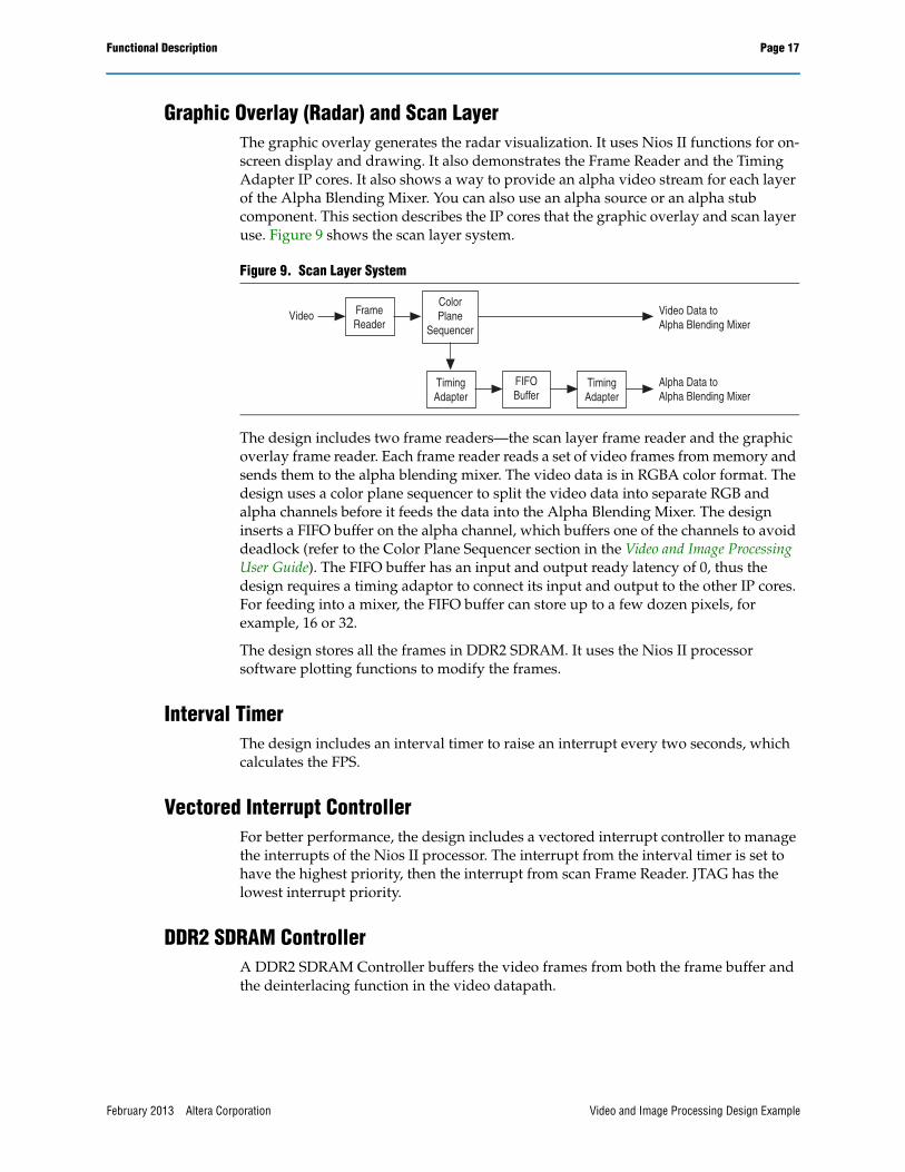
Graphic Overlay (Radar) and Scan LayerThe graphic overlay generates the radar visualization. It uses Nios II functions for on-screen display and drawing. It also demonstrates the Frame Reader and the Timing Adapter IP cores. It also shows a way to provide an alpha video stream for each layer of the Alpha Blending Mixer. You can also use an alpha source or an alpha stub component. This section describes the IP cores that the graphic overlay and scan layer use. Figure 9 shows the scan layer system.
The design includes two frame readers—the scan layer frame reader and the graphic overlay frame reader. Each frame reader reads a set of video frames from memory and sends them to the alpha blending mixer. The video data is in RGBA color format. The design uses a color plane sequencer to split the video data into separate RGB and alpha channels before it feeds the data into the Alpha Blending Mixer. The design inserts a FIFO buffer on the alpha channel, which buffers one of the channels to avoid deadlock (refer to the Color Plane Sequencer section in the Video and Image Processing User Guide). The FIFO buffer has an input and output ready latency of 0, thus the design requires a timing adaptor to connect its input and output to the other IP cores. For feeding into a mixer, the FIFO buffer can store up to a few dozen pixels, for example, 16 or 32.
The design stores all the frames in DDR2 SDRAM. It uses the Nios II processor software plotting functions to modify the frames.
Interval TimerThe design includes an interval timer to raise an interrupt every two seconds, which calculates the FPS.
Vectored Interrupt ControllerFor better performance, the design includes a vectored interrupt controller to manage the interrupts of the Nios II processor. The interrupt from the interval timer is set to have the highest priority, then the interrupt from scan Frame Reader. JTAG has the lowest interrupt priority.
DDR2 SDRAM ControllerA DDR2 SDRAM Controller buffers the video frames from both the frame buffer and the deinterlacing function in the video datapath.
Figure 9. Scan Layer System
ColorPlane
Sequencer
TimingAdapter
FrameReader
FIFOBuffer
TimingAdapter
Alpha Data to Alpha Blending Mixer
Video Data to Alpha Blending Mixer
Video
Video and Image Processing Design ExampleFebruary 2013 Altera Corporation

Page 18 Functional Description
I2C Bus Masters (for Configuration of Video Input and Output Chips)This design instantiates two OpenCore I2C bus masters to enable you to configure both the TVPS154 and TFP410 video interface chips on the HSMC Quad Video and HSMC DVI daughtercards, respectively.
The I2C bus master components provide a convenient interface to configure the video interface chips. An Avalon-MM slave interface receives read and write commands, which the design translates into I2C bus transactions.
The Nios II processor controls the configuration of the video interface chips by writing and reading data to and from the I2C bus master component. The I2C bus masters are not parameterizable through a user interface in Qsys. Altera provides the HDL source code in the local project directory (ip/*).
Debugging SystemThe debugging system allows you to monitor signal data passing between Qsys components and send this data to a host machine running System Console. System Console decodes this data, to provide high-level information about the contents of the signals passing between the components. It also monitors flow control statistics about the connection, allowing you to see how many cycles the design uses to transfer data or to wait for either source or sink to be ready. You can gather this information in real-time from a system over JTAG or USB links. Figure 10 shows the debugging system.
The debugging system comprises two major components: the monitors and the trace system IP core. The design includes monitors in the datapath to capture data. The trace system is the central location to connect all the monitors to and acts as the gateway to the host machine running System Console.
Trace System The trace system transports messages describing captured events from trace monitor components (for example the Avalon-ST Video Monitor) to a host computer running System Console.
You should parameterize the trace system to select the number of monitors that you require. The trace system exposes the capture_n and control_n interfaces. Connect each pair of interfaces to the appropriate trace monitor component. The design has two monitors, with Number of inputs is set to 2, which creates capture_0, control_0, capture_1, control_1. The Bit width of capture interface is the data bus width of the Avalon-ST interface, which sends the captured information. The design has this parameter set to 32 to match this parameterization in the monitors. This design uses the JTAG connection to host.
Figure 10. Debugging System
TraceSystem
Avalon-ST Source (capture)
Avalon-STSource (control)
Monitor 1
Monitor 2
Link to Host
Video and Image Processing Design Example February 2013 Altera Corporation

Functional Description Page 19
The trace system provides access to the control interfaces on the monitors (control_n). You can use these control ports to change capture settings on the monitors, for example to control the type of information captured by the monitors or the maximum data rate sent by the monitor.
When enabled, each monitor sends information about events through its capture interface (capture_n). The trace system multiplexes these data streams. When the trace system runs, it stores them into a FIFO buffer. System Console uses as much bandwidth as possible to stream the contents of this buffer to the host.
The amount of buffering required depends on the amount of jitter inserted by the link. The design uses a buffer size of 16,384 (16 K).
You can add pipeline stages to the design to speed up the system, to give it a greater fMAX. However, adding pipelining increases the amount of logic required in the design. The design uses Insert pipeline stages on all capture inputs.
System Console uses the sopcinfo and .jdi files to discover the connections between the trace system and the monitors. If you use HDL to manually instantiate and connect the trace system and the monitors, System Console can not see them.
MonitorsThe design has monitors in the datapath to capture signals flowing between components. The monitors only tap the wires, and do not use backpressure, so the component cannot stop or stall the flow of data. However, whenever you add any extra component, this addition can affect the Quartus II fitter, and changing the placement of other components can affect timing.
Monitors encapsulate raw data and statistics from the wires that they tap and send this data to the trace system, which forms the data into packets and sends it to the host machine running System Console. You use Qsys to insert the monitor into the datapath between the two components that you want to monitor. For example, to monitor communications between two components A and B that send data via the Avalon-ST protocol, insert an Avalon-ST video monitor into the design that connects A.dout to monitor.din, and monitor.dout to B.din.
Use the control port to control monitors. Every monitor has a register map with common functionality, such as enabling and disabling the monitor from capturing. In addition to these shared functions, monitors can have specific controls relating to their own operation. A capture port also exists in the monitor, which sends the captured data from the monitor to the trace system. Connect both the capture and control ports to the trace system, at capture_n and control_n, respectively.
Connect the clock to the same source that the monitored components connect to. Connect reset from the trace system's reset.
This design uses two Avalon-ST Video Monitors alt_vip_avst_video_monitor_0, connected between my_alt_vip_scl and my_alt_vip_vfb; and alt_vip_avst_video_monitor_1, connected between radar_frame_cpr and my_alt_vip_mix.
They capture the packets of data sent between IP cores and send these encapsulated packets to System Console, which decodes them into accessible visual representations of the packets.
Video and Image Processing Design ExampleFebruary 2013 Altera Corporation
Page 20 Functional Description
The monitors’ parameters must match the values of the IP cores you insert them between. The Bits per pixel per color plane parameter is the number of bits the design requires to represent one part of a color space. For example, a value of 10 when using a color space of RGB means that every pixel requires 10 bits for each red, green and blue color planes, producing a total of 30 bits required for each pixel. If you use the ARGB color space, the design requires 40 bits to represent alpha, red, green, and blue. Number of color planes in parallel and Number of color planes in sequence describe how the video system packs and transfers data between IP cores. The Bit width of capture interface(s) is the width of the data bus from the monitor to the trace system. These values must match.
When you turn on Capture video pixel data, Qsys instantiates hardware that allows monitors to capture pixels from the data packets. You can then look at the contents of the images that are passing between two components, in real time.
For more information about how to see this data, refer to “Setting Up System Console for Debug Visualizations” on page 35.
External DDR2 SDRAM (for Video Buffering)The Altera DDR2 SDRAM Controller controls the data flow to and from the external DDR2 SDRAM. The design uses the controller in half-rate mode, operating at 150 MHz, with a local data interface width of 128 bits. This configuration provides a theoretical maximum available bandwidth of 75×128 = 9.6 Gbps. The design uses the 100-MHz system clock as the PLL reference clock.
Nios II Processor and On-Chip Memory for Program CodeThe Nios II processor initializes and configures multiple video system components, including the I2C external bus masters and the Video and Image Processing Suite IP cores.
The design connects the Nios II Avalon-MM data master to each Avalon-MM slave port it needs access to. Qsys automatically constructs the bus architecture. The system stores the Nios II program code in on-chip memory, with 100 Kbytes of available space.
Nios II processor performs the following functions:
■ Configures the Bitec Quad Video daughtercard video chips (TVP5154 and Chrontel)
■ Configures the Bitec DVI daughtercard video chips (TFP410)
■ Initializes and starts the Video and Image Processing Suite IP cores via the Avalon-MM slave control interfaces
■ Controls the clipper to change the height and width of the clipped video region
■ Controls the scaler output resolution
■ Controls the 2D FIR filter to switch between soft, hard, and edge sharpening
■ Controls the gamma corrector to switch between inverted colors mode and ITU-709 mode
Video and Image Processing Design Example February 2013 Altera Corporation

Functional Description Page 21
■ Controls the mixer:
a. To turn the inputs on and off, flashing them
b. To change the location of the video stream relative to the background layer
The vip_control application project contains a description of the application in the main.cpp file (Figure 11).
The vip_control project includes C++ classes. The C++ classes provide a software API between the Nios II control code and the Video and Image Processing Suite IP cores. The classes provide many member functions to accelerate object-oriented code development and increase visibility of the data flow. For example, the clocked video input class (Clocked_Video_Input.hpp) member functions can report the level in a FIFO buffer in the video system. Or the member functions in the frame buffer class (Frame_Buffer.hpp) can report the number of frames that the Frame Buffer drops or repeats in the datapath.
All Video and Image Processing Suite IP core classes derive from the base class Vipcore.hpp, which contains methods common to all functions such as starting and stopping the video function processing at a frame boundary.
Main FunctionThe main function in main.cpp provides examples of how to use the C++ class member functions to configure and control the datapath functions.
Figure 11. main.cpp in Nios II SBT for Eclipse
Video and Image Processing Design ExampleFebruary 2013 Altera Corporation

Page 22 Functional Description
The main function sets up and initializes all the IP cores at the beginning, then runs the scene script to show the demonstration. At the end, the main function plots the radar and the design enters the main loop to update the radar. The main loop runs forever (unless terminated).
Scene Script
The scene_script function controls the demonstration during each stage. Variable instant states the current time. Different commands are executed at certain time instances. For example:
switch (instant) {
case 100: Turn on DVI input; break;
case 150: Draw text "This is DVI input"; break;
…
}
For some continuous actions, like moving or scaling, keep the time instant at the instant of that command so that this command can be repeated multiple times. Hence variable "transition" states the lack of time instant. Calculate an effective instant by subtracting the transition from the current time instant. For example:
scene loop {
instant++;
effective_instant = instant - transition;
switch (effective_instant) {
case 100: Turn on DVI input; break;
case 150: Draw text "This is DVI input"; break;
case 200:
transition++;
if (transition == 50)
reset transition to 0;
set layer position (x, transition);
break;
case 250: Draw text "This is Composite input"; break;
…
}
}In this design, a moving action occurs at time 200 until time 250. By increasing the transition variable each loop and subtracting it from the instant variable, the effective time instant is kept at 200 until transition reach 50. Thus, the set position command is repeated 50 times, with different parameter value. After that, the time instant continues at 250.
When the whole scene finishes, the function returns false to exit the loop. This scene script is compatible to run within the main loop, so that the control of the video inputs can be run at the same time as other tasks, for example rendering the radar. However, this design does not use it in the main loop.
Video and Image Processing Design Example February 2013 Altera Corporation

System Requirements Page 23
The .hpp files included in the application project allow you to understand the control capability of the Nios II software environment (Figure 12).
System RequirementsThis section describes the hardware and software requirements to run the video design example.
Figure 12. .hpp Files in the Nios II SBT for Eclipse
Video and Image Processing Design ExampleFebruary 2013 Altera Corporation

Page 24 Installing the Design Example
Hardware RequirementsThe Video and Image Processing Design Example requires the following hardware components:
■ Cyclone III Video Development Kit including:
■ Cyclone III EP3C120 host development board
■ Bitec HSMC Quad Video daughtercard
■ Bitec HSMC DVI daughtercard
■ Any NTSC or PAL video source with composite output (such as a DVD player or Apple iPod)
■ Optionally, any video source with DVI output
■ A monitor or display with a DVI interface supporting 1024×768 resolution
■ One DVI cable to connect the DVI output to the monitor
■ Optionally, one DVI cable to connect the DVI video source input to the board
■ Altera USB-Blaster™ cable
Altera used the following hardware to verify the design example:
■ An Apple video iPod (you require an Apple TV out cable to connect the Apple Video iPod to the composite input.)
■ A Sony Handycam HDR-CX150 connected to the composite input
■ An nVidia NVS 300 graphics card connected to the DVI input
Software RequirementsEnsure that you extract the design example .zip file and install the software provided with the development kit.
f For information about the software installation, refer to the documentation provided with the Cyclone III Video Development Kit.
You must install the Quartus II software, version 12.0, which includes the MegaCore IP Library and the Nios II Embedded Design Suite, on your PC.
1 This application note assumes that you install the software into the default locations.
Installing the Design ExampleYou can download the design example files from the Altera Video Processing Reference Design web page. Figure 13 shows the directory structure for the design example files after you extract them from the .zip file.
Video and Image Processing Design Example February 2013 Altera Corporation

Installing the Design Example Page 25
1 Do not use spaces or special characters in the path name.
Table 2 shows the files in the top-level directory:
The Verilog HDL design file contains the following components:
■ Clock source input into phase-locked loop (PLL)
■ PLL megafunction to generate the Qsys system clock and DVI output pixel clocks
■ Input pins for composite input channel 1 (from Bitec Quad Video daughtercard on the HSMC interface J9)
■ Qsys system containing video processing functions
■ DDR2 output pins
■ Output pins system driving DVI output on Bitec HSMC DVI daughtercard (J8)
The Quartus II project also contains pin assignment information for additional interfaces on the Quad Video daughtercard and DVI daughtercard.
Figure 13. Design Example Directory Structure
Table 2. Top-Level Directory Files
File Name Description
alt_vip_reset_recovery.sdc Contains timing constraints for recovery violations
vip_example.jdi JTAG debugging interface file.
vip_example.qpf Quartus II project file.
vip_example.qsf Quartus II settings file.
vip_example.qsys Qsys system file.
vip_example.sof Programming file.
vip_example.sopcinfo System design file.
vip_top.sdc Contains top-level clock requirements
vip_top.tcl Provides full pin assignments for reuse.
<path>Installation directory.
vip_example_design_3c120_<version>Contains files listed in Table 2.
ip
altera_avalon_i2cContains a component (<module name >_hw.tcl and VHDL files) for the I2C controller that communicates with the Bitec Quad Video input card and Bitec DVI input/output card.
software
sourceContains the Nios II C++ source code to configure and control the Clocked Video Input, Clocked Video Output, HSMC daughter card video chips, Clipper, Scaler, Alpha Blending Mixer and Frame Buffer components. There is also a software application program interface in the form of a C++ class for each MegaCore function with an Avalon-MM slave control interface.
Video and Image Processing Design ExampleFebruary 2013 Altera Corporation

Page 26 Opening the Design Example
Opening the Design ExampleThis section describes how to open the Video and Image Processing Design Example. This section includes the following sections:
■ “Opening the Quartus II Top-Level Project”
■ “Opening the Qsys System”
■ “Viewing the Parameters”
■ “Examining and Recompiling the Control Code”
■ “Building the Software in the Nios II SBT for Eclipse”
■ “Debugging the Application Source Code”
You can download the Nios II program, which runs the design example, to the FPGA in one of two ways:
■ Build the binary from the Nios II SBT for Eclipse. Use this flow to understand how to build the software and debug the design example. Continue to “Opening the Quartus II Top-Level Project” on page 26.
■ From a prebuilt binary object file via the Nios II command shell. Use this flow to quickly see the demonstration working on the hardware. Continue to “Downloading vip_control.elf From a Command Shell” on page 35.
1 Altera provide a prebuilt file so you may run the design example directly from the Nios II SBT tools for Eclipse. This method only demonstrates the design example and does not allow you to learn how to build the software or how to debug the design example.
Opening the Quartus II Top-Level ProjectTo open the top-level Quartus II project, perform the following steps:
1. Launch the Quartus II software.
2. On the File menu, click Open Project, browse to <design example install directory>, and select the vip_example.qpf Quartus II project file.
3. On the File menu, click Open, browse to <design example install directory>\top, and select the vip_top.v top-level Verilog HDL design file.
Opening the Qsys SystemTo open the design example Qsys system, with the vip_example.qpf project open in the Quartus II software, click Qsys on the Tools menu.
1 When you launch Qsys, a dialog box displays for you to select the design file. Always select the vip_example.qsys file for this design.
Viewing the ParametersYou can view the parameters of each component, to see what parameters are available to set for customized designs. At this stage, do not change any of the parameters. To view the parameters, perform the following steps:
Video and Image Processing Design Example February 2013 Altera Corporation

Opening the Design Example Page 27
1. In Qsys, in the Name column, double-click my_alt_vip_cti to display the MegaWizard™ interface for the Clocked Video Input (Figure 14).
Table 3 shows the component names to click to view the parameters of each IP core.
Figure 14. Parameter Settings for the Clocked Video Input
Table 3. IP Cores in Design Example IP Cores
Name IP Core
my_alt_vip_clip Composite input Clipper
my_alt_vip_cpr Composite input Color Plane Sequencer
my_alt_vip_crs Composite input Chroma Resampler
my_alt_vip_csc Composite input Color Space Converter
my_alt_vip_dil Composite input Deinterlacer II.
my_alt_vip_clip_1 Composite input Clipper.
my_alt_vip_cpr_0 Composite input Color Plane Sequencer.
my_alt_vip_fir_0 Composite input FIR filter II.
my_alt_vip_cpr_1 Composite input Color Plane Sequencer.
my_alt_vip_scl Composite input Scaler II.
Video and Image Processing Design ExampleFebruary 2013 Altera Corporation

Page 28 Setting Up the Hardware and Configuring the FPGA
Setting Up the Hardware and Configuring the FPGA'This section describes how to set up the Cyclone III video Development Board and configure the Cyclone III device.
1 The top-level vip_top.v file includes quick start instructions.
alt_vip_avst_video_monitor_0 Avalon-ST Video Monitor.
my_alt_vip_vfb Composite input Frame Buffer.
my_alpha_source Composite input Alpha Source.
my_alt_vip_tpg Test Pattern Generator.
tpg_alpha_stub Alpha Stub.
my_alt_vip_mix Alpha Blending Mixer.
my_alt_vip_itc Clocked Video Output.
altmemddr DDR2 SDRAM Controller.
dvi_in_alt_vip_cti DVI input Clocked Video Input
dvi_in_alt_vip_clip DVI input Clipper
dvi_in_alt_vip_cl_scl DVI input Scaler II.
dvi_in_alt_vip_gam DVI input Gamma Corrector.
dvi_in_alt_vip_vfb DVI input Frame Buffer.
dvi_in_alpha_source DVI input alpha source.
scan_cpr Scan layer Color Plane Sequencer.
scan_sc_fifo Scan layer Avalon-ST Single Clock FIFO buffer.
scan_timing_adapter_0 Scan layer Avalon-ST Timing Adapter.
scan_timing_adapter_1 Scan layer Avalon-ST Timing Adapter.
scan_vfr Scan layer Frame Reader.
radar_frame_vfr Graphic overlay Frame Reader.
radar_frame_cpr Graphic overlay Color Plane Sequencer.
alt_vip_avst_video_monitor_1 Avalon-ST Video Monitor.
radar_frame_timing_adapter_0 Graphic overlay Avalon-ST Timing Adapter.
radar_frame_sc_fifo Graphic overlay Avalon-ST Single Clock FIFO buffer.
radar_frame_timing_adapter_1 Graphic overlay Avalon-ST Timing Adapter.
trace_system_0 Trace System.
Table 3. IP Cores in Design Example IP Cores
Name IP Core
Video and Image Processing Design Example February 2013 Altera Corporation

Setting Up the Hardware and Configuring the FPGA Page 29
Setting Up the Cyclone III Video Development PlatformFigure 15 shows the hardware setup.
To set up the Cyclone III development board, perform the following steps:
1. Ensure you disconnect the power cable from the Cyclone III development board.
2. Connect one end of the USB-Blaster cable to the USB port on your PC.
3. Connect the other end of the USB Blaster cable to the 10-pin header labeled (JTAG) on the Cyclone III development board.
4. Connect the Bitec HSMC Quad Video daughtercard to HSMC interface port B (J9) on the Cyclone III development board.
Figure 15. Cyclone III Development Board Hardware Setup
Video and Image Processing Design ExampleFebruary 2013 Altera Corporation

Page 30 Setting Up the Hardware and Configuring the FPGA
5. Connect the video source composite input cable to the top left input connector (J10) on the Bitec Quad Video daughtercard (Figure 16).
6. Connect the Bitec HSMC DVI video daughtercard to the HSMC interface port (J8) on the Cyclone III development board.
7. Connect one end of the DVI cable to a DVI monitor, capable of 1024×768 @ 60Hz. Connect the other end to the TX connector on the Bitec DVI daughtercard.
8. Connect one end of the second DVI cable to a suitable DVI input video source. Connect the other end to the RX connector on the Bitec DVI daughtercard.
9. Connect the power cable to the Cyclone III development board.
10. Locate the switch on the board located close to the port for the power cable. Change the switch to the On position so that the LED labeled POWER illuminates.
f For details about installing the USB Blaster software driver on the host PC (located at <quartus_install_dir>\drivers\usb-blaster), refer to the USB-Blaster Download Cable User Guide.
f For details about the Cyclone III DSP development board, refer to the Cyclone III Development Board Reference Manual.
Configuring the Cyclone III DeviceTo configure the Cyclone III device, download the vip_example.sof file to the development board by following these steps:
1. In the Quartus II software, on the Tools menu, click Programmer.
2. On the File menu, click Save As.
3. Navigate to the design installation directory, and in the Save As dialog box, type vip_top.cdf in the File Name box.
4. In the Save as type list, select Chain Description File.
Figure 16. Composite Video Connection to Quad Video Daughtercard
Video and Image Processing Design Example February 2013 Altera Corporation
Using Nios II SBT for Eclipse Page 31
5. Click Save.
6. In the Programmer window, select JTAG in the Mode list.
7. Click Hardware Setup to configure the programming hardware. The Hardware Setup dialog box appears.
8. In the Hardware column, click USB Blaster.
9. In the Currently select hardware, select USB-Blaster.
10. Click Close to exit the Hardware Setup dialog box.
11. Click Add file, browse to the design installation directory, click vip_example.sof, and click Open.
12. Turn on Program/Configure for vip_example.sof.
13. Click Start.
The Programmer begins to download the configuration data to the FPGA. The Progress field displays the percentage of data that downloads. A message appears when the configuration is complete.
1 If you do not use a licensed version of the Video and Image Processing Suite, a message appears indicating that you are running a time-limited configuration file on your target hardware.
Using Nios II SBT for EclipseThis section describes how to use Nios II SBT for Eclipse with the design.
Examining and Recompiling the Control CodeTo use the Nios II SBT for Eclipse to examine and recompile the Nios II C++ control code and associated board support package (BSP), perform the following steps:
1. On the Windows Start menu, point to All Programs, point to Altera, point to Nios II EDS <version>, and then click Nios II <version> Software Build Tools for Eclipse. The Workspace Launcher dialog box appears.
2. Select a workspace folder by browsing to the design example \software directory and specifying a workspace subdirectory. For example, <install directory>\software\workspace.
3. Click OK to create a new workspace.
4. On the File menu, point to New, and then click Nios II Application and BSP from Template. The Nios II Application and BSP from Template dialog box appears.
5. From the SOPC Information File name box, browse to the vip_example.sopcinfo file. The Nios II SBT for Eclipse fills in CPU name with the processor name found in the .sopcinfo file.
6. In the Project name box, type vip_control.
Video and Image Processing Design ExampleFebruary 2013 Altera Corporation

Page 32 Using Nios II SBT for Eclipse
7. Select Blank Project from the Templates list (Figure 17) and then click Next.
8. Select Create a new BSP project based on the application project template.
9. Accept the default project name, vip_control_bsp.
10. Ensure that Use default location is turned on.
11. Click Finish to create the application and the BSP based on the vip_example.sopcinfo file.
12. After the BSP generates, the vip_control and vip_control_bsp projects appear in the Project Explorer view.
13. In Windows Explorer, navigate to design’s software\source directory.
14. Select all 51 C++ VIP IP files and drag them onto vip_control in the Nios II SBT for Eclipse Project Explorer view to include them in the project.
1 Ensure that you drag the files into the vip_control project, and not the vip_control_bsp project.
Figure 17. Nios II Application and BSP from Template Dialog Box
Video and Image Processing Design Example February 2013 Altera Corporation

Using Nios II SBT for Eclipse Page 33
Building the Software in the Nios II SBT for EclipseTo build the software in the Nios II SBT for Eclipse, perform the following steps:
1. Before building the vip_control_bsp project, reduce memory footprint:
a. Right-click vip_control_bsp in the Project Explorer view, and click Properties. The Properties for vip_control_bsp dialog box appears.
b. Click Nios II BSP Properties.
c. Turn on Reduced device drivers and Small C library, and ensure that Support C++ is turned on.
d. Click OK. The vip_control_bsp project regenerates.
2. Before building the vip_control project:
a. Right-click vip_control_bsp in the Project Explorer view, point to Nios II, and then click BSP Editor. The Nios II BSP Editor dialog box appears.
b. Select the Linker Script tab at the top of this dialog, and look at the table named Linker Section Mappings.
c. For .bss, .rodata, .rwdata, .stack and .text set the Linker Region Name set to onchip_mem.
d. Also make sure that the .heap entry has the Linker Region Name set to altmemddr.
e. Click Generate.
f. Click Exit.
3. Right-click vip_control in the Project Explorer view, point to Run as, and then click Nios II Hardware. The Nios II SBT for Eclipse compiles the vip_control_bsp and vip_control software projects and builds the vip_control.elf software executable. After the build stage completes, the Run Configurations dialog box appears.
4. Verify that vip_control is in the Project name box, and the newly created vip_control.elf file is in the ELF file name box.
5. Click the Target Connection tab, and then click Refresh Connections.
6. Verify that the USB-Blaster and EP3C120 configuration device appear under Connections.
Running the Nios II Control ProgramTo run the Nios II control program, perform the following steps:
1. Click Run. Log information appears in the Nios II Console output including the following log:
Composite input F0 width x height= 720 x 244
Composite input F1 width x height= 720 x 243
2. Verify that the design starts and displays text on the screen that guides you through the demonstration of the various functions.
Video and Image Processing Design ExampleFebruary 2013 Altera Corporation

Page 34 Using Nios II SBT for Eclipse
3. You can rebuild, edit, and debug the control code in the Nios II SBT for Eclipse with the software API classes provided to access the Video and Image Processing Suite functions.
You have successfully completed the Video and Image Processing Design Example demonstration.
Debugging the Application Source CodeTo debug the application source code, perform the following steps:
1. Right-click vip_control, point to Debug As, and then click Nios II Hardware.
1 A message asking you if you want to switch perspective might appear. Clicking Yes switches to the debug perspective view. The VIP hardware stops manipulating the video, and the program pauses at the start of the main() function.
2. Insert a breakpoint by clicking in the margin next to the following line (Figure 18):
while (!vfr_frame_finished) {};
3. Right-click and click toggle breakpoint.
4. Click Resume to run the initialization code. The program runs through the video input demonstration and breaks at the clip(the_progressive_clipper); while (!vfr_frame_finished) {}; line, just after the radar display appears.
5. Click Resume again and notice scan line and enemies on the radar view move by an increment. The program breaks at the while (!vfr_frame_finished) {}; line again.
1 In a debug session, you can perform many debug operations including breakpoint insertion, viewing registers, viewing memory data, viewing variables, and single stepping instructions.
6. To end the debug session, click Terminate.
Figure 18. Inserting a Breakpoint in the Nios II Debug Window
Video and Image Processing Design Example February 2013 Altera Corporation

Setting Up System Console for Debug Visualizations Page 35
f For more information about running a Nios II debug session, refer to “Getting Started” in the Getting Started with the Graphical User Interface chapter of the Nios II Software Developer’s Handbook.
Downloading vip_control.elf From a Command ShellYou may download the .elf file from a command shell, but you cannot then debug the design example. To download, perform the following steps:
1. Complete all of the sections in “Setting Up the Hardware and Configuring the FPGA” on page 28.
2. Start a Nios II Command Shell (On the Windows Start menu, point to Programs, then Altera, then Nios II EDS <version>, and click Nios II <version> Command Shell).
3. Change the directory to <design example install> /vip_example_design_3c120_<version>.
4. Download the vip_control.elf file and start the Nios II terminal window to display print output using the command:
nios2-download -g -r vip_control.elf; nios2-terminal
The resolutions of the input video fields (F0 and F1) display in the Nios II terminal window and a video stream appears on the screen.
Setting Up System Console for Debug VisualizationsTo set up the development board and host computer to use the trace system with System Console for debugging, follow these steps:
1. In Eclipse, right-click vip_control, point to Debug As, and then click Nios II Hardware.
1 A message asking you if you want to switch perspective might appear. Click Yes to switch to the debug perspective view. The software running on the Nios II processor stops controlling the VIP cores and the program pauses at the start of the main() function.
2. Find the following section of main.cpp:
case START_COMP + 620:
// Scale up the composite video
if (transition > 70) {
transition = 0;
} else {
transition++;
comp_scaler.stop(true);
comp_scaler.set_output_size((int)(((float)transition/100.0+1.0)*360.0), (int)(((float)transition/100.0+1.0)*240.0));
comp_scaler.start();
Video and Image Processing Design ExampleFebruary 2013 Altera Corporation

Page 36 Setting Up System Console for Debug Visualizations
}
break;
3. Insert a breakpoint by clicking in the margin next to the line:
"if (transition > 70) {"
This breakpoint stops the debugger when it reaches the point in the program where it is scaling up the composite input.
4. Click Resume to run the initialization code. The program runs through the video input demonstration until it breaks just before it starts to scale the composite video input. While the Nios II code is suspended, the composite video path is unaffected, and continues to display live video from the input source, because the Nios II processor only controls the parameters of the VIP IP cores. Suspending the code does not affect the operation of the VIP IP cores.
5. Leave Nios II SBT for Eclipse at this breakpoint while you start System Console.
6. Open System Console. In Qsys, on the Tools menu, select System Console.
7. Under System Explorer, expand designs and expand vip_example.qpf (Figure 19). If you cannot expand designs, perform one or both of the following steps:
■ Click on File, then click Load Design… and navigate to the vip_example.qpf file.
■ Expand devices, right-click on the part number for the Cyclone development board EP3C120|EP4CE115. and select Link device to, then click on vip_example.qpf.
Figure 19. System Console
Video and Image Processing Design Example February 2013 Altera Corporation

Setting Up System Console for Debug Visualizations Page 37
8. On the Tools menu select Trace Table View. The Capture Settings dialog box appears.
1 This option only appears with projects that contain a trace system.
9. In the Select Hardware drop-down box select devices/EP3C120|EP4CE115…. A table appears that displays options. The first three options are for the monitors that are present in the system alt_vip_avst_video_monitor_0 and alt_vip_avst_video_monitor_1. The last option controls how large the database is within memory, which controls how many events System Console can capture at any one time before discarding the oldest captured events.
10. In the Value column, specify the following options (Figure 20), and then click OK:
■ For alt_vip_avst_video_monitor_0 Capture Rate per 1000000, change how many pixels the monitor captures from each data packet (“The Capture Rate Value” on page 39).
■ For alt_vip_avst_video_monitor_0 Enable, select Enable with pixel capture, to capture pixels and allow you to view the contents of video data packets.
■ Turn on alt_vip_avst_video_monitor_1.
1 The two monitor settings are different because you turned on Capture video pixel data in the Qsys parameters for the alt_vip_avst_video_monitor_0 monitor.
1 You can access this dialog box anytime by clicking on the spanner icon in the top left of the Trace Table View tab.
11. Click the Start icon to start capturing data. The table fills up with events. The data that System Console sends between IP cores is in packets. The packets have the following general order:
■ Video control packet, which details resolution and format
■ Video data packet, which contains the actual video data to display.
12. Click the Pause icon to temporarily halt the current display, which allows you to view a snapshot of the captured data while System Console continues to collect new events in the background.
13. Select a video control packet from the table and then expand Video control, Statistics, and Data in the bottom area of the trace table tab. System Console displays high-level decoded information about this packet: the decoded information within the packet (width, height and format data), the statistics about the connection (the number of cycles spent performing certain tasks), and the raw data contained in the packet.
Figure 20. Monitor Settings
Video and Image Processing Design ExampleFebruary 2013 Altera Corporation

Page 38 Setting Up System Console for Debug Visualizations
14. Select a video data packet from alt_vip_avst_video_monitor_0.
a. Expand the data and pixel capture nodes to show a reconstruction of the captured pixels from this data packet. As the capture rate per frame is typically only a few hundred pixels, the reconstruction algorithm can make the image appear blurred, but it is a good indication of the content of that data packet.
b. Expand the save node to see the raw captured pixel data.
c. Look at the number of pixels captured per frame (“The Capture Rate Value” on page 39).
15. Click the Pause icon again to unpause the table, and then click on the Filter Monitors icon. A menu appears that allows you to show and hide monitors, but still have them capture data in the background.
16. Turn off trace_system_0_tracesys.capture_1, which corresponds to the component alt_vip_avst_video_monitor_1 (indicated in the Path column). Click Close and only one monitor now displays.
1 If the trace table view scroll bar moves to the top of the screen as it tracks the packet, drag the scroll bar to the bottom of the screen to lock it and show the latest incoming packets.
17. Enter Video Data in the RegEx Filter text box. The filter just shows video data packets.
1 The RegEx filter is case-sensitive.
18. View the captured video pixel data as it arrives into the system.
Figure 21. Hierarchical View of the Data Packet
Video and Image Processing Design Example February 2013 Altera Corporation

The Capture Rate Value Page 39
19. Open the Nios II SBT for Eclipse window next to the System Console window, to see them simultaneously. The Nios II SBT for Eclipse is still paused on the breakpoint.
20. Press Resume to move the program one step forward and scale the image on the screen up by an increment. Each time you press Resume, the resolution of the packets in System Console Trace Table View increases. The resolutions starts at 360x240 and increases by around three pixels in each dimension with every increment of the Nios II program. This action demonstrates the System Console trace system working with the Nios II debugger. It also shows the trace system debugging designs that use the Video and Image Processing Suite IP cores.
The Capture Rate ValueYou can specify the Capture rate per 1000000 value for every monitor that captures video pixel data.
The value depends on:
■ The size of the image
■ The number of frames per second at which the video system runs
■ The available bandwidth of the debug link
Typically, over a JTAG link and viewing a datapath that runs at 60 frames per second, you can capture a few hundred pixels per frame. The value you enter for Capture rate per 1000000 depends mainly on your image size. For example, for a 25×20 pixel video stream, enter 1000; for a 1920×1080 pixel video stream, enter 500. Then run the system and view the output. At anytime, you can stop the trace system, adjust the value, and restart the trace system.
If the value is too small, the pixel capture view does not have enough data to create a meaningful picture. If the value is too large, the system does not have not enough bandwidth to send all the captured pixels and it displays a black and purple checkerboard pattern. Adjusting the value allows you to see a representation of the image that the data packet contains.
Applications for the Design ExampleMany new video innovations, such as HDTV and digital cinema, involve video and image processing and this technology's rapid evolution. Leaps forward in image capture and display resolutions, advanced compression techniques, and video intelligence are the driving forces behind the technological innovation.
Figure 22. Setting Capture Rate Values
Video and Image Processing Design ExampleFebruary 2013 Altera Corporation

Page 40 Applications for the Design Example
The move from standard definition (SD) to high definition (HD) represents a six times increase in data processing requirements. Video surveillance is also moving from common intermediate format (CIF) (352×288) to D1 format (704×576) as a standard requirement, with some industrial cameras moving to HD (1280×720). Military surveillance, medical imaging, and machine vision applications are also moving to very high resolution images.
With expanding resolutions, you need high-performance designs while keeping architectures flexible to allow for quick upgradeability.
All Altera Video and Image Processing Suite IP cores are configurable to allow you to satisfy common performance and cost requirements over a wide range of SD and HD resolutions. This section describes some of the many video systems that you construct with the Video and Image Processing Suite IP cores.
Single Video Stream InputThe design example is a good starting point for developing single input or multiple input video stream applications. The design example demonstrates how to construct a video datapath that performs deinterlacing, clipping, chroma resampling, finite impulse response (FIR) filtering, gamma correction, color space conversion, mixing and scaling.
The Altera Video and Image Processing IP cores all have common data and control interfaces. These common interfaces, and open protocol for transmitting video, make it easy to extend the datapath in the design example to perform additional video processing functions.
The design example also demonstrates how to use a Nios II processor to configure and control the video interface chips, clocked video input, clocked video output, frame buffer, and image mixer. The standardization on Avalon-MM control interface ports makes the Nios II processor a convenient choice for run-time control, enabling a rapid development cycle in a software environment.
You can enable the run-time control interfaces on video processing functions, such as the Test Pattern Generator and Color Space Converter, and add new functions. You can enable these Avalon-MM slave control ports from the MegaWizard interfaces. When Qsys regenerates and the Quartus II software recompiles the hardware system, control of the system is in the software domain.
The IP core register maps provide both control and visibility of the data flowing in the datapath. For example, you can perform the following actions:
■ Perform real-time changes to the size of the test pattern stream.
■ Update the scaling coefficients to improve image quality at run-time.
■ Change the Color Space Converter coefficients at run-time.
■ Track the number of frames that the frame buffer drops or repeats due to data rate transitions.
■ Monitor the number of words in the dual clock FIFO of the Clocked Video Input and Clocked Video Output IP cores, to track overflow and underflow or peak FIFO usage.
Video and Image Processing Design Example February 2013 Altera Corporation

Applications for the Design Example Page 41
Multiple Video Channel InputVideo systems frequently contain multiple video streams, which process in parallel and are synchronized. Altera’s Video and Image Processing IP cores are suitable for constructing video systems with small numbers of channels (such as converter boxes) up to systems with hundreds of video streams (such as switchers and multiviewers).
Use the 3C120 Video Development Kit to easily extend the design example. It can support four composite or S-Video video stream inputs via the Bitec HSMC Quad Video daughtercard, and the DVI input on the Bitec HSMC DVI daughtercard.
The Nios II software allows you to configure the TVP5154 chip on the Bitec HSMC Quad Video daughtercard for four composite inputs.
To extend the design example to support additional composite input video streams, follow these steps:
1. In Qsys, create an additional video processing data pipeline to input into the mixer, with the processing functions (Figure 23).
1 You must ensure that the video functions process data at the required rate to avoid overflow at the input of the system and underflow at the output. When adding functions to a system that connect to external memory, such as a deinterlacer, ensure that there is sufficient external memory bandwidth available.
2. Increase the number of inputs to the Alpha Blending Mixer.
3. Connect the new data pipeline to the new mixer input.
4. Regenerate the Qsys system.
5. Instantiate the new Qsys symbol in the top-level Quartus II .v file, add the appropriate Bitec Quad Video card input pins (the project already contains the correct assignments), connect the exported wires from the Qsys system to the new input pins, save the .v file, and recompile the Quartus II project.
6. Update the software project to initialize and control the mixer.
Multiple input stream systems raise many challenges, such as achieving the required level of external memory bandwidth, often with a shared DDR external memory; synchronizing multiple streams of video at different data rates; or processing at HD data rates. Altera is continuously developing the framework to simplify such system and design challenges.
Other Video Interface StandardsThe design example allows you to develop video systems with NTSC, PAL or DVI video input and DVI video output. This design example requires appropriate hardware ports on the video development board, analog-to-digital conversion and FPGA hardware interface components.
Figure 23. Qsys Processing Functions
FrameBuffer
ClockedVideoInput
ClipperChroma
ResamplerScalerDeinterlacer
Video and Image Processing Design ExampleFebruary 2013 Altera Corporation

Page 42 Applications for the Design Example
You see a variety of different hardware interface standards and protocols in applications throughout the broadcast, consumer, automotive, surveillance, medical, and document imaging markets. These standards include high definition multimedia interface (HDMI), component, S-Video or Y/C (with separate luminance and color signals), SDI, high definition SDI (HD-SDI) and 3GBit/s SDI (3G SDI).
Programmable FPGAs are ideal for migrating systems that support different interfaces. You can use the design example as a framework for development of such FPGA hardware interface components. You can reparameterize the Clocked Video Input and Clocked Video Output IP cores in the Qsys system to match the video format and adapting the top-level design with the appropriate video interface and pin assignments.
For example, you can develop video systems with SDI video input and output ports that use the Stratix® II GX board and the Altera SDI/HD-SDI IP core by applying the same video framework methodology that this design example uses.
Extending the Graphic Overlay You can use and extend the graphic overlay that the design example uses to display the radar for other purposes. This section gives a brief overview of how major parts of the system interact, and how to use the available functions.
The design uses double buffering to update the scan layer in the main loop. The frame reader raises an interrupt to update the state variable every time the design reads a complete frame. The procedure of the main loop is:
1. Update scan line.
2. Update enemy system, remove and plot the enemies on the screen.
3. Create new enemy if necessary.
4. Switch current frame (no effect until frame reader finishes transferring current frame).
5. Wait until state variable is set by the interrupt.
6. Go to step 1.
Scan Line DrawingThe design moves the scan line around the center of the radar, hence a straight line is drawn from the center to a point on the edge. To reduce run-time floating point and trigonometry operations, the design precalculates the edge points and store them in a look-up table (LUT). The table only stores 1/8 of all the possible values, and maps to the full domain using the function:
void get_scan_coordinate(int angle, int &x, int &y)
The design also uses the look up table for generating enemies on the boundary.
The design plots the scan line with the same technique as the enemy system—it removes the previous line by drawing a same line with transparent color.
Video and Image Processing Design Example February 2013 Altera Corporation
Applications for the Design Example Page 43
Time Interval Interrupt FPSThe system consists of an interval timer, which raises an interrupt every two seconds and resets the frame counter. At the same time, the design derives the FPS by the number of frames it counts since the last reset, and plots the FPS on the top layer of the scene.
Input DetectionThe design checks both the composite and DVI inputs during the main loop. The design detects and displays any new connection on the screen during run time.
Class Screen_displayThe class screen_display is a preliminary class for implementing the plot. The design transfers the plot commands into point position and values, and then the design writes to the screen frame stored in the memory. The frame reader reads the frame and the design sends it to the next steaming sink in the system (in this example it is the Alpha Blending Mixer).
Each pixel value is in RGBA format with 8-bits per color (a whole 32-bit word). The frame reader reads data in words and wastes no bytes during the transfer.
Other than the setup function, the design has two sets of plot functions: the basic drawing functions and screen map drawing functions.
Basic Drawing FunctionsThe basic drawing functions directly access the memory, which is convenient for simple shapes like point, line, square, rectangular, circle and arc. It is not suitable for plotting solid objects. The line and circle function use Bresenham's algorithm and thus no multiplication, division or floating point operations are required.
The design draws text with the line drawing functions. The size set affects the appearance of the text, which appears better when using smaller font sizes. Also, because the design does not write memory access in text drawing to consecutive addresses, for large amount of text drawing, the efficiency is generally low.
Screen Map Drawing FunctionsA screen map is a list of lines on the screen, storing only the start and end node of any shape added into the list. It is suitable for drawing solid shapes, including squares, rectangles, circle, arcs and other non-standard shapes. The design supports any single border shape but they may not be as efficient as using direct drawing.
During initialization, the design creates the list with a header node for each line. To reduce memory usage, you can use a list of node pointers instead of header nodes, which complicates the program.
If you use the draw_***_sm function to add any shape, the design interprets it as a left and right node pair stored in the screen map list. To insert inverse shapes, shapes (removing a partition area from an existing shape), insert a left and right pair in reverse order. To add non-pair drawing (a shape without either left or right border) , use the brd_single option. The design stores all the shapes in the list, and writes them to the memory when you call the draw_screen_map(int frame_index) function. Use the clear_screen_map() function to release the memory.
Video and Image Processing Design ExampleFebruary 2013 Altera Corporation

Page 44 Applications for the Design Example
Available Functions/************************************************
*
* Setup function
*
***********************************************/
Screen_Display(long frame_address_0, long frame_address_1=-1)
~Screen_Display()
void set_frame_size0(int frame_width, int frame_height)
void set_frame_size1(int frame_width, int frame_height)
void initial_screen_map(int sm_width, int sm_height)
void set_screen_map_position(int x, int y)
/**********************************************
*
* Basic drawing function
*
*********************************************/
void set_pixel(int frame_index, int x, int y, int pixel_colour=-1)
void set_pixel_blend(int frame_index, int x, int y, int red=-1,
int green=-1, int blue=-1, int alpha_value=-1)
void set_colour(int red, int green, int blue, int alpha_value=0)
void set_colour(int colour_RGB_ALPHA)
int get_colour()
void clear_screen(int frame_index=0, int clear_colour = 0xFF000000)
void draw_line(int frame_index, int x0, int y0, int x1, int y1) {
void draw_square(int frame_index, int x0, int y0, int x1, int y1)
void draw_rectangular_align(int frame_index, int x0, int y0,
int x1, int y1, int thickness)
void draw_test_pattern(int frame_index=0, int alpha=0x80)
void draw_circle(int frame_index, int x0, int y0, int radius)
void draw_arc(int frame_index, int x0, int y0, int radius,
int angle_start, int angle_end)
void draw_text(int frame_index, char str[], int x, int y, int size)
Video and Image Processing Design Example February 2013 Altera Corporation

Applications for the Design Example Page 45
/*********************************************************
*
* Screen map function
*
* ============== Warning ===============
* Screen map function are not fully tested. To keep the full
* flexibility that user could have, leave a few known constrains.
*
********************************************************/
void draw_screen_map(int frame_index)
void clear_screen_map()
void release_screen_map()
void print_screen_map()
void validate_screen_map()
void remove_duplicated_screen_map(int y0, int y1)
void set_pixel_sm(int frame_index, int x, int y, int pixel_colour=-1)
void draw_line_sm(int x0, int y0, int x1, int y1)
void draw_line_bresenham(int x0, int y0, int x1, int y1,
int border_property)
void draw_square_sm(int x0, int y0, int x1, int y1, int invert=0)
void draw_border_sm(int border_width=1)
void draw_circle_sm(int x0, int y0, int radius, int invert=0)
void draw_ring_sm(int x0, int y0, int radius0, int radius1){
void draw_arc_sm(int x0, int y0, int radius, int angle_start,
int angle_end, int invert=false).
Class Gamma_Corrector
The design adds the void init_itu709_8_decode(float power, float offset) ITU-709 gamma decode function into the gamma_corrector class, to implement the following function:
following function:
where:
■ L is the luminance of the image 0 ≤ L ≤1
■ V is the corresponding electrical signal
Video and Image Processing Design ExampleFebruary 2013 Altera Corporation

Page 46 Applications for the Design Example
This function emphasizes the mid-range value for all colors. The design includes an offset and domain scale to adjust the black and white level. The design precalcualtes this function at the first function call, and stores it in a lookup table for later use.
Class FIR_2D_Filter
The class FIR_2D_Filter contains some preliminary functions for setting up the coefficients for the 2D-FIR filter:
FIR_2D_Filter(long base_address, unsigned int size, unsigned int frac_bits)
void init_coef_matrix(float* coefficient)
void init_coef_matrix_sym(float coefficient[])
The init_coef_matrix_sym function supports symmetric coefficients. The argument coefficient expects coefficients in a center-to-edge order. For example, a 7x7 matrix arranges coefficients in the following order:
9 8 7 6 * * *
* 5 4 3 * * *
* * 2 1 * * *
* * * 0 * * *
* * * * * * *
* * * * * * *
* * * * * * *
The program creates the other symmetric coefficients.
The design includes a sharpening effect. You should keep the absolute value of the sum of all surrounding coefficients to be exactly 1 less than the center coefficient. The greater the difference between the center and each surrounding coefficient, the harder the sharpening effect is. In some cases set the sum to be the same as the center value (but with the opposite sign), to obtain a black-and-white edge only image.
Class Enemy_Sys
The class enemy_sys simulates enemy objects in the radar model. It maintains a list of enemies, updates each frame and uses the on-screen display functions to plot them on the screen.
The frame that the design initially draws class enemy_sys to is transparent. However, when performing dynamic drawing, you must clear the object that the design plots in the preceding frame. It should be the frame before last, because the design uses double-buffering. Clearing the whole screen costs bandwidth. The design uses the same previous plot, but with a transparent color, which removes what the system draws in the frame before last.
The class enemy_sys includes the following functions:
Enemy_Sys(Screen_Display* the_screen_writer, int centre_x, int centre_y){
~Enemy_Sys()
void init_enemy_sys(int max_distance_from_center, float enemy_min_speed,
float enemy_max_speed, int reflash_life_increment,
Video and Image Processing Design Example February 2013 Altera Corporation

Conclusion Page 47
unsigned int highlight_colour, unsigned int dim_colour,
int colour_step_num)
void create_enemy(int x, int y, int angle, int init_life)
void refrash_enemy(int current_frame, int angle)
void remove_dead_enemy()
void plot_list(int current_frame, bool is_remove)
void plot_node(Enemy* plot_node, int current_frame, bool is_remove)
int get_enemy_num()
float sign_of_num(float num)
To reduce oscillation the design performs the coordinates and speed calculation in the floating point domain.
ConclusionThe Video and Image Processing Design Example demonstrates a reusable and flexible video framework for rapid development of video and image processing designs. The design uses standard open interfaces and protocols throughout the system. You can reuse parameterizable IP cores from the Altera MegaCore IP Library (which includes the Video and Image Processing Suite) or add your own IP to the framework to build further applications.
The design implements system control code in software that runs on a Nios II processor, which provides a rapid edit debug cycle. A C++ class based software API provides an interface to the Video and Image Processing Suite IP cores from the Nios II control software to ease software development.
The video framework does not preclude using HDL to connect the IP components. However, the design example demonstrates that the Qsys environment significantly accelerates system design by:
■ Providing automatic generation of an application-specific switch fabric including arbitration scheme
■ Providing an abstracted view of the video system
■ Detecting and displaying Altera and user IP in an immediately accessible form
Revision HistoryTable 4 shows the revision history for the AN-427: Video and Image Processing Design Example application note.
Table 4. AN-427 Revision History (Part 1 of 2)
Version Date Change Summary
10.2 February 2013 ■ Corrected screen shot.
10.1 February 2013■ Updated for the Quartus II software version 12.1
■ Added capture video pixel data feature
Video and Image Processing Design ExampleFebruary 2013 Altera Corporation

Page 48 Revision History
10.0 July 2012
■ Updated for the Quartus II software version 12.0
■ includes a DVI input
■ Uses the Nios II processor to create a graphical overlay display of a radar
■ Includes debugging components
■ Adds the following IP cores:
■ Gamma corrector
■ 2D FIR Filter
■ Alpha sources
■ Frame readers
■ Timing adaptors
■ Avalon-ST Video monitors
■ Trace system
9.0 June 2011Updated for Qsys version 11.0, new MegaWizard interface, new Deinterlacer II MegaCore and Scaler II IP cores in the Video and Image Processing Suite, and minor changes to the design example.
8.1 July 2010 Updated for SOPC Builder version 10.0, new MegaWizard interface, new Interlacer IP core in the Video and Image Processing Suite, and minor changes to the design example.
8.0 November 2009 Updated for Nios II SBT for Eclipse, SOPC Builder version 9.1, Quartus II software version 9.1, new Video and Image Processing Suite IP cores, and minor changes to the design example.
7.0 March 2009 Updated for Quartus version 9.0. The OpenCores I2C Master warning message errata is fixed and the Clocked_Video_Input.hpp status register API is corrected.
6.1 January 2009 Minor corrections.
6.0 December 2008Updated for Quartus version 8.1. Revised design that uses run-time control of the Clipper, Deinterlacer, Scaler, and Frame Buffer IP cores and supports PAL video as an alternative to NTSC.
5.0 July 2008Updated for Quartus version 8.0. Completely revised design for using the Cyclone III Video Development kit with Bitec HSMC daughtercards. The design example is implemented by IP cores instantiated in SOPC Builder with control provided by a Nios II processor.
4.0 October 2007Updated for Quartus version 7.2. The design now uses DSP Builder Video Source and Video Sink blocks and the triple buffer block is replaced by a Frame Buffer IP core. Removed obsolete troubleshooting issue “Compilation Fails in Analysis and Synthesis”.
3.0 May 2007 Updated for Quartus version 7.1.
2.0 December 2006 Updated for Quartus version 6.1.
1.2 July 2006 Added troubleshooting issues “Compilation Fails in Analysis and Synthesis” and “DDR2 Fails in Analysis and Synthesis or In Timing Analysis”.
1.1 July 2006 Updated algorithm used by the triple buffer block, effects of VGA starvation, description of the image stream frame counter block, and other minor edits.
1.0 June 2006 First release of this application note.
Table 4. AN-427 Revision History (Part 2 of 2)
Version Date Change Summary
Video and Image Processing Design Example February 2013 Altera Corporation