viewed - nasa · object system as viewed by a moving observer ... working i reg 530 i 1 i' i i...
TRANSCRIPT

United States Patent [191
Lotz et al. 11 11 4,208,719 [45] Jun. 17, 1980
EDGE SMOOTHING FOR REAGTIME SIMULATION OF A POLYGON FACE OBJECT SYSTEM AS VIEWED BY A MOVING OBSERVER Inventors: Robert W. btz, Santa Cruz; David J.
Westerman, San Jose, both of Calif.
Assignee: The Singer Company, Binghamton, N.Y.
Appl. No.: 933,255 Filed: Aug. 10, 1978 Int. Cl.2 ................................................ CO9B 9/08 U.S. Cl. ................................... 364/515; 35h0.24;
340/728; 358/160; 364/521; 364/578 Field of Search ............... 364/515, 555, 522, 521,
364/578; 358/166, 103, 104, 135, 160; 35A0.2, 10.24; 340/728, 723,724
References Cited U.S. PATENT DOCUMENTS
8/1971 Wamock .............................. 4/1973 Woycechowsky ................... 6/1974 Sutherland et al. ................. 6/1975 Sutherland ........................... 9/1976 Schwartz .............................
364/522 35/10.2 364/515 364/515 358/166
3,602,702 3,725,563 3,816,726 3,889,107 3,980,819 4,027,403 6/1977 Marsh et al. .......................... 35A0.2 4,134,217 1/1979 Neilson ................................. 35A0.2 (or fall time) is a function of the feedback capacitance,
value of the binary control word. The output rise time
and is controlled by the slope through the binary con- trol word.
Primary Examiner-Errol A. mass . Attorney, Agent, or Firm-Paul Hentzel; Jeff Rothenberg 1571 ABSTRAa The visual system within an aircraft flight simulation 25 Claims, 17 Drawing Figures
system receives flight data and terrain data which is formated into a buffer memory. The image data is for- warded to an image processor which translates the image data into face vertex vectors Vf, defining the position relationship between the vertices of each ter- rain object and the aircraft. The image processor then rotates, clips, and projects the image data into two-di- mensional display vectors (Vd). A display generator receives the Vd faces, and other image data to provide analog inputs to CRT devices which provide the win- dow displays for the simulated aircraft. The video sig- nal to the CRT devices passes through an edge smooth- ing device which prolongs the rise time (and fall time) of the video data inversely as the slope of the edge being smoothed. An operational amplifier within the edge smoothing device has a plurality of independently se- lectable feedback capacitors each having a different value. The values of the capacitors form a series which doubles as a power of two. Each feedback capacitor has a fast switch responsive to the corresponding bit of a digital binary control word for selecting (1) or not se- lecting (0) that capacitor. The control word is deter- mined by the slope of each edge. The resulting actual feedback capacitance for each edge is the sum of all the selected capacitors and is directly proportional to the
FLIGHT SIMULATOR COMPUTER *
COMPUTER 16 E%,,
1
I l l
Vt =vo - vpL,- - - -- - - - - - -- - -
COMPUTER LINKAGE 18
I ROTATION STAGE 62 I
CLIPPING STAGE 63 2 P g z I
- - - I 82 AIRCRAFT14 I
I EDGE VIDEO DEFLECTION TEXTURE I DISPLAY SMOOTHER * RAGE STAGE STAGE I GENERATOR
I+/ I l8 16 14 12 t--44 L----- --- -=- J
https://ntrs.nasa.gov/search.jsp?R=20080004183 2018-07-17T07:18:58+00:00Z

r'

U.S. Patent Jun. 17,1980 Sheet 2 of 15 4,208,719

U.S. Patent Jun. 17, 1980
I I
Fig-3 TRANSLATION STAGE 60
I I RAM 304
DATA BUS 307 (IMAGE DATA) c T T T REG 310 A
I I
ADDRESS REG 386
I I BUFFER
REG 306
vo ADDRESS
CTR 320 A
I
ADDRESS Y
I
I HIN ADDRESS NORMALIZER 380
380X I 380Y I 380Z
- DAR-T C- DAV-T - NCS
rh-zz- CIF-1 CIF-2
3 D ADDRESS REG
342 341 I
Sheet 3 of 15 ‘4,208J 19
4 LOAD
a B 1
I AND N IATR I X I
RANDOM ACCESS E , k : i i E S S MEMORY 350 WRITE
I
Vf
350X 350 Y 3502 WiEAD t + t
-S SCALER 360
360X I 360 Y I 360Z
1 -LOAD ACCUMULATOR 370
.) -CLR
370X 370Y 370Z w ROTATION STAGE 62 I - J

U.S. Patent JW. 17,1980 Sheet 4 of 15 4,208,719
Xc REG 450 X Yc REG 450Y Zc REG 4502
CLIPPING STAGE 63

I
U.S. Patent Jun. 17, 1980 Sheet 5 of 15 4,288,7 1
ROTATION STAGE 62 Fig-5 CLI PPlNG STAGE 63 xc
I I I I I I I I I I I I I I I I I I I I I I
520 b:t I------------- I WINDOW LOGIC CIRCUIT 510 I , 1 I
LJ 1 I
INTER I OR I WORKING I
REG 530 I 1 I ' I
i 7 I
c + + I 1
COMP INVERTOR I 552 544 I
. I I
I I I
I . 1 1 I A = O ADDER
540
REG 590 GI "I Zc REG 1-1
I I

U.S. Patent Jun. 17,1980 Sheet 6 of 15 4,208,719

U.S. Patent Jun. 17, 1980 Sheet 7 of 15 492
PROJECTION STAGE 64
IXd
Xd PROCESSOR
706 X
18,719
Yd PROCESSOR
1 7 0 6 Y I I
I I I I
I I * I MUX REG 710 I
(-1 I '
i I I
I I I I I
1 1 I I I I
I I 1 SIGN AY I I I I
I Yds SORTER 750
Ydt
I I
EDGE LIST REGISTER 760
Fig-7 EDGE STAGE 65
U.S. Patent Jun. 17, 1980
LOAD NEW VT 0 Sheet 8 of 15 4,208,7 19
STEP I I CALCULATE
NO
RETURN TO
1 -.
I
STEP IY LOAD Z REG
450 Z
RETURN TO STEP 1 1 1
LOAD X REG
RETURN TO STEP 1 1 1 Fig-8A
ROTATION CONTROL

U.S. Patent Jun. 17,1980 Sheet 9 of 15 4,208,7 19
STEP 1 - IN IT IAL IZE
STEP 2 - LOAD V CALCULATE OC
Y., DECISION /ISPT\ ..L
STEP 4 - LOAD NEXT V CALCULATE OC
I b I
b
I S T E P p a b k l l l ~ N TO 1 DECISION YES
P
STEP 5 - DETERMINE INTERSECTION
I
STEP 6- REPLACE V OC
RETURN TO STEP 4
STEP 7 - REPLACE V NEXT WITH 1 FI RST V FROM NEXT FACE
c RETURN TO
DEC I SlON Fig-8B CLIPPING CONTROL

U.S. Patent Jun. 17, 1980
BOTTOM BOTTOM INTERCEPT INTERCEPT
FROM FIGURE 8B I (AT LEAST ONE V IN FRONT)
LEFT R I GHT TO P TO P INTERCEPT INTERCEPT INTERCEPT INTERCEPT
b . I
NO
LEFT
Sheet 10 of 15 4,208,719
RIGHT RIGHT LEFT LEFT RIGHT
STEP 8 - OUTPUT V TO
RIGHT
Fig-8C
LEFT BOTTOM BOTTOM RIGHT LIST
DECISION G NO (CASE
RETURN TO DECISION E v
RETURN TO DEC I SlON E
A DECISION
J
1 1 t RETURN TO DECISION E

U.S. Patent Jun. 17, 1980 Sheet 1 1 of 15
FROM CLIPPING CONTROL FIGURE 8C I
PROCESSOR 706
4,208,7 19
DEC I SI ON A
DECISION B
I ~ E R T E )
?
- 1 , I
STEP 3 - LOAD PREVIOUS VERTEX AND CURRENT VERTEX
I I
I
STEP 4 - CALCULATEAX AND A Y I STEP 5 - CLOSE FACE
CALCULATE LAST AX AND A Y
Fig-BD
I TO Yd SORTER 750 FIGURE 8E
U.S. Patent Jun. 17, 1980 Sheet 12 of 15 4,208,719
Fig-BE
STEP 7 - FORWARD EDGE TO F I FO MEMORY 910
STEP 8 - ENTER EDGE IN LllST
STEP 9 - ENTER EDGE IN LIST
STEP10-ENTER EDGE IN LIST -
STEP - 11 - LOAD 2nd EDGE k
YES STEP12 - ENTER EDGE IN LIST ,
STEP 14 - ROAD NEXT EDGE - YES .
d
RETURN TO STEP 13-ENTER EDGE I N LIST NO DECISION
I D

U.S. Patent Jun. 17,1980 Sheet 13 of 15 4,208,7 19
Z -CIF
MINIRASTER DATA REGISTER 950
F I FO MEMORY 910
I X SLOPE IXdLs
r------,------1 SLOPE I X L SLOP I E I
I I I
XdRs >(p
I XL SLOPE REG 924
I I I I I I
XL SLOPE
I I I I I I I I I I I I I I I I I I
T+l XL ADDER XdL GEN
L I M I T M U X 934
i
XdLs
I I I I I I I I I I
OUTPUT MUX REG
XdR GEN 920 R
T' Ydt Z CIF
Y SLOPE GEN 960
1 1 - 4
I Y SLOPE MUX 964 , > + l;dp ADDER
OUTPUT MUX REG
I 970 . i
I Ydt

U.S. Patent Jun. 17, 1980 Sheet 14 of 15 4,2O8,7 19
GREEN EDGE SMOOTHER 1010 G
INTENSITY, I NTENSl TY DATA D,A
1014 1 BLUE D1 A
- - BLUE EDGE SMOOTHER 1010 B
w
BLUE D A T L
V I DEO-G+ - 1014 B
GREEN
1014 G
RED DATA 4 !Fi [ 1014 R
V I DEO-B ____c
jl I
I--------- A I SLOPE
11 INPUT I
I I I I I I I
- I C LK
BP:O -
RISE TIME CONTROL
1050 BP:l -
1 : I .
I
I SMOOTHER 1010 R 102% ]VIDEO
II 7 -
I 1024 I
" I - I -
I FB:1 I
I - 1
0
0
* I * I
Fig-IO

U.S. Patent Jun. 17,1980 Sheet 15 of 15 4,208,719
k
@ FB ENABLE QL 0 c INTENSITY DATA I " \
FigA 2

4,208,7 19 1 2
It is yet another object of this invention to provide an EDGE SMOOTHING FOR REAL-TIME edge smoother which is responsive to the slope of the
SIMULATION OF A POLYGON FACE OBJECT edge being smoothed. SYSTEM AS VIEWED BY A MOVING OBSERVER It is yet a further object of this, invention to provide a
The invention described herein was made in the per- It is still another object of this invention to provide an formance of work under NASA Contract Number edge smoothing device which is simple to implement NAS9-14910 and is subject to the provisions of Section into an imaging system. 305 of the National Aeronautics and Space Act of 1958 It is still a further object of this invention to provide (72 Stat. 435; 42 U.S.C. 2457).
It is another object of this invention to provide an edge smoothing circuit having a rise time RC constant TABLE OF CONTENTS
TITLE generally equal to the pitch of steps along the scanline.
DESCRIPTION OF THE FIGURES ABSTRACT OF THE DISCLOSURE BACKGROUND OF THE INVENTION 15 SUMMARY OF THE INVENTION Further objects and advantages of the present inven- DESCRIPTION OF THE FIGURES tion, and the operation of the visual system, will become GENERAL DESCRIPTION OF FLIGHT SIMU- apparent from the following detailed description taken
LATION SYSTEM 10 in conjunction with the drawings, in which: DETAILED DESCRIPTION OF INTERFACE 20 FIG. 1 is a block diagram of DIG visual system PO
CONTROLLER 46 AND THE DATA FORMAT and peripheral flight simulation equipment showing DETAILED DESCRIPTION OF DIGITAL VI- data flow relationships;
SUAL COMPUTER 12 FIG. Za is a pictorial representation of an aircraft and IMAGE PROCESSOR 42
TRANSLATION STATE 60 FIG. 26 is a block diagram showing outcoding re- ROTATION STAGE 62 gions; CLIPPING STAGE 63 FIG. 3 is a block diagram of translational stage 60 PROJECTION STAGE 64 wherein the delta date is translated into face vertex EDGE STAGE 65 vectors Vf; CONTROL LOGIC 70 FIG. 4 is a block diagram of rotation stage 62 wherein
FIG. 5 is a block diagram of clipping stage 63 which
FIG. 6 is a block diagram of projection stage 64 35 wherein Xc and Yc are divided by Zc to project Vc into
5 noise-free edge smoothing device.
10 a circuit which edge smooths intensity and color.
several terrain features illustrating the image vectors; 25
30 DISPLAY GENERATOR 44 EDGE SMOOTHER 78 CONCLUSION CLAIMS
each Vf is multiplied by an H matrix;
eliminates image data outside the field of vision;
the X-Y Dlane: BACKGROUND OF THE INVENTION This invention relates to edge smoothing of digitally
generated images and more particularly employing a variable rise time to blend adjacent intensities.
Heretofore, digital image generated (DIG) displays exhibited a “staircase” effect along face edges caused by the discrete changes in video intensity at specific X locations inherent in digital data. Horizontal edges (slo- pe=O) were unaffected by this digital characteristic because they involved a single scanline (delta Y=O) with a single step at the start of the edge. As the hori- zontal edge was tilted upward or downward (delta Ys;O) steps appear, one step for each horizontal scan- line encompassed by the delta Y for that edge. As the
FIG. j is a‘block diagram of edge stage 65 which identifies the edge of each polygon face and the slopes thereof;
FIGS. SA-E is a logic diagram of the processor con- trol logic 70;
FIG. 9 is a block diagram of the miniraster calculator 72 which provides the miniraster for each polygon face;
FIG. 10 is a general schematic diagram of the edge
FIG. 11 is a detailed schematic of the ith feedback of
FIG. 12 is a timing diagram for the switching of the
40
45 smoothing device;
the edge smoothing device; and
edge smoothing device.
GENERAL DESCRIPTION OF FLIGHT SIMULATION SYSTEM 10
edge approached a vertical position (slope approaches 50 infinity) the steps increase in number but also become much smaller in amplitude (delta X approaches 0) and hence less visible. Pievious technique; io smooth slop- FIG. 1 shows a flight simulation system 10 with vi- ing edges involved massaging the digital data to provide sual capabilities provided by a digital visual system 12. a series of smaller step changes in intensity instead of a 55 A simulated aircraft 14 is linked to flight simulation single step change. The resulting family of adjacent stair computer 16 and visual system 12 through computer steps were less visible than the unsmoothed single stair linkage 18. Flight computer 16 controls motion system case. 20 and instrument system 22 of aircraft 14 in response to
the pilot’s maneuvering action at aircraft controls 24. 60 Visual system 12 is formed by general purpose com- SUMMARY OF THE INVENTION
It is therefore an object of this invention to provide puter 40 (such as Digital Equipment Corporation PDP an improved, low-cost edge smoothing device which 11/35) plus image processor 42, display generator 44, requires a minimum of circuitry. and interface controller 46. Interface controller 46 is
It is another object of this invention to provide an provided to process flight data from aircraft 14 to image analog edge smoothing device. 65 processor 42 and to control image data flow from GB
It is a further object of this invention to provide an computer 40 to image processor 42 via a data buffer. edge smoothing device which controls the rise time for GP computer 40 receives flight data, such as aircraft the video signal. position Vp, aircraft roll, pitch, and yaw attitude (H

3 4,208,7 19
4 matrix), etc. from computer 16. GP computer $6) addi- tionally receives terrain data (both natural formations and cultural structures) from data base 48 such as run- ways, towers, hangers, roads, rivers, fields, moving objects, etc. In general visual system 12 may process and display terrain features consisting of points, lines, closed convex polygons, or combinations thereof. Pref- erably the aircraft position data is an aircraft position vector Vp extending from the simulated position of aircraft 14 to the origin of the terrain coordinate system
organization, the terrain origin is preferably located proximate the touchdown area of the runway, and the x axis of the terrain coordinate system from data base 48 15 is coincident to the runway centerline. An updated Vp
puter 16 as the flight parameters of aircraft 14 change. The earth data also includes the position of certain
face, and the relative position of the points forming other terrain features (delta data). Translation stage 60
Operation I-Preflight Load-Data Base 48 to Core Memory
Prior to each training flight, the content of data base 48 is loaded into computer 40 Core-memorY- Image data from data base 40 includes sixteen control words (oooo-1111) having bit formats as described hereinafter,
Operation 11-Aircraft Orientation Update
most recent aircraft orientation angles roll, pitch and yaw (H matrix data) from flight computer 16. Prefera- bly, this aircraft update occurs once each frame. The H matrix data is received by computer 40 as the sine and cosine of each of the three orientation angles-six items
orientation data to form the rotational matrix de- scribed in the specification. The software merely calcu-
matrix for each angle, and multiplies the three 3 x 3 matrices together to generate the nine elements of the
data vo, delta data, etc.
(see FIG. 2). In order to simplify conception and data The in-core memory is updated periodically with the
is each frame period by flight of data. The software of computer 40 responds to the
‘andmark points (Vo) such as the first vertex of each 2o lates the proper sine-cosine products to form a 3 x 3
subtracts VP from each v o to form translated vectors rotational matrix N. These nine elements are generated (Vt=VO-vp). Translation stage 60 then combines the 25 ea& frame and inserted into RAM 304 at the proper delta with the appropriate Vt to Provide the remaining place. The nine elements of rotational matrix H prefera- face vertex vector Vf for face (Vf=Vt+delta bly occupy the lead position in the core-memory be- data). Rotation stage 62 provides the channel vectors cause the rotational perspective must be developed by Vc to projection stages 64 which project the three-di- rotation stage 62 each frame prior to displaying any of mensional Vc into two-dimensional display coordinates 30 the object faces on display 82. or vector Vd. Edge stage 65 provides a list of variable
Operation 111-Aircraft Position Update edges defined by the end points and the slope. The data flow through image processor 42 and the mode of oper- The core-memory update also includes the most re- ation thereof is controlled by processor control logic cent aircraft position vector Vp which latter forms a 70.
receives the visible edge list for coordination with the display raster. Deflection stage 74 provides the required analog deflection voltages to CRT display devices 82. As required the contents Of the core-memory matrix Video stage 76 receives the color, intrinsic intensity and 40 are serially transferred to RAM 304 in interface control- the size portion of the data for controlling the CRT
software steps. Operations I, 111, and IV are merely data
3 X 3 matrix product, a mathematical operation which is well understood. Subroutines are available to execute this systematic multiplication.
35 series of translated vectors Vt in translation stage 60. Texture stage 72 within the generator 44 Operation IV-Handsh&e Between Core-Memory and
RAM 304
ler %, Starting with the nine rotational elements. beam voltage, current, and focus. Edge smoothing de-
response to the slope of each edge for dispersing the 45 transfer
The four above described operations involve simple vice 78 adjusts the rise time of the intensity data in
‘‘staircase” along each edge into a lower resolution line. The cRT in device 82 may be a high resolution shad- ow-mask type cathode ray tube.
Operation ‘I forming a trip1e
FORMAT SUMMARY DETAILED DESCRIPTION OF INTERFACE 5o CONTROLLER 46 AND THE DATA FORMAT The data format is formed by groups of data words ~.
which describe the nature and position of each object GP computer 40 has an in-core’ buffer memory feature, and spaced instruction words for identifying the
which accumulates blocks of image data required to type of data in the immediately subsequent group of form each display frame. The in-core buffer contains data words. The MSB bits of each instruction word are initialization points (VO) and delta data from data base 55 coded to define the particular instruction contained in 48 plus each new Position vector VP and rotational the word, and the remaining bits concern the subse- matrix (H) as they are computed by flight computer 16. quent data. In the embodiment shown, a sixteen bit
The image data accumulating in the in-core buffer is format is employed. The four MSB define the instruc- PeriodicallY transferred as a data block to hardware 6 0 tion and are decoded by processor control logic 70 to RAM buffer 304 in interface controller 46. Controller control the flow of data through image processor 42. 46 Processes the data Words sequentially to image Pro- The four LSB of each instruction word reveal the num- cesser 42 while GP computer 40 simultaneously assem- ber of subsequent data words in the data word group to bles the next data block in the in-core buffer for the next be processed under that instruction word. Each instruc- data handshake with RAM 304. The accumulation of 65 tion word is loaded into registers 310A and 310B by data blocks in GP computer 16 and the handshake data control logic 70 in due course, and the immediately transfer to RAM 304 is outlined in the following four subsequent group of data words is loaded into RAM operations: 350.

4,208,719 5 6
FIVE LOAD INSTRUCTIONS (0-4) Each load instruction transfers point coordinates
from buffer 306 into RAM 350 as follows:
15 12 11 8 7 6 3 0 LDA(4) 1~0 1 0 0 I A A A A I R R I I B B B B l
Load ALL instruction causes the subsequent group of B sets of X, Y, 2 coordinates to be stored in RAMs 3SOX, 350Y, and 3502, beginning at address A. The first coordinate (one of two sixteen bit words) is stored in the RAM 350X, the second in the RAM 350Y, and the third in the RAM 3502. This sequence is repeated until B sets of coordinates have been loaded starting at address A. R specifies the significance of the bits in the subsequent sixteen bit data words for coordinating the distribution thereof across the 24 bits of RAMs 350.
Normal 24 bit resolution (R= 3) requires two subse- quent data words. The first word provides the sixteen LSB to RAMs 350 and the second word provides the SMSB to RAMS 350. Vp and Vo data require the full 24 bits and therefore are preceded by an LDA instruc- tion word with R=3. The LSB of Vp preferably corre- sponds to # of an inch to eliminate detectable jitter of the scene from frame to frame. A new Vp is calculated by FS computer 16 each frame, and the round-off error in the LSB of Vp causes the entire earth Coordinate system to jump a ground distance equal to the LSB. This interframe displacement (motion resolution) is minimized and rendered indetectable to the pilot trainee by providing aircraft position vector (Vp) resolution at the # inch level. The LSB of Vo is preferably small in order to accurately position detailed structure within a terrain feature (positional resolution). In the embodi- ment shown, Vo LSB also equals 8 inch because image processor 42 is already required to handle the 3 inch bit in order to prevent interframe displacement. That is, the position resolution may have the same value as the motion resolution as in the embodiment shown; but it is not required that the two resolutions be equal. How- ever, a # inch Vo position resolution permits moving objects such as other airplanes and ground vehicles to be viewed without interframe displacement. The MSB of both Vp and Vo is 262,144 feet forming a cubic gam- ing volume in data base 48 which is 262,144 feet on an edge.
Fine 16 bit resolution (R= 1) requires a single subse- quent 16 bit data word of delta data which is entered into the 16LSB of 24 bit RAM’S 350 (bits 16-23 are loaded with the sign bit 15). The MSB corresponds to 1024 feet (when LSB=# inch). The fine 16 bit resolu- tion may be used to process the vertices of small terrain faces (largest dimension less than 1024 feet) which is associated with high resolution detailed structure.
Coarse 16 bit resolution (R=2) requires a single 16 bit
15 12 1 1 8 7 6 3 0 L X Y ( ~ ) l o o I I I A A A A I R R I I B B B B ]
/
Load X Y instruction causes the subsequent group of B pairs of X and Y coordinates to be stored in the RAM 3SOX and RAM 350Y, beginning at address A. “0”s are stored in the corresponding addresses of the RAM 3502. The data format is one or two 16 bit words of X
lo data followed by one or two words of Y data. This sequence is repeated until B pairs of X-Y coordinates have been loaded into RAMs 350X and 3SOY. The R codes are the same as for LDA.
15
LDX(0) ~ O O O O ~ A A A A I R R I I B B B B ]
Load X instruction causes the subsequent group of B 20 X coordinates to be stored in the XT RAM 350X begin-
ning at address A. Zeros are stored in the corresponding addresses of RAMs 350Y and 3502.
25 LDY(1) 10 0 0 1 I A A A A I R R I I B B B B ]
Load Y instruction is the same as LDX except that the data is stored in RAM 350Y and “0”s are stored in the corresponding addresses in RAM 350X and RAM
30 3502.
LDZ(2) 10 0 1 0 I A A A A I R R I I B B B B I
35 Load 2 instruction is the same as LDX except that the data is stored in the RAM 35012 and “0”s are stored in corresponding addresses of RAMS 350X and 350Y.
FIVE RECALL INSTRUCTIONS (5-9) 40 Recall instructions load the first vertice Vo of each
face into RAMs 350 and initiates generation of the associated face. I
45 RCA (9) 15 11 8 7 6 4 3 0
I I o o 1 I A A A A IRI s s s I B B B B 1
Recall ALL instruction causes the single subsequent set of coordinates for the first vertice of a face, which typically is also an initialization vector Vo, to be loaded
50 into the first location of RAM 350X, RAM 350Y, and 3502. The other vertices of the current face have al- ready been entered into RAMs 350 in CCW order as 16 bit coarse or fine data under one of the load instructions
55 (0-4). These other B vertices are now recalled in CCW order from RAMs 350 beginning with address A of RCA. Normal 24 bit resolution (R = 3) and coarse 16 bit resolution (R=2) have been previously described. S is a scale factor. When S=7. the curuent face is disolaved
subsequent data word of delta data which is entered into M) full size. As S decreases.the size of the current face is the 16 MSB of 24 bit RAMS 350 (bits 6 7 are loaded with “0”s). The MSB=262,144 feet and LSB=8 feet.
reduced by factors of 2.
The coarse 16 bit resolution may be used to process the vertices of large terrain faces in which the dimensions RXY(8) I I O O O I A A A A R I S S S I B B B B I have been rouided off to multiples of eight feet. While 65 the size resolution of these faces is eight feet, they are positioned with the same resolution as the associated vo.
~
Recall XY instruction causes the single subsequent set of first vertices Vo coordinates to be loaded into the first address of RAM 350X and then the first address of

7 4,208,719
8 RAM 310Y. RAM 3502 is unaffected. The face genera- tion then proceeds as described under RCA.
RCX(5) 10 1 0 1 I A A A A R I S S S I B B B B I 5
Recall X instruction causes the single subsequent X coordinate of the first vertice Vo to be loaded into the first address of RAM 350X. RAMs 350Y and 3502 are unaffected. 10
RCY(6) 1 0 1 I O I A A A A R I S S S I B B B B I
Recall Y instruction causes the single subsequent Y 15 coordinate of the first vertice Vo to be loaded into the first address of RAM 350Y; RAMs 350X and 350Y are unaffected.
20 RCZ(7) 1 0 1 1 1 I A A A A P I S S S I B B B B I
Recall Z instruction causes the single subsequent Z coordinate of the first vertice Vo to be loaded into the first address of RAM 3102; RAMs 350X and 350Y are 25 unaffected.
RCL(IO) I I o 1 o I A A A A R I s s s I B B B B I
Recall Load instruction does not load any new data into RAMs 350 but is the same as RCX in other re- spects. RCL is used to hold the previous Vo in order to construct another face contiguous with or proximate to the previous face using the previous Vo as the first 35 vertice or a landmark point for establishing the position of the vertices of the contiguous face.
OTHER INSTRUCTIONS
30
40 15 12 11 10 9 8 4 3 0
CIF(11) 1 1 0 1 1 ISELAXISI St 1 1 1 1 1 1 1 B B B Bi
Color Intensity Flag instruction is followed by B additional words, Le., 45
I S 8 7 6 5 4 3 2 1 0 CIFl(B = 1) [Spares I OBJ CODE IFB I 10s I VER RES I
1s 10 9 4 3 2 1 0 CIF2(B = 2) I Color- I Color+ I Col Sel I Spares I 50
which define the visual characteristics of each data base feature (face, line, or point). The visual characteristic of certain cultural objects such as signal beacons and run- 55 way lamps are a function of viewing direction and re- quire directional data. SEL AXIS identifies the viewing axis to which the CIF data pertains: SEL AXIS=OO: the color and intensity of the object is
SEL AXIS=Ol: the color of the object depends on the direction of viewing along the X axis-bidirectional object.
uniform in all directions-ordinary object. 60
SEL AXIS= 10: bidirectional along Y axis. SEL AXIS = 11: bidirectional along Z axis. S f (SIGN+) identifies the direction of view of the object along the axis identified by SEL AXIS. COLOR+ identifies the color of the object when
65
viewed from the S+ direction, and COLOR- identi- fies the color of the object when viewed from the S- direction. COL SEL permits ordinary non-direction features to be displayed in a color from COLOR+ (COL SEL=O) or from COLOR- (COL SEL=l). I (INTENSITY) determines the intensity of the data base feature. When only an intensity change is required to display the current object, only CIFO (B=O) is em- ployed. OBJ CODE identifies the type of object to be recalled:
OBJ CODE = OOO: 3 dimensional face (a face having a vertical component). Most 3D faces form part of a 3 dimensional object such as the side or top of a building.
= 001: Spare. = 010 Spare. = 011: Face to line, such as runway stripes which
= 1M): Sky. = 101: Line. = 110: Light point. = 11 1: 2 dimensional face, a completely horizontal
narrow down to a line with distance.
face in the X-Y Dlane.
The use of Recall instruction as illustrated in FIG. 2a is different for two dimensional faces on the X-Y ground plane (which always face the observer) and faces of a 3 dimensional object (which are sometimes occluded), as illustrated in FIG. 2. Two dimensional faces are identified by a 2D face object code in the previously loaded CIFI data. RCX computes the verti- ces of each face by starting with the X, Y, Z coordinates of Vo stored in the first address of RAMs 350 and combining additional vector coordinates from RAMs 350 starting at address A. B is the number of vertices in the face, and, since Vo is the first vertex, B-1 additional vectors (Delta V1, Delta V2, . . . Delta VB-1) are re- quired to generate the other vertices. The vertices are always stored and retrieved in counter-clockwise order. Three dimensional faces are identified by a 3D object code. Vo is not used as a vertex for 3D faces, so that B additional vectors (Delta V1, Delta V2, . . . Delta VB) are required to display a face having B vertices. The RAM addresses containing the additional vector coor- dinates for 3D faces are provided by one or two data words 3DV1 and 3DV2 following the X data word or words. Each additional vector in 3D recall describes the position of a vertex with respect to Vo as opposed to a 2D recall, in which each additional vector describes the position of a vertex with respect to the previous vertex. The address format for additional 3D vectors in RAM 350 is
15 VR VR VR VR 0 VI [ D D D D I C C C C I B B B B l A A A A 1 firstword
15 VR VR VR VR 0
V2 I H H H H J G G G G I F F F F I E E E E ]second word
If the face has four or fewer vertices, only the first word is used. The order in which the RAM 350 addresses are used is reverse alphabetical. For example, when recall- ing a face having five vertices, the first vertex will be computed using the vector stored at E. The last vertex is always stored at A. A in the RCX instruction is also the address of the normal vector stored in normal RAM 440N. The normal vector is used to test the visibility of

4,208,719 9 1
a face and must have been previously loaded in normal RAM 440N using a LDN instruction (described herein- after). Scale factor is the same for a 3D face as for a 2D face. associated with rotation matrix.
FB identifies data fed back for CRT correction to 5
The matrix is always stored in the first three addresses of RAM 410H, so A=O, the initial address and B=3, the number of matrix rows. C is the channel number
eliminate ballistic nonlinearities and provide a true dis- I5 1211 8 7 6 3 0 Play. LDN(14) 1 1 1 0 1 I A A A A I l I I B B B B l
10s identifies data displayed on the instructor’s moni- Control Load N instruction loads B face normal vec-
VER RES determines. the scan line density (Vertical 10 tors on data bus 307 into normal vector RAM 440N in rotation stage 62, starting at address A. Each vector consists of three 16 bit data words in order Nx, Ny, Nz. The Control Load N will therefore always be followed by three B words of data. Each address in normal RAM
15 410N is associated with a three dimensional face of identical address in RAMs 350. Both RAM’S are ad- dressed during the Control Recall of a 3D face.
DETAILED DESCRIPTION OF DIGITAL
tor 28 only.
display resolution in hOrlzontal lines Per vertical Scan).
VER RES = OOO: 128 lines low resolution for rapidly painting structureless large areas such as the sky with a defocused electron beam.
= 001: 256 = 010 384 = 011: 512 = loo: 640 = 101: 768 = 110 896 = 11 1: 1024 lines high resolution for painting de-
20 VISUAL COMPUTER 12 Each stage of digital visual system 12 is shown in
detail in FIGS. 3 through 9. Preferred embodiments are disclosured at the detailed logic level. Each component is described by function, input-output characters, or
25 conventional nomenclature to enable one skilled in the 15 12 11 8 7 0 arts of simulation, digital design, and computer pro-
gramming to practice the invention. The components are additionally designated by the manufacturer’s IC type number from the following integrated circuits data
tailed objects.
LCD(15) 1 1 1 1 1 I lcccccccc I
Load Correct Data instruction enters C vertices with corrected CRT coordinates. 30 books:
Texas Instruments Incorporated “The TTL Data Book of Design Engineers” First Edition, Copyright 1973
National Semiconductor CorIPoration “Digital Integrated Circuits” January 1974
k h ~ ~ c e d Micro I h k e s Inc. “Advanced Micro Devices Data Book” copyright 19T4
15 STG(12) 1 1 1 0 0 1 A A A A I C C C C C C C C (
Control String instruction causes the display of string 35 of C equally spaced lights or four-sided two dimen- sional faces, depending on the CIFI OBJ CODE. The first light of a string is displayed at the Vo+A position and a spacing vector stored at A+ 1 is used to fix the position of the second light and all successive lights 4.0 until C lights have been displayed. The first vertex of the first face of a string of faces is displayed at the Vi+A position and the other three vertices are found UdeSS otherwise specified. Further, many inverters are successively adding the vectors stored at RAMs 350 45 employed throughout CDIG system 10 for buffering addresses A + 1, A+2, and A+3. The vector stored at Signals with multiple loads. These buffer inverters are A+4 locates the first vertex of the next face with re- type 74304 unless otherwise st&xL spect to the last vertex of the current face. TRANSLATION STAGE 60
General Operation FIG. 3 shows translation stage 60 of image processor
42 and a portion of controller 46. Controller 46 receives Control Load H instruction loads the H rotation image data in sequential order from computer 40 at
matrix on data bus 307 into RAM 410H in rotation stage input 302 of random access memory 304. The image 62. The elements of the rotation matrix are in 16 bit 2’s 55 data is arranged in data blocks M bits wide and N words complement form, and each address of RAM 410H will long, which in the embodiment shown is 16X 1024. store three elements. The rotation matrix multiples the RAM 304 periodically handshakes with a core memory translated X, Y, and Z coordinates in the following in GP computer 40 to reproduce each block of data. form: Image data is sequentially transferred from RAM 304
50 15 12 8 7 6 5 4 3 0 LDH (13) I 1 1 0 1 IA A A A 10 IC C IB B B B I
hl l h12 h13 = hl l XT + h12 1/T + h13 ZT
= h31 XT + h32 YT + h33 ZT [ k’: i;: k’i] [ [ = h21 XT + h22 YT + h23 ZT
The element data follows the LDH instruction in the following order: through a buffer register 306 to image data bus 307 in
response to load pulses from interface controller 46. h31, h32, h33, h21, h22, h23, h l l , h12, h13.

4,208,7 19 82
Each instruction word on bus 307 is loaded into in- struction registers 310 A and B which forwards the code bits (four MSB’s) to control logic 70. Control logic 70 then selectively activates the remaining blocks of translation stage 60 for processing the subsequent B 5
350,
Vt + Delta v1= Vtl
Vt+Delta Vn= Vtn
words of data appropriately. Load instructions (0-4)
which then writes the subsesuent B data words starting
registers (x, y, and z, loads the control logic 70 to send WRITE to translated vertices Vt, and left shifts leading zeros (or
The first difference between the MSB and the second Ones for negative Vt’s) in response to control logic 70.
at ADDRESS A. Counter 320A increments AD- DRESS A while counter 320B decrements down from B. When the B count expires, B=O is forwarded to logic 70 and the next instruction is loaded into instruction registers 310.
Vp is loaded into RAMs 350 by a Load A instruction (R=3) immediately after each handshake, and Vp is always positioned at the same address (address 1). Next, B words of delta data vectors is entered by another load instruction.
Recall instructions (5-9) load the Vo associated with the previously loaded B words of delta data. Each Vo is positioned at the same address in RAM 350 (address 0). The recall instruction causes control logic 70 to for- ward READ to RAMs 350, and the B words of delta delta are recalled from RAM’s 350 and processed through the remainder of translation stage 60.
CIF instruction causes control logic 70 to forward LOAD to CIF register 330 to receive SEL AXIS, SIGN&, and Intensity data from instruction registers 310. B subsequent data words are entered into CIF-1 register 331 and CIF-2 register 332 where the CIF data is temporarily held. The CIF data is advanced into corresponding CIF registers 460 in rotation stage 62 as Vf data enters rotation stage 62 from normalization register 380.
Three dimensional vertex registers 341 and 342 re- ceive the addresses of vertices of 3D faces in RAM 350. The addresses in registers 341 and 342 address RAMs 350 via address counter 320A.
RAM’s 350 write image data from interface control- ler 46 after load instructions and read image data after recall instructions. RAMS 350 temporarily store Vp and delta V’s until the associated Vo is entered permit- ting the faces to be generated.
Scalers 360 (X, Y, and Z) control the size of the dis- played image by expanding or contracting the X, Y, and Z position coordinates by factors of two. S data from register 310B shifts the binary decimal point to effect the scaling.
Accumulators 370 receive the X, Y, and Z position coordinates and perform the following translation com- putations (illustrated in FIG. 2): basic translation: from the origin 210 of data base coor-
dinate system to the origin 220 of aircraft 14 coordi- nate system
vp+ vo= vt
2D translation: from initial vertex to the remaining vertices sequentuall y-cumulative (landing strip 230)
Vt+ Delta VY = Vtl
Vfl+Delta n= Vc2
Vtn+Delta (Vn+l)= V( tn+ l )
3D translation: from initial vertex to each remaining vertex separately-non cumulative (hanger 240)
10 MSB in any of the normalization registers 380 generates a normalization complete signal, (NCS), back to control logic 70. Normalization complete in any of the normal- ization registers 380 stops the normalization process of all the registers insuring that the normalized points
15 maintain consistent dimension units and remain on the same line of vision as viewed on display 82. Normaliza- tion has the advantage of reducing the 24 bit input image data into bits of normalized image data by elimi- nating either leading zeros (or ones for negative num-
20 bers). The data load is reduced to 66% with negligible loss in position resolution.
DETAILED DESCRIPTION RAM 304 may be formed by a 16 bit X 24 word RAM
25 (sixteen 93415’s, Fairchild) for holding the block of image data from GP computer 40.
Buffer register 306 may be formed by a 16 bit register (four 74S175’s) followed by buffer inverters as required (74804).
Register 310A may be an eight bit register (two 74S175’s) for receiving four bits of code (4MSB) and four bits of RAM address (4LSB).
Register 310B and word counter 320B may be formed together by an eight bit down counter (two 748163) for
35 receiving the compliment of B and counting to 15. At B compliment=15, B=O appears on the carry out termi- nal.
Address counter 320A may be a 2:l inverting multi- plexer (748158) followed by a four bit up counter (one
40 748163). During load and recall instructions, counter 320A increments the start address AAAA to RAMS 350. While processing three dimensional faces counter 320A processes the face vertex addresses in three D
CIF register 330 may be an eight bit register (two 74S175) for receiving eight bits of SEL AXIS, S+_ and Intensity Data from the CIF Load instruction.
CIF-1 and CIF-2 registers 331 and 332 may be 16 bit 50 registers (four 748174) for receiving two 16 bit words of
CIF data immediately following the CIF instruction. Three dimensional registers 341 and 342 may be eight
4 bit tristate registers (eight 8551) preceded by a 3 line to 8 line decoder (one half 74S139) which enables one of
55 the eight tristate registers in response to the three LSB’s of B from word counter 320B.
RAM 350X may be a 24 bit RAM (six 74S189’s) to accomodate the 24 bits of X coordinate image data. The 24 bit RAM is preceded by a 2: 1 8 bit multiplexer (two
60 74SP58) between a pair of true compliment zero one elements (two 74H87’s each). During 16 bit fine resolu- tion (R= 1) the right hand zero one element forwards the 8LSB’s of the image data to the 24 bit RAM, and the righthand zero one element enters all zeros (or all ones
65 depending on the sign of the image data). During 16 bit coarse resolution (R=2) the right hand zero one ele- ment enters all zeros and the lefthand zero one element forwards the 8 MSB’s.
30
45 registers 341 and 342.

I-
13 Scaler 360x may be formed by a flow through right
shifter device (twelve 25SlO's AMD) in response to S data from register 310B counter.
Accumulator 370x may be a 24 bit adder (six 74283's ) for receiving data at the A input, followed by a 24 bit return register (six 74S175's) which outputs to the B input. Vp is processed through the adder and return register, and returned to the B input. Vo is loaded at the A input and added to Vp to form Vt and returned to the B input. Delta data is then loaded at the A input and added to Vt to form the remaining vertice vectors Vfl- Vfn, which are advanced through the return register to a 24 bit buffer register (four 74S174's) where the Vfs are held until normalizer 380x is free.
Normalizer 380x may be formed by a 24 bit shift register (three 74199) plus a Buffer register (four 74S174's) which holds the normalized Vfs until rota- tion stage 62 is free to handle the next Vf.
ROTATION STAGE 62 General-H Matrix
FIG. 4 shows rotation stage 62 of image processor 42 which multiplies the translated point vectors Vfl-Vfn from translation stage 60 by the rotation matrix H pro- vided on data bus 307 to produce a rotated or channel vectors Vc (XcYcZc):
4.208.719 14
- I - -
nine products generated above are combined into Xc, Yc, and Zc by row multiplexer 424 and adder 430. The resulting Vc is forwarded to clipping stage 63.
GENERAL-VISIBILITY TEST 5 The rotation circuitry also provides the multiplica-
tion for the dot product visibility test for the faces which form three dimensional structures such as build- ings:
10 Vt dot Vn = M cos P
where: Vt is the translated vector extending from aircraft 14
to the first vertex of the face being tested; and Vn is the vector normal to the face being tested.
When cos P is negative, P is greater than 90" and the face is visible because the face is on the front or exposed side of the building. When cos P is positive, P is less
20 than 90" and the face is invisible because the face is on the back side of the building. The sign bit of the dot product is employed for back side elimination, a simple occulting technique.
The Xn, Yn, and Zn coordinates of Vn are entered 25 into N RAMs 410X, Y and Z respectively immediately
subsequent to the Load N instruction. Each coordinate is multidied bv the corresDondinfz coordinate Xt, Yt,
15
xc Xf Y c = [H]Yf
and Zt bf Vt i i multipliers420 &d the sign bit of the resulting quantity is forwarded to control logic 70.
DETAILED DESCRIPTION
access memory (for 74S189's) for holding the three The rotation matrix H is developed from yaw gr, 35 words in the first column of the 3 x 3 H matrix and
Providing 13 Spare 16 bit addresses. WRITE and AD- DRESS are Provided by control logic 70. N RAM 41ox may be a 16 Word by 16 bit random
access memory (four 74S18W for holding UP to sixteen 4o words of Xn which accomodates a three dimensional
complex structure with up to sixteen faces. Multiplicand register 414x may be a 16 bit buffer
register (four 74S175's) for holding the current output of H and N RAMs 410x available to multiplexer 420x
cosP 0 -sinP MUX 416x may be a 16 bit dual 4-1 multiplexer (three 74S153's) for providing four bits of output plus carry over bit.
Multiplier register 418x may be a 5 bit buffer register (one 748174) for holding the output of MUX 416x avail-
Column multidier 420x may be formed by eight AM
30 zc Zf
Each channel corresponds to the perspective view from one window of aircraft 14.
left), pitch (P, down), and roll (R, right) motions by flight simulator 16 using conventional software. The order of rotation is Y followed by P, and the matrices for the separate rotations from translated to rotated pilot eye or channel coordinates are as follows:
RAM 410x may be a l6 by l6 bit
COSY sinY 0
45 while the next address in RAMS 410x are accessed.
0 HR = [" cosR :inR ]
0 -sinR cosR able to multiplier 420x.
25S05's (Advanded Micro Devices in 16 bitk4bit con- The matrix describing this rotation i' figuration) followed by a buffer product register (three
55 74S175's) and operates as described in connection with given by the matrix product:
[H]=[HR][HpI[HyI=3 columnsx3 rows matrix Multiplier 330 & U.S. Pat. No. 33,996,672 which issued Dec. 14. 1976.
The aircraft attitude matrix H is constant for each frame and is therefore computed only once per frame for each channel.
The three elements of the first column of the H matrix are entered into H RAM 410x by WRITE from control logic 70 immediately subsequent to the Load H instruc- tion. The first column is then multiplied by the Xf coor- dinate of each of the translated vector series Vfl-Vfn in 65 for summing the row products of the H matrix. turn within column multiplier 420X. The three elements of the second and third columns of [HI are similarly entered into H RAM 410Y and 4102 (not shown). The
Row Multiplexer 424 may be a 20 bit 4 to 1 multi- plexer (ten 74157's connected in Parallel) Which sequen-
60 tially select the first row elements of each column for summing in row adder 430 to form Xc. The second and third row elements are likewise summed to provide Yc and ZC.
Row adder 430 may be a 20 bit adder (five 74783's)
Accumulator 440 (three 74174's) returns intermediate sums to multiplexer 440 which are required to forming Vc.

4,208,719 IS 16
Buffer registers 450 may b 8 bit registers (four 4175’s) for holding Vc WX, VY, Vz) prior to clipping.
center of image window 262. The four boundaries of pyramid 260 subdivide the positive half-space in front of aircraft 14 into nine regions. The out-code of each Vc identifies the region in which the point or vertex is
aircraft window. region region region
Vertices defining each face edge are processed in se- quence through clipping stage 63 to determine whether the face is: reeion reeion
Clipping is accomplished at the object face level. l5
I I
Case A-face completely within view, Case B-face Dartially within view, or 20
esult is a modified closed
the Zc=O plane, then sign
35 a face edge with respect to pyramid 250: Case 1: Both ends of the face edge are within view. No
clipping is necessary: OC(l)=oooO(O),
Case 2: One end of the face edge is within view and the other end is outside. The face edge intersects pyramid 250: OC(l)=oooO(O) and OC(2)#oooO(O) or OC(l)#OOOO(O) and OC(2)=oooO(O).
Case 3: Both ends are outside pyramid of vision 250 oc(l)#OOOO(o) and Oc(2)#oooO(O). In Case 3, definite decisions can be made only if the
end points of the edge are either both to the right or both to the left (sign l(l)=sign 1(2)=l(negative) or sign r(I)=sign r(2)= l(negative)). Furthermore, if O C ( ~ ) = O C ( ~ ) # ~ , both ends are outside, in the
the face edge can be rejected. The rejection can be expressed as a ~~~l~~~ function (R) of the two out-codes. If R=O,
are satisfied, and a
vr=Kr Z-X
vb=Kb Z+Y OC(2) =oooO(O).
vt=Kt Z - Y 40
where the K s are constants associated with the vertex angles of pyramid 250. For a square pyramid of vision having equal vertex angles A, K1= Kr =Kb = Kt =Tan (A/2). A point is inside the truncated pyramid of vision 45 250 if vlZ0, vrZO, vbZ0, vtZO, and Zc>O.
The above window coordinates are calculated from Vc by window logic circuits 510-1, 510% 510-b, 510-t, and 510-2 shown in FIG. 5 (only 510-1 is shown in detail). Window circuit 510-1 receives Xc and Zc from 50 Same region. 1:r multiplexer 520 for temporary storage in interior working registers 530. Adder 540 and inverter 544 co- operate to perform the required addition. Window co-
to become display coordinates Xd and Yd, and Zc is forwarded for range attenuation effects.
The signs of the window coordinates are combined in a single five-bit out-code (OC):
all these
of the above rejection Ordinates v1 and vt are forwarded to projection stage 64 55 part of the face edge boundary may go through image
window 260. Whenever Case 2 is found in the clipping process, the
intersection of each face edge and pyramid of vision 250 is determined by window circuits 510 and the clipping
60 portion of control 70 using a binary search technique. The algorithm for the search is as follows:
(A) Let the window coordinates of the vertex inside image window 260 be Vin and the outside coordi- nates be Vout.
(B) The midpoint between Vin and Vout is calcu- lated.
(C) If the midpoint is within pyramid 250, Vin is replaced by the midpoint.
OC=sign 1, sign r, sign b, sign t (and sign 2)
where the sign of each window coordinate is “()” for positive and “1” for negative. The origin of each win- dow coordinate is the corresponding boundary of image window 262 with the negative direction extending 65 away from image window 262 (see FIG. 26, left for vl, right for vr, down for vb, and up for vt). The positive direction for each window coordinate is toward the

17 4,208,719
18 (D) If the midpoint is outside, Vout is replaced by the
midpoint. (five 74S298’s) with storage. (E) The process continues until the distance of the
midpoint from one side of pyramid 250 is less than the termination tolerance.
There remains the problem of midifying the edges of clipped faces. In some situations the intersections of the
face edge. In other situations one or more corners of the window must be inserted into the sequence of vertices lo 74s195’s)* to complete the closed polygon face.
In a special case all vertices are outside pyramid 250 EDGE STAGE 65 and the edges do not intersect pyramid 250. There re-
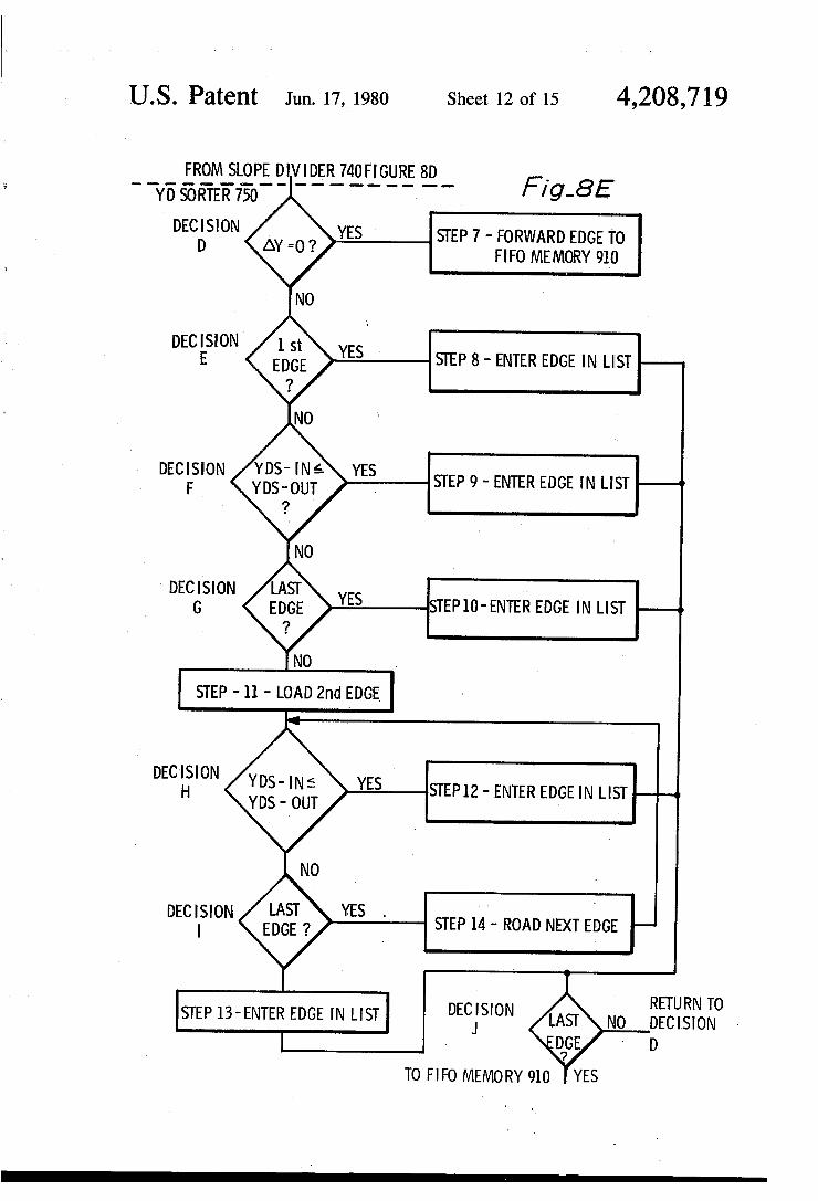
General mains ambiguity as to whether the face is within view. Referring to FIG. 26 showing image window 262, 4 l5 FIG. 7 shows edge stage 65 having Xd processor rays (Rl, R2, R3, and R4) extend from the four corners 706X and Yd processor 706Y which receive projected (Cl, C2, C3, and C4) of window 260. If a ray is inter- face vertex coordinates (Xd and Yd) from projection sected an odd number of times by the edges of the poly- stage 64 and Provides face edge lists to display genera- gon face, then the corresponding comer is surrounded 2o tor 44. Each edge is defined by edge data including a by the polygon. This technique can be implemented by starting Point (Xd% YdS), the y coordinate of the termi- inspecting the out-codes of the adjacent vertices &fin- nation Point (Y% PIUS the slope of the edge (delta ing each edge. The criterion for crossing the rays is Wdelta Y). very similar to the rejection criterion and is by The Y coordinates of each set of face vertices (Xd
t(l)=sign t(2)= 1 and sign 1(1)#sign l(2). advanced to previous Y register 716 in CCW order as defined in data base 48. Each current Y coordinate
PROJECTION STAGE 64 (Ydc) and previous Y coordinate (Ydp) are forwarded to adder 720 for calculating a delta Y for each face edge General or pair of points (delta Y=Ydc-Ydp). Simultaneously,
FIG. 6 ~hows Projection and clipping stage 64 of 30 each Ydc and Ydp are entered into Y start multiplexer image processor 42 which projects three-dimensional 730s and y terminate multiplexer 730t. The starting y window coordinates vl, vt, and Vz from clipping stage coordinate Yds is the end point of each face edge that is 63 into a two-dimensional vector Vd (Xd, Yd). The scanned first on CRT 82; and the terminate Y coordi- projected vectors Vd define the end points of each face nate Ydt is scanned last. In the embodiment shown, the edge for face generation stage 65. The projection is 35 conventional top to bottom scan is employed. There- accomplished by dividing vl and vt by Zc through a fore, the start point Yds is always the smaller of the two binary division nonrestoring technique (described in adjacent points Ydc and Ydp. The sign bit of delta Y “Digital Arithmetic-I” by Y. Chu pages 39-43). Z/2 (SIGN BY) defines which is smaller, Ydc or Ydp, as registers 610-1 and 6104 load the divisor Zc/2, and 4o follows: MUX/Register 620-1 and 620-t select and load the divi- dend v1/2 and vt/2 in response to control logic 70. The
MUX/Registers 620 may be 24 bit 2:l multiplexers
ALU’s 630 may be 16 bit flowthrough arithmetic
Sign gates 636 may be exclusive OR gates (74386). Quotient registers 640 may be 12 bit shift registers
(three 74164’s) for receiving the Projected data x d and
may be a 24 bit shift register (six
logic units (four 74S181’s+one 743182). 5
face edges and pyramid of vision 250 define the new Yd one bit at a time as it is generated by ALU’s 630. zc register
CIF register 660 may be a series of 74S174‘s.
logical operations. As an example, R1 is crossed if sign 25 and yd) are loaded into current y mux-register 710 and
for - delta Y ydc = yds, and Xdc = Xds Xdp = Xdt, and Xdp = Xdt
for + de,ta inputs to registers 610 and 620 are right-shifted by One digit to establish the division by two. Arithmetic logic
ydc = ydt, and Xdc = Xdt Ydp = Yds, and Xdp = Xds
unit ALU 630-1 and 630-t then receive the dividends 45 through shift return loops 623-1 and 6234, or subtract Zc/2 thereto in response to a -+function from logic 70. The dividend +Zc/2 term is loaded into MUX’620, returned to ALU’s 630, and then combined with an- other &Z/2. The output of ALU’s is slew wired with 50 respect to the input of MUX’s 620 causing a division by two right shift. The vl/Vz and vt/Vz quotients are generated one bit at a time, MSB first, by comparing the sign bit (MSB) of Zc with the sign bit of the partial remainders with MUS 620 through sign gates 636-1 and 55 636-t. The quotient bits individually enter quotient reg- isters 640-1 and 6404, and are left-shifted by control Xd processor 706X has the Same hardware as Yd logic 70- ZC on line 592 from range register 590 is loaded into renormalization register 650 and right- Current y mux-register 710 may be a 12 bit 2:1 multi- shited by control logic 708 the same number of places as 60 plexer-register (three 74298’s) for the current vertex of were Ieft-shifted in normalizer 370 in translation stage each face as the vertices are received in C c w order 60. Color, intensity, and flag data on line 592 from CIF from quotient registers 640-1 and 640-t. register 590 is loaded into CIF register 660 in response Previous Y register 716 may be a 12 bit storage regis- to control logic 70. ter (two 74174‘s) for holding the vertex just preceding
First vertex Y register 718 may be a 12 bit storage DETAILED DESCRIPTION register (two 74174’s) for holding the first vertex while the intermediate vertices are processed. The first vertex
processor 706Y, and is therefore not shown in detail.
65 the current vertex.
Z/2 register 610 may be a 24 bit register (four 74S174‘s).
and activates multiplexers 730s and 730t accordingly. Slope divider 740 provides the slope of each edge face by computing delta X/delta Y ffor the corresponding pair of vertices.
The face edges are arranged in scan order by Yds sorter 750 according to the smallest Yds. Each edge data set is loaded into sorter 750 in CCW order and forwarded to image generator 44 in order of smallest Yds for accomodating the top to bottom scan.
DETAILED DESCRIPTION

4,208,7 19 19 20
is loaded into current mux-register 710 as the last vertex (b) a 16 word 5 bit pointer RAM (two 743189’s) for is advanced to previous vertex status to form the last storing the RAM pointers. edge of the face. (c) a three level pointer pushdown stock (two mux-
Adder 720 may be a 12 bit adder (three 74283’s) for registers 74298’s-fust level, one 74S174-second calculating delts Y=Ydc-Ydp, and forwarding SIGN 5 level, and one 74S174-third level) for manipulat- Y to Y and X multiplexers-registers 730s and 73Ot. ing pointers into sorted order each time a new key
Inverter 722 may be a 12 bit inverting buffer (two is received by the key data RAM. 74S04’s) for inverting Ydp into -Ydp. The carry in on (d) address counter (one 74161) and smallest key adder 720 is forced to 1 to complete the complement of pointer register (one 748174) for generating RAM Ydp. 10 addresses and storing the current smallest key
Start point and terminate point multiplexer-register RAM address. 730 may be 12 bit 2:l multiplexer-registers (three (e) RAM address multiplexer (two 74S153’s) and a 74298’s each) for simultaneously holding both Ydc and pointer RAM input multiplexer (three 74S153’s) Ydp available for selection as either Yds or Ydt. which cooperates with the three level stack and
address counter for selecting RAM addresses and (three 74S175’s) for holding delta Yc while divider 740 the pointer RAM input. forms the slope (delta Xp/delta Yp) for the previous (f,) an existing key register (three 74S175’s) and com- edge. Additionally register 724 may include a zero de- parator (three 74S85’s) for determining where to tect circuit (one 74330) for providing delta Y=O to insert the input key among the existing key in the control 70 when the slope is horizontal and the edge 20 key data RAM. The existing key register also may be omitted from further processing. stores key data to be advanced to image generator
44. division nonrestoring divider as described in projection (g) non key data output register (twenty-four stage 64, for calculating slope=delta X/delta Y. The 74S175’s) for storing non key data (Xds, slope, Ydt, dividend delta X may be right shifted into additional 25 Zc, and CIF) to be advanced to image generator
44. slope to accomodate a Y increment of one raster line. In the embodiment shown the right shift is nine places to accomodate a 1024 scan line, interlaced display (2 to the 9th=512).
Sorter 750 may be a 12 bit key-96 bit non key sorter for output edge data in order ascending of Yds, formed by:
(a) a 16 word 12 bit key data RAM (three 74S189’s)
Delta Y register 724 may be a 12 bit storage register 15
Divider 740 may be a 12 input bit-20 output bit binary
shift register (one 74166) for scaling down the resulting
CONTROL LOGIC Processor control logic 70 responds to instruction
30 code and data flags contained in the data flow from data base 48 for processing the coordinate data through image processor 42. The flow tables described below disclose the logic involved in controlling each stage of image processor 42. Various hardware circuit configu-
for receiving and storing the key data (Yds) in 35 rations could incorporate this logic. input order.
TRANSLATION STAGE 60-CONTROL LOGIC FLOW TABLE I. TRANSFER INSTRUCTION WORD CONTROLLER 46 TO REGISTER 310 STEP I A (1) Maintain LOAD signal on instruction
register 3 10. (2) Load next instruction from buffer register 306 into instruction regis- ter 310 (LOAD). Is image data available to translation stage 60 on data bus 3071 YES-STEP IB NO-STEP IA (1) Clear accumulator 370 (CLR). (2) Clear scaler data “S” from scale regis- ter in scaler 360. (3) Clear address counter 320A (CLR). (4) Set DAR from control logic 70, wait for DAV From interface controller 46. Decode four MSB of instruction in register 310A to identify one of sixteen instructions
DECISION IA: (DAW
STEP IB:
DECISION IB:
(0- 15). 11. LOAD X INSTRUCTION-LDX (0) STEP I I A (1) Load address counter 320A with four bits
of address “A” (LOAD). (2) Unit decrement word counter 320B (DEC).
DECISION IIA: DAV?
DECISION IIB: What is R? YES-DECISION IIB NO-DECISION IIA
R = l R = 2 R = 3 (fine 16 bit) (coarse 16 bit) (normal 24 bit) I. Load 16 1. Same as DE- 1. Load 16 LSB
LSB from bus CISION IIB from bus 307 307 into RAM (R = 1) 1 through into RAM 350X.
350X. 3 except load 2. Request DAR, 2. Load zeros 16 MSB at 1. wait for DAV.

21 -continued
4,208,719 22
TRANSLATION STAGE 60-CONTROL LOGIC FLOW TABLE
into RAMS 350 3. Load 8 MSB Y and 2. from bus 307
3.a. Unit in- into RAM 3WX. crement ad- 4. Load zeros
dress counter into RAMS 350 320A (INC). Y and Z. 3.b. Unit de- 5. Same as DE-
crement word CISION IIB counter 320B (R = I) 3.
(DEC). 3.c. Set DAR, wait for DAV. 4. DECISION 2. DECISION 6. DECISION
IIC. IIC. IIC. Is word count in register 320 B = O? YES-STEP IA NO-DECISION IIA
Same as STEP IIA.
DECISION IIC
111. LOAD Y INSTRUCTION-LDY (1) STEP IIIA: DECISION IIIA: DAV?
YES-DECISION IIIB NO-DECISION IIIA DECISION IIIB What is R?
from bus 307 into RAM 350Y.
2. Load zeros into RAMs 350
X and Z. 3. Same as DE-
CISION IIB (R = 1) 3.
R = 1 R = 2 R = 3 1. Same as DE- CISION IIIB from bus 307
1. Load 16 LSB 1. Load 16 LSB
(R = 1) 1 through 3 except load 16 MSB at 1.
into RAM 3WY. 2. Set DAR,
wait for DAV. 3. Load 8 MSB from bus 307
into RAM 350X. 4. Load zeros
into RAMs 350 X and 2.
5. Same as DE- CISION IIB
4. DECISION 2. DECISION 6. DECISION IIIC. IIIC. IIIC.
DECISION IIIC
IV. LOAD Z INSTRUCTION-LDZ (2) STEP IVA: DECISION IVA: DAV?
DECISION IVB What is R?
Is word count in register 320 B = O? YES-STEP IA NO-DECISION IIIA
Same as STEP IIA.
YES-DECISION IIB NO-DECISION IVA
R = l R = 2 R = 3 1. Load 16 LSB 1. Same as DE- 1. h a d 16 LSB
from bus 307 CISION IVB from bus 307 into RAM 3502. (R=l) 1 into RAM 3502.
2. Load zeros through 3, ex- 2. Set DAR, into RAMs 350 cept load 16 wait for DAV.
X and Y. MSB at 1. 3. Load 8 MSB 3. Same as DE- from bus 307
CISION I1 into RAM 3502. (R=l) 3. I 4. Load zeros
into RAMs 350 X and Y.
5. Same as D E CISION IIB (R = 1) 3.
4. DECISION 2. DECISION 6. DECISION IVC. IVC. IVC.
DECISION IVC
V. LOAD XY INSTRUCTION-LXY (3) STEP VA: DECISION VA: DAV?
Is word count in register 320 B = O? YES-STEP IA NO-DECISION IVA
Same as STEP IIA.
YES-DECISION VB NO-DECISION VA DECISION VB: What is R?
R = l R = 2 R = 3 I . Same as DE-
from bus 307 CISION VB from bus 307 1. Load 16 LSB 1. Load 16 LSB

23 4,208,719
-continued TRANSLATION STAGE 60-CONTROL LOGIC FLOW TABLE
into RAM 350X. (R = 1) 1 into RAM 350X. 2. Set DAR, through 5 , ex- 2. Set DAR,
wait for DAV. cept load 16 wait for DAV. 3. Load 16 LSB MSB at 1 and 3. Load 8 MSB
from bus 307 3. from bus 307 into RAM 350Y. into RAM 350X.
4. Load zeros 4. Set DAR, into RAM 3502. wait for DAV. 5. Same as DE- 5. Load 16 LSB
CISION IIB from bus 307 (R = 1) 3. into RAM 350Y.
6. Set DAR, wait for DAV. 7. Load 8 MSB from bus 307
into RAM 350Y. 8. Load zeros
into RAM 3502. 9. Same as DE-
CISION IIB
6. DECISION 2. DECISION 10. DECISION vc. vc. vc.
DECISION V C Is word count in register 320 B = 01 YES-STEP IA NO-DECISION VA
Same as STEP IIA.
YES-DECISION VIB NO-DECISION VIA
VI. LOAD A INSTRUCTION-LDA (4) STEP V I A DECISION V I A DAV?
DECISION VIB: What is R? R = l R = 2 R = 3
1. Load 16 LSB 1. Same as DE- 1. Load 16 LSB from bus 307 CISION VIB from bus 307
into RAM 350X. (R = 1) 1 into RAM 350X. 2. Set DAR, through 6, ex- 2. Set DAR,
wait for DAV. cept load 16 wait for DAV. 3. Load 16 LSB MSB at 1, 3, 3. Load 8 MSB
from bus 307 and 5. from bus 307 into RAM 350Y. into RAM 350X.
4. Set DAR, 4. Set DAR, wait for DAV. wait for DAV. 5. Load 16 LSB 5. Load 16 LSB
from bus 307 from bus 307 into RAM 3502. into RAM 350Y. 6. Same as DE- 6. Set DAR,
CISION IIB wait for DAV. (R = 1) 3. 7. Load 8 MSB
from bus 307 into RAM 350Y.
8. Set DAR, wait for DAV. 9. Load 16 LSB
from bus 307 into RAM 3502.
10. Set DAR, wait for DAV. 11. Load 8 MSB
from bus 307 into RAM 3502. 12. Same as DE-
CISION IIB
7. DECISION 2. DECISION 13. DECISION VIC. VIC. VIC.
DECISION VIC
VII. RECALL X-RCX (5) STEP VIIA: DECISION VIIA: DAV?
DECISION VIIB: What is R?
Is word count in register 320 B = O? YES-STEP IA NO-VIA
Clear address counter 320A (CLR).
YES-DECISION VIIB NO-DECISION VIIA
R = 2 (16 bit) R = 3 (24 bit)
24

25 4,208J 19
-continued TRANSLATION STAGE &CONTROL LOGIC FLOW TABLE
1. Load 16 MSB from bus 307 into RAM
350X. 2. Set DAR, wait for
DAV.
1. Load 16 LSB from bus 307 into RAM 350X.
2. Set DAR, wait for DAV.
3. Load 8 MSB from bus 307 into RAM 350X. 4. Set DAR, wait for
26
3. STEP XIIA. 5. STEP XIIA. VIII. RECALL Y-RCY (6) STEP VIIIA DECISION VIIIA. DAV?
DECISION VIIIB: What is R?
Clear address counter 320A (CLR).
YES-DECISION VIIIB NO-DECISION VIIIA
R = 2 (16 bit) 1. Load 16 MSB from
bus 307 into RAM 350Y. 2. Set DAR, wait for
R = 3 (24 bit) 1. Load 16 LSB from
bus 307 into RAM 350Y. 2. Set DAR, wait for
3. Load 8 MSB from bus 307 into RAM 350Y. 4. Set DAR, wait for
DAV. 5. STEP XIIA.
DAV. DAV.
3. STEP XIIA. IX. RECALL Z-RCZ (7) STEP IXA DECISION IXA DAV?
DECISION IXB: What is R?
Clear address counter 320A (CLR).
YES-DECISION IXB NO-DECISION IXA
R = 2 (16 bit) 1. Load 16 MSB from
bus 307 into RAM 3502. 2. Set DAR, wait for
R = 3 (24 bit) 1. Load 16 LSB from
bus 307 into RAM 3502. 2. Set DAR, wait for
3. Load 8 MSB from bus 307 into RAM 3502. 4. Set DAR, wait for
DAV. DAV.
3. STEP XIIA.
Clear address counter 320A (CLR).
5. STEP XIIA. X. RECALL XY-RXY (8) STEP X A DECISION X A DAV?
DECISION X B What is R? YES-DECISION XB NO-DECISION XA
R = 2 (16 bit)
1. Load 16 MSB from bus 307 into RAM 350X
2. Set DAR, wait for
3. Load 16 MSB from bus 307 into RAM 350Y
4. Set DAR, wait for
R = 3 (24 bit)
1. Load 16 LSB from bus 307 into RAM 350X. 2. Set DAR, wait for
3. Load 8 MSB from bus 307 into RAM 350X. 4. Set DAR, wait for
5. Load 16 LSB from bus 307 into RAM 350Y. 6. Set DAR, wait for
DAV. 7. Load 8 MSB from bus
307 into RAM 350Y. 8. Set DAR, wait for
DAV.
DAV. DAV.
DAV. DAV.
5. STEP XIIA.
Clear address counter 320A (CLR).
YES-DECISION XIB NO-DECISION XIA
9. STEP XIIA. XI. RECALL A-RCA (9) STEP XIA: DECISION XIA DAV?
DECISION XIB: What IS R?

27 4,208,7 19
-continued TRANSLATION STAGE 60-CONTROL LOGIC FLOW TABLE
R = 2 (16 bit) 1. Load 16 MSB from
bus 307 into RAM 350X.
2. Set. DAR, wait for DAV.
3. Load 16 MSB from bus 307 into RAM
4. Set DAR, wait for
5. Load 16 MsB from
3502. 6. Set DAR, wait for
DAV.
R = 3 (24 bit) 1. Load 16 LSB from bus
307 into RAM 350X. 2. Set DAR, wait for
DAV. 3. Load 8 MSB from bus
307 into RAM 350X. 4. Set DAR, wait for
350Y. DAV. 5. Load 16 LSB from bus
DAV. 307 into RAM 350Y. 6. Set DAR, wait for
7. Load 8 MBS from bus 307 into RAM 350Y. 8. Set DAR, wait for
DAV. 9. Load 16 LSB from bus
307 into RAM 3502. 10. Set DAR, wait for
DAV. 11. Load 8 MSB from bus
307 into RAM 3502. 12. Set DAR, wait for
bus 307 into RAM DAV.
28
7. STEP XIIA. XII. RECALL LOAD-RCL (10) STEP XIIA: (1) Load accumulator 370 (X, Y, and 2) with
“Vo” from RAM 350 (X, Y, and Z) at ad-
13. STEP XIIA.
DECISION XIIA.
STEP XIIB:
DECISION XIIB:
STEP XIIC
STEP XIID:
dress A = 0. (2) Unit increment address counter 320A (INC). (3) Load accumulator 370 (X, Y, and 2) with “-Vp” from RAM 350 (X, Y, and 2) at ad- dress A = 1 to form Vt = Vo-Vp. (4) Unit decrement word counter 320B (DEC). Is the face part of a three dimensional object (is 3D flag set)? YES-STEP XIIB NO-STEP XIIE (Three dimensional (Two dimensional case) case) (1) Wait for DAV. (2) Load Three D register 341 (LOAD). (3) Set DAR, wait for DAV. (4) DECISION XIIB. Is word count t 41 Vertex pointers are packed four to one sixteen bit word. YES-STEP XIIC NO-STEP XIID (1) Wait for DAV. (2) Load Three D register 342. (3) Set DAR, wait for DAV. (4) STEP XIID. (1) Load address counter 320A with first ver- tex pointer “A” from register 310A. (2) Load scaler 360 with “S” from register 310B. (3) Load accumulator 370 with the A V data from RAM 350 as accessed by the pointer from the Three D buffers. (4) Clear address counter 320A. (5) Wait for DAR-T from Normalizer 380. (6) Enable FIRST VERTEX flag in CIF register. (7) Load the buffer register in accumulator 370 with the contents of the accumulator
(8) Clear “S” register in scaler 360. (9) Clear accumulator 370. (10) Unit decrement word counter 320B. (1 1) Load H and N address register 386 with “A” (LOAD). (12) Load accumulator 370 with Vo. (13) Unit increment address counter 320A. (14) Load accumulator 370. (15) Load address counter 320A with vertex address from Three D register 341 or 342. (16) Load scale register within scaler 360.
(LOAD-B).

4,208,719 29 30
-continued TRANSLATION STAGE 60-CONTROL LOGIC FLOW TABLE
DECISION XIID:
STEP XIIE:
DECISION XIIC.
STEP XIIF
DECISION XIIE
STEP XIIG:
DECISION XIIF:
(17) Load accumulator 370. (18) Clear address counter 320A. (19) Wait for DAR-T. (20) Repeat items 7, 8,9, and 10 of STEP XIID (21) Same as STEP XIID items 12-19. (22) Same as STEP XIID items 7-10. (23) Load last vertex flag into CIF registers when B = 0. (24) DECISION XIID. Is word count B = 07 YES-STEP IA NO-DECISION XIIE
(1) Same as STEP XIID items 1 and 2. (2) Wait for DAR-T. (3) Same as STEP XIID item 7. (4) Set first vertex flag. (5) Load accumulator 370. (6) Increment address counter 320A. (7) Decrement word counter 320B. (8) DECISION XIIC. Is word count B = O? YES-STEP IA NO-STEP XIIF (1) Wait for DAR-T. (2) Same as STEP XIIE items 4-7 except set last vertex flag when B = 0. (3) DECISION XIIC. Is product of Visibility Test positive or negative? POSITIVE-STEP IA NEGATIVE-STEP
(Visibility Test)
XIIG (1) Same as STEP XIID items 20-23. (2) DECISION XIIF Is word count B = O? YES-STEP IA NO-STEP XIIG
XII. COLOR INTENSITY FLAG-CIF (1 1)
CIF data from bus 307. Word counter 320B is decremented after each load until B = 0. XIV. STRING INSTRUCTION-STG (12)
In this instruction the initial face of a stridg of faces is processed from RAM 350 through translation stage 60 into rotation stage 62 as a string of light points or four sided faces. The vertices of the four sided faces are re- trieved from RAM 350 in CCW order as described in “XI. RE- CALL A-RCA(9):’
In this instruction the CIF registers are loaded with
XV. LOAD H-LDH (13) AND LOAD N-LDN (14) In this instruction data is loaded into H/N address
register 3 from data bus 307, and then into H/N RAM 410 as described in Section VI. H M Ram 410 receives the data during an idle oortion of its cvcle.
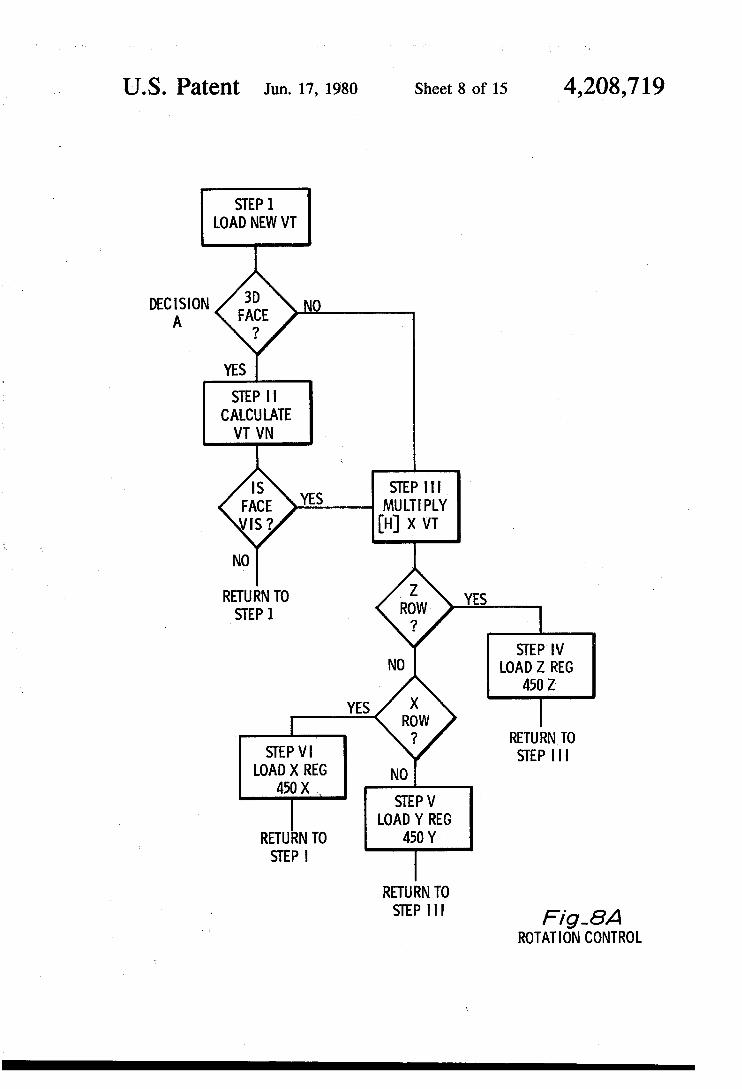
CLIPPING STAGE 63 FIGS. 8 B and C show the logic diagram for the
ROTATION STAGE 62 control of clipping stage 63. The first point coordinates FIG. 8A shows the logic-diagram for the processing are loaded into multiplexers 520 (Step 2) and the out-
of translated point coordinates (Vt) from translation code (OC) for each point is determined by window stage 62. Each new Vt is loaded into multiplexers 416X, circuits 510. The object code in CIF register 590 is Y, and Z (Step I). The object code in CIF register 460 55 examined to determine whether the first coordinate is which accompanies each new Vt is examined to deter- really a polygon vertex (or line end point) or merely a mine if the new Vt is associated with a 3D face requir- single light point (Decision A). In the case of vertices ing visibility testing (Decision A). If so, the dot product (and end points), the next vertex (or other end point) is of Vt.Vn (from N RAMs 410X, Y, and Z) is calculated loaded and outcode (OC) determined (Step 4). The (Step 11). The sign bit of the dot product reveals 60 Oc‘s are examined to determine if the edge defined by whether the 3D face is visible or not (Decision B). The the two vertices crosses the Z=O plane (Decision C). If vertex of visible 3D faces (Decision B-yes) and the the edge crosses the Z=O plane, then the intersection remaining non3D face vertices (Decision A-no) are point is determined by a binary search (Step 5). If the multiplied by the three x three H matrix in H RAMs edges do not cross the Z=O plane, then the Oc‘s of 410X, Y, and Z to provide the rotated vector Vc - Zc 65 both points are examined to determine if they both are first, Yc second, and Xc last (Step 111). Each coordinate in front of pilot’s eye 220 (Z=O plane) or behind pilot’s is loaded into registers 450X, Y, and Z as they are calcu- eye 220 and therefore definitely not visible (Decision lated (Decision C and D, Steps IV, V, and VI). D). The endpoints of edges which intersect the Z = O
50

50
55
60
65
4,208,7 19 31 32
DISPLAY GENERATOR 44 plane or which are completely in front thereof, are examined via their OC for visibility (Decisions F, G, and H, and Step 8). If both endpoints are out of view Texture Stage 72
(Case 3) the OC'S are examined to determine if Clipping Texture Stage 72, shown in FIG, 9, provides mini- is required (Decision I). If both endpoints are in view raster data for the set of horizontal Scan lines forming (Case 1) or otherwise do not require clipping, the next each face. The miniscan lines progressively increase vertex coordinates are loaded. If only one vertex is in and/or decrease in response to the face edge list (Xds, view (Case 2) or clipping is otherwise required (Case 31, Yds, Xslope, and Ydt for each edge) from face genera- the edge is processed through the appropriate series of tion stage 65. The miniraster data for each miniscan line binary search routines based on the Oc's (Decision J). lo includes the Xd coordinate of the left hand end point The binary search routines determine the interception (XdL), the width of the miniscan line 0, the Yd coor- points of the edge with the left, right, bottom or top dinate (Yd scan), Zc and CIF. boundaries of image plane 262. Each interception point The edge list is loaded into memory 910 in ascending becomes a new vertex of a new polygon formed by the 15 Yd order by face order Once each frame, and extracted visible portion of the original polygon face. in the same order twice each frame-once for the field
of even miniscan lines, and once for the field of odd miniscan lines. X coordinate generators 920L and 92OR provide XdLc and XdRc respectively for each miniscan
projection stage a4, processor 706X and y, and slope 20 line by combining Xds with the Xslopes of the two
are loaded into registers 610 for projection division of the scan line. XdLs is incremented by the left hand (Step 1). The quotients (projected points) are forwarded 'lope (xL 'lope) to form each XdL* and XdRs is
mented by the right hand slope (XR slope) to form each from registers 640 to edge stage 65, where it is examined XdR. Only generator 920 is shown in detail. Slope mul- for face data (Decision A). Non face data such as points 25 tiplexer 928 divides the xL slope by two (select
EDGE STAGE 65 FIG, 8~ shows the logic diagram for the control of
divider 740. The clipped points from clipping stage 63 Opposed edges Of the face which contain the end points
and line segments are forwarded memory 910* Each face data Point is
to for a first
(Decision B), which are loaded in v1 register 718 and Current Yd multiplier register 710 (Step 2). Each
START) for the first scan line of the even field, to accomodate the one half scan height displacement be- tween the interlaced odd and even fields on display 82. During the remainder ofthe display cycle, the XL slope
non fist vertex is loaded into register 710 as the current 30 is passed through slope multiplexer 928 without division Yd and the Previous Yd is advanced to register 716 (select ACC) to accomodate the proper height spacing (Step 3). Xd is similarly Processed through Processor between adjacent miniscan lines in the same field. 706X. Delta x and delta Y are calculated from their Adder 930 combines the x coordinate of the previous current and previous values, and loaded into registers 35 scan line (XdLp) with the current XL slope to provide 724 (Step 4). When the last vertex becomes the previous the current X coordinate (XdLc). Output multiplexer vertex in register 716 (Decision C), the face is closed by register 940 provides either XdLs (select START) or advancing V1 from register 718 to register 710 as the XdLc (select ACC) to miniraster data register 950. current vertex (Step 5). The last slope is calculated from Subtractor 952 provides the width W of each scan line the previous vertex (Vlast) and the current vertex (Vl) 40 by subtracting XdLc from XdRc (output of generator and entered into register 724. The slopes are calculated 92OR). The Y coordinate of the miniscan lines (Yd scan) by slope divider 740 as the delta p s and delta y's are is similarly formed by incrementing Yds with Yslope provided (Step 6). from Yslope generator 960. At the end of each edge, Yd
scan equals or exceeds the Ydt on the left edge (YdLt) TEXTURE STAGE 72 45 or right edge (YdRt). The signals Yd scan BYdLt and
Yd Scan BYdRt indicate to Control logic 70 that the next xL is required in Xd generators 920.
FIG. 8E shows the logic diagram for the control of Yds sorter 750. Input face edges are loaded into sorter 750 and examined for horiZonta1 edges-delta Y=O (Decision D). Horizontal edges are forwarded to FIFO memory 910 (Step 7). The non horizontal edges are examined for a first edge (Decision E). The first edge is entered at the start of the sort list (Step 8). Non first edges are examined to determine whether the input Yds is less than the last or output Yds in sorter 750 (Decision F). Smaller input Yds are entered at the start of the sort list (Step 9). Larger Yds are examined for a last edge (Decision G). Last edge is entered in last place of sort list (Step 10). The second edge is loaded (Step 11) and examined for input Yds less than the last Yds in sorter 750 (Decision H). Smaller Yds are inserted in the sort list (Step 12). Larger Yds are examined for last edge (Decision I). Last edges are entered into the sort list (Step 13). If the input edge is not the last edge, the next edge is loaded (Step 14). The input edge is again exam- ined for a last edge (Decision J)-return to Decision D of flow chart for non last edge, and output sorter 750 to FIFO memory 910 for last edge.
Or XR
DETAILED DESCRIPTION FIFO memory 210 may be a 2048 wordsx 100 bits
memory (two hundred 82Sll's) for sequentially output- ting the complete edge list twice each cycle. Memory 210 interfaces with the remainder of miniraster calcula- tor 72 through a 100 bit register (twenty five 74S175's).
XL slope register 924 may be a 20 bit storage register (five 74S175's) for holding each new Xslope as they are provided by memory 910.
XL slope multiplexer 928 may be a 20 bit 2:l multi- plexer (five 74S157's) with the START input right shifted to provide a division by two. The START and ACC select are provided by control logic 70.
XL Adder 930 may be a 20 bit adder (five 74283's) for incrementing each previous X left coordinate (XdLp) by the current XL slope.
Limit muliplexer 934 may be a 20 bit 4:l multiplexer (ten 74S153's) for preventing underflow and overflow when an edge approaches the display boundary. The

4,208,719 33 34
VIDEO CONTROL 76 four inputs are XdLc (twice), all ones (overflow), and all zeros (underflow). The two select inputs are the sign bits of XdLc and XL slope. Underflow occurs when Video control 76 receives color and intensity data both sign XdLc and sign XL slope are negative. Over- from CIF 660 in Projection stage 64 for each face being flow occurs when sign XdLc is negative and sign XL 5 displayed to control the color and display brightness of slope is positive. the scan lines forming that face. If desired, the display
XdLs register 938 may be a 12 bit register (three intensity may be attenuated by Zc data for range simula- 74S1759s) for holding the coordinate of the starting tion. Suitable video control techniques are also dis-
closed in detail in U.S. Pat. No. 3,999,308.
FULL RASTER EMBODIMENT end point of the current edge (Xds) as it is provided by FIFO memory 910. 10
Output multiplexer register 940 may be a 2o bit 2:1 If desired, the edge list from register 760 may be register (five 25s09’s) for accumulating displayed on a full raster in the conventional frame XdLc and Outputting either XdLs Or XdLc. The output manner across the entire Screen of display device $2. is returned to d d e r 930 and forwarded to miniraster 15 The vertices of all visible polygon faces (or visible per- data register 950. tions thereof) for each frame are sorted by Yds to ar-
Miniraster data register 950 may be a 76 bit register range the vertices in display order by raster. Next, the (nineteen 74s175’S) for holding the miniraster data contents of each scan line are sorted by Xds to arrange (XdLc 12 bits, W 12 bits, Yd scan 12 bits, CIF 24 bits, the vertices in display order by raster. Next, the con- and Z 16 bits. 20 tents of each scanline are sorted by Xds to arrange the
Subtractor 952 may be a 12 bit subtractor (three vertices in order of display within each scanline. The 74283’s and two 74S04’s) for providing the width of resulting Yds - Xds sorted edge list with accompanying each miniscan line (W=XdRc-XdLc) to register 950. slope and Yds data is processed through a conventional
Yslope generator 960 may be a 12 bit register (thee full raster display generator which provides the neces- 74S17vs) hardwired to specify the maximum number of 25 sary Vertical and horizontal sweep voltage waveforms.
EDGE SMOOTHING DEVICE 78 miniraster scan lines per frame. This number defines the scan density or Yslope.
Yslope multiplexer 964 may be a 12 bit multiplexer lo shows edge smoothem l 0 l o B 9 l0loG, and
30 of display device 82. The color data is passed through D/As 1014 and combined with the color data by means
(two 748157’s) similar in function to Xslope multiplexer 1OlOR for the three primary colors blue, green, and red 928.
Adder 968 may be a l2 bit adder (three 74283’s) for of weighting register network 1018. The resulting inten- sity-color signals are applied to the corresponding edge the l2 bits Of with the l2 bits Of
coordinate of the previous scan line (Ydp) to form the Y smoother 101OB, 101OG, and 101OR. Red edge 35 smoother lOlOR is shown in detail and includes high coordinate of the current scan line (Yd scan).
register (three 25SWs) similar in function to output back impedance 1024 between output junc- multiplexer register 940. tion 1026 and input junction 10281. Amplifier 1020 has a
Ydt register 974 may be a Pair of 12 bit registers (six plurality of feedback paths (FB:O through FB:N) each 74S17W for holding the Yd coordinates of the left 40 having one of a corresponding feedback capacitor (C:O hand edge termination point (YdLt) and the right hand through CN) and double-throw single-pull switching edge termination point (YdRt) which are periodically devices (SW:O through SW:N). Each feedback path, forwarded by FIFO memory 910. having one terminal (output terminal 1032) connected
Comparator 978 may be a pair of 12 bit comparators to amplifier output junction 1026 and having the other (six 74S85’s) for comparing Yd scan with YdLt and 45 terminal (switched terminal 1034) connected to the YdRt to determine the end of each edge. associated switching device. The switching devices
operate to connect switched capacitor terminal 1034 to either ground or to amplifier input 1028 depending on the content of input register 1040. Register 1040 has
a series of XdLc’s and wpS for generating the sweep 50 binary places BP:O through BP:N, one for controlling each switch sw:o through sw:N. The Size of the feed- back capacitors c:o through cN a power Of two
Multiplexer register 970 may be a 12 bit multiplexer gain, wide bandpass amplifier 1020 with negative feed-
DEFLECTION CONTROL 74 Deflection stage 74 receives Yd Scan accompanied by
voltages which provide the series of horizontal scan lines outlining each polygon face. Yd scan identifies vertical position of the first vertex. XdL identifies the series, each capacitor having twice the value of the
preceeding capacitor starting with C:O=C and ending mines the length of each scan line. Conventional inte- 1034 of selected capacitors to input junction 1028 and
propriate and ramp deflection The capacitors, the total feedback capacitance C:t may have ramp changes at a uniform rate to any one of 2Nseparate integer multiple values between move the CRT beam vertically across the face being GCC” and 662~2NC.99 The number contained in the N
ramps change at a much faster rate binary places of input register 1040 define which of the starting from an XdL to move the beam horizonW’ a 2N feedback capacitance values for C:t is in effect. distance indicated by the associated w. Suitable deflec- The value ofthe total feedback capacitance C:t has an tion techniques are disclosed in detail in U.S. Pat. NO. inverse proportionate affect on the bandpass of ampli- 3,999,308 entitled “Real-Time Simulation of a Point 65 fier 1020. Capacitance C:t lowers the upperpass limit System Having Textured Areas as Viewed by a Moving shunting high frequencies at output 1026 to input 1028 Observer” issued on Dec. 28, 1976 to Robert Louis where they are suppressed to a negligable value due to Peters. the high gain and negative feedback relationship. As a
left hand Of each scan line deter- 55 with C:N=2NC. By connecting the switched terminal grater techniques may be to provide the aP- grounding switched terminal 1034 of the remaining
at yd
The

4,208,719 35 36
consequence, the response time of amplifier 1020 is to grounding FET 1120 may precede the activating FB decreased causing color and intensity changes in the video data to occur gradually over a small scan dis- tance. Without edge smoothing, each variation in color
ENABLE voltage to feedback FET 11N (as shown in FIG. 12a and &). The switching sequence is biased towards a harmless momentary floating status on
and intensity along a scanline has a very high rate of 5 switched terminal 1034, in order to avoid the opposite change and occurs almost instantaneously on display 82 situation where input 1034 is momentarily forced to (see producing a discrete difference in the
at that point dong the scanline* A series Of these actual ground instead of the virtual ground quiescent point. The charge on capacitance C:t does not during the brief floating period because the switching of discrete differences are displayed across a group of
continuous scanlines to generate the edge of a face. The 10
scanlines caused by the slope of an edge produces the lation between the video output at junction 1026 and the undesirable ~ s ~ ~ ~ i ~ ~ ~ ~ ~ ~ effect. The selectable response switching transients generated within grounding FET time of edge smoother 78 each discrete differ- 1120 due to the small interelement capacitance therein. ence in intensity and color to have a selectable slower 15 Deactivation switching noise from grounding FET rate of change (see FIG. 124 which creates blending 1120 cannot Pass through the not Yet activated switch- Over a short time of the initial intensity level into the ing FET 1110 and cause undesirable transients in the subsequent intensity level. The ‘‘staircase’’ is dispersed video signal to CRT displays 82. Switching FET 1110 is across the slight scanning distance required for the activated after the deactivating switching transients blending of the discrete intensity differences. The edge 2o from grounding FET 1120 have expired. Similar activa- smoothing or blending period is directly determined by tion switching transients generated in switching FET the RC time constant total feedback capacitance C:t and 1110 are not isolated from VIDEO, but are neutralized feedback register 1024. by a corresponding inverted transient applied to input
FIG. 11 shows the “i-th” feedack path of an embodi- injunction 1028 through compensation capacitance ment of edge smoothing circuit 1010. Switching device 25 1140. Capacitor 1140 is charged simultaneously with SW:i is formed by two FETs, input FET 1110 and switching FET 1110 by an inverted FB ENABLE sig- grounding FET 1120s each having one elamnt con- nal from invertor 1144. The resulting compensation nected to switched terminal 1034 of capacitance C.i. A transient appears at input junction 1028 at the same tirne high voltage (FB Enable) from binary Place of as the activation switching transient from FET 1110.
feedback capacitor c:i to be one Of the selected capaci- of switching FET 1110 to a subvisible level. tors forming the total feedback capacitance C:t. A low voltage (GRD ENABLE) from BP:i deactivates DETAILED DISCLOSURE
FET ‘120 to remove the ground from switched terminal 1034 of C.i.
Preferably, amplifier 1020 is operated in the full pass- mode, and then reduced to lower pass frequencies.
grounded (non-selected) by residual zeroes in input
the output voltage at junction 1026. Input junction 1028 40 low capacitance, precision resistors for mixing the in- has a quiescent point at virtual ground due to the high tensity data and color data. The resistive value may gain characteristics of amplifier 1020 and negative feed- vary depending on the value Qf impedance 1024, the back resistance 1024. The input voltage at junction 1028 gain of amplifier 1020 and the desired weighting be- is continuously driven down by the feedback voltage tween intensity and color. For a 50/50 weighting at a generated by the feedback current through feedback 45 gain of two, with an 800 ohm resistor 1024, the pre- resistance 1024: ferred value of each of the six weighting resistors 1018
is about 400 ohms. Amplifier 1020 may be a high frequency, high slew
rate operational amplifier (M. S . Kennedy model 750) This normally virtual ground condition of input junc- 50 with the non-inverting input connected to the reference tion 1028 and the actual ground at switched terminal potential-ground.
switched into the associated feedback path without a of from about 5oo to about looo ohms, 800 being pre- significant change in the charge status of the capacitor. ferred for the model The switched terminal of the capacitor is switched from 55 A thermally stably low capacitance precision resistor an actual ground potential to a virtual ground quiescent point which minimizes the feedback capacitive transient is preferred.
A stabilizing capacitor of about 10 p.f. may be con- current incident upon switching. The fullpass mode (et =o) corresponds to the fastest nected across the resistor for minimizing overshoot and
risetime, having the greatest ratio of change. The rise- 60 undershoot* time is extended from the steepest rise to a slower rise in R-C network 1030 may be a 220 P.f. capacitor con- response to SLOPE data. As each new edge is encoun- nected aCrOSS an 82 ohm resistor, for minimizing unde- tered during each scan, a new set of feedback capacitors sirable operational amplifier transients which cause the is selected in response to the slope of that edge. If de- feedback waveform to deviate from the ideal R-C re- sired, the actual ground may be removed from switched 65 sponse curve. Such transients are especially objection- terminal 1034 just before connecting switched terminal able during the initial portion of the response curve. 1034 to the virtual ground of amplifier input injunction Input register 1040 may be an N bit line receiver 1028. That is, the deactivating GRD DISABLE voltage (10125’s) for independently activating the N switches.
offset between the discrete differences along adjacent deactivation Of grounding FET ‘120 provides
input register activates input FET l1l0 causing 30 Interference cancellation reduces the transient impact
Intensity D/A 1014 may be a high spud, low glitch, 35 digital to analog converter (DDC Model ADH 030-8)
for converting intensity and color digital data into an
preferred for high ‘peed Each feedback capacitor is therefore normally andog signal. Emitter coup1ed logic compatibility
register 1050, permitting the charge thereon to follow Weighting resistors 1018 may be thermally
Vinput=Vfb=IFbXR 1024
1034 Of each capacitor permits the capacitors to be Impedance 10% may be a resistor having a resistance
amplifier.

4,208,719 37 38
Rise time controller 1050 may be an N bit line driver each face, for providing edge smoothed digital display (10132's) for storing SLOPE data between clock peri- data to a raster type display device, comprising: ods and advancing SLOPE data to input register 1040 image processor means for receiving the image posi- in response to CLK from control logic 70. tion data and providing display coordinates for
Switches 1110 and 1120 may be high speed FETS 5 each vertex of each polygon face; (Signetics Quad Switch SOOOB). display generator responsive to the display coordi-
Capacitors C:l through C:N may be low leakage nates for determining the leading and trailing inter- mica capacitors. The values of a series of five capacitors sections of each face with each scanline of the suitable for a pixel dimension of about 25 nanoseconds display raster, and responsive to the image visual and a feedback resistance of 800 ohms are: data for providing a video signal to the display C:O= 30 pfs device along each scanline between the leading and C:1=60 fps (62 fps may be employed) trailing intersections of each face for generating the c 2 = 120 fps visual characteristics for that face on the display; c 3 = 240 fps and C:4=480 fps (470 fps may be employed) edge smoothing means for decreasing the rate of Inventor 1144 may be formed by one section of the change of the video signal in each scanline at the
line receiver of register 1040. intersection of that scanline and at least one edge of Variable capacitor 1140 may be an external capacitor each face, for causing a more gradual change of the
(0.5-2.0 fps) for adjusting the compensation wave visual characteristic prior to that intersection into shape. 20 the visual characteristic subsequent to that inter-
section by extending or contracting the intersec-
2. The image data system of claim 1, wherein the controlled rate Of change Of the video signal at the
able, capacitance feedback paths which may be selected 25 scanline intersection is a function of the slope of that to vary the response time of the analog circuit. The leading and trailing edges of intensity-color video data 1y wherein the
time, causing a graded change in intensity and color scanlines extending along a first direction and spaced along each face edge. The feedback pair of alternately 30 from one another along a second direction, and the rate activated switches in each path are responsive to slope Of change Of the video data for each edge for increasing the intensity-color scanline intersection, varies as the ratio of the spacing
scanlines divided by the distance along the first direc- - the horizontal. One switch of each pair is setially
loop as that feedback path is selected. The other switch
that path is not selected. Switching transients from the grounding switch are isolated from the video data by 40 activating the series switch last during selection and deactivating the series switch first during unselection. Transient charge current across the feedback capacitors is minimized by maintaining the switched side of the capacitor at ground Potential through the grounding 45
10
15
CONCLUSION tion transient period. The object of this invention has been accomplished
by providing an analog circuit with a series of switch-
face edge* 3. The image data system Of
along each Scan line are integrated or extended Over display raster is formed by a plurality of spaced parallel
across that face edge
transition time as the slope ofthat edge approaches zero distance the second dimension between adjacent
35 tion between adjacent intersections of that face edge. connected in each feedback path, and completes the 4. The image data system of claim 2, wherein the controlled rate of change of the video signal is directly
Of each pair grounds the feedback capacitance when propo~iona~ to the slope of that face edge, and
slope=delta I,delta 2;
where delta 1 is the spacing between adjacent scanlines and delta 2 is the changing position along the second direction of adjacent intersections along that face edge.
5. The image data system of claim 4, wherein the switch while unselected. During switching, the capaci- tor is disconnected from ground and connected to the vertical ground at the amplifier input through the series switch. The collective R-C time constant of the selected feedback paths varies at the slope of the current edge and is generally equal to the pixel time period.
It will be apparent to those skilled in the art, that various changes may be made in the apparatus and techniques described without departing from the scope of the invention. For example: The scan lines could be vertical, in which case the desired video risetime would be directly proportional to the slope of the edge. Fur- ther, substantial edge smoothing may be effected by blending only the intensity data and permitting the color data to maintain a step change. Accordingly, the scope of the invention should be determined only by the wording of the following claims and their legal equiva- lents.
We claim as our invention: 1. An image data system responsive to digital image
data including position data which defines the position of the vertices of polygon faces forming the image, and visual data which defines the visual characteristics of
scanlines are horizontal and delta 1 is a vertical incre- ment and delta 2 is a horizontal increment. 6. The image data system of claim 4, wherein the
image processor means provides the delta 1 increment 50 and the delta 2 increment between adjacent face edge -
scanline intersections along each face edge. 7. The image data system of claim 6, wherein the
image processor means further comprise a slope gener- ating means which provides the slope of each face edge
55 in response to delta 1 and delta 2 ffor controlling the rate of change of the video signal during the transient period associated with that edge - scanline intersection.
8. The image data system of claim 7, wherein the edge smoothing means includes an amplifier having an input
60 means and an output means with a plurality of selectable feedback paths between the inputt means and the output means responsive to at least onre face edge slope for controlling the rate of change of the video signal.
9. The image data system of claim 8, wherein each
a capacitor means having an output terminal con- nected to the amplifier output side of that feedback path, and having a switched terminal connected to
65 feedback path includes:

4,208,719 39 40
the amplifier input side of that feedback path when that feedback path is selected; and
least one face edge slope for independently select- 5 slope is a binary number, each bit of which increases the
responsive to the bit having the power of two corre- sponding to the power of two capacitance value of the the switched terminal of the capacitance means to
the amplifier input side of that feedback path when capacitor connected to that switch. 19. The image data system of claim 15, wherein the that feedback path is selected.
'9 wherein the reference voltage is approximately ground potential.
amplifier with the inverting input thereof forming the switching is a double throw-single pole switch- input means and the noninverting input thereof con- ing device. nected to a reference potential. 21. The image data system of claim 15, wherein the
11. The image data system of claim 10, wherein the switching means in each of the plurality of feedback amplifier means further includes a feedback impedance paths comprises: connected between the output means and the input a feedback switch for connecting the switched termi- means for maintaining a quiescent voltage at the input nal of the associated capacitance means to the am- means virtually at the reference potential.
12. The image data system of claim 11, wherein the a reference switch for connecting the switched termi- feedback impedance is a resistance. nal of the associated capacitance means to the ref-
13. The image data system of claim 11, wherein the erence potential.
where i is an integer giving the position of the capacitor means in the series of one through N, and where C is the capacitance value of the first capacitor in the series. a switching means connected to the switched
nal of the capacitor means and responsive to the at 18. The image data system of claim 179 wherein the
ing at least one of the feedback paths by switching value by a power of two, and each switching is
10 lo* The image data system Of
amplifier means is a high gain, high pass operational 20. The image data system of claim 15, wherein each
15
20 plifier input means; and
feedback impedance is a resistance and a capacitance 22* The image data system of claim 21, wherein the 25 switched terminals of currently unselected capacitors
which are about to be selected are disconnected from the reference potential by means of the reference switch prior to being connected to the amplifier input means by
of the feedback switch for isolating the input
connected in series. lo' wherein the
switching means in each of the plurality of feedback paths switches the switched terminal of the associated
capacitor means is selected and to the reference poten- tial when that capacitor means is not selected.
15. The image data system of claim 9, wherein the capacitance values of the capacitor means in the plural- compensation means for providing a compensation itY of fedback Paths forms a series of Progressively 35 signal to the input means simultaneously with and increasing values permitting the total selected feedback of the opposite polarity to each slope signal, which capacitance to have a number of possible values from causes the feedback switches to connect the the value of the smallest capacitor means to the value of switched terminal of the selected capacitors to the the sum of the capacitor means. input means.
24. The image data system of claim 23, wherein the number of selected feedback capacitance values C:fb is: compensation means includes an external capacitor for
each feedback switch having a capacitance substantially identical to the internal capacitance of that feedback switch .
25. The image data system of claim 21, wherein the switched terminals of currently selected capacitors which are about to be unselected are disconnected from the amplifier input means by means of the f ~ & a c k switch prior to being connected to the reference poten-
50 tial by means of the reference switch for isolating the input means from switching transients generated within
14* The image data system Of
capacitor to the amp1ifier input when that 30 means from switching transients generated within the reference switch.
edge smoothing 23. The image data system of claim 22, wherein the
further comprises;
16. The image data system of claim 15, wherein the 40 '
Number of C:fl=2N
where N is the number of feedback paths. 45 17. The image data system of claim 16, wherein the
capacitance value of each capacitor means in the series one through N is double the capacitance value of the preceeding capacitor in the series, so that the capacitance value (c) of each capacitor
C ( b 4 2 j C the reference switch.
is:
* * * * *
55
60
65